EP3300256A1 - Method for controlling digital-to-analogue converters and rf transmit circuit arrangement - Google Patents
Method for controlling digital-to-analogue converters and rf transmit circuit arrangement Download PDFInfo
- Publication number
- EP3300256A1 EP3300256A1 EP16190818.1A EP16190818A EP3300256A1 EP 3300256 A1 EP3300256 A1 EP 3300256A1 EP 16190818 A EP16190818 A EP 16190818A EP 3300256 A1 EP3300256 A1 EP 3300256A1
- Authority
- EP
- European Patent Office
- Prior art keywords
- dac
- digital
- analogue
- signals
- data signals
- Prior art date
- Legal status (The legal status is an assumption and is not a legal conclusion. Google has not performed a legal analysis and makes no representation as to the accuracy of the status listed.)
- Granted
Links
Images

Classifications
-
- H—ELECTRICITY
- H03—ELECTRONIC CIRCUITRY
- H03M—CODING; DECODING; CODE CONVERSION IN GENERAL
- H03M1/00—Analogue/digital conversion; Digital/analogue conversion
- H03M1/66—Digital/analogue converters
- H03M1/662—Multiplexed conversion systems
-
- H—ELECTRICITY
- H04—ELECTRIC COMMUNICATION TECHNIQUE
- H04B—TRANSMISSION
- H04B7/00—Radio transmission systems, i.e. using radiation field
- H04B7/02—Diversity systems; Multi-antenna system, i.e. transmission or reception using multiple antennas
- H04B7/04—Diversity systems; Multi-antenna system, i.e. transmission or reception using multiple antennas using two or more spaced independent antennas
- H04B7/06—Diversity systems; Multi-antenna system, i.e. transmission or reception using multiple antennas using two or more spaced independent antennas at the transmitting station
- H04B7/0613—Diversity systems; Multi-antenna system, i.e. transmission or reception using multiple antennas using two or more spaced independent antennas at the transmitting station using simultaneous transmission
- H04B7/0615—Diversity systems; Multi-antenna system, i.e. transmission or reception using multiple antennas using two or more spaced independent antennas at the transmitting station using simultaneous transmission of weighted versions of same signal
- H04B7/0617—Diversity systems; Multi-antenna system, i.e. transmission or reception using multiple antennas using two or more spaced independent antennas at the transmitting station using simultaneous transmission of weighted versions of same signal for beam forming
-
- G—PHYSICS
- G01—MEASURING; TESTING
- G01S—RADIO DIRECTION-FINDING; RADIO NAVIGATION; DETERMINING DISTANCE OR VELOCITY BY USE OF RADIO WAVES; LOCATING OR PRESENCE-DETECTING BY USE OF THE REFLECTION OR RERADIATION OF RADIO WAVES; ANALOGOUS ARRANGEMENTS USING OTHER WAVES
- G01S7/00—Details of systems according to groups G01S13/00, G01S15/00, G01S17/00
- G01S7/02—Details of systems according to groups G01S13/00, G01S15/00, G01S17/00 of systems according to group G01S13/00
- G01S7/42—Diversity systems specially adapted for radar
-
- G—PHYSICS
- G06—COMPUTING OR CALCULATING; COUNTING
- G06F—ELECTRIC DIGITAL DATA PROCESSING
- G06F1/00—Details not covered by groups G06F3/00 - G06F13/00 and G06F21/00
- G06F1/04—Generating or distributing clock signals or signals derived directly therefrom
- G06F1/10—Distribution of clock signals, e.g. skew
-
- H—ELECTRICITY
- H01—ELECTRIC ELEMENTS
- H01Q—ANTENNAS, i.e. RADIO AERIALS
- H01Q3/00—Arrangements for changing or varying the orientation or the shape of the directional pattern of the waves radiated from an antenna or antenna system
- H01Q3/26—Arrangements for changing or varying the orientation or the shape of the directional pattern of the waves radiated from an antenna or antenna system varying the relative phase or relative amplitude of energisation between two or more active radiating elements; varying the distribution of energy across a radiating aperture
- H01Q3/30—Arrangements for changing or varying the orientation or the shape of the directional pattern of the waves radiated from an antenna or antenna system varying the relative phase or relative amplitude of energisation between two or more active radiating elements; varying the distribution of energy across a radiating aperture varying the relative phase between the radiating elements of an array
- H01Q3/34—Arrangements for changing or varying the orientation or the shape of the directional pattern of the waves radiated from an antenna or antenna system varying the relative phase or relative amplitude of energisation between two or more active radiating elements; varying the distribution of energy across a radiating aperture varying the relative phase between the radiating elements of an array by electrical means
- H01Q3/36—Arrangements for changing or varying the orientation or the shape of the directional pattern of the waves radiated from an antenna or antenna system varying the relative phase or relative amplitude of energisation between two or more active radiating elements; varying the distribution of energy across a radiating aperture varying the relative phase between the radiating elements of an array by electrical means with variable phase-shifters
- H01Q3/38—Arrangements for changing or varying the orientation or the shape of the directional pattern of the waves radiated from an antenna or antenna system varying the relative phase or relative amplitude of energisation between two or more active radiating elements; varying the distribution of energy across a radiating aperture varying the relative phase between the radiating elements of an array by electrical means with variable phase-shifters the phase-shifters being digital
-
- H—ELECTRICITY
- H03—ELECTRONIC CIRCUITRY
- H03M—CODING; DECODING; CODE CONVERSION IN GENERAL
- H03M1/00—Analogue/digital conversion; Digital/analogue conversion
- H03M1/06—Continuously compensating for, or preventing, undesired influence of physical parameters
- H03M1/0617—Continuously compensating for, or preventing, undesired influence of physical parameters characterised by the use of methods or means not specific to a particular type of detrimental influence
- H03M1/0624—Continuously compensating for, or preventing, undesired influence of physical parameters characterised by the use of methods or means not specific to a particular type of detrimental influence by synchronisation
-
- H—ELECTRICITY
- H03—ELECTRONIC CIRCUITRY
- H03M—CODING; DECODING; CODE CONVERSION IN GENERAL
- H03M1/00—Analogue/digital conversion; Digital/analogue conversion
- H03M1/66—Digital/analogue converters
-
- H—ELECTRICITY
- H03—ELECTRONIC CIRCUITRY
- H03M—CODING; DECODING; CODE CONVERSION IN GENERAL
- H03M1/00—Analogue/digital conversion; Digital/analogue conversion
- H03M1/66—Digital/analogue converters
- H03M1/665—Digital/analogue converters with intermediate conversion to phase of sinusoidal or similar periodical signals
Definitions
- the invention relates to a method for controlling digital-to-analogue converters.
- the invention further relates to a RF transmit circuit arrangement.
- Transceiver devices for wireless communication systems typically comprise high speed analogue or digital front end (AFE, DFE) devices.
- AFE/ DFE devices typically comprise digital processors which are used to perform complex processing while adhering to reasonable power and size constraints.
- the data signals are normally first converted into analogue signals which may then be sent by a suitable antenna. The conversion process is performed by digital-to-analogue converters.
- DAC digital-to-analogue converter
- D/A digital-to-analogue converter
- D-A digital-to-analogue converter
- ADC an analogue-to-digital converter
- One technique to improve the sampling rate of a DAC system is to use multiple DACs in parallel.
- a parallel DAC architecture typically includes multiple DACs whose outputs are combined in the analogue domain.
- a single DAC element uses an externally generated clock signal.
- This clock signal is used within the DAC to generate a carrier signal which is then modulated with the transmit data.
- one problem with this approach is a potential misalignment of the different output signals of the DAC elements of a multi DAC array with regard to their phase shift.
- the clock generators which are triggering the DAC elements have to be reset regularly and sometimes for each data sample in order to ensure a predefined phase shift.
- this resetting is decreasing the data throughput significantly.
- a predefined phase shift is in particular essential for beamforming.
- Beamforming is used for transmitting RF signals in order to generate a predefined beam form.
- so-called smart multiple antennas are used.
- Smart antennas are arrays of antenna elements, wherein each of these antenna elements receive an analogue signal from a DAC. This analogue signals are to be transmitted with a predetermined phase offset and a relative gain.
- the net effect of the array is to direct a transmit beam in a predefined direction.
- the beam is steered by controlling the phase and gain relationships of the signals that excite the antenna elements of the array.
- US 8,286,067 B2 describes a method for transmitting sampled data and control information between a digital signal processor and an RF analogue front end device.
- the analogue front end device comprises two DACs within the transmit path.
- the clock signal for triggering these DACs is generated externally.
- the serial interface transmitter of the analogue front end device provides variable data rates by inserting null frames to match the data rate to the clock rate.
- the null frames may be identified by specific codes within the control field.
- US 8,286,067 B2 discloses a method for controlling multiple DACs within a modem, wherein the control data for controlling the DACs is included within the transmitted data.
- the problem addressed by the present invention is to provide a stable phase difference between the output signals of the DAC elements of a DAC array.
- this problem is solved by a method having the features of claim 1 and/or by a RF transmit circuit arrangement having the features of claim 8.
- the present invention is based on the finding that analogue RF output signals which are provided at the output of a DAC array compulsory need a stable phase shift to each other for specific applications, in particular for time division multiplex applications, for beamforming or the like.
- a first idea of the present invention is to shift the functionality of the clock generation inside every individual DAC element such that every DAC element is generating the carrier signal based on an internally generated clock signal.
- each clock generator within a DAC element is triggered independently by a separate control signal.
- This control signal comprises phase shift information for the corresponding and is generated by the digital interface circuit.
- the different DAC elements within the DAC array are each triggered by separate control signals such that the corresponding analogue RF output signals which are provided on the respective output terminals of each DAC element comprise a predefined phase shift to each other.
- the present invention is suitable for high performance and high speed applications.
- the analogue RF data signals which are generated by the multi-channel converter array and which are provided at respective output terminals of the DAC are each forwarded to antenna elements of an antenna array. This antenna array is then transmitting over the air RF signals based on the analogue RF data signals.
- the method is used for beamforming by setting a predefined shape of the beam.
- This predefined shape within the beam may be set via the control information of the control signal.
- Beamforming can be applied for radio or sound waves. Beamforming has various applications in radar, sonar, wireless communication, acoustics and biomedicine.
- a phased antenna array is used.
- a phased antenna array is an array of antennas in which the relative phases of the respective signals which are feeding the antennas are set in such a way that the effective radiation pattern of the array is reinforced in a desired direction and suppressed in undesired directions. It is very essential for those phased antenna arrays, that the phase relationships among the antennas may be fixed. In this case, however, it is essential to provide pre-defined phase shifts between the different analogue signals feeding the antenna elements.
- the present invention which provides such predefined phase shifts which enables a very smart beamforming technique.
- the digital interface circuit is a JESD204 interface, in particular a JESD204B interface. Consequently, the digital data signals which are fed into the DACs of the RF converter array and the control signals which are supplied to the DAC and their NCOs, respectively, are generated based on the JESD204 or specifically on the JESD204B transport protocol standard. As the resolution and speed of ADCs and DACs has increased in recent times, the demand for a more efficient interface has grown. The JESD204 interface brings this efficiency and offers several advantages over CMOS and LVDS interfaces in terms of speed, size and cost. JESD refers to a data interface that is able to support the high bandwidth necessary for high performance, high speed and multi-channel applications.
- JESD204 there is a significant reduction in input-output terminals which leads to smaller package sizes while reducing the number of digital input-outputs (IO) needed. Consequently, the JESD204 interface standard is easing board layout and circuitry. Very high speed ADCs and DACs, which are for example used for RF communication that would have previously required a complex interface design using a large number of FPGAs are now implemented within just a few IOs terminals. The total bandwidth of the JESD204 interface can also be separated into multi-channels based on the requirements of the application again without requiring additional IOs.
- the method further comprises the steps of coding an information of the starting phase, an increment and a point of time of switching into the control signal.
- the DAC is then analyzing this information. Based on the analyzed information, the clock generator of the DAC is switched. This switching may be conducted sample exact. This means, that each clock generator of a DAC is controlled sample exact with regard to the data samples of the digital data signals provided to the corresponding DAC.
- At least one control information per sample of the data signals is provided to each clock generator.
- each DAC is individually synchronized with regard to the frequency and phase of the carrier signal. Additionally, or alternatively, each DAC is individually and independently synchronized with regard to the analogue RF data signals. In particular, the controlling and/or synchronizing of the clock generators of each DAC is directly, individually and independently performed without resetting the clock generators.
- the digital serial interface circuit is a serial high-speed multi-channel time division multiplexing (TDM) interface.
- TDM time division multiplexing
- At least one of the clock generators is a numerically controlled oscillator (NCO).
- NCO numerically controlled oscillator
- a numerically controlled oscillator is a digital signal generator which creates a synchronous (i.e. clocked), discrete-time, discrete-valued representation of a specific waveform of the signal. Usually this specific waveform of the signal is sinusoidal.
- Numerically controlled oscillators offer several advantages over other types of oscillators in terms of agility, accuracy, stability and reliability. NCOs are very often used in communication systems, in particular for wireless communication, including digital up/down converters, digital PLLs, radar systems, drivers for optical or acoustic transmission, multilevel FSK/PSK modulators, demodulators and the like.
- the clock generator may also be a digitally controlled oscillator (DCO).
- DCO digitally controlled oscillator
- a DCO is a hybrid digital/analogue electronic oscillator which is very often used in frequency synthesizers.
- DCOs are a kind of a voltage controlled oscillator (VCO) and are designed to overcome the tuning stability limitations of early VCO designs.
- the RF transmit circuit arrangement further comprises an antenna array having a plurality of antenna elements. Each of these antenna elements is connected on their input terminals over data lines to a corresponding output terminal of a DAC. Analogue RF data signals which are generated by the DAC are provided over these data lines to the corresponding antenna elements.
- the RF transmit circuit arrangement is configured to transmit radar signals. Additionally or alternatively, the RF transmit circuit arrangement is configured to transmit high speed wireless communication signals such as in particular according to the LTE or 5G standard.
- the digital serial interface circuit is connected for the RF data transmission to each DAC via a plurality of data lines. Further, the digital serial interface circuit is connected to each DAC via a first control line for synchronizing the DACs with each other and via a second control line to the NCO for setting the predefined phase shift. Additionally, the RF transmit circuit arrangement comprises a digital input side coupled to the digital serial interface circuit and an analogue output side at the output of the converter arrangement.
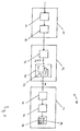
- Fig. 1 illustrates a partial view of a telecommunication device 10 which comprises a digital section 11, an analogue section 12 and a multi DAC (digital-to-analogue converter) arrangement 13 for interfacing between the digital and analogue sections 11, 12.
- the digital and analogue sections 11, 12 can contain any components typically included in a conventional telecommunication device 10.
- the digital section 11 can include a data processor 14 such as a DSP (Digital Signal Processor), an ASIC (Application Specific Integrated Circuit) and/or a FPGA (Field Programmable Gate Array).
- the digital section 11 of the telecommunication device 10 typically comprises a digital radio circuit 15 such as a digital frequency up-converter. This digital radio circuit 15 may also be implemented as part of the DSP.
- the analogue section 12 can include a filter 16, a power amplifier 17 and an output device 18.
- the analogue section 12 may also comprise other components, such as up-conversion circuits if for example frequency up-conversion is not performed by the digital section 11.
- the output device 18 comprises an antenna array 19 having a plurality of antenna elements for transmitting analog signals over the air (OTA) from the telecommunication device 10 to receiver devices, for example within a base station, a user equipment and the like.
- the output circuit 18 may comprise an array of output terminals.
- the multi DAC arrangement 13 is configured to convert between digital signals from the digital section 11 to corresponding analogue signals towards the analogue section 12.
- the multi DAC arrangement 13 comprises a DAC array 20 having a plurality of single DACs 21, which hereinafter are also referred to as DAC element 21.
- the plurality of DACs 21 are arranged in parallel to each other for converting a digital signal from the digital section 11 to an analogue signal provided to the analogue section 12.
- each DAC path has a different analogue phase response. This can be achieved by using multiphase clocking to control operation of the DACs 21.
- the inputs and outputs of the DACs 21 can be delayed (i.e. phase shifted) with respect to each other in order to ensure that each DAC path has a different analogue phase response.
- the multi DAC arrangement 13 further comprises a digital serial interface circuit 22 which is configured to provide a serial data stream X1 to the plurality of DACs 21.
- the digital serial interface circuit 22 further provides control information X2, X3 to each DACs 22.
- This control information X2, X3 comprises on the one hand side synchronization information X2 for synchronization of the different parallel arranged DAC elements 21.
- the control information X2, X3 comprises phase shift information X3 for setting a predefined phase shift for the analogue output data signals provided at the output side of the different DAC elements 21.
- the structure and functionality of the digital serial interface circuit 22 and DAC elements 21 is hereinafter described in more detail with regard to Fig. 2 .
- the digital serial interface circuit 22 may be implemented as part of the data processor 14 which is included in the digital section 11 of the telecommunication device 10. However, the digital serial interface circuit 22 may also be implemented separate from the data processor 14.
- the telecommunication device 10 as a whole or parts of it denote the RF transmit circuit arrangement in the terminology of the present invention.
- Fig. 2 shows a detailed block diagram for the multi DAC arrangement of Fig. 1 .
- the digital serial interface circuit 22 is a JESD204 interface 22 and in particular a JESD204B interface 22.
- the signal stream (data and control signals) produced by the digital serial interface circuit 22 is based on the JESD204 transport protocol standard.
- the converter array 20 comprises an array of M DAC elements 21-1 to 21-M.
- the digital serial interface circuit 22 is configured to provide an N-bit data stream X1-1, X1-2 to each of the DAC elements 21-1, 21-2.
- Each DAC element 21-1, 21-2 is an N-bit DAC 21-1, 21-2 which is configured to convert an N-bit digital signal X1-1, X1-2 into a corresponding analogue output signal X4-1, X4-2.
- each DAC element 21-1, 21-2 comprises at its input interface a de-serializer 23-1, 23-2.
- This de-serializer 23-1, 23-2 is configured to convert the N-bit serial data stream X1-1, X1-2 in N different input signals which are provided to respective internal input terminals of the DAC element 21-1, 21-2.
- the digital serial interface circuit 22 is further configured to provide a synchronization signal X2-1, X2-2 to each DAC element 21-1, 21-2.
- This synchronization signal X2-1, X2-2 is used for synchronization of the different DAC elements 21-1, 21-2 within the converter array 20.
- each of the DAC elements 21-1, 21-2 of the converter array 20 comprises an independent internal numerically controlled oscillator (NCO) 24-1, 24-2.
- NCO numerically controlled oscillator
- This carrier signal is then used as a carrier for the data which is modulated on the carrier signal.
- the digital serial interface circuit 22 provides a control signal X3-1, X3-2 to the NCO 24-1, 24-2.
- This control signal X3-1, X3-2 comprises control and phase shift information. If these control and phase shift information are provided to the corresponding NCOs 24-1, 24-2 of different DAC elements 21-1, 21-2, then the analogue output signals X4-1, X4-2 produced by the DAC elements 21-1, 21-2 comprise a predefined phase shift to each other. This relationship is illustrated in Fig. 3 .
- the generated analogue output signals X4-1, X4-2 are then forwarded to the antennas of the output device 18.
- so-called smart antennas are used within the antenna array 19.
- Smart antennas are arrays of antenna elements, wherein each of these antenna elements receive an analogue signal X4-1, X4-2 to be transmitted with a predetermined phase offset and a relative gain.
- the net effect of the antenna array 19 is to direct a transmit beam in a predefined direction.
- the beam is steered and formed by controlling the phase and gain relationships of the signals that excite the antenna elements of the antenna array 19.
- Fig. 3 shows a signal-time diagram for illustrating the phase shift between the transmit signals generated by two different DACs of the RF transmit circuit arrangement of Fig. 2 .
- Two analogue RF data signals X4-1, X4-2 are produced by the two DAC elements 21-1, 21-2 of Fig. 2 .
- the two analogue RF data signals X4-1, X4-2 have a predefined phase shift X5 to each other.
- This predefined phase shift is set and controlled via the phase shift information comprised within the control signals X3-1, X3-2 provided to the corresponding DAC elements 21-1, 21-2.
- This way, according to the present invention it is possible to transfer digital data with a predefined phase shift from the digital side to the analogue side of a DAC array 20. In particular, only one control information per sample is needed for each NCO 24-1, 24-2.
Landscapes
- Engineering & Computer Science (AREA)
- Theoretical Computer Science (AREA)
- Radar, Positioning & Navigation (AREA)
- Remote Sensing (AREA)
- Computer Networks & Wireless Communication (AREA)
- Physics & Mathematics (AREA)
- General Physics & Mathematics (AREA)
- Signal Processing (AREA)
- General Engineering & Computer Science (AREA)
- Variable-Direction Aerials And Aerial Arrays (AREA)
Abstract
Description
- The invention relates to a method for controlling digital-to-analogue converters. The invention further relates to a RF transmit circuit arrangement.
- Wireless communication systems are widely deployed to provide various types of communication contents such as voice, video, data and the like. Transceiver devices for wireless communication systems typically comprise high speed analogue or digital front end (AFE, DFE) devices. These AFE/ DFE devices typically comprise digital processors which are used to perform complex processing while adhering to reasonable power and size constraints. In order to transfer information to another radio device, the data signals are normally first converted into analogue signals which may then be sent by a suitable antenna. The conversion process is performed by digital-to-analogue converters.
- In electronics, a digital-to-analogue converter (DAC, D/A, D-A) is a device that converts a digital signal into an analogue signal. An analogue-to-digital converter (ADC) performs the reverse function. There are specific DAC architectures for different applications. For example, high-speed DACs are used to transmit at high data rates. These DAC types permit moving some of the traditional analogue functionality of a radio system into the digital domain, such as frequency up-conversion. One technique to improve the sampling rate of a DAC system is to use multiple DACs in parallel. A parallel DAC architecture typically includes multiple DACs whose outputs are combined in the analogue domain.
- For high-speed DFE applications, a single DAC element uses an externally generated clock signal. This clock signal is used within the DAC to generate a carrier signal which is then modulated with the transmit data. However, one problem with this approach is a potential misalignment of the different output signals of the DAC elements of a multi DAC array with regard to their phase shift. As a consequence of this, the clock generators which are triggering the DAC elements have to be reset regularly and sometimes for each data sample in order to ensure a predefined phase shift. However, for high-speed applications, in particular for wireless RF data communication, this resetting is decreasing the data throughput significantly.
- A predefined phase shift is in particular essential for beamforming. Beamforming is used for transmitting RF signals in order to generate a predefined beam form. With the beamforming technique, so-called smart multiple antennas are used. Smart antennas are arrays of antenna elements, wherein each of these antenna elements receive an analogue signal from a DAC. This analogue signals are to be transmitted with a predetermined phase offset and a relative gain. The net effect of the array is to direct a transmit beam in a predefined direction. The beam is steered by controlling the phase and gain relationships of the signals that excite the antenna elements of the array. However, in case, that the different transmit signals are not sent at a predefined point of time from the different antenna elements, it will be nearly impossible to obtain a predefined form of the beam.
-
US 8,286,067 B2 describes a method for transmitting sampled data and control information between a digital signal processor and an RF analogue front end device. The analogue front end device comprises two DACs within the transmit path. The clock signal for triggering these DACs is generated externally. For a given clock rate, the serial interface transmitter of the analogue front end device provides variable data rates by inserting null frames to match the data rate to the clock rate. The null frames may be identified by specific codes within the control field. Thus,US 8,286,067 B2 discloses a method for controlling multiple DACs within a modem, wherein the control data for controlling the DACs is included within the transmitted data. - Against this background, the problem addressed by the present invention is to provide a stable phase difference between the output signals of the DAC elements of a DAC array.
- According to the invention this problem is solved by a method having the features of claim 1 and/or by a RF transmit circuit arrangement having the features of claim 8.
- According thereto, the following is provided:
- A method for controlling digital-to-analogue converters (DAC), the method comprising: providing a plurality of digital-to-analogue converters (DAC) of a multi-channel converter array wherein each DAC includes a separate clock generator; generating, by each clock generator, a RF carrier signal; converting, by each DAC, digital data signals into analogue RF data signals based on the carrier signals of the corresponding clock generators; providing a separate control signal for each clock generator wherein the control signals comprise control information such that when the control signals are applied to the corresponding clock generators the different analogue RF data signals provided at respective output terminals of each DAC comprise a pre-defined phase shift to each other; controlling the clock generator of each DAC directly and independently (i.e. individually) based on the provided control signals.
- A RF transmit circuit arrangement, comprising: a digital interface circuit; a multi-channel converter array coupled on its digital input side to the digital interface circuit and having a plurality of digital-to-analogue converters (DAC) wherein each DAC includes a separate clock generator and wherein each DAC is configured to convert digital data signals provided by the digital interface circuit into analogue RF data signals; wherein the digital interface circuit further comprises a control circuit which is configured to provide control signals for controlling the clock generators of each DAC directly and independently (i.e. individually) and wherein each control signal comprises control information such that the different analogue RF data signals provided at respective output terminals of each DAC comprise a predefined phase shift to each other.
- The present invention is based on the finding that analogue RF output signals which are provided at the output of a DAC array compulsory need a stable phase shift to each other for specific applications, in particular for time division multiplex applications, for beamforming or the like.
- For this purpose, a first idea of the present invention is to shift the functionality of the clock generation inside every individual DAC element such that every DAC element is generating the carrier signal based on an internally generated clock signal. According to a second idea of the present invention each clock generator within a DAC element is triggered independently by a separate control signal. This control signal comprises phase shift information for the corresponding and is generated by the digital interface circuit. As a consequence, the different DAC elements within the DAC array are each triggered by separate control signals such that the corresponding analogue RF output signals which are provided on the respective output terminals of each DAC element comprise a predefined phase shift to each other.
- With the present invention it is possible to synchronize the different digital channels such that they are operating with a predefined phase shift sample exact to each other.
- Additionally, by using only one control signal for each DAC element it is possible to provide a very smart and easy approach for synchronizing the RF output signals generated by the DAC elements. This way, it is possible to provide predefined phasing of the RF output signals with the consequence that specific applications like beamforming are possible also for high speed applications.
- Further, by employing individual control information for each clock generator separately, resetting the clock generators is avoided. By not resetting the clock generators regularly, the present invention is suitable for high performance and high speed applications.
- Advantageous configurations and developments emerge from the further depending claims and from the description with reference to the figures of the drawings.
- In one preferred embodiment, the analogue RF data signals which are generated by the multi-channel converter array and which are provided at respective output terminals of the DAC are each forwarded to antenna elements of an antenna array. This antenna array is then transmitting over the air RF signals based on the analogue RF data signals.
- In a particular preferred embodiment, the method is used for beamforming by setting a predefined shape of the beam. This predefined shape within the beam may be set via the control information of the control signal. Beamforming can be applied for radio or sound waves. Beamforming has various applications in radar, sonar, wireless communication, acoustics and biomedicine. For beamforming applications, typically a phased antenna array is used. A phased antenna array is an array of antennas in which the relative phases of the respective signals which are feeding the antennas are set in such a way that the effective radiation pattern of the array is reinforced in a desired direction and suppressed in undesired directions. It is very essential for those phased antenna arrays, that the phase relationships among the antennas may be fixed. In this case, however, it is essential to provide pre-defined phase shifts between the different analogue signals feeding the antenna elements. The present invention which provides such predefined phase shifts which enables a very smart beamforming technique.
- In a particular preferred embodiment, the digital interface circuit is a JESD204 interface, in particular a JESD204B interface. Consequently, the digital data signals which are fed into the DACs of the RF converter array and the control signals which are supplied to the DAC and their NCOs, respectively, are generated based on the JESD204 or specifically on the JESD204B transport protocol standard. As the resolution and speed of ADCs and DACs has increased in recent times, the demand for a more efficient interface has grown. The JESD204 interface brings this efficiency and offers several advantages over CMOS and LVDS interfaces in terms of speed, size and cost. JESD refers to a data interface that is able to support the high bandwidth necessary for high performance, high speed and multi-channel applications. In addition, with JESD204 there is a significant reduction in input-output terminals which leads to smaller package sizes while reducing the number of digital input-outputs (IO) needed. Consequently, the JESD204 interface standard is easing board layout and circuitry. Very high speed ADCs and DACs, which are for example used for RF communication that would have previously required a complex interface design using a large number of FPGAs are now implemented within just a few IOs terminals. The total bandwidth of the JESD204 interface can also be separated into multi-channels based on the requirements of the application again without requiring additional IOs.
- In a particular preferred embodiment, the method further comprises the steps of coding an information of the starting phase, an increment and a point of time of switching into the control signal. The DAC is then analyzing this information. Based on the analyzed information, the clock generator of the DAC is switched. This switching may be conducted sample exact. This means, that each clock generator of a DAC is controlled sample exact with regard to the data samples of the digital data signals provided to the corresponding DAC.
- In a particular preferred embodiment, at least one control information per sample of the data signals is provided to each clock generator.
- In a particular preferred embodiment, each DAC is individually synchronized with regard to the frequency and phase of the carrier signal. Additionally, or alternatively, each DAC is individually and independently synchronized with regard to the analogue RF data signals. In particular, the controlling and/or synchronizing of the clock generators of each DAC is directly, individually and independently performed without resetting the clock generators.
- In another embodiment, the digital serial interface circuit is a serial high-speed multi-channel time division multiplexing (TDM) interface.
- In a preferred embodiment, at least one of the clock generators is a numerically controlled oscillator (NCO). A numerically controlled oscillator is a digital signal generator which creates a synchronous (i.e. clocked), discrete-time, discrete-valued representation of a specific waveform of the signal. Usually this specific waveform of the signal is sinusoidal. Numerically controlled oscillators offer several advantages over other types of oscillators in terms of agility, accuracy, stability and reliability. NCOs are very often used in communication systems, in particular for wireless communication, including digital up/down converters, digital PLLs, radar systems, drivers for optical or acoustic transmission, multilevel FSK/PSK modulators, demodulators and the like. Alternatively, the clock generator may also be a digitally controlled oscillator (DCO). A DCO is a hybrid digital/analogue electronic oscillator which is very often used in frequency synthesizers. DCOs are a kind of a voltage controlled oscillator (VCO) and are designed to overcome the tuning stability limitations of early VCO designs.
- In a preferred embodiment, the RF transmit circuit arrangement further comprises an antenna array having a plurality of antenna elements. Each of these antenna elements is connected on their input terminals over data lines to a corresponding output terminal of a DAC. Analogue RF data signals which are generated by the DAC are provided over these data lines to the corresponding antenna elements.
- In a particular preferred embodiment, the RF transmit circuit arrangement is configured to transmit radar signals. Additionally or alternatively, the RF transmit circuit arrangement is configured to transmit high speed wireless communication signals such as in particular according to the LTE or 5G standard.
- In one embodiment, the digital serial interface circuit is connected for the RF data transmission to each DAC via a plurality of data lines. Further, the digital serial interface circuit is connected to each DAC via a first control line for synchronizing the DACs with each other and via a second control line to the NCO for setting the predefined phase shift. Additionally, the RF transmit circuit arrangement comprises a digital input side coupled to the digital serial interface circuit and an analogue output side at the output of the converter arrangement.
- Where appropriate, the above-mentioned configurations and developments can be combined in any suitable manner. Further possible configurations, developments and implementations of the invention also include combinations, which are not explicitly mentioned, of features of the invention which have been described previously or are described in the following with reference to the embodiments. In particular, in this case, a person skilled in the art will also add individual aspects as improvements or supplements to the basic form of the present invention.
- The present invention is described in greater detail in the following on the basis of the embodiments shown in the schematic figures of the drawings, in which:
- Fig. 1
- illustrates a partial view of a telecommunication device which comprises a multi DAC arrangement according to the invention for interfacing between a digital section and an analogue section;
- Fig. 2
- is a detailed block diagram for the multi DAC arrangement of
Fig. 1 ; - Fig. 3
- is a signal-time diagram for illustrating the phase shift between two transmit signals generated by different DACs of the RF transmit circuit arrangement of
Fig. 2 . - The appended drawings are intended to provide further understanding of the embodiments of the invention. They illustrate embodiments and, in conjunction with the description, help to explain principles and concepts of the invention. Other embodiments and many of the advantages mentioned become apparent in view of the drawings. The elements in the drawings are not necessarily shown to scale.
- In the drawings, like, functionally equivalent and identically operating elements, features and components are provided with like reference signs in each case, unless stated otherwise.
- As a non-limiting example,
Fig. 1 illustrates a partial view of a telecommunication device 10 which comprises adigital section 11, ananalogue section 12 and a multi DAC (digital-to-analogue converter)arrangement 13 for interfacing between the digital andanalogue sections analogue sections digital section 11 can include a data processor 14 such as a DSP (Digital Signal Processor), an ASIC (Application Specific Integrated Circuit) and/or a FPGA (Field Programmable Gate Array). Thedigital section 11 of the telecommunication device 10 typically comprises adigital radio circuit 15 such as a digital frequency up-converter. Thisdigital radio circuit 15 may also be implemented as part of the DSP. - The
analogue section 12 can include a filter 16, apower amplifier 17 and anoutput device 18. Theanalogue section 12 may also comprise other components, such as up-conversion circuits if for example frequency up-conversion is not performed by thedigital section 11. Theoutput device 18 comprises an antenna array 19 having a plurality of antenna elements for transmitting analog signals over the air (OTA) from the telecommunication device 10 to receiver devices, for example within a base station, a user equipment and the like. Alternatively, theoutput circuit 18 may comprise an array of output terminals. - The
multi DAC arrangement 13 is configured to convert between digital signals from thedigital section 11 to corresponding analogue signals towards theanalogue section 12. For this purpose, themulti DAC arrangement 13 comprises aDAC array 20 having a plurality ofsingle DACs 21, which hereinafter are also referred to asDAC element 21. The plurality ofDACs 21 are arranged in parallel to each other for converting a digital signal from thedigital section 11 to an analogue signal provided to theanalogue section 12. Typically, each DAC path has a different analogue phase response. This can be achieved by using multiphase clocking to control operation of theDACs 21. In particular, the inputs and outputs of the DACs 21 can be delayed (i.e. phase shifted) with respect to each other in order to ensure that each DAC path has a different analogue phase response. - The
multi DAC arrangement 13 further comprises a digitalserial interface circuit 22 which is configured to provide a serial data stream X1 to the plurality ofDACs 21. The digitalserial interface circuit 22 further provides control information X2, X3 to each DACs 22. This control information X2, X3 comprises on the one hand side synchronization information X2 for synchronization of the different parallel arrangedDAC elements 21. On the other hand side the control information X2, X3 comprises phase shift information X3 for setting a predefined phase shift for the analogue output data signals provided at the output side of thedifferent DAC elements 21. The structure and functionality of the digitalserial interface circuit 22 andDAC elements 21 is hereinafter described in more detail with regard toFig. 2 . - The digital
serial interface circuit 22 may be implemented as part of the data processor 14 which is included in thedigital section 11 of the telecommunication device 10. However, the digitalserial interface circuit 22 may also be implemented separate from the data processor 14. - The telecommunication device 10 as a whole or parts of it denote the RF transmit circuit arrangement in the terminology of the present invention.
-
Fig. 2 shows a detailed block diagram for the multi DAC arrangement ofFig. 1 . Here, the digitalserial interface circuit 22 is aJESD204 interface 22 and in particular aJESD204B interface 22. Thus, the signal stream (data and control signals) produced by the digitalserial interface circuit 22 is based on the JESD204 transport protocol standard. - The
converter array 20 comprises an array of M DAC elements 21-1 to 21-M. In the present case, theconverter array 20 comprises M=2 DAC elements 21-1, 21-2. - The digital
serial interface circuit 22 is configured to provide an N-bit data stream X1-1, X1-2 to each of the DAC elements 21-1, 21-2. - Each DAC element 21-1, 21-2is an N-bit DAC 21-1, 21-2 which is configured to convert an N-bit digital signal X1-1, X1-2 into a corresponding analogue output signal X4-1, X4-2. For this purpose, each DAC element 21-1, 21-2 comprises at its input interface a de-serializer 23-1, 23-2. This de-serializer 23-1, 23-2 is configured to convert the N-bit serial data stream X1-1, X1-2 in N different input signals which are provided to respective internal input terminals of the DAC element 21-1, 21-2.
- The digital
serial interface circuit 22 is further configured to provide a synchronization signal X2-1, X2-2 to each DAC element 21-1, 21-2. This synchronization signal X2-1, X2-2 is used for synchronization of the different DAC elements 21-1, 21-2 within theconverter array 20. - According to one aspect of the present invention, each of the DAC elements 21-1, 21-2 of the
converter array 20 comprises an independent internal numerically controlled oscillator (NCO) 24-1, 24-2. This NCO is used to generate a carrier signal. Within the corresponding DAC 21-1, 21-2 this carrier signal is then used as a carrier for the data which is modulated on the carrier signal. - According to a further aspect of the present invention, the digital
serial interface circuit 22 provides a control signal X3-1, X3-2 to the NCO 24-1, 24-2. This control signal X3-1, X3-2 comprises control and phase shift information. If these control and phase shift information are provided to the corresponding NCOs 24-1, 24-2 of different DAC elements 21-1, 21-2, then the analogue output signals X4-1, X4-2 produced by the DAC elements 21-1, 21-2 comprise a predefined phase shift to each other. This relationship is illustrated inFig. 3 . - The generated analogue output signals X4-1, X4-2 are then forwarded to the antennas of the
output device 18. With the beamforming technique, so-called smart antennas are used within the antenna array 19. Smart antennas are arrays of antenna elements, wherein each of these antenna elements receive an analogue signal X4-1, X4-2 to be transmitted with a predetermined phase offset and a relative gain. The net effect of the antenna array 19 is to direct a transmit beam in a predefined direction. The beam is steered and formed by controlling the phase and gain relationships of the signals that excite the antenna elements of the antenna array 19. -
Fig. 3 shows a signal-time diagram for illustrating the phase shift between the transmit signals generated by two different DACs of the RF transmit circuit arrangement ofFig. 2 . - Two analogue RF data signals X4-1, X4-2 are produced by the two DAC elements 21-1, 21-2 of
Fig. 2 . The two analogue RF data signals X4-1, X4-2 have a predefined phase shift X5 to each other. This predefined phase shift is set and controlled via the phase shift information comprised within the control signals X3-1, X3-2 provided to the corresponding DAC elements 21-1, 21-2. This way, according to the present invention, it is possible to transfer digital data with a predefined phase shift from the digital side to the analogue side of aDAC array 20. In particular, only one control information per sample is needed for each NCO 24-1, 24-2. - Although the present invention has been described in the above by way of preferred embodiments, it is not limited thereto, but rather can be modified in a wide range of ways. In particular, the invention can be changed or modified in various ways without deviating from the core of the invention.
-
- 10
- telecommunication device, RF transmit circuit arrangement
- 11
- digital section
- 12
- analogue section
- 13
- multi DAC system/arrangement
- 14
- data processor, DSP
- 15
- digital radio circuit
- 16
- filter
- 17
- power amplifier
- 18
- output device, output circuit
- 19
- antenna array
- 20
- DAC array
- 21, 21-1, 21-2
- digital-to analogue converter, DAC, DAC element
- 22
- digital serial interface circuitry
- 23-1, 23-2
- de-serializer
- 24-1, 24-2
- clock generator, numerically controlled oscillator, NCO
- X1, X1-1, X1-2
- data stream, serial data signal
- X2, X2-1, X2-2
- synchronization signal
- X3, X3-1, X3-2
- control signal
- X4, X4-1, X4-2
- analogue RF data signal
- X5
- phase shift
Claims (14)
- A method for controlling digital-to-analogue converters (DAC), the method comprising:providing a plurality of digital-to-analogue converters (DAC) of a multi-channel converter array wherein each DAC includes a separate clock generator;generating, by each clock generator, a RF carrier signal;converting, by each DAC, digital data signals into analogue RF data signals based on the carrier signals of the corresponding clock generators;providing a separate control signal for each clock generator wherein the control signals comprise control information such that when the control signals are applied to the corresponding clock generators the different analogue RF data signals provided at respective output terminals of each DAC comprise a predefined phase shift to each other;controlling the clock generator of each DAC directly and independently based on the provided control signals.
- The method according to claim 1,
wherein the generated analogue RF data signals are each provided to antenna elements of an antenna array. - The method according to any of the preceding claims, wherein the method is used for beamforming.
- The method according to any of the preceding claims, wherein the data signals and/or control signals are based on the JESD204 transport protocol standard, in particular based on the JESD204B transport protocol standard.
- The method according to any of the preceding claims, further comprising:- coding an information of the starting phase, an increment and a point of time of switching into the control signal;- analysing this information by the corresponding DAC;- sample exact switching the clock generator of the corresponding DAC based on the analysed information.
- The method according to any of the preceding claims, wherein at least one control information per sample is provided to each clock generator.
- The method according to any of the preceding claims, wherein each DAC is individually synchronized with regard to the frequency and phase of the carrier signal and/or the analogue RF data signals.
- A RF transmit circuit arrangement, comprising:a digital serial interface circuit;a multi-channel converter array coupled on its digital input side to the digital interface circuit and having a plurality of digital-to-analogue converters (DAC) wherein each DAC includes a separate clock generator and wherein each DAC is configured to convert digital data signals provided by the digital serial interface circuit into analogue RF data signals;wherein the digital serial interface circuit further comprises a control circuit which is configured to provide control signals for controlling the clock generators of each DAC directly and independently and wherein each control signal comprises control information such that the different analogue RF data signals provided at respective output terminals of each DAC comprise a predefined phase shift to each other.
- The arrangement according to claims 8,
wherein the digital serial interface circuit is a JESD204 interface, in particular a JESD204B interface. - The arrangement according to claims 8 or 9,
wherein at least one clock generator is a numerically controlled oscillator (NCO) and/or digitally controlled oscillator (DCO). - The arrangement according to claims 8 to 10,
wherein the RF transmit circuit arrangement is used for beamforming of the wirelessly transmitted RF data signals. - The arrangement according to claims 8 to 11,
further comprising an antenna array having a plurality of antenna elements, wherein each antenna element is connected on their input terminals to a corresponding output terminal of a DAC to provide the analogue RF data signals to the corresponding antenna elements. - The arrangement according to claims 8 to 12,
wherein the RF transmit circuit arrangement is configured to transmit radar signals and/or high speed wireless communication signals, in particular according to the LTE or 5G standard. - The arrangement according to claims 8 to 13,
wherein the digital serial interface circuit is connected to each of the DACs via a plurality of data lines for the RF data transmission and via a first control line for synchronizing the DAC with each other and via a second control line for setting the predefined phase shift.
Priority Applications (3)
| Application Number | Priority Date | Filing Date | Title |
|---|---|---|---|
| EP16190818.1A EP3300256B1 (en) | 2016-09-27 | 2016-09-27 | Method for controlling digital-to-analogue converters and rf transmit circuit arrangement |
| US15/603,621 US10333603B2 (en) | 2016-09-27 | 2017-05-24 | Method for controlling digital-to-analogue converters and RF transmit circuit arrangement |
| CN201710549140.8A CN107872228B (en) | 2016-09-27 | 2017-07-10 | Method for controlling digital-to-analog converter and RF transmitting circuit arrangement |
Applications Claiming Priority (1)
| Application Number | Priority Date | Filing Date | Title |
|---|---|---|---|
| EP16190818.1A EP3300256B1 (en) | 2016-09-27 | 2016-09-27 | Method for controlling digital-to-analogue converters and rf transmit circuit arrangement |
Publications (2)
| Publication Number | Publication Date |
|---|---|
| EP3300256A1 true EP3300256A1 (en) | 2018-03-28 |
| EP3300256B1 EP3300256B1 (en) | 2021-06-02 |
Family
ID=57067959
Family Applications (1)
| Application Number | Title | Priority Date | Filing Date |
|---|---|---|---|
| EP16190818.1A Active EP3300256B1 (en) | 2016-09-27 | 2016-09-27 | Method for controlling digital-to-analogue converters and rf transmit circuit arrangement |
Country Status (3)
| Country | Link |
|---|---|
| US (1) | US10333603B2 (en) |
| EP (1) | EP3300256B1 (en) |
| CN (1) | CN107872228B (en) |
Cited By (1)
| Publication number | Priority date | Publication date | Assignee | Title |
|---|---|---|---|---|
| CN111865461A (en) * | 2020-05-25 | 2020-10-30 | 北京无线电测量研究所 | Broadband multichannel digital TR circuit |
Families Citing this family (10)
| Publication number | Priority date | Publication date | Assignee | Title |
|---|---|---|---|---|
| US20190273524A1 (en) * | 2018-03-05 | 2019-09-05 | Maxlinear, Inc. | Methods and systems for utilizing ultra-efficiency low noise configurations for phased array antennas |
| DE102018121353A1 (en) * | 2018-08-31 | 2020-03-05 | Universität Duisburg-Essen | Radio access device and network with fiber optic data transmission and radio access device |
| CN109254939B (en) * | 2018-09-04 | 2020-08-04 | 珠海昇生微电子有限责任公司 | Drive control method and system of digital-analog interface |
| CN109660997B (en) * | 2018-11-26 | 2022-07-08 | 京信网络系统股份有限公司 | Configuration method and device of converter, computer equipment and storage medium |
| EP3660981B8 (en) * | 2018-11-29 | 2021-06-02 | Rohde & Schwarz GmbH & Co. KG | Spatial and bandwidth multiplexing device and method |
| EP3696625B1 (en) * | 2019-02-15 | 2022-04-13 | Siemens Aktiengesellschaft | Analog installation module |
| CN110658884B (en) * | 2019-09-24 | 2021-01-15 | 浪潮集团有限公司 | A method and system for waveform synchronization of multi-channel signal generator based on FPGA |
| CN111831055B (en) * | 2020-07-17 | 2023-01-17 | 南京典格通信科技有限公司 | JESD interface common package design method based on multiple sampling rates in FPGA |
| CN115149950B (en) * | 2021-03-30 | 2024-06-04 | 西南电子技术研究所(中国电子科技集团公司第十研究所) | Large-scale subarray digital array multichannel synchronous sampling system |
| KR102926950B1 (en) * | 2023-07-21 | 2026-02-12 | 주식회사 셀트론 | Signal generator |
Citations (3)
| Publication number | Priority date | Publication date | Assignee | Title |
|---|---|---|---|---|
| US7394424B1 (en) * | 2005-11-04 | 2008-07-01 | Raytheon Company | Methods and apparatus for implementing a wideband digital beamforming network |
| US20080240170A1 (en) * | 2007-03-29 | 2008-10-02 | Mostafa Elmala | Systems and methods for digital delayed array transmitter architecture with beam steering capability for high data rate |
| US8286067B2 (en) | 2009-02-05 | 2012-10-09 | Analog Devices, Inc. | Method for transmitting sampled data and control information between a DSP and an RF/analog front-end |
Family Cites Families (7)
| Publication number | Priority date | Publication date | Assignee | Title |
|---|---|---|---|---|
| US5815046A (en) * | 1997-02-11 | 1998-09-29 | Stanford Telecom | Tunable digital modulator integrated circuit using multiplexed D/A converters |
| WO2002069443A1 (en) * | 2001-02-28 | 2002-09-06 | Itt Manufacturing Enterprises, Inc. | Integrated beamformer/method architecture |
| JP4423454B2 (en) * | 2005-08-26 | 2010-03-03 | テクトロニクス・インターナショナル・セールス・ゲーエムベーハー | Signal generator |
| US8565345B2 (en) * | 2005-10-04 | 2013-10-22 | Hypres Inc. | Oversampling digital radio frequency transmitter |
| US8592697B2 (en) * | 2008-09-10 | 2013-11-26 | Apple Inc. | Single-chip multi-stimulus sensor controller |
| US8779867B2 (en) * | 2011-10-26 | 2014-07-15 | Intel Mobile Communications GmbH | Split varactor array with improved matching and varactor switching scheme |
| CN105871378A (en) * | 2016-03-24 | 2016-08-17 | 航天科技控股集团股份有限公司 | A synchronous circuit of multi-channel high-speed ADC and DAC |
-
2016
- 2016-09-27 EP EP16190818.1A patent/EP3300256B1/en active Active
-
2017
- 2017-05-24 US US15/603,621 patent/US10333603B2/en active Active
- 2017-07-10 CN CN201710549140.8A patent/CN107872228B/en active Active
Patent Citations (3)
| Publication number | Priority date | Publication date | Assignee | Title |
|---|---|---|---|---|
| US7394424B1 (en) * | 2005-11-04 | 2008-07-01 | Raytheon Company | Methods and apparatus for implementing a wideband digital beamforming network |
| US20080240170A1 (en) * | 2007-03-29 | 2008-10-02 | Mostafa Elmala | Systems and methods for digital delayed array transmitter architecture with beam steering capability for high data rate |
| US8286067B2 (en) | 2009-02-05 | 2012-10-09 | Analog Devices, Inc. | Method for transmitting sampled data and control information between a DSP and an RF/analog front-end |
Non-Patent Citations (1)
| Title |
|---|
| GEORGE DINIZ: "Using JESD204B for wideband data converter apps", 1 January 2012 (2012-01-01), pages 1 - 4, XP055349210, Retrieved from the Internet <URL:https://www.google.nl/url?sa=t&rct=j&q=&esrc=s&source=web&cd=1&ved=0ahUKEwiq5fm3qqjSAhWrCsAKHf2EC4YQFggpMAA&url=http%3A%2F%2Fwww.eetasia.com%2FSTATIC%2FPDF%2F201211%2FEEOL_2012NOV29_AMP_INT_TA_01.pdf%3FSOURCES%3DDOWNLOAD&usg=AFQjCNH0KUv3QBXpPMM4fHDxpFkrtzmevQ&sig2=qJ9YoUK4fiB3st6qLRuZcA&cad=rja> [retrieved on 20170223] * |
Cited By (1)
| Publication number | Priority date | Publication date | Assignee | Title |
|---|---|---|---|---|
| CN111865461A (en) * | 2020-05-25 | 2020-10-30 | 北京无线电测量研究所 | Broadband multichannel digital TR circuit |
Also Published As
| Publication number | Publication date |
|---|---|
| US20180091203A1 (en) | 2018-03-29 |
| CN107872228B (en) | 2023-05-02 |
| US10333603B2 (en) | 2019-06-25 |
| CN107872228A (en) | 2018-04-03 |
| EP3300256B1 (en) | 2021-06-02 |
Similar Documents
| Publication | Publication Date | Title |
|---|---|---|
| US10333603B2 (en) | Method for controlling digital-to-analogue converters and RF transmit circuit arrangement | |
| KR101829974B1 (en) | System and method for high-speed analog beamforming | |
| EP2965430B1 (en) | Configurable time-interleaved analog-to-digital converter | |
| EP3889636A1 (en) | Radar system and control method therefor | |
| KR20110108362A (en) | System and Method for Improved Digital RF Transmission in Distributed Antenna Systems | |
| JP2010530150A (en) | Signal processing system | |
| EP1266427B1 (en) | Digital phased array architecture and associated method | |
| WO2016051710A1 (en) | Digital modulation device, and digital modulation method | |
| KR20180072765A (en) | Beam forming engine | |
| JP6876191B2 (en) | Multi-functional channelization / DDC architecture for digital receivers / exciters | |
| JP2017055245A (en) | Transceiver module and active phased array antenna | |
| US9065472B1 (en) | Multi-function reconfigurable delta sigma DAC | |
| EP2109937B1 (en) | A digital multi-channel system for processing radio signals, in particular of the very wide band type | |
| US20080191913A1 (en) | Circuit and method for a/d conversion processing and demodulation device | |
| JP2001085925A (en) | Wireless communication system | |
| EP3751754B1 (en) | Satellite receiver and satellite communication system | |
| US7705764B2 (en) | Method of algorithmic analog-to-digital conversion and algorithmic analog-to-digital converter | |
| JP4711892B2 (en) | Multi-antenna communication device | |
| Akram et al. | Massive-MIMO and digital mm-wave arrays on RF-SoCs using FDM for M-fold increase in antennas per ADC/DAC | |
| US20070011482A1 (en) | Clock generator, radio receiver using the same, function system, and sensing system | |
| US20240396579A1 (en) | Systems And Methods For Electronically Scanned Array Antennas | |
| CN111245489A (en) | Space and bandwidth multiplexing device and method | |
| US7751787B2 (en) | Timing generator and methods thereof | |
| JP5358676B2 (en) | Filter circuit, transmission filter circuit, semiconductor integrated circuit, communication device, and timing adjustment method for filter circuit | |
| US11522287B2 (en) | Active phased array antenna |
Legal Events
| Date | Code | Title | Description |
|---|---|---|---|
| PUAI | Public reference made under article 153(3) epc to a published international application that has entered the european phase |
Free format text: ORIGINAL CODE: 0009012 |
|
| STAA | Information on the status of an ep patent application or granted ep patent |
Free format text: STATUS: THE APPLICATION HAS BEEN PUBLISHED |
|
| AK | Designated contracting states |
Kind code of ref document: A1 Designated state(s): AL AT BE BG CH CY CZ DE DK EE ES FI FR GB GR HR HU IE IS IT LI LT LU LV MC MK MT NL NO PL PT RO RS SE SI SK SM TR |
|
| AX | Request for extension of the european patent |
Extension state: BA ME |
|
| STAA | Information on the status of an ep patent application or granted ep patent |
Free format text: STATUS: REQUEST FOR EXAMINATION WAS MADE |
|
| 17P | Request for examination filed |
Effective date: 20180604 |
|
| RBV | Designated contracting states (corrected) |
Designated state(s): AL AT BE BG CH CY CZ DE DK EE ES FI FR GB GR HR HU IE IS IT LI LT LU LV MC MK MT NL NO PL PT RO RS SE SI SK SM TR |
|
| STAA | Information on the status of an ep patent application or granted ep patent |
Free format text: STATUS: EXAMINATION IS IN PROGRESS |
|
| 17Q | First examination report despatched |
Effective date: 20200330 |
|
| RIC1 | Information provided on ipc code assigned before grant |
Ipc: H01Q 3/26 20060101ALI20201210BHEP Ipc: G06F 1/10 20060101ALI20201210BHEP Ipc: H03M 1/06 20060101AFI20201210BHEP Ipc: H03M 1/66 20060101ALN20201210BHEP |
|
| GRAP | Despatch of communication of intention to grant a patent |
Free format text: ORIGINAL CODE: EPIDOSNIGR1 |
|
| RIC1 | Information provided on ipc code assigned before grant |
Ipc: H03M 1/06 20060101AFI20201214BHEP Ipc: H03M 1/66 20060101ALN20201214BHEP Ipc: G06F 1/10 20060101ALI20201214BHEP Ipc: H01Q 3/26 20060101ALI20201214BHEP |
|
| STAA | Information on the status of an ep patent application or granted ep patent |
Free format text: STATUS: GRANT OF PATENT IS INTENDED |
|
| INTG | Intention to grant announced |
Effective date: 20210121 |
|
| GRAS | Grant fee paid |
Free format text: ORIGINAL CODE: EPIDOSNIGR3 |
|
| GRAA | (expected) grant |
Free format text: ORIGINAL CODE: 0009210 |
|
| STAA | Information on the status of an ep patent application or granted ep patent |
Free format text: STATUS: THE PATENT HAS BEEN GRANTED |
|
| AK | Designated contracting states |
Kind code of ref document: B1 Designated state(s): AL AT BE BG CY CZ DE DK EE ES FI FR GB GR HR HU IS IT LT LU LV MC MK MT NL NO PL PT RO RS SE SI SK SM TR |
|
| RBV | Designated contracting states (corrected) |
Designated state(s): AL AT BE BG CY CZ DE DK EE ES FI FR GB GR HR HU IS IT LT LU LV MC MK MT NL NO PL PT RO RS SE SI SK SM TR |
|
| REG | Reference to a national code |
Ref country code: GB Ref legal event code: FG4D |
|
| REG | Reference to a national code |
Ref country code: AT Ref legal event code: REF Ref document number: 1399399 Country of ref document: AT Kind code of ref document: T Effective date: 20210615 |
|
| REG | Reference to a national code |
Ref country code: DE Ref legal event code: R096 Ref document number: 602016058733 Country of ref document: DE |
|
| REG | Reference to a national code |
Ref country code: LT Ref legal event code: MG9D |
|
| PG25 | Lapsed in a contracting state [announced via postgrant information from national office to epo] |
Ref country code: LT Free format text: LAPSE BECAUSE OF FAILURE TO SUBMIT A TRANSLATION OF THE DESCRIPTION OR TO PAY THE FEE WITHIN THE PRESCRIBED TIME-LIMIT Effective date: 20210602 Ref country code: FI Free format text: LAPSE BECAUSE OF FAILURE TO SUBMIT A TRANSLATION OF THE DESCRIPTION OR TO PAY THE FEE WITHIN THE PRESCRIBED TIME-LIMIT Effective date: 20210602 Ref country code: BG Free format text: LAPSE BECAUSE OF FAILURE TO SUBMIT A TRANSLATION OF THE DESCRIPTION OR TO PAY THE FEE WITHIN THE PRESCRIBED TIME-LIMIT Effective date: 20210902 Ref country code: HR Free format text: LAPSE BECAUSE OF FAILURE TO SUBMIT A TRANSLATION OF THE DESCRIPTION OR TO PAY THE FEE WITHIN THE PRESCRIBED TIME-LIMIT Effective date: 20210602 |
|
| REG | Reference to a national code |
Ref country code: NL Ref legal event code: MP Effective date: 20210602 |
|
| REG | Reference to a national code |
Ref country code: AT Ref legal event code: MK05 Ref document number: 1399399 Country of ref document: AT Kind code of ref document: T Effective date: 20210602 |
|
| PG25 | Lapsed in a contracting state [announced via postgrant information from national office to epo] |
Ref country code: LV Free format text: LAPSE BECAUSE OF FAILURE TO SUBMIT A TRANSLATION OF THE DESCRIPTION OR TO PAY THE FEE WITHIN THE PRESCRIBED TIME-LIMIT Effective date: 20210602 Ref country code: GR Free format text: LAPSE BECAUSE OF FAILURE TO SUBMIT A TRANSLATION OF THE DESCRIPTION OR TO PAY THE FEE WITHIN THE PRESCRIBED TIME-LIMIT Effective date: 20210903 Ref country code: PL Free format text: LAPSE BECAUSE OF FAILURE TO SUBMIT A TRANSLATION OF THE DESCRIPTION OR TO PAY THE FEE WITHIN THE PRESCRIBED TIME-LIMIT Effective date: 20210602 Ref country code: NO Free format text: LAPSE BECAUSE OF FAILURE TO SUBMIT A TRANSLATION OF THE DESCRIPTION OR TO PAY THE FEE WITHIN THE PRESCRIBED TIME-LIMIT Effective date: 20210902 Ref country code: RS Free format text: LAPSE BECAUSE OF FAILURE TO SUBMIT A TRANSLATION OF THE DESCRIPTION OR TO PAY THE FEE WITHIN THE PRESCRIBED TIME-LIMIT Effective date: 20210602 Ref country code: SE Free format text: LAPSE BECAUSE OF FAILURE TO SUBMIT A TRANSLATION OF THE DESCRIPTION OR TO PAY THE FEE WITHIN THE PRESCRIBED TIME-LIMIT Effective date: 20210602 |
|
| PG25 | Lapsed in a contracting state [announced via postgrant information from national office to epo] |
Ref country code: AT Free format text: LAPSE BECAUSE OF FAILURE TO SUBMIT A TRANSLATION OF THE DESCRIPTION OR TO PAY THE FEE WITHIN THE PRESCRIBED TIME-LIMIT Effective date: 20210602 Ref country code: ES Free format text: LAPSE BECAUSE OF FAILURE TO SUBMIT A TRANSLATION OF THE DESCRIPTION OR TO PAY THE FEE WITHIN THE PRESCRIBED TIME-LIMIT Effective date: 20210602 Ref country code: PT Free format text: LAPSE BECAUSE OF FAILURE TO SUBMIT A TRANSLATION OF THE DESCRIPTION OR TO PAY THE FEE WITHIN THE PRESCRIBED TIME-LIMIT Effective date: 20211004 Ref country code: NL Free format text: LAPSE BECAUSE OF FAILURE TO SUBMIT A TRANSLATION OF THE DESCRIPTION OR TO PAY THE FEE WITHIN THE PRESCRIBED TIME-LIMIT Effective date: 20210602 Ref country code: RO Free format text: LAPSE BECAUSE OF FAILURE TO SUBMIT A TRANSLATION OF THE DESCRIPTION OR TO PAY THE FEE WITHIN THE PRESCRIBED TIME-LIMIT Effective date: 20210602 Ref country code: EE Free format text: LAPSE BECAUSE OF FAILURE TO SUBMIT A TRANSLATION OF THE DESCRIPTION OR TO PAY THE FEE WITHIN THE PRESCRIBED TIME-LIMIT Effective date: 20210602 Ref country code: CZ Free format text: LAPSE BECAUSE OF FAILURE TO SUBMIT A TRANSLATION OF THE DESCRIPTION OR TO PAY THE FEE WITHIN THE PRESCRIBED TIME-LIMIT Effective date: 20210602 Ref country code: SK Free format text: LAPSE BECAUSE OF FAILURE TO SUBMIT A TRANSLATION OF THE DESCRIPTION OR TO PAY THE FEE WITHIN THE PRESCRIBED TIME-LIMIT Effective date: 20210602 Ref country code: SM Free format text: LAPSE BECAUSE OF FAILURE TO SUBMIT A TRANSLATION OF THE DESCRIPTION OR TO PAY THE FEE WITHIN THE PRESCRIBED TIME-LIMIT Effective date: 20210602 |
|
| REG | Reference to a national code |
Ref country code: DE Ref legal event code: R097 Ref document number: 602016058733 Country of ref document: DE |
|
| PLBE | No opposition filed within time limit |
Free format text: ORIGINAL CODE: 0009261 |
|
| STAA | Information on the status of an ep patent application or granted ep patent |
Free format text: STATUS: NO OPPOSITION FILED WITHIN TIME LIMIT |
|
| PG25 | Lapsed in a contracting state [announced via postgrant information from national office to epo] |
Ref country code: DK Free format text: LAPSE BECAUSE OF FAILURE TO SUBMIT A TRANSLATION OF THE DESCRIPTION OR TO PAY THE FEE WITHIN THE PRESCRIBED TIME-LIMIT Effective date: 20210602 |
|
| 26N | No opposition filed |
Effective date: 20220303 |
|
| REG | Reference to a national code |
Ref country code: BE Ref legal event code: MM Effective date: 20210930 |
|
| PG25 | Lapsed in a contracting state [announced via postgrant information from national office to epo] |
Ref country code: MC Free format text: LAPSE BECAUSE OF FAILURE TO SUBMIT A TRANSLATION OF THE DESCRIPTION OR TO PAY THE FEE WITHIN THE PRESCRIBED TIME-LIMIT Effective date: 20210602 Ref country code: AL Free format text: LAPSE BECAUSE OF FAILURE TO SUBMIT A TRANSLATION OF THE DESCRIPTION OR TO PAY THE FEE WITHIN THE PRESCRIBED TIME-LIMIT Effective date: 20210602 |
|
| PG25 | Lapsed in a contracting state [announced via postgrant information from national office to epo] |
Ref country code: LU Free format text: LAPSE BECAUSE OF NON-PAYMENT OF DUE FEES Effective date: 20210927 Ref country code: IT Free format text: LAPSE BECAUSE OF FAILURE TO SUBMIT A TRANSLATION OF THE DESCRIPTION OR TO PAY THE FEE WITHIN THE PRESCRIBED TIME-LIMIT Effective date: 20210602 Ref country code: BE Free format text: LAPSE BECAUSE OF NON-PAYMENT OF DUE FEES Effective date: 20210930 |
|
| PG25 | Lapsed in a contracting state [announced via postgrant information from national office to epo] |
Ref country code: HU Free format text: LAPSE BECAUSE OF FAILURE TO SUBMIT A TRANSLATION OF THE DESCRIPTION OR TO PAY THE FEE WITHIN THE PRESCRIBED TIME-LIMIT; INVALID AB INITIO Effective date: 20160927 |
|
| PG25 | Lapsed in a contracting state [announced via postgrant information from national office to epo] |
Ref country code: CY Free format text: LAPSE BECAUSE OF FAILURE TO SUBMIT A TRANSLATION OF THE DESCRIPTION OR TO PAY THE FEE WITHIN THE PRESCRIBED TIME-LIMIT Effective date: 20210602 |
|
| PG25 | Lapsed in a contracting state [announced via postgrant information from national office to epo] |
Ref country code: MK Free format text: LAPSE BECAUSE OF FAILURE TO SUBMIT A TRANSLATION OF THE DESCRIPTION OR TO PAY THE FEE WITHIN THE PRESCRIBED TIME-LIMIT Effective date: 20210602 |
|
| PG25 | Lapsed in a contracting state [announced via postgrant information from national office to epo] |
Ref country code: MT Free format text: LAPSE BECAUSE OF FAILURE TO SUBMIT A TRANSLATION OF THE DESCRIPTION OR TO PAY THE FEE WITHIN THE PRESCRIBED TIME-LIMIT Effective date: 20210602 |
|
| P01 | Opt-out of the competence of the unified patent court (upc) registered |
Free format text: CASE NUMBER: UPC_APP_414875/2023 Effective date: 20230525 |
|
| PGFP | Annual fee paid to national office [announced via postgrant information from national office to epo] |
Ref country code: DE Payment date: 20250919 Year of fee payment: 10 |
|
| PGFP | Annual fee paid to national office [announced via postgrant information from national office to epo] |
Ref country code: GB Payment date: 20250923 Year of fee payment: 10 |
|
| PGFP | Annual fee paid to national office [announced via postgrant information from national office to epo] |
Ref country code: FR Payment date: 20250926 Year of fee payment: 10 |
|
| PG25 | Lapsed in a contracting state [announced via postgrant information from national office to epo] |
Ref country code: TR Free format text: LAPSE BECAUSE OF FAILURE TO SUBMIT A TRANSLATION OF THE DESCRIPTION OR TO PAY THE FEE WITHIN THE PRESCRIBED TIME-LIMIT Effective date: 20210602 |