EP3300176A1 - Connector and communications device - Google Patents
Connector and communications device Download PDFInfo
- Publication number
- EP3300176A1 EP3300176A1 EP15904457.7A EP15904457A EP3300176A1 EP 3300176 A1 EP3300176 A1 EP 3300176A1 EP 15904457 A EP15904457 A EP 15904457A EP 3300176 A1 EP3300176 A1 EP 3300176A1
- Authority
- EP
- European Patent Office
- Prior art keywords
- terminal
- positioning hole
- length
- data transmission
- hole
- Prior art date
- Legal status (The legal status is an assumption and is not a legal conclusion. Google has not performed a legal analysis and makes no representation as to the accuracy of the status listed.)
- Granted
Links
Images



Classifications
-
- H—ELECTRICITY
- H01—ELECTRIC ELEMENTS
- H01R—ELECTRICALLY-CONDUCTIVE CONNECTIONS; STRUCTURAL ASSOCIATIONS OF A PLURALITY OF MUTUALLY-INSULATED ELECTRICAL CONNECTING ELEMENTS; COUPLING DEVICES; CURRENT COLLECTORS
- H01R13/00—Details of coupling devices of the kinds covered by groups H01R12/70 or H01R24/00 - H01R33/00
- H01R13/02—Contact members
-
- H—ELECTRICITY
- H01—ELECTRIC ELEMENTS
- H01R—ELECTRICALLY-CONDUCTIVE CONNECTIONS; STRUCTURAL ASSOCIATIONS OF A PLURALITY OF MUTUALLY-INSULATED ELECTRICAL CONNECTING ELEMENTS; COUPLING DEVICES; CURRENT COLLECTORS
- H01R13/00—Details of coupling devices of the kinds covered by groups H01R12/70 or H01R24/00 - H01R33/00
- H01R13/46—Bases; Cases
-
- H—ELECTRICITY
- H01—ELECTRIC ELEMENTS
- H01R—ELECTRICALLY-CONDUCTIVE CONNECTIONS; STRUCTURAL ASSOCIATIONS OF A PLURALITY OF MUTUALLY-INSULATED ELECTRICAL CONNECTING ELEMENTS; COUPLING DEVICES; CURRENT COLLECTORS
- H01R13/00—Details of coupling devices of the kinds covered by groups H01R12/70 or H01R24/00 - H01R33/00
- H01R13/02—Contact members
- H01R13/22—Contacts for co-operating by abutting
- H01R13/24—Contacts for co-operating by abutting resilient; resiliently-mounted
-
- C—CHEMISTRY; METALLURGY
- C23—COATING METALLIC MATERIAL; COATING MATERIAL WITH METALLIC MATERIAL; CHEMICAL SURFACE TREATMENT; DIFFUSION TREATMENT OF METALLIC MATERIAL; COATING BY VACUUM EVAPORATION, BY SPUTTERING, BY ION IMPLANTATION OR BY CHEMICAL VAPOUR DEPOSITION, IN GENERAL; INHIBITING CORROSION OF METALLIC MATERIAL OR INCRUSTATION IN GENERAL
- C23F—NON-MECHANICAL REMOVAL OF METALLIC MATERIAL FROM SURFACE; INHIBITING CORROSION OF METALLIC MATERIAL OR INCRUSTATION IN GENERAL; MULTI-STEP PROCESSES FOR SURFACE TREATMENT OF METALLIC MATERIAL INVOLVING AT LEAST ONE PROCESS PROVIDED FOR IN CLASS C23 AND AT LEAST ONE PROCESS COVERED BY SUBCLASS C21D OR C22F OR CLASS C25
- C23F13/00—Inhibiting corrosion of metals by anodic or cathodic protection
- C23F13/02—Inhibiting corrosion of metals by anodic or cathodic protection cathodic; Selection of conditions, parameters or procedures for cathodic protection, e.g. of electrical conditions
- C23F13/06—Constructional parts, or assemblies of cathodic-protection apparatus
- C23F13/08—Electrodes specially adapted for inhibiting corrosion by cathodic protection; Manufacture thereof; Conducting electric current thereto
- C23F13/20—Conducting electric current to electrodes
-
- G—PHYSICS
- G04—HOROLOGY
- G04G—ELECTRONIC TIME-PIECES
- G04G19/00—Electric power supply circuits specially adapted for use in electronic time-pieces
-
- H—ELECTRICITY
- H01—ELECTRIC ELEMENTS
- H01R—ELECTRICALLY-CONDUCTIVE CONNECTIONS; STRUCTURAL ASSOCIATIONS OF A PLURALITY OF MUTUALLY-INSULATED ELECTRICAL CONNECTING ELEMENTS; COUPLING DEVICES; CURRENT COLLECTORS
- H01R13/00—Details of coupling devices of the kinds covered by groups H01R12/70 or H01R24/00 - H01R33/00
- H01R13/40—Securing contact members in or to a base or case; Insulating of contact members
- H01R13/405—Securing in non-demountable manner, e.g. moulding, riveting
-
- H—ELECTRICITY
- H01—ELECTRIC ELEMENTS
- H01R—ELECTRICALLY-CONDUCTIVE CONNECTIONS; STRUCTURAL ASSOCIATIONS OF A PLURALITY OF MUTUALLY-INSULATED ELECTRICAL CONNECTING ELEMENTS; COUPLING DEVICES; CURRENT COLLECTORS
- H01R13/00—Details of coupling devices of the kinds covered by groups H01R12/70 or H01R24/00 - H01R33/00
- H01R13/46—Bases; Cases
- H01R13/516—Means for holding or embracing insulating body, e.g. casing, hoods
- H01R13/518—Means for holding or embracing insulating body, e.g. casing, hoods for holding or embracing several coupling parts, e.g. frames
-
- H—ELECTRICITY
- H01—ELECTRIC ELEMENTS
- H01R—ELECTRICALLY-CONDUCTIVE CONNECTIONS; STRUCTURAL ASSOCIATIONS OF A PLURALITY OF MUTUALLY-INSULATED ELECTRICAL CONNECTING ELEMENTS; COUPLING DEVICES; CURRENT COLLECTORS
- H01R13/00—Details of coupling devices of the kinds covered by groups H01R12/70 or H01R24/00 - H01R33/00
- H01R13/46—Bases; Cases
- H01R13/52—Dustproof, splashproof, drip-proof, waterproof, or flameproof cases
-
- H—ELECTRICITY
- H01—ELECTRIC ELEMENTS
- H01R—ELECTRICALLY-CONDUCTIVE CONNECTIONS; STRUCTURAL ASSOCIATIONS OF A PLURALITY OF MUTUALLY-INSULATED ELECTRICAL CONNECTING ELEMENTS; COUPLING DEVICES; CURRENT COLLECTORS
- H01R31/00—Coupling parts supported only by co-operation with counterpart
- H01R31/06—Intermediate parts for linking two coupling parts, e.g. adapter
-
- H—ELECTRICITY
- H01—ELECTRIC ELEMENTS
- H01R—ELECTRICALLY-CONDUCTIVE CONNECTIONS; STRUCTURAL ASSOCIATIONS OF A PLURALITY OF MUTUALLY-INSULATED ELECTRICAL CONNECTING ELEMENTS; COUPLING DEVICES; CURRENT COLLECTORS
- H01R13/00—Details of coupling devices of the kinds covered by groups H01R12/70 or H01R24/00 - H01R33/00
- H01R13/62—Means for facilitating engagement or disengagement of coupling parts or for holding them in engagement
- H01R13/6205—Two-part coupling devices held in engagement by a magnet
-
- H—ELECTRICITY
- H02—GENERATION; CONVERSION OR DISTRIBUTION OF ELECTRIC POWER
- H02J—ELECTRIC POWER NETWORKS; CIRCUIT ARRANGEMENTS OR SYSTEMS FOR SUPPLYING OR DISTRIBUTING ELECTRIC POWER; SYSTEMS FOR STORING ELECTRIC ENERGY
- H02J7/00—Circuit arrangements for charging or discharging batteries or for supplying loads from batteries
Definitions
- the present invention relates to the field of communications technologies, and in particular, to a connector and a communications terminal.
- a charge terminal and a Universal Serial Bus (Universal Serial Bus, USB) for charging and signal transmission of the electronic products.
- the charge terminal is commonly used in a scenario in which a standard USB cannot be used, to implement charging and signal transmission in place of the USB.
- a most common charge terminal has four pins, can implement both charging and signal transmission, and usually has four terminals: a volt current condenser (Volt Current Condenser, VCC) terminal, a data positive (DATA+) terminal, a data negative (DATA-), and a ground (Ground, GND) terminal.
- VCC volt current condenser
- DATA+ data positive
- DATA- data negative
- GND ground
- the VCC terminal When there is water, sweat, or another conductive liquid between the VCC terminal and the other three terminals, the VCC terminal is electrolytically corroded during charging, or when there is water, sweat, or another conductive liquid between the DATA+ and GND terminals and/or between the DATA- and GND terminals, the DATA+ terminal and the DATA- terminal are electrolytically corroded during charging. In this case, an appearance and charging performance of a product are affected, and even the product may not be used any more due to serious corrosion.
- Such an electrolytic corrosion phenomenon is common in electronic products, particularly in wearable products (such as a headset, a sports bracelet, an electronic wristwatch, and the like products that are worn for a long time).
- Sizes of pins, spacing between the pins, and the like of an existing charge terminal are different.
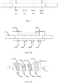
- heights of the four pins are generally designed to be the same, that is, the four pins are in one plane, as shown in FIG. 1 .
- the four pins are connected and the pins are prone to be electrolytically corroded during charging.
- electrolytic corrosion is avoided generally by increasing spacing between the four terminals.
- a size of a terminal component structure is increased, an integration level is relatively low, and a requirement for miniaturizing electronic products cannot be satisfied.
- the present invention provides a connector and a communications terminal, so as to resolve a prior-art problem of electrolytic corrosion in a connector while maintaining an integration level of the connector.
- a first aspect of embodiments of the present invention provides a connector, where the connector includes:
- the enclosure is further provided with a first protrusion and a second protrusion, where the first positioning hole is made into the first protrusion, the second positioning hole is made into the second protrusion, and a protrusion direction of the first protrusion is the same as a protrusion direction of the second protrusion;
- the first protrusion is located at an input end of the volt current condenser terminal on the enclosure, and the second protrusion is located at an input end of the ground terminal on the enclosure;
- the hole depth of the first positioning hole is greater than the hole depth of the third positioning hole, the hole depth of the first positioning hole is greater than the hole depth of the fourth positioning hole, the hole depth of the second positioning hole is greater than the hole depth of the third positioning hole, and the hole depth of the second positioning hole is greater than the hole depth of the fourth positioning hole;
- the length of the volt current condenser terminal is greater than the length of the D+ data transmission terminal and the length of the
- the enclosure is further provided with a third protrusion and a fourth protrusion, where the third positioning hole is made into the third protrusion, the fourth positioning hole is made into the fourth protrusion, and a protrusion direction of the third protrusion is the same as a protrusion direction of the fourth protrusion;
- the third protrusion is located at an input end of the D+ data transmission terminal on the enclosure, and the fourth protrusion is located at an input end of the D- data transmission terminal on the enclosure;
- the hole depth of the third positioning hole is greater than the hole depth of the first positioning hole, the hole depth of the third positioning hole is greater than the hole depth of the second positioning hole, the hole depth of the fourth positioning hole is greater than the hole depth of the first positioning hole, and the hole depth of the fourth positioning hole is greater than the hole depth of the second positioning hole;
- the length of the volt current condenser terminal is less than the length of the D+ data transmission terminal, the length of the
- a difference between the length of the volt current condenser terminal and the length of the D+ data transmission terminal ranges from 0.1 mm to 1.5 mm, or a difference between the length of the volt current condenser terminal and the length of the D- data transmission terminal ranges from 0.1 mm to 1.5 mm; and a difference between the hole depth of the first positioning hole and the hole depth of the third positioning hole ranges from 0.1 mm to 1.5 mm, and a difference between the hole depth of the first positioning hole and the hole depth of the fourth positioning hole ranges from 0.1 mm to 1.5 mm.
- a difference between the length of the ground terminal and the length of the D+ data transmission terminal ranges from 0.1 mm to 1.5 mm, or a difference between the length of the ground terminal and the length of the D- data transmission terminal ranges from 0.1 mm to 1.5 mm; and a difference between the hole depth of the second positioning hole and the hole depth of the third positioning hole ranges from 0.1 mm to 1.5 mm, and a difference between the hole depth of the second positioning hole and the hole depth of the fourth positioning hole ranges from 0.1 mm to 1.5 mm.
- a non-metallic material is attached to all of an outer peripheral wall of a pin shaft tail end, extending outwardly from the enclosure, of the volt current condenser terminal, an outer peripheral wall of a pin shaft tail end, extending outwardly from the enclosure, of the ground terminal, an outer peripheral wall of a pin shaft tail end, extending outwardly from the enclosure, of the D+ data transmission terminal, and an outer peripheral wall of a pin shaft tail end, extending outwardly from the enclosure, of the D- data transmission terminal.
- a second aspect of the present invention provides a communications terminal, where the communications terminal includes the connector according to any one of the first aspect or the first to the sixth implementation manners of the first aspect.
- a length of each terminal of the connector is modified, so that at least one of a volt current condenser terminal or a ground terminal is staggered from a D+ data transmission terminal and a D- data transmission terminal.
- the module division herein is merely logical division and may be other division in actual implementation. For example, a plurality of modules may be combined or integrated into another system, or some features may be ignored or not performed.
- the displayed or discussed mutual couplings or direct couplings or communication connections may be implemented by using some interfaces. Indirect couplings or communication connections between the modules may be implemented in electronic or other forms. No limitation is imposed herein.
- the modules or sub-modules described as separate parts may or may not be physically separate, may or may not be physical modules, or may not be distributed on a plurality of circuit modules. Some or all of the modules may be selected according to actual needs to achieve the objectives of the solutions of the embodiments of the present invention.
- the embodiments of the present invention provide a connector and a communications terminal for resolving a problem of electrolytic corrosion.
- the connector is mainly used for electronic products (for example, wearable devices such as Google glasses, sports bracelets, smart watches, or headsets), and may also be used for connector cables (at least one end of a connector cable may include the connector).
- a quantity of connectors on an electronic product, an arrangement of terminals on the connector, and a quantity of the terminals on the connector are not specifically limited herein.
- a connector is basically of a flat bottom
- a loop that is, an electrolytic environment
- a loop is prone to form between a volt current condenser terminal and a ground terminal, or between a volt current condenser terminal and a D+ data transmission terminal, or between a volt current condenser terminal and a D- data transmission terminal, or between a ground terminal and a D+ data transmission terminal, or between a ground terminal and a D- data transmission terminal.
- This will cause electrolytic corrosion, affecting a charging or signal transmission function.
- a loop formed between the D+ data transmission terminal and the D- data transmission terminal also does not affect the charging and signal transmission functions.
- the volt current condenser terminal, the data terminals, and the ground terminal on the connector are separated by means of staggered arrangement to avoid electrolytic corrosion even when there is a conductive liquid on the connector of the electronic product.
- the connector 1 includes:
- the enclosure 15 is provided with a first positioning hole 151 for fastening the volt current condenser terminal 11, a second positioning hole 152 for fastening the ground terminal 12, a third positioning hole 153 for fastening the D+ data transmission terminal 13, and a fourth positioning hole 154 for fastening the D- data transmission terminal 14.
- these terminals may be fastened on and connected to the enclosure 15 by means of assembly or in-mold injection.
- At least one of a hole depth of the first positioning hole 151 or a hole depth of the second positioning hole 152 is different from a hole depth of the third positioning hole 153 and is different from a hole depth of the fourth positioning hole 154.
- At least one of a length of the volt current condenser terminal 11 and a length of the ground terminal 12 is different from a length of the D+ data transmission terminal 13 and is different from a length of the D- data transmission terminal 14.
- the hole depth of the first positioning hole 151 is set corresponding to the length of the volt current condenser terminal 11, and the hole depth of the second positioning hole 152 is set corresponding to the length of the ground terminal 12.
- the volt current condenser terminal 11 is a solid terminal or a spring pin
- the ground terminal 12 is a solid terminal or a spring pin
- a material of the enclosure 15 is a non-metal material.
- a length of each terminal of the connector is modified, so that at least one of the volt current condenser terminal 11 or the ground terminal 12 is staggered from the D+ data transmission terminal 13 and the D- data transmission terminal 14, and at least one of the first positioning hole 151 or the second positioning hole 152 is staggered from the third positioning hole 153, to form a height difference or a step and avoid forming an electrolytic environment.
- This appropriate modification based on an actual product structure and shape can avoid electrolytic corrosion and effectively improve an integration level of electronic products without increasing considerable costs, so as to meet a current requirement for miniaturizing the electronic products.
- only the volt current condenser terminal 11 may be modified, or only the ground terminal 12 may be modified, or both the volt current condenser terminal 11 and the ground terminal 12 are modified, or only the D+ data transmission terminal 13 is modified, or only the D- data transmission terminal 14 is modified, or both the D+ data transmission terminal 13 and the D- data transmission terminal 14 are modified.
- a terminal is modified, an added length of the terminal is set corresponding to a depth of a positioning hole corresponding to the terminal.
- lengths of the two terminals may be the same or different, specifically depending on a product structure and shape. No limitation is imposed herein.
- the first protrusion 155 is located at an input end of the volt current condenser terminal 11 on the enclosure 15, and the second protrusion 156 is located at an input end of the ground terminal 12 on the enclosure 15.
- the input end refers to an end, on the volt current condenser terminal 11, that is in contact with the volt current condenser terminal 11 when an external signal is input to the volt current condenser terminal 11.
- Input ends of other terminals are similar to the input end of the volt current condenser terminal 11.
- the hole depth of the first positioning hole 151 is greater than the hole depth of the third positioning hole 153
- the hole depth of the first positioning hole 151 is greater than the hole depth of the fourth positioning hole 154
- the hole depth of the second positioning hole 152 is greater than the hole depth of the third positioning hole 153
- the hole depth of the second positioning hole 152 is greater than the hole depth of the fourth positioning hole 154.
- the length of the volt current condenser terminal 11 is greater than the length of the D+ data transmission terminal 13, and the length of the volt current condenser terminal 11 is greater than the length of the D- data transmission terminal 14.
- a length of the first positioning hole 151 that extends outwardly from the enclosure 15 is set corresponding to the length of the volt current condenser terminal 11.
- a length of the second positioning hole 152 that extends outwardly from the enclosure 15 is set corresponding to the length of the ground terminal 12.
- the first positioning hole 151 is staggered from the third positioning hole 153
- the first positioning hole 151 is staggered from the fourth positioning hole 154
- the second positioning hole 152 is staggered from the third positioning hole 153
- the second positioning hole 152 is staggered from the fourth positioning hole 154, so that a height difference is formed between their respective terminals, to avoid forming an electrolytic environment.
- the third protrusion 157 is located at an input end of the D+ data transmission terminal 13 on the enclosure, and the fourth protrusion 158 is located at an input end of the D- data transmission terminal 14 on the enclosure.
- the hole depth of the third positioning hole 153 is greater than the hole depth of the first positioning hole 151
- the hole depth of the third positioning hole 153 is greater than the hole depth of the second positioning hole 152
- the hole depth of the fourth positioning hole 154 is greater than the hole depth of the first positioning hole 151
- the hole depth of the fourth positioning hole 154 is greater than the hole depth of the second positioning hole 152.
- the length of the volt current condenser terminal 11 is less than the length of the D+ data transmission terminal 13, the length of the volt current condenser terminal 11 is less than the length of the D- data transmission terminal 14, the length of the ground terminal 12 is less than the length of the D+ data transmission terminal 13, and the length of the ground terminal 12 is less than the length of the D- data transmission terminal 14.
- a length of the third positioning hole 153 that extends outwardly from the enclosure 15 is set corresponding to the length of the D+ data transmission terminal 13.
- a length of the fourth positioning hole 154 that extends outwardly from the enclosure 15 is set corresponding to the length of the D- data transmission terminal 14.
- the third positioning hole 153 is staggered from the first positioning hole 151
- the third positioning hole 153 is staggered from the second positioning hole 152
- the fourth positioning hole 154 is staggered from the first positioning hole 151
- the fourth positioning hole 154 is staggered from the second positioning hole 152, so that a height difference is formed between their respective terminals, to avoid forming an electrolytic environment.
- the foregoing types of terminals can be effectively separated by simply modifying the related terminals and/or the enclosure, without needing to disassemble the connector into a plurality of components.
- the product shape does not need to be changed, costs are not increased, and an integration level of electronic products can be effectively increased, so as to meet a current requirement for miniaturizing the electronic products.
- the four terminals may also be separated by using a non-metallic material, to avoid electrolytic corrosion. Details are described as follows:
- Portions, connected to the enclosure 15, of the volt current condenser terminal 11, the ground terminal 12, the D+ data transmission terminal 13, and the D- data transmission terminal 14 are covered by a non-metallic material.
- the portions may be covered completely or partially, provided that a separation effect is achieved.
- a bottom of a pin shaft tail end of each terminal does not need to be covered by the non-metallic material.
- a non-metallic material is attached to an outer peripheral wall of a pin shaft tail end, extending outwardly from the enclosure 15, of the volt current condenser terminal 11, an outer peripheral wall of a pin shaft tail end, extending outwardly from the enclosure 15, of the ground terminal 12, an outer peripheral wall of a pin shaft tail end, extending outwardly from the enclosure 15, of the D+ data transmission terminal 13, and an outer peripheral wall of a pin shaft tail end, extending outwardly from the enclosure 15, the D- data transmission terminal 14.
- a same length may be increased for the volt current condenser terminal 11 and the ground terminal 12 to meet a product aesthetic demand; when the actual product structure or shape is changed, different lengths may be increased for the volt current condenser terminal 11 and the ground terminal 12, and a length of each terminal is set corresponding to a hole depth of a positioning hole, that is, an added length is the same as an added hole depth.
- a relationship between the length of the volt current condenser terminal 11, the depths of the first to fourth positioning holes, the length of the ground terminal 12, the length of the D+ data transmission terminal 13, or the length of the D- data transmission terminal 14 includes at least one of the following.
- a difference between the hole depth of the second positioning hole 152 and the hole depth of the third positioning hole 153 ranges from 0.1 mm to 1.5 mm, and a difference between the hole depth of the second positioning 152 hole and the hole depth of the fourth positioning hole 154 ranges from 0.1 mm to 1.5 mm.
- the communications terminal 2 includes the connector 1 described in any one of FIG. 2-1 to FIG. 3-5 .
- FIG. 4-2 is a rear view of a smart watch. In the figure, only that a volt current condenser terminal and a ground terminal are modified is used as an example. Other structures are similar. A specific structure is determined based on actual product design.
- the disclosed system, apparatus, and method may be implemented in other manners.
- the described apparatus embodiment is merely an example.
- the unit division is merely logical function division and may be other division in actual implementation.
- a plurality of units or components may be combined or integrated into another system, or some features may be ignored or not performed.
- the displayed or discussed mutual couplings or direct couplings or communication connections may be implemented by using some interfaces.
- the indirect couplings or communication connections between the apparatuses or units may be implemented in electronic, mechanical, or other forms.
- the units described as separate parts may or may not be physically separate, and parts displayed as units may or may not be physical units, may be located in one position, or may be distributed on a plurality of network units. Some or all of the units may be selected according to actual needs to achieve the objectives of the solutions of the embodiments.
- functional units in the embodiments of the present invention may be integrated into one processing unit, or each of the units may exist alone physically, or two or more units are integrated into one unit.
- the integrated unit may be implemented in a form of hardware, or may be implemented in a form of a software functional unit.
- the integrated unit When the integrated unit is implemented in the form of a software functional unit and sold or used as an independent product, the integrated unit may be stored in a computer-readable storage medium. Based on such an understanding, the technical solutions of the present invention essentially, or the part contributing to the prior art, or all or some of the technical solutions may be implemented in the form of a software product.
- the software product is stored in a storage medium and includes several instructions for instructing a computer device (which may be a personal computer, a server, or a network device) to perform all or some of the steps of the methods described in the embodiments of the present invention.
- the foregoing storage medium includes: any medium that can store program code, such as a USB flash drive, a removable hard disk, a read-only memory (ROM, Read-Only Memory), a random access memory (RAM, Random Access Memory), a magnetic disk, or an optical disc.
- program code such as a USB flash drive, a removable hard disk, a read-only memory (ROM, Read-Only Memory), a random access memory (RAM, Random Access Memory), a magnetic disk, or an optical disc.
Landscapes
- Chemical & Material Sciences (AREA)
- Engineering & Computer Science (AREA)
- Materials Engineering (AREA)
- Mechanical Engineering (AREA)
- Metallurgy (AREA)
- Organic Chemistry (AREA)
- Power Engineering (AREA)
- Physics & Mathematics (AREA)
- General Physics & Mathematics (AREA)
- Connector Housings Or Holding Contact Members (AREA)
- Details Of Connecting Devices For Male And Female Coupling (AREA)
Abstract
Description
- The present invention relates to the field of communications technologies, and in particular, to a connector and a communications terminal.
- At present, electronic products are generally provided with connectors, such as a charge terminal and a Universal Serial Bus (Universal Serial Bus, USB), for charging and signal transmission of the electronic products. The charge terminal is commonly used in a scenario in which a standard USB cannot be used, to implement charging and signal transmission in place of the USB. A most common charge terminal has four pins, can implement both charging and signal transmission, and usually has four terminals: a volt current condenser (Volt Current Condenser, VCC) terminal, a data positive (DATA+) terminal, a data negative (DATA-), and a ground (Ground, GND) terminal. When there is water, sweat, or another conductive liquid between the VCC terminal and the other three terminals, the VCC terminal is electrolytically corroded during charging, or when there is water, sweat, or another conductive liquid between the DATA+ and GND terminals and/or between the DATA- and GND terminals, the DATA+ terminal and the DATA- terminal are electrolytically corroded during charging. In this case, an appearance and charging performance of a product are affected, and even the product may not be used any more due to serious corrosion. Such an electrolytic corrosion phenomenon is common in electronic products, particularly in wearable products (such as a headset, a sports bracelet, an electronic wristwatch, and the like products that are worn for a long time). Sizes of pins, spacing between the pins, and the like of an existing charge terminal are different. For example, heights of the four pins are generally designed to be the same, that is, the four pins are in one plane, as shown in
FIG. 1 . When there is a small amount of water, sweat, or another conductive liquid on a surface of the charge terminal, the four pins are connected and the pins are prone to be electrolytically corroded during charging. - At present, electrolytic corrosion is avoided generally by increasing spacing between the four terminals. However, a size of a terminal component structure is increased, an integration level is relatively low, and a requirement for miniaturizing electronic products cannot be satisfied.
- The present invention provides a connector and a communications terminal, so as to resolve a prior-art problem of electrolytic corrosion in a connector while maintaining an integration level of the connector.
- A first aspect of embodiments of the present invention provides a connector, where the connector includes:
- a volt current condenser terminal, a ground terminal, a D+ data transmission terminal, a D- data transmission terminal, and an enclosure, where
- the enclosure is provided with a first positioning hole for fastening the volt current condenser terminal, a second positioning hole for fastening the ground terminal, a third positioning hole for fastening the D+ data transmission terminal, and a fourth positioning hole for fastening the D- data transmission terminal;
- at least one of a hole depth of the first positioning hole or a hole depth of the second positioning hole is different from a hole depth of the third positioning hole and is different from a hole depth of the fourth positioning hole;
- at least one of a length of the volt current condenser terminal or a length of the ground terminal is different from a length of the D+ data transmission terminal and is different from a length of the D- data transmission terminal; and
- the hole depth of the first positioning hole is set corresponding to the length of the volt current condenser terminal, and the hole depth of the second positioning hole is set corresponding to the length of the ground terminal.
- With reference to the first aspect, in a first implementation manner of the first aspect of the present invention, the enclosure is further provided with a first protrusion and a second protrusion, where the first positioning hole is made into the first protrusion, the second positioning hole is made into the second protrusion, and a protrusion direction of the first protrusion is the same as a protrusion direction of the second protrusion;
the first protrusion is located at an input end of the volt current condenser terminal on the enclosure, and the second protrusion is located at an input end of the ground terminal on the enclosure;
the hole depth of the first positioning hole is greater than the hole depth of the third positioning hole, the hole depth of the first positioning hole is greater than the hole depth of the fourth positioning hole, the hole depth of the second positioning hole is greater than the hole depth of the third positioning hole, and the hole depth of the second positioning hole is greater than the hole depth of the fourth positioning hole; and
the length of the volt current condenser terminal is greater than the length of the D+ data transmission terminal and the length of the D- data transmission terminal. - With reference to the first aspect, in a second implementation manner of the first aspect of the present invention, the enclosure is further provided with a third protrusion and a fourth protrusion, where the third positioning hole is made into the third protrusion, the fourth positioning hole is made into the fourth protrusion, and a protrusion direction of the third protrusion is the same as a protrusion direction of the fourth protrusion;
the third protrusion is located at an input end of the D+ data transmission terminal on the enclosure, and the fourth protrusion is located at an input end of the D- data transmission terminal on the enclosure;
the hole depth of the third positioning hole is greater than the hole depth of the first positioning hole, the hole depth of the third positioning hole is greater than the hole depth of the second positioning hole, the hole depth of the fourth positioning hole is greater than the hole depth of the first positioning hole, and the hole depth of the fourth positioning hole is greater than the hole depth of the second positioning hole; and
the length of the volt current condenser terminal is less than the length of the D+ data transmission terminal, the length of the volt current condenser terminal is less than the length of the D- data transmission terminal, the length of the ground terminal is less than the length of the D+ data transmission terminal, and the length of the ground terminal is less than the length of the D- data transmission terminal. - With reference to the first aspect or the first or the second implementation manner of the first aspect, in a third implementation manner of the first aspect of the present invention, a difference between the length of the volt current condenser terminal and the length of the D+ data transmission terminal ranges from 0.1 mm to 1.5 mm, or a difference between the length of the volt current condenser terminal and the length of the D- data transmission terminal ranges from 0.1 mm to 1.5 mm; and
a difference between the hole depth of the first positioning hole and the hole depth of the third positioning hole ranges from 0.1 mm to 1.5 mm, and a difference between the hole depth of the first positioning hole and the hole depth of the fourth positioning hole ranges from 0.1 mm to 1.5 mm. - With reference to any one of the first aspect or the first to the third implementation manners of the first aspect, in a fourth implementation manner of the first aspect of the present invention, a difference between the length of the ground terminal and the length of the D+ data transmission terminal ranges from 0.1 mm to 1.5 mm, or a difference between the length of the ground terminal and the length of the D- data transmission terminal ranges from 0.1 mm to 1.5 mm; and
a difference between the hole depth of the second positioning hole and the hole depth of the third positioning hole ranges from 0.1 mm to 1.5 mm, and a difference between the hole depth of the second positioning hole and the hole depth of the fourth positioning hole ranges from 0.1 mm to 1.5 mm. - With reference to any one of the first aspect or the first to the fourth implementation manners of the first aspect, in a fifth implementation manner of the first aspect of the present invention, a non-metallic material is attached to all of an outer peripheral wall of a pin shaft tail end, extending outwardly from the enclosure, of the volt current condenser terminal, an outer peripheral wall of a pin shaft tail end, extending outwardly from the enclosure, of the ground terminal, an outer peripheral wall of a pin shaft tail end, extending outwardly from the enclosure, of the D+ data transmission terminal, and an outer peripheral wall of a pin shaft tail end, extending outwardly from the enclosure, of the D- data transmission terminal.
- A second aspect of the present invention provides a communications terminal, where the communications terminal includes the connector according to any one of the first aspect or the first to the sixth implementation manners of the first aspect.
- In the embodiments of the present invention, a length of each terminal of the connector is modified, so that at least one of a volt current condenser terminal or a ground terminal is staggered from a D+ data transmission terminal and a D- data transmission terminal. This appropriate modification based on an actual product structure and shape can avoid electrolytic corrosion and effectively improve an integration level of electronic products without increasing considerable costs, so as to meet a current requirement for miniaturizing the electronic products.
-
-
FIG. 1 is a structural diagram of a connector in the prior art; -
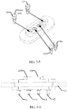
FIG. 2-1 is a side view of a connector according to an embodiment of the present invention; -
FIG. 2-2 is a side sectional view of a connector according to an embodiment of the present invention; -
FIG. 2-3 is a top view of an enclosure according to an embodiment of the present invention; -
FIG. 2-4 is a side view of an enclosure according to an embodiment of the present invention; -
FIG. 2-5 is an assembly view of a connector according to an embodiment of the present invention; -
FIG. 3-1 is a side view of another connector according to an embodiment of the present invention; -
FIG. 3-2 is a side sectional view of another connector according to an embodiment of the present invention; -
FIG. 3-3 is another top view of an enclosure according to an embodiment of the present invention; -
FIG. 3-4 is another side view of an enclosure according to an embodiment of the present invention; -
FIG. 3-5 is another assembly view of a connector according to an embodiment of the present invention; -
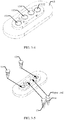
FIG. 4-1 is a structural diagram of a communications terminal according to an embodiment of the present invention; and -
FIG. 4-2 is a structural diagram of another communications terminal according to an embodiment of the present invention. - The following clearly and completely describes the technical solutions in the embodiments of the present invention with reference to the accompanying drawings in the embodiments of the present invention. Apparently, the described embodiments are a part rather than all of the embodiments of the present invention. All other embodiments obtained by a person of ordinary skill in the art based on the embodiments of the present invention without creative efforts shall fall within the protection scope of the present invention.
- In the specification, claims, and accompanying drawings of the present invention, the terms "first", "second", and so on are intended to distinguish between similar objects but do not necessarily indicate a specific order or sequence. It should be understood that the data termed in such a way are interchangeable in proper circumstances so that the embodiments of the present invention described herein can be implemented in an order other than the order illustrated or described herein. In addition, the terms "include", "contain", and any variation thereof are intended to cover a non-exclusive inclusion, for example, a process, method, system, product, or device that includes a series of steps or modules is not necessarily limited to those steps or modules that are expressly listed, but may include other steps or modules not expressly listed or inherent to such a process, method, product, or device. The module division herein is merely logical division and may be other division in actual implementation. For example, a plurality of modules may be combined or integrated into another system, or some features may be ignored or not performed. In addition, the displayed or discussed mutual couplings or direct couplings or communication connections may be implemented by using some interfaces. Indirect couplings or communication connections between the modules may be implemented in electronic or other forms. No limitation is imposed herein. In addition, the modules or sub-modules described as separate parts may or may not be physically separate, may or may not be physical modules, or may not be distributed on a plurality of circuit modules. Some or all of the modules may be selected according to actual needs to achieve the objectives of the solutions of the embodiments of the present invention.
- The embodiments of the present invention provide a connector and a communications terminal for resolving a problem of electrolytic corrosion. The connector is mainly used for electronic products (for example, wearable devices such as Google glasses, sports bracelets, smart watches, or headsets), and may also be used for connector cables (at least one end of a connector cable may include the connector). A quantity of connectors on an electronic product, an arrangement of terminals on the connector, and a quantity of the terminals on the connector are not specifically limited herein.
- In the prior art, because a connector is basically of a flat bottom, after there is a conductive liquid on a surface of the connector due to long-time wearing, a loop, that is, an electrolytic environment, is prone to form between a volt current condenser terminal and a ground terminal, or between a volt current condenser terminal and a D+ data transmission terminal, or between a volt current condenser terminal and a D- data transmission terminal, or between a ground terminal and a D+ data transmission terminal, or between a ground terminal and a D- data transmission terminal. This will cause electrolytic corrosion, affecting a charging or signal transmission function. In addition, a loop formed between the D+ data transmission terminal and the D- data transmission terminal also does not affect the charging and signal transmission functions.
- In the present invention, the volt current condenser terminal, the data terminals, and the ground terminal on the connector are separated by means of staggered arrangement to avoid electrolytic corrosion even when there is a conductive liquid on the connector of the electronic product.
- Referring to
FIG. 2-1 and FIG. 2-2 , a connector in an embodiment of the present invention is described, and theconnector 1 includes: - a volt
current condenser terminal 11, aground terminal 12, a D+data transmission terminal 13, a D-data transmission terminal 14, and anenclosure 15. - The
enclosure 15 is provided with afirst positioning hole 151 for fastening the voltcurrent condenser terminal 11, asecond positioning hole 152 for fastening theground terminal 12, athird positioning hole 153 for fastening the D+data transmission terminal 13, and afourth positioning hole 154 for fastening the D-data transmission terminal 14. In actual production, these terminals may be fastened on and connected to theenclosure 15 by means of assembly or in-mold injection. - At least one of a hole depth of the
first positioning hole 151 or a hole depth of thesecond positioning hole 152 is different from a hole depth of thethird positioning hole 153 and is different from a hole depth of thefourth positioning hole 154. - At least one of a length of the volt
current condenser terminal 11 and a length of theground terminal 12 is different from a length of the D+data transmission terminal 13 and is different from a length of the D-data transmission terminal 14. - The hole depth of the
first positioning hole 151 is set corresponding to the length of the voltcurrent condenser terminal 11, and the hole depth of thesecond positioning hole 152 is set corresponding to the length of theground terminal 12. - The volt
current condenser terminal 11 is a solid terminal or a spring pin, and theground terminal 12 is a solid terminal or a spring pin. A material of theenclosure 15 is a non-metal material. - In this embodiment of the present invention, a length of each terminal of the connector is modified, so that at least one of the volt
current condenser terminal 11 or theground terminal 12 is staggered from the D+data transmission terminal 13 and the D-data transmission terminal 14, and at least one of thefirst positioning hole 151 or thesecond positioning hole 152 is staggered from thethird positioning hole 153, to form a height difference or a step and avoid forming an electrolytic environment. This appropriate modification based on an actual product structure and shape can avoid electrolytic corrosion and effectively improve an integration level of electronic products without increasing considerable costs, so as to meet a current requirement for miniaturizing the electronic products. - Optionally, in some embodiments of the present invention, only the volt
current condenser terminal 11 may be modified, or only theground terminal 12 may be modified, or both the voltcurrent condenser terminal 11 and theground terminal 12 are modified, or only the D+data transmission terminal 13 is modified, or only the D-data transmission terminal 14 is modified, or both the D+data transmission terminal 13 and the D-data transmission terminal 14 are modified. When a terminal is modified, an added length of the terminal is set corresponding to a depth of a positioning hole corresponding to the terminal. In addition, when two terminals are modified, lengths of the two terminals may be the same or different, specifically depending on a product structure and shape. No limitation is imposed herein. - In this embodiment, how a problem of electrolytic corrosion is avoided is described by using examples in which both the volt
current condenser terminal 11 and theground terminal 12 are modified and both the D+data transmission terminal 13 and the D-data transmission terminal 14 are modified are used as examples. Other cases are similar and are not repeated herein. Details are described as follows: - I. Referring to
FIG. 2-1 toFIG. 2-4 , the voltcurrent condenser terminal 11 and theground terminal 12 may be modified as follows:- The
enclosure 15 is further provided with afirst protrusion 155 and asecond protrusion 156, thefirst positioning hole 151 is made into thefirst protrusion 155, thesecond positioning hole 152 is made into thesecond protrusion 156, and a protrusion direction of thefirst protrusion 155 is the same as a protrusion direction of thesecond protrusion 156.
- The
- The
first protrusion 155 is located at an input end of the voltcurrent condenser terminal 11 on theenclosure 15, and thesecond protrusion 156 is located at an input end of theground terminal 12 on theenclosure 15. The input end refers to an end, on the voltcurrent condenser terminal 11, that is in contact with the voltcurrent condenser terminal 11 when an external signal is input to the voltcurrent condenser terminal 11. Input ends of other terminals are similar to the input end of the voltcurrent condenser terminal 11. - The hole depth of the
first positioning hole 151 is greater than the hole depth of thethird positioning hole 153, the hole depth of thefirst positioning hole 151 is greater than the hole depth of thefourth positioning hole 154, the hole depth of thesecond positioning hole 152 is greater than the hole depth of thethird positioning hole 153, and the hole depth of thesecond positioning hole 152 is greater than the hole depth of thefourth positioning hole 154. - The length of the volt
current condenser terminal 11 is greater than the length of the D+data transmission terminal 13, and the length of the voltcurrent condenser terminal 11 is greater than the length of the D-data transmission terminal 14. - A length of the
first positioning hole 151 that extends outwardly from theenclosure 15 is set corresponding to the length of the voltcurrent condenser terminal 11. - A length of the
second positioning hole 152 that extends outwardly from theenclosure 15 is set corresponding to the length of theground terminal 12. - In this case, the
first positioning hole 151 is staggered from thethird positioning hole 153, thefirst positioning hole 151 is staggered from thefourth positioning hole 154, thesecond positioning hole 152 is staggered from thethird positioning hole 153, and thesecond positioning hole 152 is staggered from thefourth positioning hole 154, so that a height difference is formed between their respective terminals, to avoid forming an electrolytic environment. - II. Referring to
FIG. 3-1 toFIG. 3-5 , the D+data transmission terminal 13 and the D-data transmission terminal 14 may be modified as follows:- The
enclosure 15 is further provided with a third protrusion 157 and a fourth protrusion 158, thethird positioning hole 153 is made into the third protrusion 157, thefourth positioning hole 154 is made into thefourth protrusion 154, and a protrusion direction of the third protrusion 157 is the same as a protrusion direction of the fourth protrusion 158.
- The
- The third protrusion 157 is located at an input end of the D+
data transmission terminal 13 on the enclosure, and the fourth protrusion 158 is located at an input end of the D-data transmission terminal 14 on the enclosure. - The hole depth of the
third positioning hole 153 is greater than the hole depth of thefirst positioning hole 151, the hole depth of thethird positioning hole 153 is greater than the hole depth of thesecond positioning hole 152, the hole depth of thefourth positioning hole 154 is greater than the hole depth of thefirst positioning hole 151, and the hole depth of thefourth positioning hole 154 is greater than the hole depth of thesecond positioning hole 152. - The length of the volt
current condenser terminal 11 is less than the length of the D+data transmission terminal 13, the length of the voltcurrent condenser terminal 11 is less than the length of the D-data transmission terminal 14, the length of theground terminal 12 is less than the length of the D+data transmission terminal 13, and the length of theground terminal 12 is less than the length of the D-data transmission terminal 14. - A length of the
third positioning hole 153 that extends outwardly from theenclosure 15 is set corresponding to the length of the D+data transmission terminal 13. - A length of the
fourth positioning hole 154 that extends outwardly from theenclosure 15 is set corresponding to the length of the D-data transmission terminal 14. - In this case, the
third positioning hole 153 is staggered from thefirst positioning hole 151, thethird positioning hole 153 is staggered from thesecond positioning hole 152, thefourth positioning hole 154 is staggered from thefirst positioning hole 151, and thefourth positioning hole 154 is staggered from thesecond positioning hole 152, so that a height difference is formed between their respective terminals, to avoid forming an electrolytic environment. - According to the foregoing two solutions, the foregoing types of terminals can be effectively separated by simply modifying the related terminals and/or the enclosure, without needing to disassemble the connector into a plurality of components. Through the appropriate modification based on an actual product structure and shape, the product shape does not need to be changed, costs are not increased, and an integration level of electronic products can be effectively increased, so as to meet a current requirement for miniaturizing the electronic products.
- Optionally, in some embodiments of the present invention, on the basis of only modifying terminals without changing a structure of the
enclosure 15, the four terminals may also be separated by using a non-metallic material, to avoid electrolytic corrosion. Details are described as follows: - Portions, connected to the
enclosure 15, of the voltcurrent condenser terminal 11, theground terminal 12, the D+data transmission terminal 13, and the D-data transmission terminal 14 are covered by a non-metallic material. The portions may be covered completely or partially, provided that a separation effect is achieved. In addition, a bottom of a pin shaft tail end of each terminal does not need to be covered by the non-metallic material. - Optionally, a non-metallic material is attached to an outer peripheral wall of a pin shaft tail end, extending outwardly from the
enclosure 15, of the voltcurrent condenser terminal 11, an outer peripheral wall of a pin shaft tail end, extending outwardly from theenclosure 15, of theground terminal 12, an outer peripheral wall of a pin shaft tail end, extending outwardly from theenclosure 15, of the D+data transmission terminal 13, and an outer peripheral wall of a pin shaft tail end, extending outwardly from theenclosure 15, the D-data transmission terminal 14. - Optionally, when the volt
current condenser terminal 11 and theground terminal 12 are modified, or the D+data transmission terminal 13 and the D-data transmission terminal 14 are modified, a same length may be increased for the voltcurrent condenser terminal 11 and theground terminal 12 to meet a product aesthetic demand; when the actual product structure or shape is changed, different lengths may be increased for the voltcurrent condenser terminal 11 and theground terminal 12, and a length of each terminal is set corresponding to a hole depth of a positioning hole, that is, an added length is the same as an added hole depth. - A relationship between the length of the volt
current condenser terminal 11, the depths of the first to fourth positioning holes, the length of theground terminal 12, the length of the D+data transmission terminal 13, or the length of the D-data transmission terminal 14 includes at least one of the following. - 1. A difference between the length of the volt
current condenser terminal 11 and the length of the D+data transmission terminal 13 ranges from 0.1 mm to 1.5 mm, or a difference between the length of the voltcurrent condenser terminal 11 and the length of the D-data transmission terminal 14 ranges from 0.1 mm to 1.5 mm.
A difference between the hole depth of thefirst positioning hole 151 and the hole depth of thethird positioning hole 153 ranges from 0.1 mm to 1.5 mm, and a difference between the hole depth of thefirst positioning hole 151 and the hole depth of thefourth positioning hole 154 ranges from 0.1 mm to 1.5 mm. - 2. A difference between the length of the
ground terminal 12 and the length of the D+data transmission terminal 13 ranges from 0.1 mm to 1.5 mm, or a difference between the length of theground terminal 12 and the length of the D-data transmission terminal 14 ranges from 0.1 mm to 1.5 mm. - A difference between the hole depth of the
second positioning hole 152 and the hole depth of thethird positioning hole 153 ranges from 0.1 mm to 1.5 mm, and a difference between the hole depth of thesecond positioning 152 hole and the hole depth of thefourth positioning hole 154 ranges from 0.1 mm to 1.5 mm. - Referring to
FIG. 4-1 and FIG. 4-2 , a communications terminal in the present invention is described, and thecommunications terminal 2 includes theconnector 1 described in any one ofFIG. 2-1 toFIG. 3-5 . -
FIG. 4-2 is a rear view of a smart watch. In the figure, only that a volt current condenser terminal and a ground terminal are modified is used as an example. Other structures are similar. A specific structure is determined based on actual product design. - In the foregoing embodiments, the description of each embodiment has respective focuses. For a part that is not described in detail in an embodiment, reference may be made to related descriptions in other embodiments.
- It may be clearly understood by a person skilled in the art that, for the purpose of convenient and brief description, for a detailed working process of the foregoing system, apparatus, and unit, reference may be made to a corresponding process in the foregoing method embodiments, and details are not described herein again.
- In the several embodiments provided in this application, it should be understood that the disclosed system, apparatus, and method may be implemented in other manners. For example, the described apparatus embodiment is merely an example. For example, the unit division is merely logical function division and may be other division in actual implementation. For example, a plurality of units or components may be combined or integrated into another system, or some features may be ignored or not performed. In addition, the displayed or discussed mutual couplings or direct couplings or communication connections may be implemented by using some interfaces. The indirect couplings or communication connections between the apparatuses or units may be implemented in electronic, mechanical, or other forms.
- The units described as separate parts may or may not be physically separate, and parts displayed as units may or may not be physical units, may be located in one position, or may be distributed on a plurality of network units. Some or all of the units may be selected according to actual needs to achieve the objectives of the solutions of the embodiments.
- In addition, functional units in the embodiments of the present invention may be integrated into one processing unit, or each of the units may exist alone physically, or two or more units are integrated into one unit. The integrated unit may be implemented in a form of hardware, or may be implemented in a form of a software functional unit.
- When the integrated unit is implemented in the form of a software functional unit and sold or used as an independent product, the integrated unit may be stored in a computer-readable storage medium. Based on such an understanding, the technical solutions of the present invention essentially, or the part contributing to the prior art, or all or some of the technical solutions may be implemented in the form of a software product. The software product is stored in a storage medium and includes several instructions for instructing a computer device (which may be a personal computer, a server, or a network device) to perform all or some of the steps of the methods described in the embodiments of the present invention. The foregoing storage medium includes: any medium that can store program code, such as a USB flash drive, a removable hard disk, a read-only memory (ROM, Read-Only Memory), a random access memory (RAM, Random Access Memory), a magnetic disk, or an optical disc.
- The connector and the communications terminal provided in the present invention are described in detail above. The principle and implementation of the present invention are described herein through specific examples. The description about the foregoing embodiments is merely provided to help understand the method and core ideas of the present invention. In addition, a person of ordinary skill in the art can make variations and modifications to the present invention in terms of the specific implementations and application scopes according to the ideas of the present invention. Therefore, the content of specification shall not be construed as a limit to the present invention.
Claims (14)
- A connector, wherein the connector comprises:a volt current condenser terminal, a ground terminal, a D+ data transmission terminal, a D- data transmission terminal, and an enclosure, whereinthe enclosure is provided with a first positioning hole for fastening the volt current condenser terminal, a second positioning hole for fastening the ground terminal, a third positioning hole for fastening the D+ data transmission terminal, and a fourth positioning hole for fastening the D- data transmission terminal;at least one of a hole depth of the first positioning hole or a hole depth of the second positioning hole is different from a hole depth of the third positioning hole and is different from a hole depth of the fourth positioning hole;at least one of a length of the volt current condenser terminal or a length of the ground terminal is different from a length of the D+ data transmission terminal and is different from a length of the D- data transmission terminal; andthe hole depth of the first positioning hole is set corresponding to the length of the volt current condenser terminal, and the hole depth of the second positioning hole is set corresponding to the length of the ground terminal.
- The connector according to claim 1, wherein the enclosure is further provided with a first protrusion and a second protrusion, wherein the first positioning hole is made into the first protrusion, the second positioning hole is made into the second protrusion, and a protrusion direction of the first protrusion is the same as a protrusion direction of the second protrusion;
the first protrusion is located at an input end of the volt current condenser terminal on the enclosure, and the second protrusion is located at an input end of the ground terminal on the enclosure;
the hole depth of the first positioning hole is greater than the hole depth of the third positioning hole, the hole depth of the first positioning hole is greater than the hole depth of the fourth positioning hole, the hole depth of the second positioning hole is greater than the hole depth of the third positioning hole, and the hole depth of the second positioning hole is greater than the hole depth of the fourth positioning hole; and
the length of the volt current condenser terminal is greater than the length of the D+ data transmission terminal, and the length of the volt current condenser terminal is greater than the length of the D- data transmission terminal. - The connector according to claim 2, wherein a length of the first positioning hole that extends outwardly from the enclosure is set corresponding to the length of the volt current condenser terminal.
- The connector according to claim 2 or 3, wherein a length of the second positioning hole that extends outwardly from the enclosure is set corresponding to the length of the ground terminal.
- The connector according to claim 1, wherein the enclosure is further provided with a third protrusion and a fourth protrusion, wherein the third positioning hole is made into the third protrusion, the fourth positioning hole is made into the fourth protrusion, and a protrusion direction of the third protrusion is the same as a protrusion direction of the fourth protrusion;
the third protrusion is located at an input end of the D+ data transmission terminal on the enclosure, and the fourth protrusion is located at an input end of the D- data transmission terminal on the enclosure;
the hole depth of the third positioning hole is greater than the hole depth of the first positioning hole, the hole depth of the third positioning hole is greater than the hole depth of the second positioning hole, the hole depth of the fourth positioning hole is greater than the hole depth of the first positioning hole, and the hole depth of the fourth positioning hole is greater than the hole depth of the second positioning hole; and
the length of the volt current condenser terminal is less than the length of the D+ data transmission terminal and the length of the D- data transmission terminal, and the length of the ground terminal is less than the length of the D+ data transmission terminal and the length of the D- data transmission terminal length. - The connector according to claim 5, wherein a length of the third positioning hole that extends outwardly from the enclosure is set corresponding to the length of the D+ data transmission terminal.
- The connector according to claim 5 or 6, wherein
a length of the fourth positioning hole that extends outwardly from the enclosure is set corresponding to the length of the D- data transmission terminal. - The connector according to any one of claims 1 to 7, wherein a difference between the length of the volt current condenser terminal and the length of the D+ data transmission terminal ranges from 0.1 mm to 1.5 mm, or a difference between the length of the volt current condenser terminal and the length of the D- data transmission terminal ranges from 0.1 mm to 1.5 mm; and
a difference between the hole depth of the first positioning hole and the hole depth of the third positioning hole ranges from 0.1 mm to 1.5 mm, and a difference between the hole depth of the first positioning hole and the hole depth of the fourth positioning hole ranges from 0.1 mm to 1.5 mm. - The connector according to any one of claims 1 to 8, wherein a difference between the length of the ground terminal and the length of the D+ data transmission terminal ranges from 0.1 mm to 1.5 mm, or a difference between the length of the ground terminal and the length of the D- data transmission terminal ranges from 0.1 mm to 1.5 mm; and
a difference between the hole depth of the second positioning hole and the hole depth of the third positioning hole ranges from 0.1 mm to 1.5 mm, and a difference between the hole depth of the second positioning hole and the hole depth of the fourth positioning hole ranges from 0.1 mm to 1.5 mm. - The connector according to any one of claims 1 to 9, wherein a non-metallic material is attached to all of an outer peripheral wall of a pin shaft tail end, extending outwardly from the enclosure, of the volt current condenser terminal, an outer peripheral wall of a pin shaft tail end, extending outwardly from the enclosure, of the ground terminal, an outer peripheral wall of a pin shaft tail end, extending outwardly from the enclosure, of the D+ data transmission terminal, and an outer peripheral wall of a pin shaft tail end, extending outwardly from the enclosure, of the D- data transmission terminal.
- The connector according to any one of claims 1 to 10, wherein the volt current condenser terminal is a solid terminal or a spring pin, and
the ground terminal is a solid terminal or a spring pin. - The connecter according to any one of claims 1 to 11, wherein a material of the enclosure is a non-metallic material.
- The connector according to any one of claims 1 to 12, wherein the volt current condenser terminal, the ground terminal, the D+ data transmission terminal, and the D- data transmission terminal are fastened on and connected to the enclosure by means of assembly or in-mold injection.
- A communications terminal, wherein the communications terminal comprises the connector according to any one of claims 1 to 13.
Applications Claiming Priority (1)
| Application Number | Priority Date | Filing Date | Title |
|---|---|---|---|
| PCT/CN2015/090697 WO2017049581A1 (en) | 2015-09-25 | 2015-09-25 | Connector and communications device |
Publications (3)
| Publication Number | Publication Date |
|---|---|
| EP3300176A1 true EP3300176A1 (en) | 2018-03-28 |
| EP3300176A4 EP3300176A4 (en) | 2018-04-04 |
| EP3300176B1 EP3300176B1 (en) | 2020-08-12 |
Family
ID=58385717
Family Applications (1)
| Application Number | Title | Priority Date | Filing Date |
|---|---|---|---|
| EP15904457.7A Active EP3300176B1 (en) | 2015-09-25 | 2015-09-25 | Connector and communications device |
Country Status (6)
| Country | Link |
|---|---|
| US (1) | US10256562B2 (en) |
| EP (1) | EP3300176B1 (en) |
| JP (1) | JP6541282B2 (en) |
| KR (1) | KR102135657B1 (en) |
| CN (1) | CN106663893B (en) |
| WO (1) | WO2017049581A1 (en) |
Families Citing this family (3)
| Publication number | Priority date | Publication date | Assignee | Title |
|---|---|---|---|---|
| EP3936722B1 (en) * | 2020-07-06 | 2024-09-04 | Schott Ag | Housing part, especially housing part in particular for an electronic housing, preferably e-compressor terminal |
| USD1060265S1 (en) * | 2021-05-17 | 2025-02-04 | Schott Japan Corporation | Hermetic terminal |
| CN120917629A (en) * | 2023-12-29 | 2025-11-07 | 深圳市韶音科技有限公司 | Charging interface and wearable equipment |
Family Cites Families (16)
| Publication number | Priority date | Publication date | Assignee | Title |
|---|---|---|---|---|
| US3259870A (en) * | 1963-03-06 | 1966-07-05 | Albert & J M Anderson Mfg Co | Electrical connector |
| US3794957A (en) * | 1973-01-22 | 1974-02-26 | Anderson Power Products | Plural-poled, genderless electrical connector |
| JP2002134227A (en) | 2000-10-27 | 2002-05-10 | Sony Corp | Electrical connection device and electronic apparatus having the electrical connection device |
| JP4190015B2 (en) | 2005-11-02 | 2008-12-03 | 日本航空電子工業株式会社 | connector |
| JP2007207727A (en) | 2006-02-06 | 2007-08-16 | Yazaki Corp | Connector and connector mating structure |
| JP2008108675A (en) | 2006-10-27 | 2008-05-08 | Toshiba Corp | plug |
| JP5357563B2 (en) | 2009-02-16 | 2013-12-04 | ユニオンマシナリ株式会社 | High voltage multi-pole plug connector |
| US7833026B1 (en) | 2010-03-23 | 2010-11-16 | Tyco Electronics Corporation | Electrical connector system |
| JP5960383B2 (en) | 2010-06-01 | 2016-08-02 | スリーエム イノベイティブ プロパティズ カンパニー | Contact holder |
| US20120183262A1 (en) * | 2010-11-12 | 2012-07-19 | Research In Motion Limited | Connector for electrical and optical data circuits |
| CN102646882B (en) * | 2012-04-01 | 2014-01-29 | 东莞中探探针有限公司 | A USB2.0 connector socket and a plug used in conjunction with it |
| CN202930625U (en) * | 2012-11-08 | 2013-05-08 | 富港电子(东莞)有限公司 | Plug connector |
| JP5972800B2 (en) * | 2013-01-09 | 2016-08-17 | 株式会社ヨコオ | Electrical connector |
| TWM501006U (en) | 2015-03-02 | 2015-05-11 | Quanta Comp Inc | Electronic products and their wire sets |
| CN204538334U (en) | 2015-03-20 | 2015-08-05 | 东莞中探探针有限公司 | A waterproof switch connector |
| CN104868321B (en) | 2015-04-28 | 2018-10-12 | 昆山全方位电子科技有限公司 | A kind of electric connector |
-
2015
- 2015-09-25 CN CN201580025461.7A patent/CN106663893B/en active Active
- 2015-09-25 WO PCT/CN2015/090697 patent/WO2017049581A1/en not_active Ceased
- 2015-09-25 EP EP15904457.7A patent/EP3300176B1/en active Active
- 2015-09-25 KR KR1020187000366A patent/KR102135657B1/en not_active Expired - Fee Related
- 2015-09-25 US US15/738,998 patent/US10256562B2/en active Active
- 2015-09-25 JP JP2017565166A patent/JP6541282B2/en active Active
Also Published As
| Publication number | Publication date |
|---|---|
| JP6541282B2 (en) | 2019-07-10 |
| JP2018524773A (en) | 2018-08-30 |
| KR20180015246A (en) | 2018-02-12 |
| CN106663893A (en) | 2017-05-10 |
| US20180175533A1 (en) | 2018-06-21 |
| EP3300176A4 (en) | 2018-04-04 |
| EP3300176B1 (en) | 2020-08-12 |
| CN106663893B (en) | 2019-11-05 |
| KR102135657B1 (en) | 2020-07-20 |
| WO2017049581A1 (en) | 2017-03-30 |
| US10256562B2 (en) | 2019-04-09 |
Similar Documents
| Publication | Publication Date | Title |
|---|---|---|
| US9735522B2 (en) | Electrical receptacle connector | |
| CN206294254U (en) | Housing unit, dual camera module and mobile terminal | |
| JP3163905U (en) | High frequency micro connector | |
| TWM559006U (en) | Connector having signal terminals and ground terminals in different pitches and having ribs | |
| US8408940B2 (en) | Integrated connector | |
| CN104953279A (en) | Casing antenna and terminal | |
| CN109256647A (en) | Electric connector for socket | |
| US10256562B2 (en) | Connector and communications terminal | |
| US9484675B2 (en) | Terminal structure of electrical connector | |
| US20190356078A1 (en) | Cable connector assembly and manufacturing method thereof | |
| CN102769222A (en) | Connector socket structure | |
| US9640912B1 (en) | Bidirectional access portable flash drive | |
| US20160112781A1 (en) | Electronic device having maximum mounting space on circuit board | |
| US9705268B1 (en) | Connector with configuration pin between ground pin and power pin | |
| CN208045773U (en) | Ribbed connectors with signal and ground contacts at different pitches | |
| KR101374460B1 (en) | Usb connector having vertical to horizontal conversion contacts | |
| CN104377495A (en) | Socket electrical connector | |
| US9368922B2 (en) | Connector | |
| US9059549B2 (en) | Cable connector assembly having an improved cable with an equalizer function | |
| CN204315764U (en) | Electric connector for socket | |
| CN204991940U (en) | Body type antenna and terminal | |
| CN104505661B (en) | Socket connector | |
| CN206992378U (en) | A USB Type‑C connector | |
| CN205335569U (en) | Composite connector | |
| CN202121166U (en) | Connector plug with metal barrier to prevent crosstalk interference |
Legal Events
| Date | Code | Title | Description |
|---|---|---|---|
| STAA | Information on the status of an ep patent application or granted ep patent |
Free format text: STATUS: THE INTERNATIONAL PUBLICATION HAS BEEN MADE |
|
| PUAI | Public reference made under article 153(3) epc to a published international application that has entered the european phase |
Free format text: ORIGINAL CODE: 0009012 |
|
| STAA | Information on the status of an ep patent application or granted ep patent |
Free format text: STATUS: REQUEST FOR EXAMINATION WAS MADE |
|
| 17P | Request for examination filed |
Effective date: 20171221 |
|
| AK | Designated contracting states |
Kind code of ref document: A1 Designated state(s): AL AT BE BG CH CY CZ DE DK EE ES FI FR GB GR HR HU IE IS IT LI LT LU LV MC MK MT NL NO PL PT RO RS SE SI SK SM TR |
|
| AX | Request for extension of the european patent |
Extension state: BA ME |
|
| A4 | Supplementary search report drawn up and despatched |
Effective date: 20180306 |
|
| RIC1 | Information provided on ipc code assigned before grant |
Ipc: H01R 13/52 20060101ALN20180228BHEP Ipc: H01R 13/24 20060101AFI20180228BHEP Ipc: G04G 19/00 20060101ALI20180228BHEP Ipc: H01R 13/62 20060101ALN20180228BHEP Ipc: H01R 13/405 20060101ALI20180228BHEP |
|
| DAV | Request for validation of the european patent (deleted) | ||
| DAX | Request for extension of the european patent (deleted) | ||
| REG | Reference to a national code |
Ref country code: DE Ref legal event code: R079 Ref document number: 602015057553 Country of ref document: DE Free format text: PREVIOUS MAIN CLASS: H01R0013020000 Ipc: H01R0013240000 |
|
| GRAP | Despatch of communication of intention to grant a patent |
Free format text: ORIGINAL CODE: EPIDOSNIGR1 |
|
| STAA | Information on the status of an ep patent application or granted ep patent |
Free format text: STATUS: GRANT OF PATENT IS INTENDED |
|
| RIC1 | Information provided on ipc code assigned before grant |
Ipc: H01R 13/24 20060101AFI20200302BHEP Ipc: G04G 19/00 20060101ALI20200302BHEP Ipc: H01R 13/52 20060101ALN20200302BHEP Ipc: H01R 13/405 20060101ALI20200302BHEP Ipc: H01R 13/62 20060101ALN20200302BHEP |
|
| INTG | Intention to grant announced |
Effective date: 20200327 |
|
| GRAS | Grant fee paid |
Free format text: ORIGINAL CODE: EPIDOSNIGR3 |
|
| GRAA | (expected) grant |
Free format text: ORIGINAL CODE: 0009210 |
|
| STAA | Information on the status of an ep patent application or granted ep patent |
Free format text: STATUS: THE PATENT HAS BEEN GRANTED |
|
| AK | Designated contracting states |
Kind code of ref document: B1 Designated state(s): AL AT BE BG CH CY CZ DE DK EE ES FI FR GB GR HR HU IE IS IT LI LT LU LV MC MK MT NL NO PL PT RO RS SE SI SK SM TR |
|
| REG | Reference to a national code |
Ref country code: CH Ref legal event code: EP |
|
| REG | Reference to a national code |
Ref country code: DE Ref legal event code: R096 Ref document number: 602015057553 Country of ref document: DE |
|
| REG | Reference to a national code |
Ref country code: IE Ref legal event code: FG4D |
|
| REG | Reference to a national code |
Ref country code: AT Ref legal event code: REF Ref document number: 1302468 Country of ref document: AT Kind code of ref document: T Effective date: 20200915 |
|
| REG | Reference to a national code |
Ref country code: LT Ref legal event code: MG4D |
|
| REG | Reference to a national code |
Ref country code: NL Ref legal event code: MP Effective date: 20200812 |
|
| PG25 | Lapsed in a contracting state [announced via postgrant information from national office to epo] |
Ref country code: FI Free format text: LAPSE BECAUSE OF FAILURE TO SUBMIT A TRANSLATION OF THE DESCRIPTION OR TO PAY THE FEE WITHIN THE PRESCRIBED TIME-LIMIT Effective date: 20200812 Ref country code: BG Free format text: LAPSE BECAUSE OF FAILURE TO SUBMIT A TRANSLATION OF THE DESCRIPTION OR TO PAY THE FEE WITHIN THE PRESCRIBED TIME-LIMIT Effective date: 20201112 Ref country code: SE Free format text: LAPSE BECAUSE OF FAILURE TO SUBMIT A TRANSLATION OF THE DESCRIPTION OR TO PAY THE FEE WITHIN THE PRESCRIBED TIME-LIMIT Effective date: 20200812 Ref country code: GR Free format text: LAPSE BECAUSE OF FAILURE TO SUBMIT A TRANSLATION OF THE DESCRIPTION OR TO PAY THE FEE WITHIN THE PRESCRIBED TIME-LIMIT Effective date: 20201113 Ref country code: HR Free format text: LAPSE BECAUSE OF FAILURE TO SUBMIT A TRANSLATION OF THE DESCRIPTION OR TO PAY THE FEE WITHIN THE PRESCRIBED TIME-LIMIT Effective date: 20200812 Ref country code: NO Free format text: LAPSE BECAUSE OF FAILURE TO SUBMIT A TRANSLATION OF THE DESCRIPTION OR TO PAY THE FEE WITHIN THE PRESCRIBED TIME-LIMIT Effective date: 20201112 Ref country code: LT Free format text: LAPSE BECAUSE OF FAILURE TO SUBMIT A TRANSLATION OF THE DESCRIPTION OR TO PAY THE FEE WITHIN THE PRESCRIBED TIME-LIMIT Effective date: 20200812 |
|
| REG | Reference to a national code |
Ref country code: AT Ref legal event code: MK05 Ref document number: 1302468 Country of ref document: AT Kind code of ref document: T Effective date: 20200812 |
|
| PG25 | Lapsed in a contracting state [announced via postgrant information from national office to epo] |
Ref country code: PL Free format text: LAPSE BECAUSE OF FAILURE TO SUBMIT A TRANSLATION OF THE DESCRIPTION OR TO PAY THE FEE WITHIN THE PRESCRIBED TIME-LIMIT Effective date: 20200812 Ref country code: NL Free format text: LAPSE BECAUSE OF FAILURE TO SUBMIT A TRANSLATION OF THE DESCRIPTION OR TO PAY THE FEE WITHIN THE PRESCRIBED TIME-LIMIT Effective date: 20200812 Ref country code: LV Free format text: LAPSE BECAUSE OF FAILURE TO SUBMIT A TRANSLATION OF THE DESCRIPTION OR TO PAY THE FEE WITHIN THE PRESCRIBED TIME-LIMIT Effective date: 20200812 Ref country code: RS Free format text: LAPSE BECAUSE OF FAILURE TO SUBMIT A TRANSLATION OF THE DESCRIPTION OR TO PAY THE FEE WITHIN THE PRESCRIBED TIME-LIMIT Effective date: 20200812 Ref country code: IS Free format text: LAPSE BECAUSE OF FAILURE TO SUBMIT A TRANSLATION OF THE DESCRIPTION OR TO PAY THE FEE WITHIN THE PRESCRIBED TIME-LIMIT Effective date: 20201212 |
|
| PG25 | Lapsed in a contracting state [announced via postgrant information from national office to epo] |
Ref country code: EE Free format text: LAPSE BECAUSE OF FAILURE TO SUBMIT A TRANSLATION OF THE DESCRIPTION OR TO PAY THE FEE WITHIN THE PRESCRIBED TIME-LIMIT Effective date: 20200812 Ref country code: SM Free format text: LAPSE BECAUSE OF FAILURE TO SUBMIT A TRANSLATION OF THE DESCRIPTION OR TO PAY THE FEE WITHIN THE PRESCRIBED TIME-LIMIT Effective date: 20200812 Ref country code: RO Free format text: LAPSE BECAUSE OF FAILURE TO SUBMIT A TRANSLATION OF THE DESCRIPTION OR TO PAY THE FEE WITHIN THE PRESCRIBED TIME-LIMIT Effective date: 20200812 Ref country code: CZ Free format text: LAPSE BECAUSE OF FAILURE TO SUBMIT A TRANSLATION OF THE DESCRIPTION OR TO PAY THE FEE WITHIN THE PRESCRIBED TIME-LIMIT Effective date: 20200812 Ref country code: DK Free format text: LAPSE BECAUSE OF FAILURE TO SUBMIT A TRANSLATION OF THE DESCRIPTION OR TO PAY THE FEE WITHIN THE PRESCRIBED TIME-LIMIT Effective date: 20200812 |
|
| REG | Reference to a national code |
Ref country code: CH Ref legal event code: PL |
|
| REG | Reference to a national code |
Ref country code: DE Ref legal event code: R097 Ref document number: 602015057553 Country of ref document: DE |
|
| PG25 | Lapsed in a contracting state [announced via postgrant information from national office to epo] |
Ref country code: MC Free format text: LAPSE BECAUSE OF FAILURE TO SUBMIT A TRANSLATION OF THE DESCRIPTION OR TO PAY THE FEE WITHIN THE PRESCRIBED TIME-LIMIT Effective date: 20200812 Ref country code: AL Free format text: LAPSE BECAUSE OF FAILURE TO SUBMIT A TRANSLATION OF THE DESCRIPTION OR TO PAY THE FEE WITHIN THE PRESCRIBED TIME-LIMIT Effective date: 20200812 Ref country code: AT Free format text: LAPSE BECAUSE OF FAILURE TO SUBMIT A TRANSLATION OF THE DESCRIPTION OR TO PAY THE FEE WITHIN THE PRESCRIBED TIME-LIMIT Effective date: 20200812 Ref country code: ES Free format text: LAPSE BECAUSE OF FAILURE TO SUBMIT A TRANSLATION OF THE DESCRIPTION OR TO PAY THE FEE WITHIN THE PRESCRIBED TIME-LIMIT Effective date: 20200812 |
|
| PLBE | No opposition filed within time limit |
Free format text: ORIGINAL CODE: 0009261 |
|
| REG | Reference to a national code |
Ref country code: BE Ref legal event code: MM Effective date: 20200930 |
|
| STAA | Information on the status of an ep patent application or granted ep patent |
Free format text: STATUS: NO OPPOSITION FILED WITHIN TIME LIMIT |
|
| PG25 | Lapsed in a contracting state [announced via postgrant information from national office to epo] |
Ref country code: LU Free format text: LAPSE BECAUSE OF NON-PAYMENT OF DUE FEES Effective date: 20200925 Ref country code: SK Free format text: LAPSE BECAUSE OF FAILURE TO SUBMIT A TRANSLATION OF THE DESCRIPTION OR TO PAY THE FEE WITHIN THE PRESCRIBED TIME-LIMIT Effective date: 20200812 |
|
| 26N | No opposition filed |
Effective date: 20210514 |
|
| PG25 | Lapsed in a contracting state [announced via postgrant information from national office to epo] |
Ref country code: IT Free format text: LAPSE BECAUSE OF FAILURE TO SUBMIT A TRANSLATION OF THE DESCRIPTION OR TO PAY THE FEE WITHIN THE PRESCRIBED TIME-LIMIT Effective date: 20200812 |
|
| PG25 | Lapsed in a contracting state [announced via postgrant information from national office to epo] |
Ref country code: BE Free format text: LAPSE BECAUSE OF NON-PAYMENT OF DUE FEES Effective date: 20200930 Ref country code: CH Free format text: LAPSE BECAUSE OF NON-PAYMENT OF DUE FEES Effective date: 20200930 Ref country code: SI Free format text: LAPSE BECAUSE OF FAILURE TO SUBMIT A TRANSLATION OF THE DESCRIPTION OR TO PAY THE FEE WITHIN THE PRESCRIBED TIME-LIMIT Effective date: 20200812 Ref country code: IE Free format text: LAPSE BECAUSE OF NON-PAYMENT OF DUE FEES Effective date: 20200925 Ref country code: LI Free format text: LAPSE BECAUSE OF NON-PAYMENT OF DUE FEES Effective date: 20200930 |
|
| PG25 | Lapsed in a contracting state [announced via postgrant information from national office to epo] |
Ref country code: TR Free format text: LAPSE BECAUSE OF FAILURE TO SUBMIT A TRANSLATION OF THE DESCRIPTION OR TO PAY THE FEE WITHIN THE PRESCRIBED TIME-LIMIT Effective date: 20200812 Ref country code: MT Free format text: LAPSE BECAUSE OF FAILURE TO SUBMIT A TRANSLATION OF THE DESCRIPTION OR TO PAY THE FEE WITHIN THE PRESCRIBED TIME-LIMIT Effective date: 20200812 Ref country code: CY Free format text: LAPSE BECAUSE OF FAILURE TO SUBMIT A TRANSLATION OF THE DESCRIPTION OR TO PAY THE FEE WITHIN THE PRESCRIBED TIME-LIMIT Effective date: 20200812 |
|
| PG25 | Lapsed in a contracting state [announced via postgrant information from national office to epo] |
Ref country code: MK Free format text: LAPSE BECAUSE OF FAILURE TO SUBMIT A TRANSLATION OF THE DESCRIPTION OR TO PAY THE FEE WITHIN THE PRESCRIBED TIME-LIMIT Effective date: 20200812 |
|
| PG25 | Lapsed in a contracting state [announced via postgrant information from national office to epo] |
Ref country code: PT Free format text: LAPSE BECAUSE OF FAILURE TO SUBMIT A TRANSLATION OF THE DESCRIPTION OR TO PAY THE FEE WITHIN THE PRESCRIBED TIME-LIMIT Effective date: 20200812 |
|
| PGFP | Annual fee paid to national office [announced via postgrant information from national office to epo] |
Ref country code: DE Payment date: 20250730 Year of fee payment: 11 |
|
| PGFP | Annual fee paid to national office [announced via postgrant information from national office to epo] |
Ref country code: GB Payment date: 20250807 Year of fee payment: 11 |
|
| PGFP | Annual fee paid to national office [announced via postgrant information from national office to epo] |
Ref country code: FR Payment date: 20250808 Year of fee payment: 11 |