EP3300109A1 - Integrated circuit with protection from transient electrical stress events and method therefor - Google Patents
Integrated circuit with protection from transient electrical stress events and method therefor Download PDFInfo
- Publication number
- EP3300109A1 EP3300109A1 EP17188997.5A EP17188997A EP3300109A1 EP 3300109 A1 EP3300109 A1 EP 3300109A1 EP 17188997 A EP17188997 A EP 17188997A EP 3300109 A1 EP3300109 A1 EP 3300109A1
- Authority
- EP
- European Patent Office
- Prior art keywords
- coupled
- output signal
- supply voltage
- inverter
- circuit
- Prior art date
- Legal status (The legal status is an assumption and is not a legal conclusion. Google has not performed a legal analysis and makes no representation as to the accuracy of the status listed.)
- Granted
Links
Images


Classifications
-
- H—ELECTRICITY
- H03—ELECTRONIC CIRCUITRY
- H03K—PULSE TECHNIQUE
- H03K19/00—Logic circuits, i.e. having at least two inputs acting on one output; Inverting circuits
- H03K19/20—Logic circuits, i.e. having at least two inputs acting on one output; Inverting circuits characterised by logic function, e.g. AND, OR, NOR, NOT circuits
-
- H—ELECTRICITY
- H10—SEMICONDUCTOR DEVICES; ELECTRIC SOLID-STATE DEVICES NOT OTHERWISE PROVIDED FOR
- H10D—INORGANIC ELECTRIC SEMICONDUCTOR DEVICES
- H10D89/00—Aspects of integrated devices not covered by groups H10D84/00 - H10D88/00
- H10D89/60—Integrated devices comprising arrangements for electrical or thermal protection, e.g. protection circuits against electrostatic discharge [ESD]
-
- H—ELECTRICITY
- H02—GENERATION; CONVERSION OR DISTRIBUTION OF ELECTRIC POWER
- H02H—EMERGENCY PROTECTIVE CIRCUIT ARRANGEMENTS
- H02H9/00—Emergency protective circuit arrangements for limiting excess current or voltage without disconnection
- H02H9/04—Emergency protective circuit arrangements for limiting excess current or voltage without disconnection responsive to excess voltage
- H02H9/045—Emergency protective circuit arrangements for limiting excess current or voltage without disconnection responsive to excess voltage adapted to a particular application and not provided for elsewhere
- H02H9/046—Emergency protective circuit arrangements for limiting excess current or voltage without disconnection responsive to excess voltage adapted to a particular application and not provided for elsewhere responsive to excess voltage appearing at terminals of integrated circuits
-
- H—ELECTRICITY
- H10—SEMICONDUCTOR DEVICES; ELECTRIC SOLID-STATE DEVICES NOT OTHERWISE PROVIDED FOR
- H10D—INORGANIC ELECTRIC SEMICONDUCTOR DEVICES
- H10D89/00—Aspects of integrated devices not covered by groups H10D84/00 - H10D88/00
- H10D89/60—Integrated devices comprising arrangements for electrical or thermal protection, e.g. protection circuits against electrostatic discharge [ESD]
- H10D89/601—Integrated devices comprising arrangements for electrical or thermal protection, e.g. protection circuits against electrostatic discharge [ESD] for devices having insulated gate electrodes, e.g. for IGFETs or IGBTs
- H10D89/811—Integrated devices comprising arrangements for electrical or thermal protection, e.g. protection circuits against electrostatic discharge [ESD] for devices having insulated gate electrodes, e.g. for IGFETs or IGBTs using FETs as protective elements
- H10D89/819—Bias arrangements for gate electrodes of FETs, e.g. RC networks or voltage partitioning circuits
-
- H—ELECTRICITY
- H10—SEMICONDUCTOR DEVICES; ELECTRIC SOLID-STATE DEVICES NOT OTHERWISE PROVIDED FOR
- H10W—GENERIC PACKAGES, INTERCONNECTIONS, CONNECTORS OR OTHER CONSTRUCTIONAL DETAILS OF DEVICES COVERED BY CLASS H10
- H10W42/00—Arrangements for protection of devices
- H10W42/60—Arrangements for protection of devices protecting against electrostatic charges or discharges, e.g. Faraday shields
Definitions
- This disclosure relates generally to integrated circuits (ICs), and more specifically, to protection from transient electrical stress (TES) events for integrated circuits.
- ICs integrated circuits
- TES transient electrical stress
- Electronic circuits are designed to operate over limited voltage ranges. Exposure to voltages beyond those limited voltage ranges can damage or destroy those circuits. The problem is particularly notable for integrated circuits, which often have many external terminals connected to circuitry fabricated on a very small scale.
- Transient voltage suppression circuits for integrated circuits should function for both unpowered transient events (i.e., those transient events occurring when the integrated circuit is not powered up for normal operation) and powered transient events (i.e., those transient events occurring when power is applied to the integrated circuit for normal operation).
- Unpowered TES events may include, but are not limited to, Electrostatic Discharge events (ESD), for example Human Body Model (HBM), Machine Model, or Charged Device Model (CDM) events.
- Powered TES events may include, but are not limited to, Powered ESD (PESD), Electric Fast Transient (EFT), Power Surge, or Ring Wave events.
- an integrated circuit for protecting against transient electrical stress events comprising: a trigger circuit including: a first detection circuit coupled to a first supply voltage; a second detection circuit coupled to a second supply voltage; a rail clamp device, wherein during a first type of electrical stress event, the rail clamp device is activated in response to a first output signal provided by the first detection circuit, and during a second type of electrical stress event, the rail clamp device is activated in response to a second output signal provided by the second detection circuit.
- a transient electrical stress (TES) event refers to a fast rise in voltage at a net inside an electronic circuit which may result in damage or destruction of electronic circuits coupled to that net. Therefore, with TES event protection circuitry, a trigger circuit detects a transient voltage increase corresponding to a TES event, and, in response, places a clamping device into a conductive state to provide a current path to safely dissipate the associated stress current and to limit the transient voltage during the TES event.
- a large MOS device is often used as the clamping device between two supply rails, and the conductivity of the large MOS device is controlled by the trigger circuit. In many cases, an array of large MOS clamping devices is used with their gate terminals biased by a shared trigger circuit.
- the MOS clamping device does not reach its breakdown voltage as this may lead to the destruction of the clamping device and therefore cause permanent damage to the electronic circuit.
- the normal operating voltage and the breakdown voltage of the MOS clamping device are very close, thus the design margin for the trigger circuit activating before the MOS device goes into breakdown is very tight, limiting the ability of the MOS device to operate as a clamping device.
- a separate (boosted) supply is used for powering the trigger circuit. All external pads, including I/O and power supply pads, are coupled to this boosted supply via pull-up diodes, ensuring that the boosted supply carries the highest possible potential.
- the boosted supply is typically charged up to the voltage level of the main power supply. If a TES event occurs on an I/O pin, the voltage on the boosted supply is elevated above the main power supply, which carries most of the TES current and connects to the drain terminal of the clamping device. Therefore, the trigger circuit can provide a gate voltage to the clamping device higher than the voltage on its drain.
- Overdriving the gate of the clamping device increases its on-conductance and therefore its TES protection efficiency. This improves design margins for TES events which occur on an I/O pad, resulting in a greater margin between the peak stress voltage and the breakdown voltage of the clamping device or any other device coupled to the stressed I/O pad (for example, input or output buffers) or coupled to the main power supply.
- the supply voltage to the trigger circuit may be lower than the voltage across the clamping device, making the design margin of conventional boosted designs worse as compared to non-boosted designs.
- the overvoltage level on the main power supply needed to activate the trigger circuit via the boosted supply is higher as compared to non-boosted designs. This is because the boosted supply voltage is reduced by the pull-up diode from the main power supply.
- the resulting activation voltage for a TES event on the main power supply can be higher than the breakdown voltage of the clamping device, which may cause its destruction.
- a trigger circuit having multiple filters coupled to different supply voltages is used to activate the clamping device.
- the trigger circuit can be designed to activate when any of the different supply voltages experiences a fast rising voltage ramp without causing damage to the electronic circuit.
- the TES event protection circuitry described below functions for both powered and unpowered transient events.
- FIG. 1 illustrates an integrated circuit 10 having a boosted TES protection scheme.
- IC 10 includes a first power supply rail (VDD) 12, a first power supply pad 13 coupled to VDD 12, an I/O pad 14, a second power supply rail (VSS) 16, a second power supply pad 15 coupled to VSS 16, a boost bus 11, a trigger circuit 28, a clamping device 26, and diodes 18, 20, 22, and 24.
- first power supply rail 12 may be a positive supply rail and second power supply rail may be a negative supply rail or ground.
- Clamping device 26 may be an N-channel metal oxide semiconductor field effect transistor (MOSFET or MOS transistor).
- Boost bus 11 is coupled to trigger circuit 28 to provide a third power supply BOOST to trigger circuit 28.
- MOSFET metal oxide semiconductor field effect transistor
- Diode 22 has an anode coupled to VSS 16 and a cathode coupled to I/O pad 14, to an anode of diode 18.
- a cathode of diode 18 is coupled to boost bus 11.
- An anode of diode 20 is coupled to I/O pad 14, and a cathode of diode 20 is coupled to VDD 12.
- a first current electrode of clamping device 26 is coupled to VDD 12
- a second current electrode of clamping device 26 is coupled to VSS 16
- a control electrode of clamping device 26 is coupled to receive a signal, TRIGGER, from trigger circuit 28.
- Trigger circuit 28 is also coupled to VDD 12 and VSS 16.
- An anode of diode 24 is coupled to VDD 12 and a cathode of diode 24 is coupled to boost bus 11.
- circuits coupled to I/O pad 14 are protected by diodes, which shunt any TES current to VSS 16 or VDD 12, depending on the polarity of the TES event.
- Diode 22 conducts any TES current that leaves I/O pad 14.
- Diode 20 and clamping device 26 are the primary shunt path for TES current injected into I/O pad 14.
- trigger circuit 28 drives the control electrode of clamping device 26 to a voltage level needed for clamping device 26 to shunt the TES current between VDD 12 and VSS 16.
- a large TES current flows through VDD supply rail 12. Because of the resistive voltage drop in the VDD supply rail, the supply voltage will vary with position, i.e. it will decrease over distance to the stressed I/O pad.
- the supply voltage VDD will be highest at diode 20.
- boost bus 11 is powered from I/O pad 14 during a TES event that injects current into I/O pad 14.
- Diode 18 and boost bus 11 are designed to have a lower resistive voltage drop than diode 20 and VDD supply rail 12 so that boost bus 11 can provide a higher supply voltage, at node BOOST, to trigger circuit 28. This is mainly due to the fact that there is little current flowing through diode 18 and boost bus 11 as they are not part of the primary TES current dissipation path.
- clamping device 26 In this manner, a higher voltage is provided to the control electrode of clamping device 26 by the trigger circuit, allowing clamping device 26 to be made smaller to achieve a similar on-conductance compared to a non-boosted design where the trigger circuit would be powered directly by the VDD supply rail.
- a drawback of this topology is that when TES current is injected directly onto VDD 12, boost bus 11 is powered from VDD 12, through diode 24.
- the trigger circuit gets activated by a fast rising supply voltage that exceeds the activation voltage of the trigger circuit.
- the voltage drop in diode 24 reduces the supply voltage at node BOOST to trigger circuit 28 during a TES event.
- boost bus 11 is typically charged up to the voltage level of VDD 12. Therefore, the overvoltage on the VDD supply during a TES event needed to activate the trigger circuit though diode 24 is increased compared to a non-boosted design.
- trigger circuit 28 can effectively provide TES protection when a TES event occurs on either VDD 12 or I/O pad 14.
- FIG 2 illustrates in partial schematic and partial block diagram form, trigger circuit 28 of FIG. 1 .
- Trigger circuit 28 includes a resistor-capacitor (RC) timer 32, an RC timer 34, and a logic circuit 36.
- RC timer 32 is implemented as a filter 38
- RC timer 34 is implemented as a filter 40.
- RC timers 32 and 34 may also be referred to as TES detection circuits, and they get activated by a fast rising voltage supply with a rise time that is within the range of the R*C time constant of the RC timers.
- clamping device 26 is also illustrated in FIG. 2.
- Logic circuit 36 is coupled to BOOST (which may be coupled to boost bus 11) and VSS (which may be coupled to VSS 16).
- logic circuit 36 may also be coupled to VDD (which may be coupled to VDD 12) in addition to BOOST and VSS.
- Logic circuit 36 has a first input coupled to filter 40, a second input coupled to filter 38, and an output coupled to provide a trigger signal on the TRIGGER node to the control electrode of clamping device 26.
- Filter 38 is coupled to VDD and VSS and provides an output to the second input of logic circuit 36.
- Filter 40 is coupled to BOOST and VSS and provides an output to the first input of logic circuit 36.
- each filter 38 and 40 is coupled to a different voltage supply, VDD and BOOST, respectively. Therefore, the TRIGGER signal will be asserted to activate clamping device 26 when either supply experiences a fast rising voltage ramp above the activation voltage of the trigger circuit, due, for example, to a TES event.
- trigger circuit 28 can be used to improve triggering for TES events at I/O pad 14 (in which BOOST is higher than VDD) without negatively impacting the trigger circuit activation for TES events at VDD (in which BOOST is lower than VDD). In the former case, trigger circuit 28 is activated via BOOST, and in the latter case, trigger circuit 28 is activated via VDD.
- BOOST is typically charged up to VDD during normal operation (when a TES event is not occurring). However, during a TES event, BOOST is decoupled from VDD, and the logical combination of the outputs of filters 38 and 40 by logic circuit 36 determines the activation of clamping device 26. In one embodiment, logic circuit 36 effectively ORs the outputs of filters 38 and 40 to provide TRIGGER. In response to the assertion of TRIGGER, clamping device 26 is activated or turned on to shunt TES current between VDD and VSS. Specific examples of RC timers 32 and 34 and logic circuit 26 will be provided in FIGS. 3-6 below.
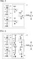
- FIG. 3 illustrates, in schematic form, one embodiment of trigger circuit 28 coupled to provide TRIGGER to the control electrode of clamping device 26.
- RC timer 32 includes a capacitive element 42 and a resistive element 44.
- Capacitive element 42 has a first terminal coupled to VDD and a second terminal coupled to a circuit node 41, which provides an output of RC timer 32.
- Resistive element 44 has a first terminal coupled to node 41 and a second terminal coupled to VSS. (Note that in FIGS. 3-6 , VSS is denoted with the ground symbol.)
- RC timer 34 includes a capacitive element 46 and a resistive element 48.
- Capacitive element 46 has a first terminal coupled to BOOST and a second terminal coupled to a circuit node 47, which provides an output of RC timer 34.
- Resistive element 48 has a first terminal coupled to node 47 and a second terminal coupled to VSS.
- RC timers 32 and 34 are implemented as high pass filters in which RC timer 32 is a high pass filter with input coupled to VDD and RC timer 34 is a high pass filter with input coupled to BOOST.
- the use of high pass filters help to discriminate between a normal rise in VDD or BOOST (e.g. a normal power-up event) versus a fast stress event that is not normal, and which can result in damage of the electronic circuits coupled to VDD or BOOST.
- Logic circuit 36 of FIG. 3 includes a NOR gate 50 and an inverter 52.
- Circuit node 41 (the output of RC timer 32) is coupled to a first input of NOR gate 50 and circuit node 47 (the output of RC timer 34) is coupled to a second input of NOR gate 50.
- An input of inverter 52 is coupled to an output of NOR gate 50 and an output of inverter 52 drives the control electrode of clamping device 26 via TRIGGER.
- Each of NOR gate 50 and inverter 52 is coupled to BOOST and VSS, therefore, these gates are powered by BOOST.
- logic circuit 36 of FIG. 3 receives the output of both RC timers 32 and 34. Therefore, when RC timer 32 detects a rapid voltage rise on VDD, circuit node 41 increases, and when RC timer 34 detects a rapid voltage rise on BOOST, circuit node 47 increases. That is, each RC timer is a detection circuit of rapid voltage increases on corresponding voltage supply nodes, VDD and BOOST. Rapid voltage increase on VDD indicates a TES event on VDD 12 and rapid voltage increase on BOOST indicates a TES event on I/O pad 14. Initially, prior to any TES events, such as during normal operation, the output of NOR gate 50 is at logic level high (since circuit nodes 41 and 47 are low). This maintains clamping device 26 in an off state.
- FIG. 4 illustrates, in schematic form, a more detailed representation of logic circuit 36 of FIG. 3 .
- NOR gate 50 includes a ballast element 54 (shown in the form of a resistor), an N-channel MOS transistor 56, and an N-channel MOS transistor 58.
- a first terminal of ballast element 54 is coupled to BOOST and a second terminal of ballast element 54 is coupled to a circuit node 55 (which corresponds to the output of NOR gate 50).
- a first current electrode of transistor 56 is coupled to node 55, a second current electrode of transistor 56 is coupled to VSS, and a control electrode of transistor 56 (corresponding to the second input of NOR gate 50) is coupled to circuit node 47.
- a first current electrode of transistor 58 is coupled to node 55, a second current electrode of transistor 58 is coupled to VSS, and a control electrode of transistor 58 (corresponding to the first input of NOR gate 50) is coupled to node 41.
- Inverter 52 includes a P-channel transistor 60 and a ballast element 62 (shown in the form of a resistor).
- a first current electrode of transistor 60 is coupled to BOOST, a control electrode of transistor 60 is coupled to node 55, and a second current electrode is coupled to a circuit node 61.
- a first terminal of ballast element 62 is coupled to node 61 and a second terminal of ballast element 62 is coupled to VSS.
- Note 61 is coupled to the control electrode of clamping device 26.
- FIG. 5 illustrates in schematic form, another embodiment of trigger circuit 28 coupled to provide TRIGGER to the control electrode of clamping device 26.
- RC timer 32 includes a capacitive element 70 and a resistive element 72.
- Capacitive element 70 has a first terminal coupled to VDD and a second terminal coupled to a circuit node 71, which provides an output of RC timer 32.
- Resistive element 72 has a first terminal coupled to node 71 and a second terminal coupled to VSS.
- RC timer 34 includes a capacitive element 74 and a resistive element 76.
- Capacitive element 74 has a first terminal coupled to BOOST and a second terminal coupled to a circuit node 75, which provides an output of RC timer 34.
- Resistive element 76 has a first terminal coupled to node 75 and a second terminal coupled to VSS.
- RC timers 32 and 34 are implemented as high pass filters in which RC timer 32 is a high pass filter with input coupled to VDD and RC timer 34 is a high pass filter with input coupled to by BOOST.
- Logic circuit 36 of FIG. 5 includes inverters 78 and 80 and a NAND gate 82.
- Circuit node 71 (the output of RC timer 32) is coupled to an input of inverter 80 and circuit node 75 (the output of RC timer 34) is coupled to an input of inverter 78.
- An output of inverter 78 is coupled to a first input of NAND gate 82, and an output of inverter 80 is coupled to a second input of NAND gate 82.
- An output of NAND gate 82 provides TRIGGER to the control electrode of clamping device 26.
- Inverter 78 is coupled to BOOST and VSS and therefore powered by BOOST
- inverter 80 is coupled to VDD and VSS and therefore powered by VDD.
- NAND gate 82 is coupled to BOOST, VDD, and VSS and therefore is partially powered by BOOST and partially powered by VDD, as will be seen in more detail in FIG. 6 .
- logic circuit 36 of FIG. 5 receives the output of both RC timers 32 and 34. Therefore, when RC timer 32 detects a rapid voltage rise on VDD, the voltage of circuit node 71 increases, and when RC timer 34 detects a rapid voltage rise on BOOST, the voltage of circuit node 75 increases. That is, each RC timer is a detection circuit of rapid voltage increases on corresponding voltage supplies, VDD and BOOST. As stated above, a rapid voltage increase on VDD indicates a TES event on VDD 12, and a rapid voltage increase on BOOST indicates a TES event on I/O pad 14.
- FIG. 6 illustrates, in schematic form, a more detailed representation of logic circuit 36 of FIG. 5 .
- Inverter 80 includes a ballast element 84 (shown in the form of a resistor) and an N-channel MOS transistor 86.
- a first terminal of ballast element 84 is coupled to VDD, and a second terminal of ballast element 84 is coupled to a circuit node 85, which corresponds to the output of inverter 80.
- a first current electrode of transistor 86 is coupled to node 85, a second current electrode of transistor 86 is coupled to VSS, and a control electrode of transistor 86 is coupled to circuit node 71 and corresponds to the input of inverter 80.
- Inverter 78 includes a ballast element 92 (shown in the form of a resistor) and an N-channel MOS transistor 94.
- a first terminal of ballast element 92 is coupled to BOOST, and a second terminal of ballast element 92 is coupled to a circuit node 93, which corresponds to the output of inverter 78.
- a first current electrode of transistor 94 is coupled to node 93, a second current electrode of transistor 94 is coupled to VSS, and a control electrode of transistor 94 is coupled to circuit node 75 and corresponds to the input of inverter 78.
- NAND gate 82 includes P-channel MOS transistors 88 and 96 and ballast elements 90 and 98 (shown in the form of resistors).
- a first current electrode of transistor 88 is coupled to VDD, a second current electrode of transistor 88 is coupled to a circuit node 89, and a control electrode of transistor 88 is coupled to node 85 and corresponds to the second input of NAND gate 82.
- a first terminal of ballast element 90 is coupled to node 89, which corresponds to the output of NAND gate 82, and a second terminal of ballast element 90 is coupled to VSS.
- a first current electrode of transistor 96 is coupled to BOOST, a second current electrode of transistor 96 is coupled to a circuit node 89, and a control electrode of transistor 96 is coupled to node 93 and corresponds to the first input of NAND gate 82.
- a first terminal of ballast element 98 is coupled to node 89, which corresponds to the output of NAND gate 82, and a second terminal of ballast element 98 is coupled to VSS.
- the trigger circuits of FIGs 3 and 4 have their logic circuit 36 powered solely by the BOOST supply. This means that the gate voltage of the clamping device would be limited to the BOOST voltage during a TES event occurring on VDD, and the BOOST voltage is typically lower than the VDD voltage for such an event. However, the main benefit of these trigger circuits, which is a reduced trigger activation voltage for such a TES event, is still effective due to the additional detection stage powered by VDD.
- the trigger circuits of FIGs. 5 and 6 have their logic circuit 36 powered by VDD and BOOST and are therefore capable of driving the gate of the clamping device to either the VDD or the BOOST voltage, depending on whether the TES event is detected on VDD or BOOST, respectively. Therefore, these trigger circuits may also be able to provide a higher maximum gate voltage to the clamping device during a TES event on VDD, in addition to the benefit of a reduced trigger activation voltage.
- resistive element 44, 48, 72, and 76 can be implemented with one or more resistive elements in series or in parallel.
- resistive elements 44, 48, 72, and 76 can be implemented with a resistive ladder or resistive pull-down network with a programmable resistive value in which the resistance can be set depending on the operating state of IC 10. While ballast elements 54, 62, 84, 90, 92, and 98 described above are shown as resistors in the embodiments of FIGs. 4 and 6 , other devices may be used, such as, for example, complementary MOS transistors or other types of resistive elements.
- logic circuit 36 may include a different number of logic gate stages (e.g. one or more), such as inverter stages.
- a P-channel MOS device can be used as clamp device 26 rather than an N-channel MOS device.
- different logic gates may be used to implement the logic function of logic circuit 36.
- different circuit configurations can be used to implement the logic gates of logic circuit 36 in which logic circuit 36 activates clamping device 26 upon the detection of a TES event either on VDD or BOOST.
- Coupled is not intended to be limited to a direct coupling or a mechanical coupling.
- an integrated circuit for protecting against transient electrical stress events includes a trigger circuit including a first detection circuit coupled to a first supply voltage; a second detection circuit coupled to a second supply voltage; a rail clamp device, wherein during a first type of electrical stress event, the rail clamp device is activated in response to a first output signal provided by the first detection circuit, and during a second type of electrical stress event, the rail clamp device is activated in response to a second output signal provided by the second detection circuit.
- the first detection circuit includes a first capacitive element coupled in series with a first resistive element between the first supply voltage and a third supply voltage, and an output terminal between the first capacitive element and the first resistive element provides the first output signal
- the second detection circuit includes a second capacitive element coupled in series with a second resistive element between the second supply voltage and the third supply voltage, and an output terminal between the second capacitive element and the second resistive element provides the second output signal.
- the integrated circuit further includes a combinatorial logic circuit coupled between the first and second detection circuits and the rail clamp device, wherein the combinatorial logic circuit is configured to receive the first output signal of the first detection circuit and the second output signal of the second detection circuit, and generate a third output signal that activates the rail clamp device when the first or second output signals of the first or second detection circuits detect an electrical stress event.
- the combinatorial logic circuit includes a NOR gate having a first input coupled to the first output signal of the first detection circuit and a second input coupled to the second output signal of the second detection circuit.
- the combinatorial logic circuit further includes an inverter having an input coupled to an output of the NOR gate and an output configured to control the rail clamp device.
- the NOR gate includes a first ballast element including a first terminal coupled to the second supply voltage and a second terminal; a first metal-oxide semiconductor (MOS) transistor including a first current electrode coupled to the second terminal of the first resistive element, a second current electrode coupled to a third voltage supply and a gate electrode coupled to the output signal of the second detection circuit; and a second MOS transistor including a first current electrode coupled to the second terminal of the first resistive element, a second current electrode coupled to the third voltage supply and a gate electrode coupled to the output signal of the first detection circuit.
- MOS metal-oxide semiconductor
- the inverter includes a third MOS transistor having a first current electrode coupled to the second supply voltage, a second current electrode coupled to a first terminal of a second ballast element, and a gate electrode coupled to the first current electrodes of the first and second MOS transistors; and the second resistive element includes a second terminal coupled to the third voltage supply.
- the integrated circuit further includes a combinatorial logic circuit including a first inverter including an input coupled to the first output signal of the first detection circuit; a second inverter including an input coupled to the second output signal of the second detection circuit; and a NAND gate that generates a third output signal, wherein the NAND gate includes a first input configured to receive an output signal from the first inverter, and a second input configured to receive an output signal from the second inverter.
- the first inverter includes a third ballast element coupled in series with a first MOS transistor between the first supply voltage and the third supply voltage, wherein a gate electrode of the first MOS transistor is coupled to the first output signal
- the second inverter includes a fourth ballast element coupled in series with a second MOS transistor between the second supply voltage and the third supply voltage, wherein a gate electrode of the second MOS transistor is coupled to the second output signal.
- the NAND gate includes a third inverter including a fifth ballast element coupled in series with a third MOS transistor between the first supply voltage and the third supply voltage, wherein a gate electrode of the third MOS transistor is coupled to the output signal from the first inverter, and the fourth inverter includes a sixth ballast element coupled in series with a fourth MOS transistor between the second supply voltage and the third supply voltage, wherein a gate electrode of the fourth MOS transistor is coupled to the output signal from the second inverter.
- a method in another embodiment, includes detecting a first type of electrical stress event with a first detection circuit in a trigger circuit, wherein the first detection circuit is coupled to a first supply voltage; when the first type of electrical stress event is detected, activating a rail clamp device to protect an integrated circuit from the first type of transient electrical stress event; detecting a second type of electrical stress event with a second detection circuit in the trigger circuit, wherein the second detection circuit is coupled to a second supply voltage; and when the second type of electrical event is detected, activating the rail clamp device to protect the integrated circuit from the second type of transient electrical stress event.
- the method further includes generating an output signal with a combinatorial logic circuit coupled to receive input from the first and second detection circuits, and to provide the output signal to activate the rail clamp device based on the input from the first and second detection circuits.
- the method further includes receiving an output signal from the first detection circuit at an input to a NOR gate; receiving an output signal from the second detection circuit at another input to the NOR gate; receiving an output signal from the NOR gate at an input to an inverter; activating the rail clamp device with an output of the inverter.
- the method further includes receiving an output signal from the first detection circuit at an input to a first inverter; receiving an output signal from the second detection circuit at an input to a second inverter; receiving an output signal from the first inverter at an input to a NAND gate; receiving an output signal from the second inverter at another input to the NAND gate; activating the rail clamp device with an output of the NAND gate.
- an integrated circuit for protecting against transient electrical stress events includes a trigger circuit including a first resistive-capacitive (RC) filter coupled to a first supply voltage; a second RC filter coupled to a second supply voltage; combinatorial logic circuit configured to receive an output signal from the first RC filter, receive an output signal from the second RC filter, and generate an output signal that activates a rail clamp device when the output signal from the first or second RC filters indicate an electrical stress event.
- the combinatorial logic circuit includes a NOR gate having a first input coupled to the output signal of the first RC filter and a second input coupled to the output signal of the second RC filter.
- the combinatorial logic circuit further includes an inverter having an input coupled to an output of the NOR gate and an output configured to control the rail clamp device.
- the NOR gate includes a first ballast element including a first terminal coupled to the second supply voltage and a second terminal; a first metal-oxide semiconductor (MOS) transistor including a first current electrode coupled to the second terminal of the first resistive element, a second current electrode coupled to a third supply voltage and a gate electrode coupled to the output signal of the second RC filter; and a second MOS transistor including a first current electrode coupled to the second terminal of the resistive element, a second current electrode coupled to the third supply voltage and a gate electrode coupled to the output signal of the first RC filter; and the inverter includes a third MOS transistor having a first current electrode coupled to the second supply voltage, a second current electrode coupled to a first terminal of a second ballast element, and a gate electrode coupled to the first current electrodes of the first and second MOS transistors; and
- the combinatorial logic circuit further includes a first inverter including an input coupled to the output signal of the first RC filter; a second inverter including an input coupled to the output signal of the second RC filter; and a NAND gate that generates an output signal to activate the rail clamp device, wherein the NAND gate includes a first input configured to receive an output signal from the first inverter, and a second input configured to receive an output signal from the second inverter.
- the first inverter includes a first ballast element coupled in series with a first MOS transistor between the first supply voltage and ground, wherein a gate electrode of the first MOS transistor is coupled to the first output signal
- the second inverter includes a second ballast element coupled in series with a second MOS transistor between the second supply voltage and ground, wherein a gate electrode of the second MOS transistor is coupled to the second output signal
- the NAND gate includes: a third inverter including a third ballast element coupled in series with a third MOS transistor between the first supply voltage and ground, wherein a gate electrode of the third MOS transistor is coupled to the output signal from the first inverter
- the fourth inverter includes a fourth ballast element coupled in series with a fourth MOS transistor between the second supply voltage and ground, wherein a gate electrode of the fourth MOS transistor is coupled to the output signal from the second inverter.
- An integrated circuit with protection against transient electrical stress events includes a trigger circuit having a first detection circuit coupled to a first supply voltage, a second detection circuit coupled to a second supply voltage, and a rail clamp device.
- the rail clamp device is activated in response to a first output signal provided by the first detection circuit.
- the rail clamp device is activated in response to a second output signal provided by the second detection circuit.
Landscapes
- Engineering & Computer Science (AREA)
- Microelectronics & Electronic Packaging (AREA)
- Physics & Mathematics (AREA)
- Computer Hardware Design (AREA)
- Computing Systems (AREA)
- General Engineering & Computer Science (AREA)
- Mathematical Physics (AREA)
- Semiconductor Integrated Circuits (AREA)
- Power Engineering (AREA)
- Electronic Switches (AREA)
- Logic Circuits (AREA)
Abstract
Description
- This disclosure relates generally to integrated circuits (ICs), and more specifically, to protection from transient electrical stress (TES) events for integrated circuits.
- Electronic circuits are designed to operate over limited voltage ranges. Exposure to voltages beyond those limited voltage ranges can damage or destroy those circuits. The problem is particularly notable for integrated circuits, which often have many external terminals connected to circuitry fabricated on a very small scale.
- Transient voltage suppression circuits for integrated circuits should function for both unpowered transient events (i.e., those transient events occurring when the integrated circuit is not powered up for normal operation) and powered transient events (i.e., those transient events occurring when power is applied to the integrated circuit for normal operation). Unpowered TES events may include, but are not limited to, Electrostatic Discharge events (ESD), for example Human Body Model (HBM), Machine Model, or Charged Device Model (CDM) events. Powered TES events may include, but are not limited to, Powered ESD (PESD), Electric Fast Transient (EFT), Power Surge, or Ring Wave events.
- Various aspects of the disclosure are defined in the accompanying claims. In a first aspect, there is defined an integrated circuit for protecting against transient electrical stress events, comprising: a trigger circuit including: a first detection circuit coupled to a first supply voltage; a second detection circuit coupled to a second supply voltage; a rail clamp device, wherein during a first type of electrical stress event, the rail clamp device is activated in response to a first output signal provided by the first detection circuit, and during a second type of electrical stress event, the rail clamp device is activated in response to a second output signal provided by the second detection circuit.
- The present invention is illustrated by way of example and is not limited by the accompanying figures, in which like references indicate similar elements. Elements in the figures are illustrated for simplicity and clarity and have not necessarily been drawn to scale.
-
FIG. 1 illustrates, in partial schematic and partial block diagram form, an integrated circuit having TES event protection circuitry, in accordance with one embodiment of the present invention. -
FIG. 2 illustrates, in partial schematic and partial block diagram form, one embodiment of a trigger circuit of TES event protection circuitry ofFIG. 1 . -
FIGS. 3 - 6 illustrate, in schematic form, further details of various embodiments of the trigger circuit ofFIG. 2 . - A transient electrical stress (TES) event refers to a fast rise in voltage at a net inside an electronic circuit which may result in damage or destruction of electronic circuits coupled to that net. Therefore, with TES event protection circuitry, a trigger circuit detects a transient voltage increase corresponding to a TES event, and, in response, places a clamping device into a conductive state to provide a current path to safely dissipate the associated stress current and to limit the transient voltage during the TES event. A large MOS device is often used as the clamping device between two supply rails, and the conductivity of the large MOS device is controlled by the trigger circuit. In many cases, an array of large MOS clamping devices is used with their gate terminals biased by a shared trigger circuit. During a TES event, it is desirable that the MOS clamping device does not reach its breakdown voltage as this may lead to the destruction of the clamping device and therefore cause permanent damage to the electronic circuit. However, in some applications, the normal operating voltage and the breakdown voltage of the MOS clamping device are very close, thus the design margin for the trigger circuit activating before the MOS device goes into breakdown is very tight, limiting the ability of the MOS device to operate as a clamping device.
- Furthermore, in boosted designs of TES event protection circuitry, a separate (boosted) supply is used for powering the trigger circuit. All external pads, including I/O and power supply pads, are coupled to this boosted supply via pull-up diodes, ensuring that the boosted supply carries the highest possible potential. During normal operation of the electronic circuit, the boosted supply is typically charged up to the voltage level of the main power supply. If a TES event occurs on an I/O pin, the voltage on the boosted supply is elevated above the main power supply, which carries most of the TES current and connects to the drain terminal of the clamping device. Therefore, the trigger circuit can provide a gate voltage to the clamping device higher than the voltage on its drain. Overdriving the gate of the clamping device increases its on-conductance and therefore its TES protection efficiency. This improves design margins for TES events which occur on an I/O pad, resulting in a greater margin between the peak stress voltage and the breakdown voltage of the clamping device or any other device coupled to the stressed I/O pad (for example, input or output buffers) or coupled to the main power supply.
- However, if the TES event occurs directly on the main power supply (i.e. at the drain of the clamping device), the supply voltage to the trigger circuit may be lower than the voltage across the clamping device, making the design margin of conventional boosted designs worse as compared to non-boosted designs. Furthermore, during a powered TES event on the main power supply, the overvoltage level on the main power supply needed to activate the trigger circuit via the boosted supply is higher as compared to non-boosted designs. This is because the boosted supply voltage is reduced by the pull-up diode from the main power supply. The resulting activation voltage for a TES event on the main power supply can be higher than the breakdown voltage of the clamping device, which may cause its destruction.
- Therefore, as will be described below, a trigger circuit having multiple filters coupled to different supply voltages is used to activate the clamping device. In this manner, the trigger circuit can be designed to activate when any of the different supply voltages experiences a fast rising voltage ramp without causing damage to the electronic circuit. Furthermore, the TES event protection circuitry described below functions for both powered and unpowered transient events.
-
FIG. 1 illustrates anintegrated circuit 10 having a boosted TES protection scheme. IC 10 includes a first power supply rail (VDD) 12, a firstpower supply pad 13 coupled to VDD 12, an I/O pad 14, a second power supply rail (VSS) 16, a secondpower supply pad 15 coupled toVSS 16, aboost bus 11, atrigger circuit 28, aclamping device 26, anddiodes Clamping device 26 may be an N-channel metal oxide semiconductor field effect transistor (MOSFET or MOS transistor).Boost bus 11 is coupled totrigger circuit 28 to provide a third power supply BOOST to triggercircuit 28.Diode 22 has an anode coupled toVSS 16 and a cathode coupled to I/O pad 14, to an anode ofdiode 18. A cathode ofdiode 18 is coupled to boostbus 11. An anode ofdiode 20 is coupled to I/O pad 14, and a cathode ofdiode 20 is coupled to VDD 12. A first current electrode ofclamping device 26 is coupled to VDD 12, a second current electrode ofclamping device 26 is coupled toVSS 16, and a control electrode ofclamping device 26 is coupled to receive a signal, TRIGGER, fromtrigger circuit 28.Trigger circuit 28 is also coupled to VDD 12 andVSS 16. An anode ofdiode 24 is coupled to VDD 12 and a cathode ofdiode 24 is coupled to boostbus 11. - In operation, circuits coupled to I/
O pad 14 are protected by diodes, which shunt any TES current toVSS 16 or VDD 12, depending on the polarity of the TES event.Diode 22 conducts any TES current that leaves I/O pad 14.Diode 20 andclamping device 26 are the primary shunt path for TES current injected into I/O pad 14. During a stress event that injects current into I/O pad 14,trigger circuit 28 drives the control electrode ofclamping device 26 to a voltage level needed forclamping device 26 to shunt the TES current between VDD 12 andVSS 16. During such stress event, a large TES current flows through VDD supply rail 12. Because of the resistive voltage drop in the VDD supply rail, the supply voltage will vary with position, i.e. it will decrease over distance to the stressed I/O pad. The supply voltage VDD will be highest atdiode 20. - In the boosted protection scheme of
FIG. 1 ,boost bus 11 is powered from I/O pad 14 during a TES event that injects current into I/O pad 14.Diode 18 andboost bus 11 are designed to have a lower resistive voltage drop thandiode 20 and VDD supply rail 12 so thatboost bus 11 can provide a higher supply voltage, at node BOOST, to triggercircuit 28. This is mainly due to the fact that there is little current flowing throughdiode 18 and boostbus 11 as they are not part of the primary TES current dissipation path. In this manner, a higher voltage is provided to the control electrode ofclamping device 26 by the trigger circuit, allowingclamping device 26 to be made smaller to achieve a similar on-conductance compared to a non-boosted design where the trigger circuit would be powered directly by the VDD supply rail. - A drawback of this topology is that when TES current is injected directly onto VDD 12,
boost bus 11 is powered from VDD 12, throughdiode 24. In general, the trigger circuit gets activated by a fast rising supply voltage that exceeds the activation voltage of the trigger circuit. The voltage drop indiode 24 reduces the supply voltage at node BOOST to triggercircuit 28 during a TES event. During normal, power-up operation of the electronic circuit, when no TES event is occurring,boost bus 11 is typically charged up to the voltage level of VDD 12. Therefore, the overvoltage on the VDD supply during a TES event needed to activate the trigger circuit thoughdiode 24 is increased compared to a non-boosted design. However, by using separate filters intrigger circuit 28 powered separately by VDD 12 and BOOST,trigger circuit 28 can effectively provide TES protection when a TES event occurs on either VDD 12 or I/O pad 14. -
FIG 2 illustrates in partial schematic and partial block diagram form,trigger circuit 28 ofFIG. 1 .Trigger circuit 28 includes a resistor-capacitor (RC)timer 32, anRC timer 34, and alogic circuit 36. In the illustrated embodiment,RC timer 32 is implemented as afilter 38, andRC timer 34 is implemented as afilter 40.RC timers FIG. 2 is clampingdevice 26.Logic circuit 36 is coupled to BOOST (which may be coupled to boost bus 11) and VSS (which may be coupled to VSS 16). In some embodiments,logic circuit 36 may also be coupled to VDD (which may be coupled to VDD 12) in addition to BOOST and VSS.Logic circuit 36 has a first input coupled to filter 40, a second input coupled to filter 38, and an output coupled to provide a trigger signal on the TRIGGER node to the control electrode of clampingdevice 26.Filter 38 is coupled to VDD and VSS and provides an output to the second input oflogic circuit 36.Filter 40 is coupled to BOOST and VSS and provides an output to the first input oflogic circuit 36. - In operation, each
filter device 26 when either supply experiences a fast rising voltage ramp above the activation voltage of the trigger circuit, due, for example, to a TES event. In this manner, with a boosted design where part oftrigger circuit 28 is powered by a BOOST supply,trigger circuit 28 can be used to improve triggering for TES events at I/O pad 14 (in which BOOST is higher than VDD) without negatively impacting the trigger circuit activation for TES events at VDD (in which BOOST is lower than VDD). In the former case,trigger circuit 28 is activated via BOOST, and in the latter case,trigger circuit 28 is activated via VDD. Note that BOOST is typically charged up to VDD during normal operation (when a TES event is not occurring). However, during a TES event, BOOST is decoupled from VDD, and the logical combination of the outputs offilters logic circuit 36 determines the activation of clampingdevice 26. In one embodiment,logic circuit 36 effectively ORs the outputs offilters device 26 is activated or turned on to shunt TES current between VDD and VSS. Specific examples ofRC timers logic circuit 26 will be provided inFIGS. 3-6 below. -
FIG. 3 illustrates, in schematic form, one embodiment oftrigger circuit 28 coupled to provide TRIGGER to the control electrode of clampingdevice 26.RC timer 32 includes acapacitive element 42 and aresistive element 44.Capacitive element 42 has a first terminal coupled to VDD and a second terminal coupled to acircuit node 41, which provides an output ofRC timer 32.Resistive element 44 has a first terminal coupled tonode 41 and a second terminal coupled to VSS. (Note that inFIGS. 3-6 , VSS is denoted with the ground symbol.)RC timer 34 includes acapacitive element 46 and aresistive element 48.Capacitive element 46 has a first terminal coupled to BOOST and a second terminal coupled to acircuit node 47, which provides an output ofRC timer 34.Resistive element 48 has a first terminal coupled tonode 47 and a second terminal coupled to VSS. Note that, as inFIG. 2 ,RC timers RC timer 32 is a high pass filter with input coupled to VDD andRC timer 34 is a high pass filter with input coupled to BOOST. The use of high pass filters help to discriminate between a normal rise in VDD or BOOST (e.g. a normal power-up event) versus a fast stress event that is not normal, and which can result in damage of the electronic circuits coupled to VDD or BOOST. -
Logic circuit 36 ofFIG. 3 includes a NORgate 50 and aninverter 52. Circuit node 41 (the output of RC timer 32) is coupled to a first input of NORgate 50 and circuit node 47 (the output of RC timer 34) is coupled to a second input of NORgate 50. An input ofinverter 52 is coupled to an output of NORgate 50 and an output ofinverter 52 drives the control electrode of clampingdevice 26 via TRIGGER. Each of NORgate 50 andinverter 52 is coupled to BOOST and VSS, therefore, these gates are powered by BOOST. - In operation,
logic circuit 36 ofFIG. 3 receives the output of bothRC timers RC timer 32 detects a rapid voltage rise on VDD,circuit node 41 increases, and whenRC timer 34 detects a rapid voltage rise on BOOST,circuit node 47 increases. That is, each RC timer is a detection circuit of rapid voltage increases on corresponding voltage supply nodes, VDD and BOOST. Rapid voltage increase on VDD indicates a TES event on VDD 12 and rapid voltage increase on BOOST indicates a TES event on I/O pad 14. Initially, prior to any TES events, such as during normal operation, the output of NORgate 50 is at logic level high (sincecircuit nodes device 26 in an off state. However, the first ofcircuit nodes gate 50 to go low. This results in the output ofinverter 52 going high and thus turning on (i.e. activating) clampingdevice 26 for the detected TES event. -
FIG. 4 illustrates, in schematic form, a more detailed representation oflogic circuit 36 ofFIG. 3 . NORgate 50 includes a ballast element 54 (shown in the form of a resistor), an N-channel MOS transistor 56, and an N-channel MOS transistor 58. A first terminal ofballast element 54 is coupled to BOOST and a second terminal ofballast element 54 is coupled to a circuit node 55 (which corresponds to the output of NOR gate 50). A first current electrode oftransistor 56 is coupled tonode 55, a second current electrode oftransistor 56 is coupled to VSS, and a control electrode of transistor 56 (corresponding to the second input of NOR gate 50) is coupled tocircuit node 47. A first current electrode oftransistor 58 is coupled tonode 55, a second current electrode oftransistor 58 is coupled to VSS, and a control electrode of transistor 58 (corresponding to the first input of NOR gate 50) is coupled tonode 41.Inverter 52 includes a P-channel transistor 60 and a ballast element 62 (shown in the form of a resistor). A first current electrode oftransistor 60 is coupled to BOOST, a control electrode oftransistor 60 is coupled tonode 55, and a second current electrode is coupled to acircuit node 61. A first terminal ofballast element 62 is coupled tonode 61 and a second terminal ofballast element 62 is coupled to VSS. Note 61 is coupled to the control electrode of clampingdevice 26. -
FIG. 5 illustrates in schematic form, another embodiment oftrigger circuit 28 coupled to provide TRIGGER to the control electrode of clampingdevice 26.RC timer 32 includes acapacitive element 70 and aresistive element 72.Capacitive element 70 has a first terminal coupled to VDD and a second terminal coupled to acircuit node 71, which provides an output ofRC timer 32.Resistive element 72 has a first terminal coupled tonode 71 and a second terminal coupled to VSS.RC timer 34 includes acapacitive element 74 and aresistive element 76.Capacitive element 74 has a first terminal coupled to BOOST and a second terminal coupled to acircuit node 75, which provides an output ofRC timer 34.Resistive element 76 has a first terminal coupled tonode 75 and a second terminal coupled to VSS. Note that, as inFIGs. 2 and3 ,RC timers RC timer 32 is a high pass filter with input coupled to VDD andRC timer 34 is a high pass filter with input coupled to by BOOST. -
Logic circuit 36 ofFIG. 5 includesinverters NAND gate 82. Circuit node 71 (the output of RC timer 32) is coupled to an input ofinverter 80 and circuit node 75 (the output of RC timer 34) is coupled to an input ofinverter 78. An output ofinverter 78 is coupled to a first input ofNAND gate 82, and an output ofinverter 80 is coupled to a second input ofNAND gate 82. An output ofNAND gate 82 provides TRIGGER to the control electrode of clampingdevice 26.Inverter 78 is coupled to BOOST and VSS and therefore powered by BOOST, andinverter 80 is coupled to VDD and VSS and therefore powered by VDD.NAND gate 82 is coupled to BOOST, VDD, and VSS and therefore is partially powered by BOOST and partially powered by VDD, as will be seen in more detail inFIG. 6 . - In operation,
logic circuit 36 ofFIG. 5 receives the output of bothRC timers RC timer 32 detects a rapid voltage rise on VDD, the voltage ofcircuit node 71 increases, and whenRC timer 34 detects a rapid voltage rise on BOOST, the voltage ofcircuit node 75 increases. That is, each RC timer is a detection circuit of rapid voltage increases on corresponding voltage supplies, VDD and BOOST. As stated above, a rapid voltage increase on VDD indicates a TES event on VDD 12, and a rapid voltage increase on BOOST indicates a TES event on I/O pad 14. Initially, prior to any TES events, such as during normal operation, the outputs ofinverters NAND gate 82 is low. This maintains clampingdevice 26 in an off state. However, the first ofcircuit nodes respective inverter NAND gate 82 to go high. This results in turning on (i.e. activating) clampingdevice 26 for the detected TES event. -
FIG. 6 illustrates, in schematic form, a more detailed representation oflogic circuit 36 ofFIG. 5 .Inverter 80 includes a ballast element 84 (shown in the form of a resistor) and an N-channel MOS transistor 86. A first terminal ofballast element 84 is coupled to VDD, and a second terminal ofballast element 84 is coupled to acircuit node 85, which corresponds to the output ofinverter 80. A first current electrode oftransistor 86 is coupled tonode 85, a second current electrode oftransistor 86 is coupled to VSS, and a control electrode oftransistor 86 is coupled tocircuit node 71 and corresponds to the input ofinverter 80.Inverter 78 includes a ballast element 92 (shown in the form of a resistor) and an N-channel MOS transistor 94. A first terminal ofballast element 92 is coupled to BOOST, and a second terminal ofballast element 92 is coupled to acircuit node 93, which corresponds to the output ofinverter 78. A first current electrode oftransistor 94 is coupled tonode 93, a second current electrode oftransistor 94 is coupled to VSS, and a control electrode oftransistor 94 is coupled tocircuit node 75 and corresponds to the input ofinverter 78.NAND gate 82 includes P-channel MOS transistors ballast elements 90 and 98 (shown in the form of resistors). A first current electrode oftransistor 88 is coupled to VDD, a second current electrode oftransistor 88 is coupled to acircuit node 89, and a control electrode oftransistor 88 is coupled tonode 85 and corresponds to the second input ofNAND gate 82. A first terminal ofballast element 90 is coupled tonode 89, which corresponds to the output ofNAND gate 82, and a second terminal ofballast element 90 is coupled to VSS. A first current electrode oftransistor 96 is coupled to BOOST, a second current electrode oftransistor 96 is coupled to acircuit node 89, and a control electrode oftransistor 96 is coupled tonode 93 and corresponds to the first input ofNAND gate 82. A first terminal ofballast element 98 is coupled tonode 89, which corresponds to the output ofNAND gate 82, and a second terminal ofballast element 98 is coupled to VSS. - The trigger circuits of
FIGs 3 and 4 have theirlogic circuit 36 powered solely by the BOOST supply. This means that the gate voltage of the clamping device would be limited to the BOOST voltage during a TES event occurring on VDD, and the BOOST voltage is typically lower than the VDD voltage for such an event. However, the main benefit of these trigger circuits, which is a reduced trigger activation voltage for such a TES event, is still effective due to the additional detection stage powered by VDD. The trigger circuits ofFIGs. 5 and 6 , on the other hand, have theirlogic circuit 36 powered by VDD and BOOST and are therefore capable of driving the gate of the clamping device to either the VDD or the BOOST voltage, depending on whether the TES event is detected on VDD or BOOST, respectively. Therefore, these trigger circuits may also be able to provide a higher maximum gate voltage to the clamping device during a TES event on VDD, in addition to the benefit of a reduced trigger activation voltage. - In alternate embodiments, different circuit elements or configurations may be used for
trigger circuit 28. For example,resistive element resistive elements IC 10. Whileballast elements FIGs. 4 and6 , other devices may be used, such as, for example, complementary MOS transistors or other types of resistive elements. Also, in an alternate embodiment, the positions of the capacitive element and resistive element infilters logic circuit 36 may include a different number of logic gate stages (e.g. one or more), such as inverter stages. In another alternate embodiment, a P-channel MOS device can be used asclamp device 26 rather than an N-channel MOS device. Also, different logic gates may be used to implement the logic function oflogic circuit 36. Similarly, different circuit configurations can be used to implement the logic gates oflogic circuit 36 in whichlogic circuit 36 activates clampingdevice 26 upon the detection of a TES event either on VDD or BOOST. - Therefore, by now it can be understood how the use of two separate RC filters coupled to different power supply voltages can be used to provide a protection system which is effective for protecting against TES events on both VDD and I/O pads. In this manner, the benefits of a boosted design can be achieved, such as higher design margins, while still effectively detecting TES events on VDD. Furthermore, the protection circuits described herein protect against both powered and unpowered TES events.
- Because the apparatus implementing the present invention is, for the most part, composed of electronic components and circuits known to those skilled in the art, circuit details will not be explained in any greater extent than that considered necessary as illustrated above, for the understanding and appreciation of the underlying concepts of the present invention and in order not to obfuscate or distract from the teachings of the present invention.
- Although the invention has been described with respect to specific conductivity types or polarity of potentials, skilled artisans appreciated that conductivity types and polarities of potentials may be reversed.
- Those skilled in the art will recognize that boundaries between the functionality of the above described blocks and operations merely illustrative. The functionality of multiple operations may be combined into a single operation, and/or the functionality of a single operation may be distributed in additional operations. Moreover, alternative embodiments may include multiple instances of a particular operation, and the order of operations may be altered in various other embodiments.
- Although the invention is described herein with reference to specific embodiments, various modifications and changes can be made without departing from the scope of the present invention as set forth in the claims below. For example, different detection circuits can be used in place of
RC timers - The term "coupled," as used herein, is not intended to be limited to a direct coupling or a mechanical coupling.
- Furthermore, the terms "a" or "an," as used herein, are defined as one or more than one. Also, the use of introductory phrases such as "at least one" and "one or more" in the claims should not be construed to imply that the introduction of another claim element by the indefinite articles "a" or "an" limits any particular claim containing such introduced claim element to inventions containing only one such element, even when the same claim includes the introductory phrases "one or more" or "at least one" and indefinite articles such as "a" or "an." The same holds true for the use of definite articles.
- Unless stated otherwise, terms such as "first" and "second" are used to arbitrarily distinguish between the elements such terms describe. Thus, these terms are not necessarily intended to indicate temporal or other prioritization of such elements.
- The following are various embodiments of the present invention.
- In one embodiment, an integrated circuit for protecting against transient electrical stress events includes a trigger circuit including a first detection circuit coupled to a first supply voltage; a second detection circuit coupled to a second supply voltage; a rail clamp device, wherein during a first type of electrical stress event, the rail clamp device is activated in response to a first output signal provided by the first detection circuit, and during a second type of electrical stress event, the rail clamp device is activated in response to a second output signal provided by the second detection circuit. In one aspect, the first detection circuit includes a first capacitive element coupled in series with a first resistive element between the first supply voltage and a third supply voltage, and an output terminal between the first capacitive element and the first resistive element provides the first output signal, and the second detection circuit includes a second capacitive element coupled in series with a second resistive element between the second supply voltage and the third supply voltage, and an output terminal between the second capacitive element and the second resistive element provides the second output signal. In another aspect, the integrated circuit further includes a combinatorial logic circuit coupled between the first and second detection circuits and the rail clamp device, wherein the combinatorial logic circuit is configured to receive the first output signal of the first detection circuit and the second output signal of the second detection circuit, and generate a third output signal that activates the rail clamp device when the first or second output signals of the first or second detection circuits detect an electrical stress event. In a further aspect, the combinatorial logic circuit includes a NOR gate having a first input coupled to the first output signal of the first detection circuit and a second input coupled to the second output signal of the second detection circuit. In another further aspect, the combinatorial logic circuit further includes an inverter having an input coupled to an output of the NOR gate and an output configured to control the rail clamp device. In yet another further aspect, the NOR gate includes a first ballast element including a first terminal coupled to the second supply voltage and a second terminal; a first metal-oxide semiconductor (MOS) transistor including a first current electrode coupled to the second terminal of the first resistive element, a second current electrode coupled to a third voltage supply and a gate electrode coupled to the output signal of the second detection circuit; and a second MOS transistor including a first current electrode coupled to the second terminal of the first resistive element, a second current electrode coupled to the third voltage supply and a gate electrode coupled to the output signal of the first detection circuit. In yet a further aspect, the inverter includes a third MOS transistor having a first current electrode coupled to the second supply voltage, a second current electrode coupled to a first terminal of a second ballast element, and a gate electrode coupled to the first current electrodes of the first and second MOS transistors; and the second resistive element includes a second terminal coupled to the third voltage supply. In another aspect, the integrated circuit further includes a combinatorial logic circuit including a first inverter including an input coupled to the first output signal of the first detection circuit; a second inverter including an input coupled to the second output signal of the second detection circuit; and a NAND gate that generates a third output signal, wherein the NAND gate includes a first input configured to receive an output signal from the first inverter, and a second input configured to receive an output signal from the second inverter. In yet a further aspect, the first inverter includes a third ballast element coupled in series with a first MOS transistor between the first supply voltage and the third supply voltage, wherein a gate electrode of the first MOS transistor is coupled to the first output signal, and the second inverter includes a fourth ballast element coupled in series with a second MOS transistor between the second supply voltage and the third supply voltage, wherein a gate electrode of the second MOS transistor is coupled to the second output signal. In yet an event further aspect, the NAND gate includes a third inverter including a fifth ballast element coupled in series with a third MOS transistor between the first supply voltage and the third supply voltage, wherein a gate electrode of the third MOS transistor is coupled to the output signal from the first inverter, and the fourth inverter includes a sixth ballast element coupled in series with a fourth MOS transistor between the second supply voltage and the third supply voltage, wherein a gate electrode of the fourth MOS transistor is coupled to the output signal from the second inverter.
- In another embodiment, a method includes detecting a first type of electrical stress event with a first detection circuit in a trigger circuit, wherein the first detection circuit is coupled to a first supply voltage; when the first type of electrical stress event is detected, activating a rail clamp device to protect an integrated circuit from the first type of transient electrical stress event; detecting a second type of electrical stress event with a second detection circuit in the trigger circuit, wherein the second detection circuit is coupled to a second supply voltage; and when the second type of electrical event is detected, activating the rail clamp device to protect the integrated circuit from the second type of transient electrical stress event. In one aspect, the method further includes generating an output signal with a combinatorial logic circuit coupled to receive input from the first and second detection circuits, and to provide the output signal to activate the rail clamp device based on the input from the first and second detection circuits. In another aspect, the method further includes receiving an output signal from the first detection circuit at an input to a NOR gate; receiving an output signal from the second detection circuit at another input to the NOR gate; receiving an output signal from the NOR gate at an input to an inverter; activating the rail clamp device with an output of the inverter. In another aspect, the method further includes receiving an output signal from the first detection circuit at an input to a first inverter; receiving an output signal from the second detection circuit at an input to a second inverter; receiving an output signal from the first inverter at an input to a NAND gate; receiving an output signal from the second inverter at another input to the NAND gate; activating the rail clamp device with an output of the NAND gate.
- In another embodiment, an integrated circuit for protecting against transient electrical stress events includes a trigger circuit including a first resistive-capacitive (RC) filter coupled to a first supply voltage; a second RC filter coupled to a second supply voltage; combinatorial logic circuit configured to receive an output signal from the first RC filter, receive an output signal from the second RC filter, and generate an output signal that activates a rail clamp device when the output signal from the first or second RC filters indicate an electrical stress event. In one aspect, the combinatorial logic circuit includes a NOR gate having a first input coupled to the output signal of the first RC filter and a second input coupled to the output signal of the second RC filter. In a further aspect, the combinatorial logic circuit further includes an inverter having an input coupled to an output of the NOR gate and an output configured to control the rail clamp device. In yet a further aspect, the NOR gate includes a first ballast element including a first terminal coupled to the second supply voltage and a second terminal; a first metal-oxide semiconductor (MOS) transistor including a first current electrode coupled to the second terminal of the first resistive element, a second current electrode coupled to a third supply voltage and a gate electrode coupled to the output signal of the second RC filter; and a second MOS transistor including a first current electrode coupled to the second terminal of the resistive element, a second current electrode coupled to the third supply voltage and a gate electrode coupled to the output signal of the first RC filter; and the inverter includes a third MOS transistor having a first current electrode coupled to the second supply voltage, a second current electrode coupled to a first terminal of a second ballast element, and a gate electrode coupled to the first current electrodes of the first and second MOS transistors; and the second resistive element includes a second terminal coupled to the third supply voltage. In another aspect, the combinatorial logic circuit further includes a first inverter including an input coupled to the output signal of the first RC filter; a second inverter including an input coupled to the output signal of the second RC filter; and a NAND gate that generates an output signal to activate the rail clamp device, wherein the NAND gate includes a first input configured to receive an output signal from the first inverter, and a second input configured to receive an output signal from the second inverter. In a further aspect, the first inverter includes a first ballast element coupled in series with a first MOS transistor between the first supply voltage and ground, wherein a gate electrode of the first MOS transistor is coupled to the first output signal, and the second inverter includes a second ballast element coupled in series with a second MOS transistor between the second supply voltage and ground, wherein a gate electrode of the second MOS transistor is coupled to the second output signal; the NAND gate includes: a third inverter including a third ballast element coupled in series with a third MOS transistor between the first supply voltage and ground, wherein a gate electrode of the third MOS transistor is coupled to the output signal from the first inverter, and the fourth inverter includes a fourth ballast element coupled in series with a fourth MOS transistor between the second supply voltage and ground, wherein a gate electrode of the fourth MOS transistor is coupled to the output signal from the second inverter.
An integrated circuit with protection against transient electrical stress events includes a trigger circuit having a first detection circuit coupled to a first supply voltage, a second detection circuit coupled to a second supply voltage, and a rail clamp device. During a first type of electrical stress event, the rail clamp device is activated in response to a first output signal provided by the first detection circuit. During a second type of electrical stress event, the rail clamp device is activated in response to a second output signal provided by the second detection circuit.
Claims (15)
- An integrated circuit for protecting against transient electrical stress events, comprising:a trigger circuit including:a first detection circuit coupled to a first supply voltage;a second detection circuit coupled to a second supply voltage;a rail clamp device, wherein during a first type of electrical stress event, the rail clamp device is activated in response to a first output signal provided by the first detection circuit, and during a second type of electrical stress event, the rail clamp device is activated in response to a second output signal provided by the second detection circuit.
- The integrated circuit of claim 1, wherein:the first detection circuit includes a first capacitive element coupled in series with a first resistive element between the first supply voltage and a third supply voltage, and an output terminal between the first capacitive element and the first resistive element provides the first output signal, andthe second detection circuit includes a second capacitive element coupled in series with a second resistive element between the second supply voltage and the third supply voltage, and an output terminal between the second capacitive element and the second resistive element provides the second output signal.
- The integrated circuit of any preceding claim further comprising:a combinatorial logic circuit coupled between the first and second detection circuitsand the rail clamp device, wherein the combinatorial logic circuit is configured toreceive the first output signal of the first detection circuit and the second output signal of the second detection circuit, andgenerate a third output signal that activates the rail clamp device when the first or second output signals of the first or second detection circuits detect an electrical stress event.
- The integrated circuit of claim 3, wherein the combinatorial logic circuit includes:a NOR gate having a first input coupled to the first output signal of the first detection circuit and a second input coupled to the second output signal of the second detection circuit.
- The integrated circuit of claim 4, wherein the combinatorial logic circuit further includes:an inverter having an input coupled to an output of the NOR gate and an output configured to control the rail clamp device.
- The integrated circuit of claim 5 wherein:the NOR gate includes:a first ballast element including a first terminal coupled to the second supply voltage and a second terminal;a first metal-oxide semiconductor (MOS) transistor including a first current electrode coupled to the second terminal of the first resistive element, a second current electrode coupled to a third voltage supply and a gate electrode coupled to the output signal of the second detection circuit; anda second MOS transistor including a first current electrode coupled to the second terminal of the first resistive element, a second current electrode coupled to the third voltage supply and a gate electrode coupled to the output signal of the first detection circuit.
- The integrated circuit of claim 6 wherein:the inverter includesa third MOS transistor having a first current electrode coupled to the second supply voltage, a second current electrode coupled to a first terminal of a second ballast element, and a gate electrode coupled to the first current electrodes of the first and second MOS transistors; andthe second resistive element includes a second terminal coupled to the third voltage supply.
- The integrated circuit of claim 2, further comprising:a combinatorial logic circuit including:a first inverter including an input coupled to the first output signal of the first detection circuit;a second inverter including an input coupled to the second output signal of the second detection circuit; anda NAND gate that generates a third output signal, wherein the NAND gate includes a first input configured to receive an output signal from the first inverter, and a second input configured to receive an output signal from the second inverter.
- The integrated circuit of claim 8 wherein:the first inverter includes a third ballast element coupled in series with a first MOS transistor between the first supply voltage and the third supply voltage, wherein a gate electrode of the first MOS transistor is coupled to the first output signal, andthe second inverter includes a fourth ballast element coupled in series with a second MOS transistor between the second supply voltage and the third supply voltage, wherein a gate electrode of the second MOS transistor is coupled to the second output signal.
- The integrated circuit of claim 9 wherein:the NAND gate includes:a third inverter including a fifth ballast element coupled in series with a third MOS transistor between the first supply voltage and the third supply voltage, wherein a gate electrode of the third MOS transistor is coupled to the output signal from the first inverter, andthe fourth inverter includes a sixth ballast element coupled in series with a fourth MOS transistor between the second supply voltage and the third supply voltage, wherein a gate electrode of the fourth MOS transistor is coupled to the output signal from the second inverter.
- The integrated circuit of claim 1 whereinthe first detection circuit comprises a first resistive-capacitive (RC) filter;the second detection circuit comprises a second RC filter; and wherein the integrated circuit further comprises acombinatorial logic circuit configured toreceive an output signal from the first RC filter,receive an output signal from the second RC filter, andgenerate an output signal that activates a rail clamp device when the output signal from the first or second RC filters indicate an electrical stress event.
- The integrated circuit of claim 11 wherein the combinatorial logic circuit includes:a NOR gate having a first input coupled to the output signal of the first RC filter and a second input coupled to the output signal of the second RC filter.
- The integrated circuit of claim 12 wherein the combinatorial logic circuit further includes:an inverter having an input coupled to an output of the NOR gate and an output configured to control the rail clamp device.
- The integrated circuit of claim 13 wherein:the NOR gate includes:a first ballast element including a first terminal coupled to the second supply voltage and a second terminal;a first metal-oxide semiconductor (MOS) transistor including a first current electrode coupled to the second terminal of the first resistive element, a second current electrode coupled to a third supply voltage and a gate electrode coupled to the output signal of the second RC filter; anda second MOS transistor including a first current electrode coupled to the second terminal of the resistive element, a second current electrode coupled to the third supply voltage and a gate electrode coupled to the output signal of the first RC filter; andthe inverter includesa third MOS transistor having a first current electrode coupled to the second supply voltage, a second current electrode coupled to a first terminal of a second ballast element, and a gate electrode coupled to the first current electrodes of the first and second MOS transistors; andthe second resistive element includes a second terminal coupled to the third supply voltage.
- The integrated circuit of claim 11 wherein the combinatorial logic circuit further includes:a first inverter including an input coupled to the output signal of the first RC filter;a second inverter including an input coupled to the output signal of the second RC filter; anda NAND gate that generates an output signal to activate the rail clamp device, wherein the NAND gate includes a first input configured to receive an output signal from the first inverter, and a second input configured to receive an output signal from the second inverter.
Applications Claiming Priority (1)
| Application Number | Priority Date | Filing Date | Title |
|---|---|---|---|
| US15/273,220 US10074643B2 (en) | 2016-09-22 | 2016-09-22 | Integrated circuit with protection from transient electrical stress events and method therefor |
Publications (2)
| Publication Number | Publication Date |
|---|---|
| EP3300109A1 true EP3300109A1 (en) | 2018-03-28 |
| EP3300109B1 EP3300109B1 (en) | 2020-12-16 |
Family
ID=59955327
Family Applications (1)
| Application Number | Title | Priority Date | Filing Date |
|---|---|---|---|
| EP17188997.5A Active EP3300109B1 (en) | 2016-09-22 | 2017-09-01 | Integrated circuit with protection from transient electrical stress events and method therefor |
Country Status (2)
| Country | Link |
|---|---|
| US (2) | US10074643B2 (en) |
| EP (1) | EP3300109B1 (en) |
Families Citing this family (7)
| Publication number | Priority date | Publication date | Assignee | Title |
|---|---|---|---|---|
| US10193338B2 (en) * | 2017-05-05 | 2019-01-29 | Synaptics Incorporated | Voltage triggered edge insensitive protection circuit |
| US10840237B2 (en) * | 2017-06-27 | 2020-11-17 | Taiwan Semiconductor Manufacturing Co., Ltd. | Electrostatic discharge protection circuit |
| DE102020103706A1 (en) * | 2020-02-13 | 2021-08-19 | Infineon Technologies Ag | SEMI-CONDUCTOR SWITCH WITH ESD PROTECTIVE CIRCUIT |
| US11368016B2 (en) * | 2020-03-18 | 2022-06-21 | Mavagail Technology, LLC | ESD protection for integrated circuit devices |
| JP2022135597A (en) * | 2021-03-05 | 2022-09-15 | キオクシア株式会社 | Semiconductor device |
| JP7711036B2 (en) * | 2022-09-22 | 2025-07-22 | 株式会社東芝 | Protection circuit and semiconductor device |
| JP2024132608A (en) * | 2023-03-17 | 2024-10-01 | キオクシア株式会社 | Semiconductor Device |
Citations (4)
| Publication number | Priority date | Publication date | Assignee | Title |
|---|---|---|---|---|
| US20040125521A1 (en) * | 2002-12-27 | 2004-07-01 | Salling Craig Thomas | Electrostatic discharge protection circuit |
| US20060203405A1 (en) * | 2005-03-11 | 2006-09-14 | Dipankar Bhattacharya | Power pin to power pin electro-static discharge (ESD) clamp |
| US20150077886A1 (en) * | 2013-09-18 | 2015-03-19 | Taiwan Semiconductor Manufacturing Company, Ltd. | Electrostatic Discharge Protection Circuit and Related Method |
| US20160126729A1 (en) * | 2014-10-31 | 2016-05-05 | Freescale Semiconductor, Inc. | Shared esd circuitry |
Family Cites Families (12)
| Publication number | Priority date | Publication date | Assignee | Title |
|---|---|---|---|---|
| US6970336B2 (en) | 2003-10-10 | 2005-11-29 | Freescale Semiconductor, Inc. | Electrostatic discharge protection circuit and method of operation |
| US7593202B2 (en) * | 2005-11-01 | 2009-09-22 | Freescale Semiconductor, Inc. | Electrostatic discharge (ESD) protection circuit for multiple power domain integrated circuit |
| WO2007124079A2 (en) * | 2006-04-21 | 2007-11-01 | Sarnoff Corporation | Esd clamp control by detection of power state |
| US7656627B2 (en) * | 2007-07-17 | 2010-02-02 | Amazing Microelectronic Corp. | ESD protection circuit with active triggering |
| US8456784B2 (en) * | 2010-05-03 | 2013-06-04 | Freescale Semiconductor, Inc. | Overvoltage protection circuit for an integrated circuit |
| US8634174B2 (en) * | 2011-05-25 | 2014-01-21 | International Business Machines Corporation | Gate dielectric breakdown protection during ESD events |
| US9438030B2 (en) | 2012-11-20 | 2016-09-06 | Freescale Semiconductor, Inc. | Trigger circuit and method for improved transient immunity |
| US9166402B2 (en) * | 2013-01-14 | 2015-10-20 | Texas Instruments Incorporated | Electrostatic discharge protection apparatus |
| US9478529B2 (en) * | 2014-05-28 | 2016-10-25 | Freescale Semiconductor, Inc. | Electrostatic discharge protection system |
| US9882376B2 (en) * | 2014-12-19 | 2018-01-30 | International Business Machines Corporation | Electrostatic discharge power clamp with fail-safe design |
| US10312230B2 (en) * | 2016-02-04 | 2019-06-04 | Nxp Usa, Inc. | ESD protection circuit having clamp control loop |
| US10298215B2 (en) * | 2016-04-19 | 2019-05-21 | Globalfoundries Singapore Pte. Ltd. | Integrated circuit electrostatic discharge protection |
-
2016
- 2016-09-22 US US15/273,220 patent/US10074643B2/en active Active
-
2017
- 2017-09-01 EP EP17188997.5A patent/EP3300109B1/en active Active
-
2018
- 2018-08-07 US US16/057,092 patent/US10354991B2/en active Active
Patent Citations (4)
| Publication number | Priority date | Publication date | Assignee | Title |
|---|---|---|---|---|
| US20040125521A1 (en) * | 2002-12-27 | 2004-07-01 | Salling Craig Thomas | Electrostatic discharge protection circuit |
| US20060203405A1 (en) * | 2005-03-11 | 2006-09-14 | Dipankar Bhattacharya | Power pin to power pin electro-static discharge (ESD) clamp |
| US20150077886A1 (en) * | 2013-09-18 | 2015-03-19 | Taiwan Semiconductor Manufacturing Company, Ltd. | Electrostatic Discharge Protection Circuit and Related Method |
| US20160126729A1 (en) * | 2014-10-31 | 2016-05-05 | Freescale Semiconductor, Inc. | Shared esd circuitry |
Also Published As
| Publication number | Publication date |
|---|---|
| US10354991B2 (en) | 2019-07-16 |
| EP3300109B1 (en) | 2020-12-16 |
| US20180342498A1 (en) | 2018-11-29 |
| US10074643B2 (en) | 2018-09-11 |
| US20180082992A1 (en) | 2018-03-22 |
Similar Documents
| Publication | Publication Date | Title |
|---|---|---|
| US10354991B2 (en) | Integrated circuit with protection from transient electrical stress events and method therefor | |
| JP5650659B2 (en) | Electrostatic discharge protection circuit having rise time detector and discharge continuation circuit | |
| JP5753255B2 (en) | Overvoltage protection circuit for integrated circuits | |
| US6690555B1 (en) | Electrostatic discharge protection circuit with cascoded trigger-switch suitable for use with over-voltage tolerant CMOS input/output buffers | |
| US9466972B2 (en) | Active ESD protection circuit | |
| US8693150B2 (en) | Semiconductor apparatus | |
| US7580233B2 (en) | Protecting circuits from electrostatic discharge | |
| US9413166B2 (en) | Noise-tolerant active clamp with ESD protection capability in power up mode | |
| EP3300110A1 (en) | Integrated circuit with protection from transient electrical stress events and method therefor | |
| US9153958B2 (en) | Bias-insensitive trigger circuit for bigFET ESD supply protection | |
| CN108028251B (en) | Electrostatic discharge protection device and circuit device | |
| US20150162746A1 (en) | Electrostatic protection circuit and semiconductor integrated circuit apparatus | |
| CN109841607B (en) | Power supply clamp for electrostatic discharge (ESD) protection with circuitry to control clamp timeout behavior | |
| US20080285199A1 (en) | Circuit Arrangement and Method For Protecting an Integrated Semiconductor Circuit | |
| CN104067390B (en) | Power supply with electrostatic discharge (esd) protection | |
| US20090066403A1 (en) | Emc protection circuit | |
| CN102204054B (en) | Low voltage electrostatic discharge protection | |
| JP6088894B2 (en) | Overvoltage protection circuit | |
| JP5771330B2 (en) | Circuit device for electrostatic discharge protection | |
| JP2003264233A (en) | Semiconductor integrated circuit device | |
| US7564665B2 (en) | Pad ESD spreading technique | |
| JP7858582B2 (en) | Protection circuits and hazards | |
| KR100718965B1 (en) | Electrostatic Discharge Protection Circuit with Long Activation Time | |
| KR20120086472A (en) | Semiconductor integrated circuit |
Legal Events
| Date | Code | Title | Description |
|---|---|---|---|
| PUAI | Public reference made under article 153(3) epc to a published international application that has entered the european phase |
Free format text: ORIGINAL CODE: 0009012 |
|
| STAA | Information on the status of an ep patent application or granted ep patent |
Free format text: STATUS: THE APPLICATION HAS BEEN PUBLISHED |
|
| AK | Designated contracting states |
Kind code of ref document: A1 Designated state(s): AL AT BE BG CH CY CZ DE DK EE ES FI FR GB GR HR HU IE IS IT LI LT LU LV MC MK MT NL NO PL PT RO RS SE SI SK SM TR |
|
| AX | Request for extension of the european patent |
Extension state: BA ME |
|
| STAA | Information on the status of an ep patent application or granted ep patent |
Free format text: STATUS: REQUEST FOR EXAMINATION WAS MADE |
|
| 17P | Request for examination filed |
Effective date: 20180928 |
|
| RBV | Designated contracting states (corrected) |
Designated state(s): AL AT BE BG CH CY CZ DE DK EE ES FI FR GB GR HR HU IE IS IT LI LT LU LV MC MK MT NL NO PL PT RO RS SE SI SK SM TR |
|
| STAA | Information on the status of an ep patent application or granted ep patent |
Free format text: STATUS: EXAMINATION IS IN PROGRESS |
|
| 17Q | First examination report despatched |
Effective date: 20200128 |
|
| GRAP | Despatch of communication of intention to grant a patent |
Free format text: ORIGINAL CODE: EPIDOSNIGR1 |
|
| STAA | Information on the status of an ep patent application or granted ep patent |
Free format text: STATUS: GRANT OF PATENT IS INTENDED |
|
| RIC1 | Information provided on ipc code assigned before grant |
Ipc: H01L 27/02 20060101AFI20200520BHEP Ipc: H02H 9/04 20060101ALI20200520BHEP Ipc: H03K 19/20 20060101ALI20200520BHEP |
|
| INTG | Intention to grant announced |
Effective date: 20200609 |
|
| GRAJ | Information related to disapproval of communication of intention to grant by the applicant or resumption of examination proceedings by the epo deleted |
Free format text: ORIGINAL CODE: EPIDOSDIGR1 |
|
| STAA | Information on the status of an ep patent application or granted ep patent |
Free format text: STATUS: EXAMINATION IS IN PROGRESS |
|
| GRAP | Despatch of communication of intention to grant a patent |
Free format text: ORIGINAL CODE: EPIDOSNIGR1 |
|
| STAA | Information on the status of an ep patent application or granted ep patent |
Free format text: STATUS: GRANT OF PATENT IS INTENDED |
|
| GRAS | Grant fee paid |
Free format text: ORIGINAL CODE: EPIDOSNIGR3 |
|
| INTC | Intention to grant announced (deleted) | ||
| GRAA | (expected) grant |
Free format text: ORIGINAL CODE: 0009210 |
|
| STAA | Information on the status of an ep patent application or granted ep patent |
Free format text: STATUS: THE PATENT HAS BEEN GRANTED |
|
| INTG | Intention to grant announced |
Effective date: 20201109 |
|
| AK | Designated contracting states |
Kind code of ref document: B1 Designated state(s): AL AT BE BG CH CY CZ DE DK EE ES FI FR GB GR HR HU IE IS IT LI LT LU LV MC MK MT NL NO PL PT RO RS SE SI SK SM TR |
|
| REG | Reference to a national code |
Ref country code: GB Ref legal event code: FG4D |
|
| REG | Reference to a national code |
Ref country code: IE Ref legal event code: FG4D |
|
| REG | Reference to a national code |
Ref country code: DE Ref legal event code: R096 Ref document number: 602017029528 Country of ref document: DE |
|
| REG | Reference to a national code |
Ref country code: AT Ref legal event code: REF Ref document number: 1346359 Country of ref document: AT Kind code of ref document: T Effective date: 20210115 |
|
| PG25 | Lapsed in a contracting state [announced via postgrant information from national office to epo] |
Ref country code: NO Free format text: LAPSE BECAUSE OF FAILURE TO SUBMIT A TRANSLATION OF THE DESCRIPTION OR TO PAY THE FEE WITHIN THE PRESCRIBED TIME-LIMIT Effective date: 20210316 Ref country code: RS Free format text: LAPSE BECAUSE OF FAILURE TO SUBMIT A TRANSLATION OF THE DESCRIPTION OR TO PAY THE FEE WITHIN THE PRESCRIBED TIME-LIMIT Effective date: 20201216 Ref country code: GR Free format text: LAPSE BECAUSE OF FAILURE TO SUBMIT A TRANSLATION OF THE DESCRIPTION OR TO PAY THE FEE WITHIN THE PRESCRIBED TIME-LIMIT Effective date: 20210317 Ref country code: FI Free format text: LAPSE BECAUSE OF FAILURE TO SUBMIT A TRANSLATION OF THE DESCRIPTION OR TO PAY THE FEE WITHIN THE PRESCRIBED TIME-LIMIT Effective date: 20201216 |
|
| REG | Reference to a national code |
Ref country code: AT Ref legal event code: MK05 Ref document number: 1346359 Country of ref document: AT Kind code of ref document: T Effective date: 20201216 |
|
| REG | Reference to a national code |
Ref country code: NL Ref legal event code: MP Effective date: 20201216 |
|
| PG25 | Lapsed in a contracting state [announced via postgrant information from national office to epo] |
Ref country code: SE Free format text: LAPSE BECAUSE OF FAILURE TO SUBMIT A TRANSLATION OF THE DESCRIPTION OR TO PAY THE FEE WITHIN THE PRESCRIBED TIME-LIMIT Effective date: 20201216 Ref country code: LV Free format text: LAPSE BECAUSE OF FAILURE TO SUBMIT A TRANSLATION OF THE DESCRIPTION OR TO PAY THE FEE WITHIN THE PRESCRIBED TIME-LIMIT Effective date: 20201216 Ref country code: BG Free format text: LAPSE BECAUSE OF FAILURE TO SUBMIT A TRANSLATION OF THE DESCRIPTION OR TO PAY THE FEE WITHIN THE PRESCRIBED TIME-LIMIT Effective date: 20210316 |
|
| PG25 | Lapsed in a contracting state [announced via postgrant information from national office to epo] |
Ref country code: NL Free format text: LAPSE BECAUSE OF FAILURE TO SUBMIT A TRANSLATION OF THE DESCRIPTION OR TO PAY THE FEE WITHIN THE PRESCRIBED TIME-LIMIT Effective date: 20201216 Ref country code: HR Free format text: LAPSE BECAUSE OF FAILURE TO SUBMIT A TRANSLATION OF THE DESCRIPTION OR TO PAY THE FEE WITHIN THE PRESCRIBED TIME-LIMIT Effective date: 20201216 |
|
| REG | Reference to a national code |
Ref country code: LT Ref legal event code: MG9D |
|
| PG25 | Lapsed in a contracting state [announced via postgrant information from national office to epo] |
Ref country code: EE Free format text: LAPSE BECAUSE OF FAILURE TO SUBMIT A TRANSLATION OF THE DESCRIPTION OR TO PAY THE FEE WITHIN THE PRESCRIBED TIME-LIMIT Effective date: 20201216 Ref country code: CZ Free format text: LAPSE BECAUSE OF FAILURE TO SUBMIT A TRANSLATION OF THE DESCRIPTION OR TO PAY THE FEE WITHIN THE PRESCRIBED TIME-LIMIT Effective date: 20201216 Ref country code: SM Free format text: LAPSE BECAUSE OF FAILURE TO SUBMIT A TRANSLATION OF THE DESCRIPTION OR TO PAY THE FEE WITHIN THE PRESCRIBED TIME-LIMIT Effective date: 20201216 Ref country code: LT Free format text: LAPSE BECAUSE OF FAILURE TO SUBMIT A TRANSLATION OF THE DESCRIPTION OR TO PAY THE FEE WITHIN THE PRESCRIBED TIME-LIMIT Effective date: 20201216 Ref country code: PT Free format text: LAPSE BECAUSE OF FAILURE TO SUBMIT A TRANSLATION OF THE DESCRIPTION OR TO PAY THE FEE WITHIN THE PRESCRIBED TIME-LIMIT Effective date: 20210416 Ref country code: SK Free format text: LAPSE BECAUSE OF FAILURE TO SUBMIT A TRANSLATION OF THE DESCRIPTION OR TO PAY THE FEE WITHIN THE PRESCRIBED TIME-LIMIT Effective date: 20201216 Ref country code: RO Free format text: LAPSE BECAUSE OF FAILURE TO SUBMIT A TRANSLATION OF THE DESCRIPTION OR TO PAY THE FEE WITHIN THE PRESCRIBED TIME-LIMIT Effective date: 20201216 |
|
| PG25 | Lapsed in a contracting state [announced via postgrant information from national office to epo] |
Ref country code: PL Free format text: LAPSE BECAUSE OF FAILURE TO SUBMIT A TRANSLATION OF THE DESCRIPTION OR TO PAY THE FEE WITHIN THE PRESCRIBED TIME-LIMIT Effective date: 20201216 Ref country code: AT Free format text: LAPSE BECAUSE OF FAILURE TO SUBMIT A TRANSLATION OF THE DESCRIPTION OR TO PAY THE FEE WITHIN THE PRESCRIBED TIME-LIMIT Effective date: 20201216 |
|
| REG | Reference to a national code |
Ref country code: DE Ref legal event code: R097 Ref document number: 602017029528 Country of ref document: DE |
|
| PG25 | Lapsed in a contracting state [announced via postgrant information from national office to epo] |
Ref country code: IS Free format text: LAPSE BECAUSE OF FAILURE TO SUBMIT A TRANSLATION OF THE DESCRIPTION OR TO PAY THE FEE WITHIN THE PRESCRIBED TIME-LIMIT Effective date: 20210416 |
|
| PLBE | No opposition filed within time limit |
Free format text: ORIGINAL CODE: 0009261 |
|
| STAA | Information on the status of an ep patent application or granted ep patent |
Free format text: STATUS: NO OPPOSITION FILED WITHIN TIME LIMIT |
|
| PG25 | Lapsed in a contracting state [announced via postgrant information from national office to epo] |
Ref country code: AL Free format text: LAPSE BECAUSE OF FAILURE TO SUBMIT A TRANSLATION OF THE DESCRIPTION OR TO PAY THE FEE WITHIN THE PRESCRIBED TIME-LIMIT Effective date: 20201216 Ref country code: IT Free format text: LAPSE BECAUSE OF FAILURE TO SUBMIT A TRANSLATION OF THE DESCRIPTION OR TO PAY THE FEE WITHIN THE PRESCRIBED TIME-LIMIT Effective date: 20201216 |
|
| 26N | No opposition filed |
Effective date: 20210917 |
|
| PG25 | Lapsed in a contracting state [announced via postgrant information from national office to epo] |
Ref country code: DK Free format text: LAPSE BECAUSE OF FAILURE TO SUBMIT A TRANSLATION OF THE DESCRIPTION OR TO PAY THE FEE WITHIN THE PRESCRIBED TIME-LIMIT Effective date: 20201216 |
|
| PG25 | Lapsed in a contracting state [announced via postgrant information from national office to epo] |
Ref country code: ES Free format text: LAPSE BECAUSE OF FAILURE TO SUBMIT A TRANSLATION OF THE DESCRIPTION OR TO PAY THE FEE WITHIN THE PRESCRIBED TIME-LIMIT Effective date: 20201216 |
|
| PG25 | Lapsed in a contracting state [announced via postgrant information from national office to epo] |
Ref country code: SI Free format text: LAPSE BECAUSE OF FAILURE TO SUBMIT A TRANSLATION OF THE DESCRIPTION OR TO PAY THE FEE WITHIN THE PRESCRIBED TIME-LIMIT Effective date: 20201216 |
|
| REG | Reference to a national code |
Ref country code: CH Ref legal event code: PL |
|
| REG | Reference to a national code |
Ref country code: BE Ref legal event code: MM Effective date: 20210930 |
|
| GBPC | Gb: european patent ceased through non-payment of renewal fee |
Effective date: 20210901 |
|
| PG25 | Lapsed in a contracting state [announced via postgrant information from national office to epo] |
Ref country code: IS Free format text: LAPSE BECAUSE OF FAILURE TO SUBMIT A TRANSLATION OF THE DESCRIPTION OR TO PAY THE FEE WITHIN THE PRESCRIBED TIME-LIMIT Effective date: 20210416 Ref country code: MC Free format text: LAPSE BECAUSE OF FAILURE TO SUBMIT A TRANSLATION OF THE DESCRIPTION OR TO PAY THE FEE WITHIN THE PRESCRIBED TIME-LIMIT Effective date: 20201216 |
|
| PG25 | Lapsed in a contracting state [announced via postgrant information from national office to epo] |
Ref country code: LU Free format text: LAPSE BECAUSE OF NON-PAYMENT OF DUE FEES Effective date: 20210901 Ref country code: IE Free format text: LAPSE BECAUSE OF NON-PAYMENT OF DUE FEES Effective date: 20210901 Ref country code: GB Free format text: LAPSE BECAUSE OF NON-PAYMENT OF DUE FEES Effective date: 20210901 Ref country code: FR Free format text: LAPSE BECAUSE OF NON-PAYMENT OF DUE FEES Effective date: 20210930 Ref country code: BE Free format text: LAPSE BECAUSE OF NON-PAYMENT OF DUE FEES Effective date: 20210930 |
|
| PG25 | Lapsed in a contracting state [announced via postgrant information from national office to epo] |
Ref country code: LI Free format text: LAPSE BECAUSE OF NON-PAYMENT OF DUE FEES Effective date: 20210930 Ref country code: CH Free format text: LAPSE BECAUSE OF NON-PAYMENT OF DUE FEES Effective date: 20210930 |
|
| PG25 | Lapsed in a contracting state [announced via postgrant information from national office to epo] |
Ref country code: HU Free format text: LAPSE BECAUSE OF FAILURE TO SUBMIT A TRANSLATION OF THE DESCRIPTION OR TO PAY THE FEE WITHIN THE PRESCRIBED TIME-LIMIT; INVALID AB INITIO Effective date: 20170901 |
|
| PG25 | Lapsed in a contracting state [announced via postgrant information from national office to epo] |
Ref country code: CY Free format text: LAPSE BECAUSE OF FAILURE TO SUBMIT A TRANSLATION OF THE DESCRIPTION OR TO PAY THE FEE WITHIN THE PRESCRIBED TIME-LIMIT Effective date: 20201216 |
|
| P01 | Opt-out of the competence of the unified patent court (upc) registered |
Effective date: 20230725 |
|
| PG25 | Lapsed in a contracting state [announced via postgrant information from national office to epo] |
Ref country code: MK Free format text: LAPSE BECAUSE OF FAILURE TO SUBMIT A TRANSLATION OF THE DESCRIPTION OR TO PAY THE FEE WITHIN THE PRESCRIBED TIME-LIMIT Effective date: 20201216 |
|
| PG25 | Lapsed in a contracting state [announced via postgrant information from national office to epo] |
Ref country code: TR Free format text: LAPSE BECAUSE OF FAILURE TO SUBMIT A TRANSLATION OF THE DESCRIPTION OR TO PAY THE FEE WITHIN THE PRESCRIBED TIME-LIMIT Effective date: 20201216 |
|
| PG25 | Lapsed in a contracting state [announced via postgrant information from national office to epo] |
Ref country code: MT Free format text: LAPSE BECAUSE OF FAILURE TO SUBMIT A TRANSLATION OF THE DESCRIPTION OR TO PAY THE FEE WITHIN THE PRESCRIBED TIME-LIMIT Effective date: 20201216 |
|
| REG | Reference to a national code |
Ref country code: DE Ref legal event code: R079 Ref document number: 602017029528 Country of ref document: DE Free format text: PREVIOUS MAIN CLASS: H01L0027020000 Ipc: H10D0089000000 |
|
| PGFP | Annual fee paid to national office [announced via postgrant information from national office to epo] |
Ref country code: DE Payment date: 20250820 Year of fee payment: 9 |