EP3300106A1 - Fan-out package structure having stacked carrier substrates and method for forming the same - Google Patents
Fan-out package structure having stacked carrier substrates and method for forming the same Download PDFInfo
- Publication number
- EP3300106A1 EP3300106A1 EP17191014.4A EP17191014A EP3300106A1 EP 3300106 A1 EP3300106 A1 EP 3300106A1 EP 17191014 A EP17191014 A EP 17191014A EP 3300106 A1 EP3300106 A1 EP 3300106A1
- Authority
- EP
- European Patent Office
- Prior art keywords
- carrier substrate
- package structure
- semiconductor package
- encapsulating material
- semiconductor die
- Prior art date
- Legal status (The legal status is an assumption and is not a legal conclusion. Google has not performed a legal analysis and makes no representation as to the accuracy of the status listed.)
- Granted
Links
Images











Classifications
-
- H—ELECTRICITY
- H10—SEMICONDUCTOR DEVICES; ELECTRIC SOLID-STATE DEVICES NOT OTHERWISE PROVIDED FOR
- H10W—GENERIC PACKAGES, INTERCONNECTIONS, CONNECTORS OR OTHER CONSTRUCTIONAL DETAILS OF DEVICES COVERED BY CLASS H10
- H10W74/00—Encapsulations, e.g. protective coatings
- H10W74/10—Encapsulations, e.g. protective coatings characterised by their shape or disposition
- H10W74/111—Encapsulations, e.g. protective coatings characterised by their shape or disposition the semiconductor body being completely enclosed
- H10W74/114—Encapsulations, e.g. protective coatings characterised by their shape or disposition the semiconductor body being completely enclosed by a substrate and the encapsulations
-
- H—ELECTRICITY
- H10—SEMICONDUCTOR DEVICES; ELECTRIC SOLID-STATE DEVICES NOT OTHERWISE PROVIDED FOR
- H10W—GENERIC PACKAGES, INTERCONNECTIONS, CONNECTORS OR OTHER CONSTRUCTIONAL DETAILS OF DEVICES COVERED BY CLASS H10
- H10W90/00—Package configurations
- H10W90/401—Package configurations characterised by multiple insulating or insulated package substrates, interposers or RDLs
-
- H—ELECTRICITY
- H10—SEMICONDUCTOR DEVICES; ELECTRIC SOLID-STATE DEVICES NOT OTHERWISE PROVIDED FOR
- H10W—GENERIC PACKAGES, INTERCONNECTIONS, CONNECTORS OR OTHER CONSTRUCTIONAL DETAILS OF DEVICES COVERED BY CLASS H10
- H10W40/00—Arrangements for thermal protection or thermal control
- H10W40/20—Arrangements for cooling
- H10W40/22—Arrangements for cooling characterised by their shape, e.g. having conical or cylindrical projections
-
- H—ELECTRICITY
- H10—SEMICONDUCTOR DEVICES; ELECTRIC SOLID-STATE DEVICES NOT OTHERWISE PROVIDED FOR
- H10W—GENERIC PACKAGES, INTERCONNECTIONS, CONNECTORS OR OTHER CONSTRUCTIONAL DETAILS OF DEVICES COVERED BY CLASS H10
- H10W40/00—Arrangements for thermal protection or thermal control
- H10W40/70—Fillings or auxiliary members in containers or in encapsulations for thermal protection or control
-
- H—ELECTRICITY
- H10—SEMICONDUCTOR DEVICES; ELECTRIC SOLID-STATE DEVICES NOT OTHERWISE PROVIDED FOR
- H10W—GENERIC PACKAGES, INTERCONNECTIONS, CONNECTORS OR OTHER CONSTRUCTIONAL DETAILS OF DEVICES COVERED BY CLASS H10
- H10W40/00—Arrangements for thermal protection or thermal control
- H10W40/70—Fillings or auxiliary members in containers or in encapsulations for thermal protection or control
- H10W40/77—Auxiliary members characterised by their shape
- H10W40/778—Auxiliary members characterised by their shape in encapsulations
-
- H—ELECTRICITY
- H10—SEMICONDUCTOR DEVICES; ELECTRIC SOLID-STATE DEVICES NOT OTHERWISE PROVIDED FOR
- H10W—GENERIC PACKAGES, INTERCONNECTIONS, CONNECTORS OR OTHER CONSTRUCTIONAL DETAILS OF DEVICES COVERED BY CLASS H10
- H10W44/00—Electrical arrangements for controlling or matching impedance
- H10W44/601—Capacitive arrangements
-
- H—ELECTRICITY
- H10—SEMICONDUCTOR DEVICES; ELECTRIC SOLID-STATE DEVICES NOT OTHERWISE PROVIDED FOR
- H10W—GENERIC PACKAGES, INTERCONNECTIONS, CONNECTORS OR OTHER CONSTRUCTIONAL DETAILS OF DEVICES COVERED BY CLASS H10
- H10W74/00—Encapsulations, e.g. protective coatings
- H10W74/01—Manufacture or treatment
- H10W74/012—Manufacture or treatment of encapsulations on active surfaces of flip-chip devices, e.g. forming underfills
-
- H—ELECTRICITY
- H10—SEMICONDUCTOR DEVICES; ELECTRIC SOLID-STATE DEVICES NOT OTHERWISE PROVIDED FOR
- H10W—GENERIC PACKAGES, INTERCONNECTIONS, CONNECTORS OR OTHER CONSTRUCTIONAL DETAILS OF DEVICES COVERED BY CLASS H10
- H10W74/00—Encapsulations, e.g. protective coatings
- H10W74/10—Encapsulations, e.g. protective coatings characterised by their shape or disposition
- H10W74/111—Encapsulations, e.g. protective coatings characterised by their shape or disposition the semiconductor body being completely enclosed
-
- H—ELECTRICITY
- H10—SEMICONDUCTOR DEVICES; ELECTRIC SOLID-STATE DEVICES NOT OTHERWISE PROVIDED FOR
- H10W—GENERIC PACKAGES, INTERCONNECTIONS, CONNECTORS OR OTHER CONSTRUCTIONAL DETAILS OF DEVICES COVERED BY CLASS H10
- H10W74/00—Encapsulations, e.g. protective coatings
- H10W74/10—Encapsulations, e.g. protective coatings characterised by their shape or disposition
- H10W74/111—Encapsulations, e.g. protective coatings characterised by their shape or disposition the semiconductor body being completely enclosed
- H10W74/121—Encapsulations, e.g. protective coatings characterised by their shape or disposition the semiconductor body being completely enclosed by multiple encapsulations, e.g. by a thin protective coating and a thick encapsulation
-
- H—ELECTRICITY
- H10—SEMICONDUCTOR DEVICES; ELECTRIC SOLID-STATE DEVICES NOT OTHERWISE PROVIDED FOR
- H10W—GENERIC PACKAGES, INTERCONNECTIONS, CONNECTORS OR OTHER CONSTRUCTIONAL DETAILS OF DEVICES COVERED BY CLASS H10
- H10W90/00—Package configurations
-
- H—ELECTRICITY
- H10—SEMICONDUCTOR DEVICES; ELECTRIC SOLID-STATE DEVICES NOT OTHERWISE PROVIDED FOR
- H10W—GENERIC PACKAGES, INTERCONNECTIONS, CONNECTORS OR OTHER CONSTRUCTIONAL DETAILS OF DEVICES COVERED BY CLASS H10
- H10W70/00—Package substrates; Interposers; Redistribution layers [RDL]
- H10W70/01—Manufacture or treatment
- H10W70/05—Manufacture or treatment of insulating or insulated package substrates, or of interposers, or of redistribution layers
-
- H—ELECTRICITY
- H10—SEMICONDUCTOR DEVICES; ELECTRIC SOLID-STATE DEVICES NOT OTHERWISE PROVIDED FOR
- H10W—GENERIC PACKAGES, INTERCONNECTIONS, CONNECTORS OR OTHER CONSTRUCTIONAL DETAILS OF DEVICES COVERED BY CLASS H10
- H10W72/00—Interconnections or connectors in packages
- H10W72/071—Connecting or disconnecting
- H10W72/072—Connecting or disconnecting of bump connectors
-
- H—ELECTRICITY
- H10—SEMICONDUCTOR DEVICES; ELECTRIC SOLID-STATE DEVICES NOT OTHERWISE PROVIDED FOR
- H10W—GENERIC PACKAGES, INTERCONNECTIONS, CONNECTORS OR OTHER CONSTRUCTIONAL DETAILS OF DEVICES COVERED BY CLASS H10
- H10W72/00—Interconnections or connectors in packages
- H10W72/071—Connecting or disconnecting
- H10W72/072—Connecting or disconnecting of bump connectors
- H10W72/07231—Techniques
- H10W72/07236—Soldering or alloying
-
- H—ELECTRICITY
- H10—SEMICONDUCTOR DEVICES; ELECTRIC SOLID-STATE DEVICES NOT OTHERWISE PROVIDED FOR
- H10W—GENERIC PACKAGES, INTERCONNECTIONS, CONNECTORS OR OTHER CONSTRUCTIONAL DETAILS OF DEVICES COVERED BY CLASS H10
- H10W72/00—Interconnections or connectors in packages
- H10W72/071—Connecting or disconnecting
- H10W72/073—Connecting or disconnecting of die-attach connectors
-
- H—ELECTRICITY
- H10—SEMICONDUCTOR DEVICES; ELECTRIC SOLID-STATE DEVICES NOT OTHERWISE PROVIDED FOR
- H10W—GENERIC PACKAGES, INTERCONNECTIONS, CONNECTORS OR OTHER CONSTRUCTIONAL DETAILS OF DEVICES COVERED BY CLASS H10
- H10W72/00—Interconnections or connectors in packages
- H10W72/20—Bump connectors, e.g. solder bumps or copper pillars; Dummy bumps; Thermal bumps
- H10W72/221—Structures or relative sizes
- H10W72/222—Multilayered bumps, e.g. a coating on top and side surfaces of a bump core
-
- H—ELECTRICITY
- H10—SEMICONDUCTOR DEVICES; ELECTRIC SOLID-STATE DEVICES NOT OTHERWISE PROVIDED FOR
- H10W—GENERIC PACKAGES, INTERCONNECTIONS, CONNECTORS OR OTHER CONSTRUCTIONAL DETAILS OF DEVICES COVERED BY CLASS H10
- H10W72/00—Interconnections or connectors in packages
- H10W72/20—Bump connectors, e.g. solder bumps or copper pillars; Dummy bumps; Thermal bumps
- H10W72/251—Materials
- H10W72/252—Materials comprising solid metals or solid metalloids, e.g. PbSn, Ag or Cu
-
- H—ELECTRICITY
- H10—SEMICONDUCTOR DEVICES; ELECTRIC SOLID-STATE DEVICES NOT OTHERWISE PROVIDED FOR
- H10W—GENERIC PACKAGES, INTERCONNECTIONS, CONNECTORS OR OTHER CONSTRUCTIONAL DETAILS OF DEVICES COVERED BY CLASS H10
- H10W72/00—Interconnections or connectors in packages
- H10W72/851—Dispositions of multiple connectors or interconnections
- H10W72/874—On different surfaces
- H10W72/877—Bump connectors and die-attach connectors
-
- H—ELECTRICITY
- H10—SEMICONDUCTOR DEVICES; ELECTRIC SOLID-STATE DEVICES NOT OTHERWISE PROVIDED FOR
- H10W—GENERIC PACKAGES, INTERCONNECTIONS, CONNECTORS OR OTHER CONSTRUCTIONAL DETAILS OF DEVICES COVERED BY CLASS H10
- H10W74/00—Encapsulations, e.g. protective coatings
- H10W74/10—Encapsulations, e.g. protective coatings characterised by their shape or disposition
- H10W74/131—Encapsulations, e.g. protective coatings characterised by their shape or disposition the semiconductor body being only partially enclosed
- H10W74/142—Encapsulations, e.g. protective coatings characterised by their shape or disposition the semiconductor body being only partially enclosed the encapsulations exposing the passive side of the semiconductor body
-
- H—ELECTRICITY
- H10—SEMICONDUCTOR DEVICES; ELECTRIC SOLID-STATE DEVICES NOT OTHERWISE PROVIDED FOR
- H10W—GENERIC PACKAGES, INTERCONNECTIONS, CONNECTORS OR OTHER CONSTRUCTIONAL DETAILS OF DEVICES COVERED BY CLASS H10
- H10W74/00—Encapsulations, e.g. protective coatings
- H10W74/10—Encapsulations, e.g. protective coatings characterised by their shape or disposition
- H10W74/15—Encapsulations, e.g. protective coatings characterised by their shape or disposition on active surfaces of flip-chip devices, e.g. underfills
-
- H—ELECTRICITY
- H10—SEMICONDUCTOR DEVICES; ELECTRIC SOLID-STATE DEVICES NOT OTHERWISE PROVIDED FOR
- H10W—GENERIC PACKAGES, INTERCONNECTIONS, CONNECTORS OR OTHER CONSTRUCTIONAL DETAILS OF DEVICES COVERED BY CLASS H10
- H10W76/00—Containers; Fillings or auxiliary members therefor; Seals
- H10W76/60—Seals
- H10W76/67—Seals characterised by their materials
-
- H—ELECTRICITY
- H10—SEMICONDUCTOR DEVICES; ELECTRIC SOLID-STATE DEVICES NOT OTHERWISE PROVIDED FOR
- H10W—GENERIC PACKAGES, INTERCONNECTIONS, CONNECTORS OR OTHER CONSTRUCTIONAL DETAILS OF DEVICES COVERED BY CLASS H10
- H10W90/00—Package configurations
- H10W90/701—Package configurations characterised by the relative positions of pads or connectors relative to package parts
-
- H—ELECTRICITY
- H10—SEMICONDUCTOR DEVICES; ELECTRIC SOLID-STATE DEVICES NOT OTHERWISE PROVIDED FOR
- H10W—GENERIC PACKAGES, INTERCONNECTIONS, CONNECTORS OR OTHER CONSTRUCTIONAL DETAILS OF DEVICES COVERED BY CLASS H10
- H10W90/00—Package configurations
- H10W90/701—Package configurations characterised by the relative positions of pads or connectors relative to package parts
- H10W90/721—Package configurations characterised by the relative positions of pads or connectors relative to package parts of bump connectors
- H10W90/724—Package configurations characterised by the relative positions of pads or connectors relative to package parts of bump connectors between a chip and a stacked insulating package substrate, interposer or RDL
-
- H—ELECTRICITY
- H10—SEMICONDUCTOR DEVICES; ELECTRIC SOLID-STATE DEVICES NOT OTHERWISE PROVIDED FOR
- H10W—GENERIC PACKAGES, INTERCONNECTIONS, CONNECTORS OR OTHER CONSTRUCTIONAL DETAILS OF DEVICES COVERED BY CLASS H10
- H10W90/00—Package configurations
- H10W90/701—Package configurations characterised by the relative positions of pads or connectors relative to package parts
- H10W90/731—Package configurations characterised by the relative positions of pads or connectors relative to package parts of die-attach connectors
- H10W90/734—Package configurations characterised by the relative positions of pads or connectors relative to package parts of die-attach connectors between a chip and a stacked insulating package substrate, interposer or RDL
-
- H—ELECTRICITY
- H10—SEMICONDUCTOR DEVICES; ELECTRIC SOLID-STATE DEVICES NOT OTHERWISE PROVIDED FOR
- H10W—GENERIC PACKAGES, INTERCONNECTIONS, CONNECTORS OR OTHER CONSTRUCTIONAL DETAILS OF DEVICES COVERED BY CLASS H10
- H10W90/00—Package configurations
- H10W90/701—Package configurations characterised by the relative positions of pads or connectors relative to package parts
- H10W90/731—Package configurations characterised by the relative positions of pads or connectors relative to package parts of die-attach connectors
- H10W90/736—Package configurations characterised by the relative positions of pads or connectors relative to package parts of die-attach connectors between a chip and a stacked lead frame, conducting package substrate or heat sink
Definitions
- the present invention relates to a semiconductor package structure, and in particular to a highly cost-effective fan-out package structure and a method for forming the same.
- a semiconductor die also referred to as an integrated circuit (IC) chip or "chip”
- solder bumps are typically bonded directly to metal pads of a package substrate.
- solder bumps are affixed to I/O bonding pads of the semiconductor die.
- the semiconductor die is "flipped" so that the solder bumps form electrical interconnections between the semiconductor die and the packaging substrate.
- the semiconductor die utilizes the package substrate to serve as a fan-out layer.
- An exemplary embodiment of a semiconductor package structure includes a first carrier substrate having a first surface and an opposing second surface.
- a second carrier substrate is stacked on the first carrier substrate and has a first surface and an opposing second surface that faces the first surface of the first carrier substrate.
- a semiconductor die is mounted on the first surface of the second carrier substrate.
- a heat spreader is disposed on the first surface of the first carrier substrate to cover and surround the second carrier substrate and the semiconductor die.
- a semiconductor package structure includes a first carrier substrate having a first surface and an opposing second surface.
- a second carrier substrate is stacked on the first carrier substrate and has a first surface and an opposing second surface that faces the first surface of the first carrier substrate.
- a semiconductor die is mounted on the first surface of the second carrier substrate.
- a first encapsulating material is disposed on the first surface of the second carrier substrate and surrounds the semiconductor die.
- a heat spreader is disposed on the first surface of the first carrier substrate to cover and surround the second carrier substrate and the first encapsulating material.
- An exemplary embodiment of a method for forming a semiconductor package structure includes providing a first carrier substrate having a first surface and an opposing second surface and a second carrier substrate having a first surface and an opposing second surface.
- the second carrier substrate is stacked on the first carrier substrate.
- the second surface of the second carrier substrate faces the first surface of the first carrier substrate.
- a semiconductor die is stacked on the first surface of the second carrier substrate.
- a heat spreader is formed on the first surface of the first carrier substrate to cover and surround the second carrier substrate and the semiconductor die.
- Another exemplary embodiment of a method for forming a semiconductor package structure includes providing a second carrier substrate having a first surface and an opposing second surface.
- a semiconductor die is mounted on the first surface of the second carrier substrate.
- a first encapsulating material is formed on the first surface of the second carrier substrate to surround the semiconductor die.
- a first carrier substrate having a first surface and an opposing second surface is provided.
- the second carrier substrate with the semiconductor die and the first encapsulating material is mounted on the first surface of the first carrier substrate.
- a heat spreader id formed on the first surface of the first carrier substrate to cover and surround the second carrier substrate and the first encapsulating material.
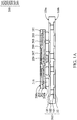
- FIG. 1E is a cross-sectional view of a semiconductor package structure 10a in accordance with some embodiments of the disclosure.
- the semiconductor package structure 10a is a wafer-level semiconductor package structure, for example, a fan-out wafer-level semiconductor package structure.
- the fan-out wafer-level semiconductor package structure may include a flip chip package structure.
- the semiconductor package structure 10a may be mounted on a base (not shown), such as a printed circuit board (PCB), that is formed of polypropylene (PP), polybenzoxazole (PBO) or polyimide.
- the base may be a single layer or a multilayer structure.
- Conductive pads and conductive traces electrically coupled to the conductive pads are typically disposed on the top surface of the base and/or in the base. In this case, the conductive traces may be used for the input/output (I/O) connections of the semiconductor package structure 10a.
- the semiconductor package structure 10a is mounted on the base by a bonding process.
- the first semiconductor package 10a includes bumps 110 that are mounted on and electrically coupled to the base by the bonding process.
- the semiconductor package structure 10a includes a first carrier substrate 100, a second carrier substrate 200 stacked on the first carrier substrate 200 and a semiconductor die 300 mounted on the second carrier substrate 200.
- the first carrier substrate 100 has a first surface 100a and an opposing second surface 100b.
- the second carrier substrate 200 has a first surface 200a and an opposing second surface 200b.
- the second carrier substrate 200 may be stacked on the first carrier substrate 100, so that the second surface 200b of the second carrier substrate 200 faces the first surface 100a of the first carrier substrate 100.
- the semiconductor die 300 is mounted on the first surface 200a of the second carrier substrate 200.
- the first carrier substrate 100 and the second carrier substrate 200 may serve as fan-out layers for the semiconductor die 300 and may also be referred to as package substrate.
- the first carrier substrate 100 is a single layered package substrate and the second carrier substrate 200 is a dual layered package substrate.
- the first carrier substrate 100 may include an insulating layer 102 and conductive traces 101 and 105 that are electrically coupled from each other through conductive vias 103.
- the conductive traces 101 and 105 are respectively disposed on the bottom and top surfaces of the insulating layer 102 (i.e., the second surface 100b and the first surface 100a of the first carrier substrate 100) and the conductive vias 103 are disposed in the insulating layer 102.
- the second carrier substrate 200 may include insulating layers 202 and 204 and conductive traces 201, 205 and 209 that are electrically coupled from each other through conductive vias 203 and 207.
- the conductive traces 201 are disposed on the bottom surface of the insulating layer 202 (i.e., the second surface 200b of the second carrier substrate 200).
- the conductive traces 209 are disposed on the top surface of the insulating layer 204 (i.e., the first surface 200a of the second carrier substrate 200).
- the conductive traces 205 are disposed on the top surface of the insulating layer 202 or the bottom surface of the insulating layer 204.
- conductive vias 203 are disposed in the insulating layer 202 between the conductive traces 201 and 205.
- conductive vias 207 are disposed in the insulating layer 204 between the conductive traces 205 and 209.
- the insulating layers 102, 202 and 204 may be formed of organic materials, which include a polymer base material (e.g., PP, PBO or polyimide), or the like.
- the second carrier substrate 200 is electrically coupled to the first carrier substrate 100 via conductive structures 210 (such as solder balls). Moreover, the second carrier substrate 200 is electrically coupled to the semiconductor die 300 via conductive structures 310 (such as solder bumps).
- the semiconductor die 300 (such as a system-on-chip (SOC) die) may include a logic die including a central processing unit (CPU), a graphics processing unit (GPU), a dynamic random access memory (DRAM) controller or any combination thereof.
- the semiconductor die 300 may include a modem die.
- the semiconductor package structure 10a further includes a heat spreader 415 disposed on the first surface 100a of the first carrier substrate 100 so as to form a cavity therebetween.
- the heat spreader 415 is fixed on the first surface 100a of the first carrier substrate 100 via an adhesive layer 412 (such as a thermal interface adhesive (TIA) layer).
- the heat spreader 415 covers and surrounds the second carrier substrate 200 and the semiconductor die 300 which are in the cavity.
- a thermal interface material (TIM) layer 410 may be adhered between the semiconductor die 300 and the heat spreader 415.
- TIM thermal interface material
- the first semiconductor package of the semiconductor package structure 10a further includes an encapsulating material 420 having a first portion 420a and a second portion 420b.
- the first portion 420a of the encapsulating material 420 may be covered by the heat spreader 415, so that the second carrier substrate 200 and the semiconductor die 300 are surrounded by the first portion 420a of the encapsulating material 420.
- the gap between the semiconductor die 300 and the second carrier substrate 200 and the gap between the second carrier substrate 200 and the first carrier substrate 100 are filled with the first portion 420a of the encapsulating material 420.
- the second portion 420b of the encapsulating material 420 surrounds an exterior sidewall 415a of the heat spreader 415 and exposes a portion of the heat spreader 415 that covers the first portion 420a of the encapsulating material 420 and the semiconductor die 300.
- the formed encapsulating material 420 is merely covered by the heat spreader 415 without surrounding the exterior sidewall 415a of the heat spreader 415.
- the encapsulating material 420 may be a molding compound that is formed of an epoxy, a resin, a moldable polymer, or the like.
- the encapsulating material 420 may be applied while substantially liquid, and then may be cured through a chemical reaction, such as in an epoxy or resin.
- the encapsulating material 420 may be an ultraviolet (UV) or thermally cured polymer applied as a gel or malleable solid capable of being disposed around the heat spreader 415 and in the cavity created by the heat spreader 415 and the first carrier substrate 100, and then may be cured through a UV or thermal curing process.
- the encapsulating material 420 may be cured with a mold (not shown).
- the heat generated from the semiconductor die 300 can also be conducted to the heat spreader 415 through the encapsulating material 420.
- the semiconductor package structure 10a further includes one or more passive devices 220, such as capacitors, mounted on the second surface 200b of the second carrier substrate 200 and directly below the semiconductor die 300.
- passive devices 220 such as capacitors
- the passive device 220 is surrounded and supported by the encapsulating material 420. As a result, the passive device 220 can be prevented from falling off after performing a thermal process, such as a reflow process.
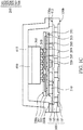
- the passive device 220 may be mounted on the first surface 200a of the second carrier substrate 200 and near the edge of the second carrier substrate 200, as shown in FIG. 1E-1 .
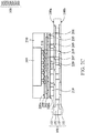
- the passive device 220 is mounted on the first surface 100a of the first carrier substrate 100 and directly below the semiconductor die 300, as shown in FIG. 1E-2 .
- the passive device 220 mounted on the first surface 100a of the first carrier substrate 100 may be near the edge of the first carrier substrate 100.
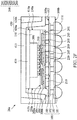
- FIG. 2F is a cross-sectional view of a semiconductor package structure 20a in accordance with some embodiments of the disclosure. Descriptions of elements of the embodiments hereinafter that are the same as or similar to those previously described with reference to FIG. 1E may be omitted for brevity.
- the semiconductor package structure 20a is similar to the semiconductor package structure 10a shown in FIG. 1E .
- the semiconductor package structure 20a includes an encapsulating material 230 disposed on the first surface 200a of the second carrier substrate 200 and surrounding the semiconductor die 300.
- the encapsulating material 230 is surrounded by the first portion 420a of the encapsulating material 420.
- the encapsulating material 230 is surrounded and covered by the hear spreader 415.
- an edge of the TIM layer 410 in the semiconductor package structure 20a is substantially aligned to an edge of the encapsulating material 230.
- the edge of the TIM layer 410 may be substantially aligned to an edge of the semiconductor die 300.
- the passive device 220 may be mounted on the first surface 200a of the second carrier substrate 200 and near the edge of the second carrier substrate 200, as the arrangement of the passive device 220 shown in FIG. 1E-1 . In some other embodiments, the passive device 220 may be mounted on the first surface 100a of the first carrier substrate 100 and directly below the semiconductor die 300, as the arrangement of the passive device 220 shown in FIG. 1E-2 . Alternatively, the passive device 220 mounted on the first surface 100a of the first carrier substrate 100 may be near the edge of the first carrier substrate 100.
- FIG. 3 is a cross-sectional view of a semiconductor package structure 10b in accordance with some embodiments of the disclosure. Descriptions of elements of the embodiments hereinafter that are the same as or similar to those previously described with reference to FIG. 1E may be omitted for brevity.
- the semiconductor package structure 10b is similar to the semiconductor package structure 10a shown in FIG. 1E .
- the semiconductor package structure 10b does not have a TIM layer 410 interposed between the heat spreader 415 and the semiconductor die 300.
- the first portion of encapsulating material 420 is interposed between the heat spreader 415 and the semiconductor die 300 to cover an upper surface of the semiconductor die 300.
- FIG. 4 is a cross-sectional view of a semiconductor package structure 10c in accordance with some embodiments of the disclosure. Descriptions of elements of the embodiments hereinafter that are the same as or similar to those previously described with reference to FIG. 1E may be omitted for brevity.
- the semiconductor package structure 10c is similar to the semiconductor package structure 10a shown in FIG. 1E .
- the semiconductor package structure 10c includes an underfill material layer 430a interposed between the first carrier substrate 100 and the second carrier substrate 200, so that the conductive structures 210 and the passive device 220 are surrounded by the underfill material layer 430a.
- FIG. 5 is a cross-sectional view of a semiconductor package structure 10d in accordance with some embodiments of the disclosure. Descriptions of elements of the embodiments hereinafter that are the same as or similar to those previously described with reference to FIG. 1E may be omitted for brevity.
- the semiconductor package structure 10d is similar to the semiconductor package structure 10a shown in FIG. 1E .
- the semiconductor package structure 10d includes an underfill material layer 430b interposed between the semiconductor die 300 and the second carrier substrate 200, so that the conductive structures 310 are surrounded by the underfill material layer 430b.
- FIG. 6 is a cross-sectional view of a semiconductor package structure 10e in accordance with some embodiments of the disclosure. Descriptions of elements of the embodiments hereinafter that are the same as or similar to those previously described with reference to FIG. 1E may be omitted for brevity.
- the semiconductor package structure 10e is similar to the semiconductor package structure 10a shown in FIG. 1E . As shown in FIG.
- the semiconductor package structure 10e includes an underfill material layer 430a interposed between the first carrier substrate 100 and the second carrier substrate 200 and an underfill material layer 430b interposed between the semiconductor die 300 and the second carrier substrate 200, so that the conductive structures 210 and the passive device 220 are surrounded by the underfill material layer 430b and the conductive structures 310 are surrounded by the underfill material layer 430a.
- FIG. 7 is a cross-sectional view of a semiconductor package structure 10f in accordance with some embodiments of the disclosure. Descriptions of elements of the embodiments hereinafter that are the same as or similar to those previously described with reference to FIG. 6 may be omitted for brevity.
- the semiconductor package structure 10f is similar to the semiconductor package structure 10e shown in FIG. 6 . As shown in FIG. 7 , unlike the semiconductor package structure 10e, the semiconductor package structure 10f does not have an encapsulating material 420. Accordingly, a gap 450 surrounding the TIM layer 410, the semiconductor die 300, the second carrier substrate 200, and the underfill material layers 430a and 430b is formed.
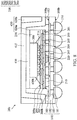
- FIG. 8 is a cross-sectional view of a semiconductor package structure 20b in accordance with some embodiments of the disclosure. Descriptions of elements of the embodiments hereinafter that are the same as or similar to those previously described with reference to FIG. 2F may be omitted for brevity.
- the semiconductor package structure 20b is similar to the semiconductor package structure 20a shown in FIG. 2F .
- the semiconductor package structure 20b includes an underfill material layer 430b interposed between the semiconductor die 300 and the second carrier substrate 200 and surrounded by the encapsulating material 230, so that the conductive structures 310 are surrounded by the underfill material layer 430b.
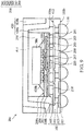
- FIG. 9 is a cross-sectional view of a semiconductor package structure 20c in accordance with some embodiments of the disclosure. Descriptions of elements of the embodiments hereinafter that are the same as or similar to those previously described with reference to FIG. 8 may be omitted for brevity.
- the semiconductor package structure 20c is similar to the semiconductor package structure 20b shown in FIG. 8 . As shown in FIG. 9 , unlike the semiconductor package structure 20b, the semiconductor package structure 20c does not have a TIM layer 410 interposed between the heat spreader 415 and the semiconductor die 300. In the embodiment, the encapsulating material 230 is interposed between the heat spreader 415 and the semiconductor die 300 to cover the upper surface of the semiconductor die 300.
- FIG. 10 is a cross-sectional view of a semiconductor package structure 20d in accordance with some embodiments of the disclosure. Descriptions of elements of the embodiments hereinafter that are the same as or similar to those previously described with reference to FIG. 8 may be omitted for brevity.
- the semiconductor package structure 20d is similar to the semiconductor package structure 20b shown in FIG. 8 .
- the semiconductor package structure 20d includes an underfill material layer 430a interposed between the first carrier substrate 100 and the second carrier substrate 200 and surrounded by the first portion 420a of the encapsulating material 420.
- FIG. 11 is a cross-sectional view of a semiconductor package structure 20e in accordance with some embodiments of the disclosure. Descriptions of elements of the embodiments hereinafter that are the same as or similar to those previously described with reference to FIG. 9 may be omitted for brevity.
- the semiconductor package structure 20e is similar to the semiconductor package structure 20c shown in FIG. 9 .
- the semiconductor package structure 20e includes an underfill material layer 430a interposed between the first carrier substrate 100 and the second carrier substrate 200 and surrounded by the first portion 420a of the encapsulating material 420.
- FIG. 12 is a cross-sectional view of a semiconductor package structure 20f in accordance with some embodiments of the disclosure. Descriptions of elements of the embodiments hereinafter that are the same as or similar to those previously described with reference to FIG. 2F may be omitted for brevity.
- the semiconductor package structure 20f is similar to the semiconductor package structure 20a shown in FIG. 2F .
- the semiconductor package structure 20f includes an underfill material layer 430a interposed between the first carrier substrate 100 and the second carrier substrate 200 and surrounded by the first portion 420a of the encapsulating material 420.
- FIG. 13 is a cross-sectional view of a semiconductor package structure 20g in accordance with some embodiments of the disclosure. Descriptions of elements of the embodiments hereinafter that are the same as or similar to those previously described with reference to FIG. 2F may be omitted for brevity.
- the semiconductor package structure 20g is similar to the semiconductor package structure 20a shown in FIG. 2F .
- the semiconductor package structure 20g includes an underfill material layer 430a interposed between the first carrier substrate 100 and the second carrier substrate 200 and surrounded by the first portion 420a of the encapsulating material 420.
- the semiconductor package structure 20g does not have a TIM layer 410 interposed between the heat spreader 415 and the semiconductor die 300.
- the encapsulating material 230 is interposed between the heat spreader 415 and the semiconductor die 300 to cover the upper surface of the semiconductor die 300.
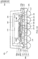
- FIG. 14 is a cross-sectional view of a semiconductor package structure 20h in accordance with some embodiments of the disclosure. Descriptions of elements of the embodiments hereinafter that are the same as or similar to those previously described with reference to FIG. 10 may be omitted for brevity.
- the semiconductor package structure 20h is similar to the semiconductor package structure 20d shown in FIG. 10 . As shown in FIG. 14 , unlike the semiconductor package structure 20d, the semiconductor package structure 20h does not have an encapsulating material 420. Accordingly, a gap 450 surrounding the TIM layer 410, the encapsulating material 230, the second carrier substrate 200, and the underfill material layer 430a is formed.
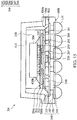
- FIG. 15 is a cross-sectional view of a semiconductor package structure 20i in accordance with some embodiments of the disclosure. Descriptions of elements of the embodiments hereinafter that are the same as or similar to those previously described with reference to FIG. 11 may be omitted for brevity.
- the semiconductor package structure 20i is similar to the semiconductor package structure 20e shown in FIG. 11 . As shown in FIG. 15 , unlike the semiconductor package structure 20e, the semiconductor package structure 20i does not have an encapsulating material 420. Accordingly, a gap 450 surrounding the TIM layer 410, the encapsulating material 230, the second carrier substrate 200, and the underfill material layer 430a is formed.
- FIG. 16 is a cross-sectional view of a semiconductor package structure 20j in accordance with some embodiments of the disclosure. Descriptions of elements of the embodiments hereinafter that are the same as or similar to those previously described with reference to FIG. 12 may be omitted for brevity.
- the semiconductor package structure 20j is similar to the semiconductor package structure 20f shown in FIG. 12 . As shown in FIG. 16 , unlike the semiconductor package structure 20f, the semiconductor package structure 20j does not have an encapsulating material 420. Accordingly, a gap 450 surrounding the TIM layer 410, the encapsulating material 230, the second carrier substrate 200, and the underfill material layer 430a is formed.
- FIG. 17 is a cross-sectional view of a semiconductor package structure 20k in accordance with some embodiments of the disclosure. Descriptions of elements of the embodiments hereinafter that are the same as or similar to those previously described with reference to FIG. 13 may be omitted for brevity.
- the semiconductor package structure 20k is similar to the semiconductor package structure 20g shown in FIG. 13 .
- the semiconductor package structure 20k does not have an encapsulating material 420. Accordingly, a gap 450 surrounding the TIM layer 410, the encapsulating material 230, the second carrier substrate 200, and the underfill material layer 430a is formed.
- FIGS. 1A to 1E are cross-sectional views of various stages of a method for forming a semiconductor package structure 10a, in accordance with some embodiments of the disclosure. Additional operations can be provided before, during, and/or after the stages described in FIGS. 1A to 1E . Some of the stages that are described can be replaced or eliminated for different embodiments. Additional features can be added to the semiconductor package structure 10a. Some of the features described below can be replaced or eliminated for different embodiments.
- a first carrier substrate 100 having a first surface 100a and an opposing second surface 100b and a second carrier substrate 200 having a first surface 200a and an opposing second surface 200b are provided.
- the first carrier substrate 100 is a single layered package substrate and the second carrier substrate 200 is a dual layered package substrate.
- the first carrier substrate 100 may include an insulating layer 102 and conductive traces 101 and 105 that are electrically coupled from each other through conductive vias 103.
- the conductive traces 101 and 105 are respectively disposed on the bottom and top surfaces of the insulating layer 102 (i.e., the second surface 100b and the first surface 100a of the first carrier substrate 100) and the conductive vias 103 are disposed in the insulating layer 102.
- the second carrier substrate 200 may include insulating layers 202 and 204 and conductive traces 201, 205 and 209 that are electrically coupled from each other through conductive vias 203 and 207.
- the conductive traces 201 are disposed on the bottom surface of the insulating layer 202 (i.e., the second surface 200b of the second carrier substrate 200).
- the conductive traces 209 are disposed on the top surface of the insulating layer 204 (i.e., the first surface 200a of the second carrier substrate 200).
- the conductive traces 205 are disposed on the top surface of the insulating layer 202 or the bottom surface of the insulating layer 204.
- conductive vias 203 are disposed in the insulating layer 202 between the conductive traces 201 and 205.
- conductive vias 207 are disposed in the insulating layer 204 between the conductive traces 205 and 209.
- conductive structures 210 such as solder balls
- at least one passive device 220 is mounted on the second surface 200b of the carrier substrate 200.
- the passive device 220 may be mounted on the first surface 200b of the second carrier substrate 200 or the first surface 100a of the first carrier substrate 100.
- the second carrier substrate 200 is stacked on the first carrier substrate 100, so that the second surface 200b of the second carrier substrate 200 faces the first surface 100a of the first carrier substrate 100 and is electrically coupled to the first carrier substrate 100 via conductive structures 210.
- a semiconductor die 300 is provided.
- the semiconductor die 300 (such as a system-on-chip (SOC) die) may include a logic die including a CPU, a GPU, a DRAM controller or any combination thereof.
- the semiconductor die 300 may include a modem die.
- the semiconductor die 300 is stacked on the first surface 200a of the second carrier substrate 200, so that the second carrier substrate 200 is electrically coupled to the semiconductor die 300 via conductive structures 310 (such as solder bumps).
- a reflow process may be performed, so that the second carrier substrate 200 is mounted onto the first carrier substrate 100 through the conductive structures 210 and the semiconductor die 300 is mounted onto the second carrier substrate 200 through the conductive structures 310.
- an optional TIM layer 410 may be formed on the semiconductor die 300 and an adhesive layer 412 (such as a TIA layer) may be formed on the first surface 100a of the first carrier substrate 100 via by respective dispensing processes.
- a heat spreader 415 is formed on the TIM layer 410 and the first surface 100a of the first carrier substrate 100 so as to form a cavity between the heat spreader 415 and the first carrier substrate 100.
- a curing process is performed on the TIM layer 410 and the adhesive layer 412, so that the heat spreader 415 is fixed on the first surface 100a of the first carrier substrate 100 via the adhesive layer 412 and adhered to the semiconductor die 300 via the TIM layer 410.
- the second carrier substrate 200 and the semiconductor die 300 which are in the cavity, so that the heat spreader 415 covers and surrounds second carrier substrate 200 and the semiconductor die 300.
- an encapsulating material 420 such as a molding compound, is formed on the first carrier substrate 100.
- the encapsulating material 420 has a first portion 420a and a second portion 420b.
- the first portion 420a of the encapsulating material 420 may be in the cavity created by the heat spreader 415 and the first carrier substrate 100, so that the first portion 420a of the encapsulating material 420 is covered by the heat spreader 415, and the second carrier substrate 200 and the semiconductor die 300 are surrounded by the first portion 420a of the encapsulating material 420.
- the gap between the semiconductor die 300 and the second carrier substrate 200 and the gap between the second carrier substrate 200 and the first carrier substrate 100 are filled with the first portion 420a of the encapsulating material 420.
- the second portion 420b of the encapsulating material 420 surrounds an exterior sidewall 415a of the heat spreader 415 and exposes a portion of the heat spreader 415 that covers the first portion 420a of the encapsulating material 420 and the semiconductor die 300.
- the encapsulating material 420 is merely covered by the heat spreader 415 without surrounding the exterior sidewall 415a of the heat spreader 415
- bumps 110 are formed on the second surface 100b of the first carrier substrate 100 so as to complete the fabrication of the semiconductor package structure 10a.
- FIGS. 2A to 2F are cross-sectional views of various stages of a method for forming a semiconductor package structure 20a, in accordance with some embodiments of the disclosure. Descriptions of elements of the embodiments hereinafter that are the same as or similar to those previously described with reference to FIGS. 1A to 1E may be omitted for brevity. Additional operations can be provided before, during, and/or after the stages described in FIGS. 2A to 2F . Some of the stages that are described can be replaced or eliminated for different embodiments. Additional features can be added to the semiconductor package structure 20a. Some of the features described below can be replaced or eliminated for different embodiments.
- a second carrier substrate 200 having a first surface 200a and an opposing second surface 200b and a semiconductor die 300 are provided.
- the semiconductor die 300 is stacked on the first surface 200a of the second carrier substrate 200, so that the second carrier substrate 200 is electrically coupled to the semiconductor die 300 via conductive structures 310 (such as solder bumps).
- conductive structures 310 such as solder bumps.
- a reflow process may be performed, so that the semiconductor die 300 is mounted onto the second carrier substrate 200 through the conductive structures 310.
- an encapsulating material 230 such as a molding compound, is formed on the first surface 200a of the second carrier substrate 200 to surround the semiconductor die 300 and expose the upper surface of the semiconductor die 300. Also, the gap between the semiconductor die 300 and the second carrier substrate 200 is filled with the encapsulating material 230. Afterwards, conductive structures 210 (such as solder balls) and at least one passive device 220 (such as a capacitor) is mounted on the second surface 200b of the carrier substrate 200. In some other embodiments, the passive device 220 may be mounted on the first surface 200b of the second carrier substrate 200.
- a first carrier substrate 100 having a first surface 100a and an opposing second surface 100b is provided.
- the second carrier substrate 200 with the semiconductor die 300 and the encapsulating material 230 is stacked on the first surface 100a of the first carrier substrate 100.
- a reflow process may be performed, so that the second carrier substrate 200 with the semiconductor die 300 and the encapsulating material 230 is mounted onto the first carrier substrate 100 through the conductive structures 210.
- an optional TIM layer 410 may be formed on the semiconductor die 300 and the encapsulating material 230 and an adhesive layer 412 (such as a TIA layer) may be formed on the first surface 100a of the first carrier substrate 100 via by respective dispensing processes.
- an edge 400a of the TIM layer 410 is substantially aligned to an edge 230a of the encapsulating material 230.
- a heat spreader 415 is formed on the TIM layer 410 and the first surface 100a of the first carrier substrate 100 so as to form a cavity between the heat spreader 415 and the first carrier substrate 100.
- a curing process is performed on the TIM layer 410 and the adhesive layer 412, so that the heat spreader 415 is fixed on the first surface 100a of the first carrier substrate 100 via the adhesive layer 412 and adhered to the semiconductor die 300 and the encapsulating material 230 via the TIM layer 410.
- the second carrier substrate 200 and the semiconductor die 300 which are in the cavity, so as to be covered and surrounded by the heat spreader 415.
- an encapsulating material 420 such as a molding compound, is formed on the first carrier substrate 100.
- the passive device 220 is not mounted on the second carrier substrate 200 and may be mounted on the first surface 100a of the first carrier substrate 100 prior to formation of the encapsulating material 420.
- the encapsulating material 420 has a first portion 420a and a second portion 420b.
- the first portion 420a of the encapsulating material 420 is covered by the heat spreader 415, and the second carrier substrate 200 and the encapsulating material 230 are surrounded by the first portion 420a of the encapsulating material 420.
- the gap between the second carrier substrate 200 and the first carrier substrate 100 is filled with the first portion 420a of the encapsulating material 420.
- the second portion 420b of the encapsulating material 420 surrounds an exterior sidewall 415a of the heat spreader 415 and exposes a portion of the heat spreader 415 that covers the first portion 420a of the 420, the encapsulating material 230 and the semiconductor die 300.
- the encapsulating material 420 is merely covered by the heat spreader 415 without surrounding the exterior sidewall 415a of the heat spreader 415.
- bumps 110 are formed on the second surface 100b of the first carrier substrate 100 so as to complete the fabrication of the semiconductor package structure 20a.
- the semiconductor package structures 10b to 10f respectively shown in FIGS. 3 to 7 and the semiconductor package structures 20b to 20k respectively shown in FIGS. 8 to 17 may be fabricated by the method same as or similar to the method for forming the semiconductor package structure 10a or the method for forming the semiconductor package structure 10a.
- the semiconductor package structure utilizes a combination of first and second carrier substrates (i.e., package substrates) as a fan-out layer for a semiconductor die in the semiconductor package structure, compared to a conventional semiconductor package structure that merely utilizes a single package substrate with a complicated multilayer interconnect structure therein as a fan-out layer, the number of interconnect layers in the package substrates and the entire thickness of the package substrates can be reduced, so as to simplify the semiconductor package structure and reduce the manufacturing cost of the semiconductor package structure.
- first and second carrier substrates i.e., package substrates
- the encapsulating material that surrounds the semiconductor die and be covered by the heat spreader can provide vertical and lateral paths for heat dissipation. As a result, the reliability of the semiconductor package structure can be increased. Moreover, since the encapsulating material is formed on the first carrier substrate and encapsulates the second carrier substrate, warpage of the semiconductor package structure can be mitigated or improved.
- the passive device can be mounted on the upper surface of the first carrier substrate, the upper surface of the second carrier substrate, or the lower surface of the second carrier substrate, the design flexibility for conductive structures (e.g., solder balls) between the first and second carrier substrates can be increased. Moreover, in the case of the passive device mounted on the lower surface of the second carrier substrate, the passive device can be protected and supported by the encapsulating material. As a result, the passive device can be prevented from falling off, thereby addressing the rework issue for the passive device or the second carrier substrate.
- conductive structures e.g., solder balls
Landscapes
- Structures Or Materials For Encapsulating Or Coating Semiconductor Devices Or Solid State Devices (AREA)
- Wire Bonding (AREA)
Abstract
Description
- This application claims the benefit of U.S. Provisional Application No.
62/396,906 - The present invention relates to a semiconductor package structure, and in particular to a highly cost-effective fan-out package structure and a method for forming the same.
- In the semiconductor packaging industry, there is a demand for reducing the manufacturing cost of semiconductor packages. To accomplish this, various package structure designs have been developed. One of the package structure designs currently in use is the flip-chip package structure. The adoption of a flip chip package structure in many applications is driven by performance needs and the ability to achieve a smaller die with a flip chip design.
- In a flip-chip package structure, a semiconductor die (also referred to as an integrated circuit (IC) chip or "chip") that is formed with solder bumps is typically bonded directly to metal pads of a package substrate. Such solder bumps are affixed to I/O bonding pads of the semiconductor die. During packaging, the semiconductor die is "flipped" so that the solder bumps form electrical interconnections between the semiconductor die and the packaging substrate.
- In order to ensure miniaturization and multi-functionality of electronic products, it is desired that semiconductor packages are small in size, operate at high speeds, and have high functionality. Accordingly, the semiconductor die utilizes the package substrate to serve as a fan-out layer.
- However, in order to respond to the increase in I/O pads, a complicated multilayer interconnect structure is formed in the package substrate. As a result, the manufacturing cost of the package substrate is greatly increased, while the yield of the package substrate is reduced. These cause reductions in the reliability, yield, and throughput of the semiconductor package structure, while the manufacturing cost of the semiconductor package structure goes up.
- Thus, a novel semiconductor package structure is desirable.
- Semiconductor package structures and methods for forming the same are provided. An exemplary embodiment of a semiconductor package structure includes a first carrier substrate having a first surface and an opposing second surface. A second carrier substrate is stacked on the first carrier substrate and has a first surface and an opposing second surface that faces the first surface of the first carrier substrate. A semiconductor die is mounted on the first surface of the second carrier substrate. A heat spreader is disposed on the first surface of the first carrier substrate to cover and surround the second carrier substrate and the semiconductor die.
- Another exemplary embodiment of a semiconductor package structure includes a first carrier substrate having a first surface and an opposing second surface. A second carrier substrate is stacked on the first carrier substrate and has a first surface and an opposing second surface that faces the first surface of the first carrier substrate. A semiconductor die is mounted on the first surface of the second carrier substrate. A first encapsulating material is disposed on the first surface of the second carrier substrate and surrounds the semiconductor die. A heat spreader is disposed on the first surface of the first carrier substrate to cover and surround the second carrier substrate and the first encapsulating material.
- An exemplary embodiment of a method for forming a semiconductor package structure includes providing a first carrier substrate having a first surface and an opposing second surface and a second carrier substrate having a first surface and an opposing second surface. The second carrier substrate is stacked on the first carrier substrate. The second surface of the second carrier substrate faces the first surface of the first carrier substrate. A semiconductor die is stacked on the first surface of the second carrier substrate. A heat spreader is formed on the first surface of the first carrier substrate to cover and surround the second carrier substrate and the semiconductor die.
- Another exemplary embodiment of a method for forming a semiconductor package structure includes providing a second carrier substrate having a first surface and an opposing second surface. A semiconductor die is mounted on the first surface of the second carrier substrate. A first encapsulating material is formed on the first surface of the second carrier substrate to surround the semiconductor die. A first carrier substrate having a first surface and an opposing second surface is provided. The second carrier substrate with the semiconductor die and the first encapsulating material is mounted on the first surface of the first carrier substrate. A heat spreader id formed on the first surface of the first carrier substrate to cover and surround the second carrier substrate and the first encapsulating material.
- A detailed description is given in the following embodiments with reference to the accompanying drawings.
- The present invention can be more fully understood by reading the subsequent detailed description and examples with references made to the accompanying drawings, wherein:
-
FIGS. 1A to 1E are cross-sectional views of various stages of a method for forming a semiconductor package structure, in accordance with some embodiments of the disclosure. -
FIG. 1E-1 is a cross-sectional view of a semiconductor package structure in accordance with some embodiments of the disclosure. -
FIG. 1E-2 is a cross-sectional view of a semiconductor package structure in accordance with some embodiments of the disclosure -
FIGS. 2A to 2F are cross-sectional views of various stages of a method for forming a semiconductor package structure, in accordance with some embodiments of the disclosure. -
FIG. 3 is a cross-sectional view of a semiconductor package structure in accordance with some embodiments of the disclosure. -
FIG. 4 is a cross-sectional view of a semiconductor package structure in accordance with some embodiments of the disclosure. -
FIG. 5 is a cross-sectional view of a semiconductor package structure in accordance with some embodiments of the disclosure. -
FIG. 6 is a cross-sectional view of a semiconductor package structure in accordance with some embodiments of the disclosure. -
FIG. 7 is a cross-sectional view of a semiconductor package structure in accordance with some embodiments of the disclosure. -
FIG. 8 is a cross-sectional view of a semiconductor package structure in accordance with some embodiments of the disclosure. -
FIG. 9 is a cross-sectional view of a semiconductor package structure in accordance with some embodiments of the disclosure. -
FIG. 10 is a cross-sectional view of a semiconductor package structure in accordance with some embodiments of the disclosure. -
FIG. 11 is a cross-sectional view of a semiconductor package structure in accordance with some embodiments of the disclosure. -
FIG. 12 is a cross-sectional view of a semiconductor package structure in accordance with some embodiments of the disclosure. -
FIG. 13 is a cross-sectional view of a semiconductor package structure in accordance with some embodiments of the disclosure. -
FIG. 14 is a cross-sectional view of a semiconductor package structure in accordance with some embodiments of the disclosure. -
FIG. 15 is a cross-sectional view of a semiconductor package structure in accordance with some embodiments of the disclosure. -
FIG. 16 is a cross-sectional view of a semiconductor package structure in accordance with some embodiments of the disclosure. -
FIG. 17 is a cross-sectional view of a semiconductor package structure in accordance with some embodiments of the disclosure. - The following description is of the best-contemplated mode of carrying out the invention. This description is made for the purpose of illustrating the general principles of the invention and should not be taken in a limiting sense. The scope of the invention is determined by reference to the appended claims.
- The present invention will be described with respect to particular embodiments and with reference to certain drawings, but the invention is not limited thereto and is only limited by the claims. The drawings described are only schematic and are non-limiting. In the drawings, the size of some of the elements may be exaggerated for illustrative purposes and not drawn to scale. The dimensions and the relative dimensions do not correspond to actual dimensions in the practice of the invention.
-
FIG. 1E is a cross-sectional view of asemiconductor package structure 10a in accordance with some embodiments of the disclosure. In some embodiments, thesemiconductor package structure 10a is a wafer-level semiconductor package structure, for example, a fan-out wafer-level semiconductor package structure. In one embodiment, the fan-out wafer-level semiconductor package structure may include a flip chip package structure. - Referring to
FIG. 1E , thesemiconductor package structure 10a may be mounted on a base (not shown), such as a printed circuit board (PCB), that is formed of polypropylene (PP), polybenzoxazole (PBO) or polyimide. In some embodiments, the base may be a single layer or a multilayer structure. Conductive pads and conductive traces electrically coupled to the conductive pads are typically disposed on the top surface of the base and/or in the base. In this case, the conductive traces may be used for the input/output (I/O) connections of thesemiconductor package structure 10a. In some embodiments, thesemiconductor package structure 10a is mounted on the base by a bonding process. For example, thefirst semiconductor package 10a includesbumps 110 that are mounted on and electrically coupled to the base by the bonding process. - In some embodiments, the
semiconductor package structure 10a includes afirst carrier substrate 100, asecond carrier substrate 200 stacked on thefirst carrier substrate 200 and asemiconductor die 300 mounted on thesecond carrier substrate 200. For example, thefirst carrier substrate 100 has afirst surface 100a and an opposingsecond surface 100b. Moreover, thesecond carrier substrate 200 has afirst surface 200a and an opposingsecond surface 200b. Thesecond carrier substrate 200 may be stacked on thefirst carrier substrate 100, so that thesecond surface 200b of thesecond carrier substrate 200 faces thefirst surface 100a of thefirst carrier substrate 100. Moreover, the semiconductor die 300 is mounted on thefirst surface 200a of thesecond carrier substrate 200. - The
first carrier substrate 100 and thesecond carrier substrate 200 may serve as fan-out layers for the semiconductor die 300 and may also be referred to as package substrate. In some embodiments, thefirst carrier substrate 100 is a single layered package substrate and thesecond carrier substrate 200 is a dual layered package substrate. In those cases, thefirst carrier substrate 100 may include an insulatinglayer 102 andconductive traces conductive vias 103. The conductive traces 101 and 105 are respectively disposed on the bottom and top surfaces of the insulating layer 102 (i.e., thesecond surface 100b and thefirst surface 100a of the first carrier substrate 100) and theconductive vias 103 are disposed in the insulatinglayer 102. Moreover, thesecond carrier substrate 200 may include insulatinglayers conductive traces conductive vias conductive traces 201 are disposed on the bottom surface of the insulating layer 202 (i.e., thesecond surface 200b of the second carrier substrate 200). The conductive traces 209 are disposed on the top surface of the insulating layer 204 (i.e., thefirst surface 200a of the second carrier substrate 200). The conductive traces 205 are disposed on the top surface of the insulatinglayer 202 or the bottom surface of the insulatinglayer 204. Moreover,conductive vias 203 are disposed in the insulatinglayer 202 between theconductive traces conductive vias 207 are disposed in the insulatinglayer 204 between theconductive traces layers - In some embodiments, the
second carrier substrate 200 is electrically coupled to thefirst carrier substrate 100 via conductive structures 210 (such as solder balls). Moreover, thesecond carrier substrate 200 is electrically coupled to the semiconductor die 300 via conductive structures 310 (such as solder bumps). - In some embodiments, the semiconductor die 300 (such as a system-on-chip (SOC) die) may include a logic die including a central processing unit (CPU), a graphics processing unit (GPU), a dynamic random access memory (DRAM) controller or any combination thereof. Alternatively, the semiconductor die 300 may include a modem die.
- In some embodiments, the
semiconductor package structure 10a further includes aheat spreader 415 disposed on thefirst surface 100a of thefirst carrier substrate 100 so as to form a cavity therebetween. For example, theheat spreader 415 is fixed on thefirst surface 100a of thefirst carrier substrate 100 via an adhesive layer 412 (such as a thermal interface adhesive (TIA) layer). Theheat spreader 415 covers and surrounds thesecond carrier substrate 200 and the semiconductor die 300 which are in the cavity. Moreover, a thermal interface material (TIM)layer 410 may be adhered between the semiconductor die 300 and theheat spreader 415. As a result, the heat generated from the semiconductor die 300 can be conducted to theheat spreader 415 through theTIM layer 410 and through thesecond carrier substrate 200, thefirst carrier substrate 100 and theadhesive layer 412. - In some embodiments, the first semiconductor package of the
semiconductor package structure 10a further includes an encapsulatingmaterial 420 having afirst portion 420a and asecond portion 420b. Thefirst portion 420a of the encapsulatingmaterial 420 may be covered by theheat spreader 415, so that thesecond carrier substrate 200 and the semiconductor die 300 are surrounded by thefirst portion 420a of the encapsulatingmaterial 420. Also, the gap between the semiconductor die 300 and thesecond carrier substrate 200 and the gap between thesecond carrier substrate 200 and thefirst carrier substrate 100 are filled with thefirst portion 420a of the encapsulatingmaterial 420. Moreover, thesecond portion 420b of the encapsulatingmaterial 420 surrounds anexterior sidewall 415a of theheat spreader 415 and exposes a portion of theheat spreader 415 that covers thefirst portion 420a of the encapsulatingmaterial 420 and the semiconductor die 300. Alternatively, the formed encapsulatingmaterial 420 is merely covered by theheat spreader 415 without surrounding theexterior sidewall 415a of theheat spreader 415. - In some embodiments, the encapsulating
material 420 may be a molding compound that is formed of an epoxy, a resin, a moldable polymer, or the like. The encapsulatingmaterial 420 may be applied while substantially liquid, and then may be cured through a chemical reaction, such as in an epoxy or resin. In some other embodiments, the encapsulatingmaterial 420 may be an ultraviolet (UV) or thermally cured polymer applied as a gel or malleable solid capable of being disposed around theheat spreader 415 and in the cavity created by theheat spreader 415 and thefirst carrier substrate 100, and then may be cured through a UV or thermal curing process. The encapsulatingmaterial 420 may be cured with a mold (not shown). In some embodiments, the heat generated from the semiconductor die 300 can also be conducted to theheat spreader 415 through the encapsulatingmaterial 420. - In some embodiments, the
semiconductor package structure 10a further includes one or morepassive devices 220, such as capacitors, mounted on thesecond surface 200b of thesecond carrier substrate 200 and directly below the semiconductor die 300. In order to simplify the diagram, only one passive device is depicted. Thepassive device 220 is surrounded and supported by the encapsulatingmaterial 420. As a result, thepassive device 220 can be prevented from falling off after performing a thermal process, such as a reflow process. - Alternatively, the
passive device 220 may be mounted on thefirst surface 200a of thesecond carrier substrate 200 and near the edge of thesecond carrier substrate 200, as shown inFIG. 1E-1 . In some other embodiments, thepassive device 220 is mounted on thefirst surface 100a of thefirst carrier substrate 100 and directly below the semiconductor die 300, as shown inFIG. 1E-2 . Alternatively, thepassive device 220 mounted on thefirst surface 100a of thefirst carrier substrate 100 may be near the edge of thefirst carrier substrate 100. -
FIG. 2F is a cross-sectional view of asemiconductor package structure 20a in accordance with some embodiments of the disclosure. Descriptions of elements of the embodiments hereinafter that are the same as or similar to those previously described with reference toFIG. 1E may be omitted for brevity. In the embodiment, thesemiconductor package structure 20a is similar to thesemiconductor package structure 10a shown inFIG. 1E . As shown inFIG. 2F , unlike thesemiconductor package structure 10a, thesemiconductor package structure 20a includes an encapsulatingmaterial 230 disposed on thefirst surface 200a of thesecond carrier substrate 200 and surrounding the semiconductor die 300. The encapsulatingmaterial 230 is surrounded by thefirst portion 420a of the encapsulatingmaterial 420. Also, the encapsulatingmaterial 230 is surrounded and covered by the hearspreader 415. - Moreover, unlike the
semiconductor package structure 10a, an edge of theTIM layer 410 in thesemiconductor package structure 20a is substantially aligned to an edge of the encapsulatingmaterial 230. Alternatively, the edge of theTIM layer 410 may be substantially aligned to an edge of the semiconductor die 300. - In some embodiments, the
passive device 220 may be mounted on thefirst surface 200a of thesecond carrier substrate 200 and near the edge of thesecond carrier substrate 200, as the arrangement of thepassive device 220 shown inFIG. 1E-1 . In some other embodiments, thepassive device 220 may be mounted on thefirst surface 100a of thefirst carrier substrate 100 and directly below the semiconductor die 300, as the arrangement of thepassive device 220 shown inFIG. 1E-2 . Alternatively, thepassive device 220 mounted on thefirst surface 100a of thefirst carrier substrate 100 may be near the edge of thefirst carrier substrate 100. -
FIG. 3 is a cross-sectional view of asemiconductor package structure 10b in accordance with some embodiments of the disclosure. Descriptions of elements of the embodiments hereinafter that are the same as or similar to those previously described with reference toFIG. 1E may be omitted for brevity. In the embodiment, thesemiconductor package structure 10b is similar to thesemiconductor package structure 10a shown inFIG. 1E . As shown inFIG. 3 , unlike thesemiconductor package structure 10a, thesemiconductor package structure 10b does not have aTIM layer 410 interposed between theheat spreader 415 and the semiconductor die 300. In the embodiment, the first portion of encapsulatingmaterial 420 is interposed between theheat spreader 415 and the semiconductor die 300 to cover an upper surface of the semiconductor die 300. -
FIG. 4 is a cross-sectional view of asemiconductor package structure 10c in accordance with some embodiments of the disclosure. Descriptions of elements of the embodiments hereinafter that are the same as or similar to those previously described with reference toFIG. 1E may be omitted for brevity. In the embodiment, thesemiconductor package structure 10c is similar to thesemiconductor package structure 10a shown inFIG. 1E . As shown inFIG. 4 , unlike thesemiconductor package structure 10a, thesemiconductor package structure 10c includes anunderfill material layer 430a interposed between thefirst carrier substrate 100 and thesecond carrier substrate 200, so that theconductive structures 210 and thepassive device 220 are surrounded by theunderfill material layer 430a. -
FIG. 5 is a cross-sectional view of asemiconductor package structure 10d in accordance with some embodiments of the disclosure. Descriptions of elements of the embodiments hereinafter that are the same as or similar to those previously described with reference toFIG. 1E may be omitted for brevity. In the embodiment, thesemiconductor package structure 10d is similar to thesemiconductor package structure 10a shown inFIG. 1E . As shown inFIG. 5 , unlike thesemiconductor package structure 10a, thesemiconductor package structure 10d includes anunderfill material layer 430b interposed between the semiconductor die 300 and thesecond carrier substrate 200, so that theconductive structures 310 are surrounded by theunderfill material layer 430b. -
FIG. 6 is a cross-sectional view of asemiconductor package structure 10e in accordance with some embodiments of the disclosure. Descriptions of elements of the embodiments hereinafter that are the same as or similar to those previously described with reference toFIG. 1E may be omitted for brevity. In the embodiment, thesemiconductor package structure 10e is similar to thesemiconductor package structure 10a shown inFIG. 1E . As shown inFIG. 6 , unlike thesemiconductor package structure 10a, thesemiconductor package structure 10e includes anunderfill material layer 430a interposed between thefirst carrier substrate 100 and thesecond carrier substrate 200 and anunderfill material layer 430b interposed between the semiconductor die 300 and thesecond carrier substrate 200, so that theconductive structures 210 and thepassive device 220 are surrounded by theunderfill material layer 430b and theconductive structures 310 are surrounded by theunderfill material layer 430a. -
FIG. 7 is a cross-sectional view of asemiconductor package structure 10f in accordance with some embodiments of the disclosure. Descriptions of elements of the embodiments hereinafter that are the same as or similar to those previously described with reference toFIG. 6 may be omitted for brevity. In the embodiment, thesemiconductor package structure 10f is similar to thesemiconductor package structure 10e shown inFIG. 6 . As shown inFIG. 7 , unlike thesemiconductor package structure 10e, thesemiconductor package structure 10f does not have an encapsulatingmaterial 420. Accordingly, agap 450 surrounding theTIM layer 410, the semiconductor die 300, thesecond carrier substrate 200, and theunderfill material layers -
FIG. 8 is a cross-sectional view of asemiconductor package structure 20b in accordance with some embodiments of the disclosure. Descriptions of elements of the embodiments hereinafter that are the same as or similar to those previously described with reference toFIG. 2F may be omitted for brevity. In the embodiment, thesemiconductor package structure 20b is similar to thesemiconductor package structure 20a shown inFIG. 2F . As shown inFIG. 8 , unlike thesemiconductor package structure 20a, thesemiconductor package structure 20b includes anunderfill material layer 430b interposed between the semiconductor die 300 and thesecond carrier substrate 200 and surrounded by the encapsulatingmaterial 230, so that theconductive structures 310 are surrounded by theunderfill material layer 430b. -
FIG. 9 is a cross-sectional view of asemiconductor package structure 20c in accordance with some embodiments of the disclosure. Descriptions of elements of the embodiments hereinafter that are the same as or similar to those previously described with reference toFIG. 8 may be omitted for brevity. In the embodiment, thesemiconductor package structure 20c is similar to thesemiconductor package structure 20b shown inFIG. 8 . As shown inFIG. 9 , unlike thesemiconductor package structure 20b, thesemiconductor package structure 20c does not have aTIM layer 410 interposed between theheat spreader 415 and the semiconductor die 300. In the embodiment, the encapsulatingmaterial 230 is interposed between theheat spreader 415 and the semiconductor die 300 to cover the upper surface of the semiconductor die 300. -
FIG. 10 is a cross-sectional view of asemiconductor package structure 20d in accordance with some embodiments of the disclosure. Descriptions of elements of the embodiments hereinafter that are the same as or similar to those previously described with reference toFIG. 8 may be omitted for brevity. In the embodiment, thesemiconductor package structure 20d is similar to thesemiconductor package structure 20b shown inFIG. 8 . As shown inFIG. 10 , unlike thesemiconductor package structure 20b, thesemiconductor package structure 20d includes anunderfill material layer 430a interposed between thefirst carrier substrate 100 and thesecond carrier substrate 200 and surrounded by thefirst portion 420a of the encapsulatingmaterial 420. -
FIG. 11 is a cross-sectional view of asemiconductor package structure 20e in accordance with some embodiments of the disclosure. Descriptions of elements of the embodiments hereinafter that are the same as or similar to those previously described with reference toFIG. 9 may be omitted for brevity. In the embodiment, thesemiconductor package structure 20e is similar to thesemiconductor package structure 20c shown inFIG. 9 . As shown inFIG. 11 , unlike thesemiconductor package structure 20c, thesemiconductor package structure 20e includes anunderfill material layer 430a interposed between thefirst carrier substrate 100 and thesecond carrier substrate 200 and surrounded by thefirst portion 420a of the encapsulatingmaterial 420. -
FIG. 12 is a cross-sectional view of asemiconductor package structure 20f in accordance with some embodiments of the disclosure. Descriptions of elements of the embodiments hereinafter that are the same as or similar to those previously described with reference toFIG. 2F may be omitted for brevity. In the embodiment, thesemiconductor package structure 20f is similar to thesemiconductor package structure 20a shown inFIG. 2F . As shown inFIG. 12 , unlike thesemiconductor package structure 20a, thesemiconductor package structure 20f includes anunderfill material layer 430a interposed between thefirst carrier substrate 100 and thesecond carrier substrate 200 and surrounded by thefirst portion 420a of the encapsulatingmaterial 420. -
FIG. 13 is a cross-sectional view of asemiconductor package structure 20g in accordance with some embodiments of the disclosure. Descriptions of elements of the embodiments hereinafter that are the same as or similar to those previously described with reference toFIG. 2F may be omitted for brevity. In the embodiment, thesemiconductor package structure 20g is similar to thesemiconductor package structure 20a shown inFIG. 2F . As shown inFIG. 13 , unlike thesemiconductor package structure 20a, thesemiconductor package structure 20g includes anunderfill material layer 430a interposed between thefirst carrier substrate 100 and thesecond carrier substrate 200 and surrounded by thefirst portion 420a of the encapsulatingmaterial 420. Moreover, thesemiconductor package structure 20g does not have aTIM layer 410 interposed between theheat spreader 415 and the semiconductor die 300. In the embodiment, the encapsulatingmaterial 230 is interposed between theheat spreader 415 and the semiconductor die 300 to cover the upper surface of the semiconductor die 300. -
FIG. 14 is a cross-sectional view of asemiconductor package structure 20h in accordance with some embodiments of the disclosure. Descriptions of elements of the embodiments hereinafter that are the same as or similar to those previously described with reference toFIG. 10 may be omitted for brevity. In the embodiment, thesemiconductor package structure 20h is similar to thesemiconductor package structure 20d shown inFIG. 10 . As shown inFIG. 14 , unlike thesemiconductor package structure 20d, thesemiconductor package structure 20h does not have an encapsulatingmaterial 420. Accordingly, agap 450 surrounding theTIM layer 410, the encapsulatingmaterial 230, thesecond carrier substrate 200, and theunderfill material layer 430a is formed. -
FIG. 15 is a cross-sectional view of asemiconductor package structure 20i in accordance with some embodiments of the disclosure. Descriptions of elements of the embodiments hereinafter that are the same as or similar to those previously described with reference toFIG. 11 may be omitted for brevity. In the embodiment, thesemiconductor package structure 20i is similar to thesemiconductor package structure 20e shown inFIG. 11 . As shown inFIG. 15 , unlike thesemiconductor package structure 20e, thesemiconductor package structure 20i does not have an encapsulatingmaterial 420. Accordingly, agap 450 surrounding theTIM layer 410, the encapsulatingmaterial 230, thesecond carrier substrate 200, and theunderfill material layer 430a is formed. -
FIG. 16 is a cross-sectional view of asemiconductor package structure 20j in accordance with some embodiments of the disclosure. Descriptions of elements of the embodiments hereinafter that are the same as or similar to those previously described with reference toFIG. 12 may be omitted for brevity. In the embodiment, thesemiconductor package structure 20j is similar to thesemiconductor package structure 20f shown inFIG. 12 . As shown inFIG. 16 , unlike thesemiconductor package structure 20f, thesemiconductor package structure 20j does not have an encapsulatingmaterial 420. Accordingly, agap 450 surrounding theTIM layer 410, the encapsulatingmaterial 230, thesecond carrier substrate 200, and theunderfill material layer 430a is formed. -
FIG. 17 is a cross-sectional view of asemiconductor package structure 20k in accordance with some embodiments of the disclosure. Descriptions of elements of the embodiments hereinafter that are the same as or similar to those previously described with reference toFIG. 13 may be omitted for brevity. In the embodiment, thesemiconductor package structure 20k is similar to thesemiconductor package structure 20g shown inFIG. 13 . As shown inFIG. 17 , unlike thesemiconductor package structure 20g, thesemiconductor package structure 20k does not have an encapsulatingmaterial 420. Accordingly, agap 450 surrounding theTIM layer 410, the encapsulatingmaterial 230, thesecond carrier substrate 200, and theunderfill material layer 430a is formed. -
FIGS. 1A to 1E are cross-sectional views of various stages of a method for forming asemiconductor package structure 10a, in accordance with some embodiments of the disclosure. Additional operations can be provided before, during, and/or after the stages described inFIGS. 1A to 1E . Some of the stages that are described can be replaced or eliminated for different embodiments. Additional features can be added to thesemiconductor package structure 10a. Some of the features described below can be replaced or eliminated for different embodiments. - As shown in
FIG. 1A , afirst carrier substrate 100 having afirst surface 100a and an opposingsecond surface 100b and asecond carrier substrate 200 having afirst surface 200a and an opposingsecond surface 200b are provided. In some embodiments, thefirst carrier substrate 100 is a single layered package substrate and thesecond carrier substrate 200 is a dual layered package substrate. In those cases, thefirst carrier substrate 100 may include an insulatinglayer 102 andconductive traces conductive vias 103. The conductive traces 101 and 105 are respectively disposed on the bottom and top surfaces of the insulating layer 102 (i.e., thesecond surface 100b and thefirst surface 100a of the first carrier substrate 100) and theconductive vias 103 are disposed in the insulatinglayer 102. - Moreover, the
second carrier substrate 200 may include insulatinglayers conductive traces conductive vias conductive traces 201 are disposed on the bottom surface of the insulating layer 202 (i.e., thesecond surface 200b of the second carrier substrate 200). The conductive traces 209 are disposed on the top surface of the insulating layer 204 (i.e., thefirst surface 200a of the second carrier substrate 200). The conductive traces 205 are disposed on the top surface of the insulatinglayer 202 or the bottom surface of the insulatinglayer 204. Moreover,conductive vias 203 are disposed in the insulatinglayer 202 between theconductive traces conductive vias 207 are disposed in the insulatinglayer 204 between theconductive traces second surface 200b of thecarrier substrate 200. In some other embodiments, thepassive device 220 may be mounted on thefirst surface 200b of thesecond carrier substrate 200 or thefirst surface 100a of thefirst carrier substrate 100. - Next, the
second carrier substrate 200 is stacked on thefirst carrier substrate 100, so that thesecond surface 200b of thesecond carrier substrate 200 faces thefirst surface 100a of thefirst carrier substrate 100 and is electrically coupled to thefirst carrier substrate 100 viaconductive structures 210. - As shown in
FIG. 1B , asemiconductor die 300 is provided. In some embodiments, the semiconductor die 300 (such as a system-on-chip (SOC) die) may include a logic die including a CPU, a GPU, a DRAM controller or any combination thereof. Alternatively, the semiconductor die 300 may include a modem die. Next, the semiconductor die 300 is stacked on thefirst surface 200a of thesecond carrier substrate 200, so that thesecond carrier substrate 200 is electrically coupled to the semiconductor die 300 via conductive structures 310 (such as solder bumps). In some embodiments, after thesecond carrier substrate 200 and the semiconductor die 300 are successively stacked on thefirst carrier substrate 100, a reflow process may be performed, so that thesecond carrier substrate 200 is mounted onto thefirst carrier substrate 100 through theconductive structures 210 and the semiconductor die 300 is mounted onto thesecond carrier substrate 200 through theconductive structures 310. - As shown in
FIG. 1C , anoptional TIM layer 410 may be formed on the semiconductor die 300 and an adhesive layer 412 (such as a TIA layer) may be formed on thefirst surface 100a of thefirst carrier substrate 100 via by respective dispensing processes. Afterwards, aheat spreader 415 is formed on theTIM layer 410 and thefirst surface 100a of thefirst carrier substrate 100 so as to form a cavity between theheat spreader 415 and thefirst carrier substrate 100. In some embodiments, a curing process is performed on theTIM layer 410 and theadhesive layer 412, so that theheat spreader 415 is fixed on thefirst surface 100a of thefirst carrier substrate 100 via theadhesive layer 412 and adhered to the semiconductor die 300 via theTIM layer 410. Thesecond carrier substrate 200 and the semiconductor die 300 which are in the cavity, so that theheat spreader 415 covers and surroundssecond carrier substrate 200 and the semiconductor die 300. - As shown in
FIG. 1D , an encapsulatingmaterial 420, such as a molding compound, is formed on thefirst carrier substrate 100. In some embodiments, the encapsulatingmaterial 420 has afirst portion 420a and asecond portion 420b. Thefirst portion 420a of the encapsulatingmaterial 420 may be in the cavity created by theheat spreader 415 and thefirst carrier substrate 100, so that thefirst portion 420a of the encapsulatingmaterial 420 is covered by theheat spreader 415, and thesecond carrier substrate 200 and the semiconductor die 300 are surrounded by thefirst portion 420a of the encapsulatingmaterial 420. Also, the gap between the semiconductor die 300 and thesecond carrier substrate 200 and the gap between thesecond carrier substrate 200 and thefirst carrier substrate 100 are filled with thefirst portion 420a of the encapsulatingmaterial 420. Moreover, thesecond portion 420b of the encapsulatingmaterial 420 surrounds anexterior sidewall 415a of theheat spreader 415 and exposes a portion of theheat spreader 415 that covers thefirst portion 420a of the encapsulatingmaterial 420 and the semiconductor die 300. Alternatively, the encapsulatingmaterial 420 is merely covered by theheat spreader 415 without surrounding theexterior sidewall 415a of theheat spreader 415 - As shown in
FIG. 1E , bumps 110 (such as solder balls) are formed on thesecond surface 100b of thefirst carrier substrate 100 so as to complete the fabrication of thesemiconductor package structure 10a. -
FIGS. 2A to 2F are cross-sectional views of various stages of a method for forming asemiconductor package structure 20a, in accordance with some embodiments of the disclosure. Descriptions of elements of the embodiments hereinafter that are the same as or similar to those previously described with reference toFIGS. 1A to 1E may be omitted for brevity. Additional operations can be provided before, during, and/or after the stages described inFIGS. 2A to 2F . Some of the stages that are described can be replaced or eliminated for different embodiments. Additional features can be added to thesemiconductor package structure 20a. Some of the features described below can be replaced or eliminated for different embodiments. - As shown in
FIG. 2A , asecond carrier substrate 200 having afirst surface 200a and an opposingsecond surface 200b and asemiconductor die 300 are provided. Next, the semiconductor die 300 is stacked on thefirst surface 200a of thesecond carrier substrate 200, so that thesecond carrier substrate 200 is electrically coupled to the semiconductor die 300 via conductive structures 310 (such as solder bumps). In some embodiments, after the semiconductor die 300 is stacked on thesecond carrier substrate 200, a reflow process may be performed, so that the semiconductor die 300 is mounted onto thesecond carrier substrate 200 through theconductive structures 310. - As shown in
FIG. 2B , an encapsulatingmaterial 230, such as a molding compound, is formed on thefirst surface 200a of thesecond carrier substrate 200 to surround the semiconductor die 300 and expose the upper surface of the semiconductor die 300. Also, the gap between the semiconductor die 300 and thesecond carrier substrate 200 is filled with the encapsulatingmaterial 230. Afterwards, conductive structures 210 (such as solder balls) and at least one passive device 220 (such as a capacitor) is mounted on thesecond surface 200b of thecarrier substrate 200. In some other embodiments, thepassive device 220 may be mounted on thefirst surface 200b of thesecond carrier substrate 200. - As shown in
FIG. 2C , afirst carrier substrate 100 having afirst surface 100a and an opposingsecond surface 100b is provided. Thesecond carrier substrate 200 with the semiconductor die 300 and the encapsulatingmaterial 230 is stacked on thefirst surface 100a of thefirst carrier substrate 100. In some embodiments, after the structure shown inFIG. 2B is stacked on thefirst carrier substrate 100, a reflow process may be performed, so that thesecond carrier substrate 200 with the semiconductor die 300 and the encapsulatingmaterial 230 is mounted onto thefirst carrier substrate 100 through theconductive structures 210. - As shown in
FIG. 2D , anoptional TIM layer 410 may be formed on the semiconductor die 300 and the encapsulatingmaterial 230 and an adhesive layer 412 (such as a TIA layer) may be formed on thefirst surface 100a of thefirst carrier substrate 100 via by respective dispensing processes. In some embodiments, an edge 400a of theTIM layer 410 is substantially aligned to anedge 230a of the encapsulatingmaterial 230. - Afterwards, a
heat spreader 415 is formed on theTIM layer 410 and thefirst surface 100a of thefirst carrier substrate 100 so as to form a cavity between theheat spreader 415 and thefirst carrier substrate 100. In some embodiments, a curing process is performed on theTIM layer 410 and theadhesive layer 412, so that theheat spreader 415 is fixed on thefirst surface 100a of thefirst carrier substrate 100 via theadhesive layer 412 and adhered to the semiconductor die 300 and the encapsulatingmaterial 230 via theTIM layer 410. Thesecond carrier substrate 200 and the semiconductor die 300 which are in the cavity, so as to be covered and surrounded by theheat spreader 415. - As shown in
FIG. 2E , an encapsulatingmaterial 420, such as a molding compound, is formed on thefirst carrier substrate 100. In some embodiments, thepassive device 220 is not mounted on thesecond carrier substrate 200 and may be mounted on thefirst surface 100a of thefirst carrier substrate 100 prior to formation of the encapsulatingmaterial 420. - In some embodiments, the encapsulating
material 420 has afirst portion 420a and asecond portion 420b. Thefirst portion 420a of the encapsulatingmaterial 420 is covered by theheat spreader 415, and thesecond carrier substrate 200 and the encapsulatingmaterial 230 are surrounded by thefirst portion 420a of the encapsulatingmaterial 420. Also, the gap between thesecond carrier substrate 200 and thefirst carrier substrate 100 is filled with thefirst portion 420a of the encapsulatingmaterial 420. Moreover, thesecond portion 420b of the encapsulatingmaterial 420 surrounds anexterior sidewall 415a of theheat spreader 415 and exposes a portion of theheat spreader 415 that covers thefirst portion 420a of the 420, the encapsulatingmaterial 230 and the semiconductor die 300. Alternatively, the encapsulatingmaterial 420 is merely covered by theheat spreader 415 without surrounding theexterior sidewall 415a of theheat spreader 415. - As shown in
FIG. 2F , bumps 110 (such as solder balls) are formed on thesecond surface 100b of thefirst carrier substrate 100 so as to complete the fabrication of thesemiconductor package structure 20a. - Although the method for forming the
semiconductor package structure 10a is shown inFIGS. 1A to 1E and the method for forming thesemiconductor package structure 20a is shown inFIGS. 2A to 2F , thesemiconductor package structures 10b to 10f respectively shown inFIGS. 3 to 7 and thesemiconductor package structures 20b to 20k respectively shown inFIGS. 8 to 17 may be fabricated by the method same as or similar to the method for forming thesemiconductor package structure 10a or the method for forming thesemiconductor package structure 10a. - According to the foregoing embodiments, since the semiconductor package structure utilizes a combination of first and second carrier substrates (i.e., package substrates) as a fan-out layer for a semiconductor die in the semiconductor package structure, compared to a conventional semiconductor package structure that merely utilizes a single package substrate with a complicated multilayer interconnect structure therein as a fan-out layer, the number of interconnect layers in the package substrates and the entire thickness of the package substrates can be reduced, so as to simplify the semiconductor package structure and reduce the manufacturing cost of the semiconductor package structure.
- In the semiconductor package structure, the encapsulating material that surrounds the semiconductor die and be covered by the heat spreader can provide vertical and lateral paths for heat dissipation. As a result, the reliability of the semiconductor package structure can be increased. Moreover, since the encapsulating material is formed on the first carrier substrate and encapsulates the second carrier substrate, warpage of the semiconductor package structure can be mitigated or improved.
- Additionally, since the passive device can be mounted on the upper surface of the first carrier substrate, the upper surface of the second carrier substrate, or the lower surface of the second carrier substrate, the design flexibility for conductive structures (e.g., solder balls) between the first and second carrier substrates can be increased. Moreover, in the case of the passive device mounted on the lower surface of the second carrier substrate, the passive device can be protected and supported by the encapsulating material. As a result, the passive device can be prevented from falling off, thereby addressing the rework issue for the passive device or the second carrier substrate.
- While the invention has been described by way of example and in terms of the preferred embodiments, it is to be understood that the invention is not limited to the disclosed embodiments. On the contrary, it is intended to cover various modifications and similar arrangements (as would be apparent to those skilled in the art). Therefore, the scope of the appended claims should be accorded the broadest interpretation so as to encompass all such modifications and similar arrangements.
Claims (15)
- A semiconductor package structure (10a), comprising:a first carrier substrate (100) having a first surface (100a) and an opposing second surface (100b);a second carrier substrate (200) stacked on the first carrier substrate (100) and having a first surface (200a) and an opposing second surface (200b) that faces the first surface (100a) of the first carrier substrate (100);a semiconductor die (300) mounted on the first surface (200a) of the second carrier substrate (200); anda heat spreader (415) disposed on the first surface (100a) of the first carrier substrate (100) to cover and surround the second carrier substrate (200) and the semiconductor die (300).
- The semiconductor package structure of claim 1, further comprising:a first encapsulating material (230) disposed on the first surface (200a) of the second carrier substrate (200) and surrounding the semiconductor die (300);wherein the heat spreader (415) covers and surrounds the first encapsulating material (230).
- The semiconductor package structure as claimed in claim 2, further comprising a second encapsulating material (420) having a first portion (420a) covered by the heat spreader (415), so that the second carrier substrate (200) and the first encapsulating material (230) are surrounded by the first portion (420a) of the second encapsulating material (420).
- The semiconductor package structure as claimed in claim 3, wherein the second encapsulating material (420) further comprises a second portion (420b) surrounding an exterior sidewall (415a) of the heat spreader (415).
- The semiconductor package structure as claimed in claim 4, further comprising a thermal interface material layer (410) adhered between the semiconductor die (300) and the heat spreader (415).
- The semiconductor package structure as claimed in claim 5, further comprising an underfill material layer (430a) interposed between the first carrier substrate (100) and the second carrier substrate (200).
- The semiconductor package structure as claimed in claim 6, further comprising a second underfill material layer (430b) interposed between the semiconductor die (300) and the second carrier substrate (200) and surrounded by the first encapsulating material (230).
- The semiconductor package structure as claimed in claim 7, further comprising at least one capacitor (220) mounted on the first surface (100a) of the first carrier substrate (100), the first surface (200a) of the second carrier substrate (200), or the second surface (200b) of the second carrier substrate (200).
- The semiconductor package structure as claimed in claim 8, wherein the first carrier substrate (100) is a single layered package substrate and the second carrier substrate (200) is a dual layered package substrate.
- A method for forming a semiconductor package structure, comprising:providing a first carrier substrate (100) having a first surface and an opposing second surface and a second carrier substrate (200) having a first surface and an opposing second surface;stacking the second carrier substrate (200) on the first carrier substrate (100), wherein the second surface of the second carrier substrate (200) faces the first surface of the first carrier substrate (100);stacking a semiconductor die (300) on the first surface of the second carrier substrate (200);forming a heat spreader (415) on the first surface of the first carrier substrate (100) to cover and surround the second carrier substrate (200) and the semiconductor die (300).
- The method of claim 10, further comprising forming a thermal interface material layer (410) adhered between the semiconductor die (300) and the heat spreader (415).
- The method of claim 11, further comprising forming an encapsulating material (420) having a first portion (420a) covered by the heat spreader (415), so that the second carrier substrate (200) and the semiconductor die (300) are surrounded by the first portion (420a) of the encapsulating material (420).
- The method as claimed in claim 12, wherein the encapsulating material (420) further comprises a second portion (420b) surrounding an exterior sidewall (415a) of the heat spreader (415).
- The method as claimed in claim 13, further comprising forming an underfill material layer (430a) interposed between the first carrier substrate (100) and the second carrier substrate (200).
- The method as claimed in claim 14, further comprising forming an underfill material layer (430b) interposed between the semiconductor die (300) and the second carrier substrate (200).
Applications Claiming Priority (2)
| Application Number | Priority Date | Filing Date | Title |
|---|---|---|---|
| US201662396906P | 2016-09-20 | 2016-09-20 | |
| US15/700,220 US10515887B2 (en) | 2016-09-20 | 2017-09-11 | Fan-out package structure having stacked carrier substrates and method for forming the same |
Publications (2)
| Publication Number | Publication Date |
|---|---|
| EP3300106A1 true EP3300106A1 (en) | 2018-03-28 |
| EP3300106B1 EP3300106B1 (en) | 2022-07-20 |
Family
ID=59887061
Family Applications (1)
| Application Number | Title | Priority Date | Filing Date |
|---|---|---|---|
| EP17191014.4A Active EP3300106B1 (en) | 2016-09-20 | 2017-09-14 | Fan-out package structure having stacked carrier substrates and method for forming the same |
Country Status (4)
| Country | Link |
|---|---|
| US (1) | US10515887B2 (en) |
| EP (1) | EP3300106B1 (en) |
| CN (1) | CN107863326A (en) |
| TW (1) | TW201830606A (en) |
Cited By (1)
| Publication number | Priority date | Publication date | Assignee | Title |
|---|---|---|---|---|
| US10515887B2 (en) | 2016-09-20 | 2019-12-24 | Mediatek Inc. | Fan-out package structure having stacked carrier substrates and method for forming the same |
Families Citing this family (11)
| Publication number | Priority date | Publication date | Assignee | Title |
|---|---|---|---|---|
| CN110828400A (en) * | 2018-08-10 | 2020-02-21 | 北京嘉楠捷思信息技术有限公司 | Heat radiation structure and computing equipment |
| US11107747B2 (en) * | 2018-09-19 | 2021-08-31 | Taiwan Semiconductor Manufacturing Co., Ltd. | Semiconductor package with composite thermal interface material structure and method of forming the same |
| US11626343B2 (en) | 2018-10-30 | 2023-04-11 | Taiwan Semiconductor Manufacturing Co., Ltd. | Semiconductor device with enhanced thermal dissipation and method for making the same |
| CN111799242A (en) * | 2019-04-09 | 2020-10-20 | 矽品精密工业股份有限公司 | Package stack structure and its manufacturing method and carrier board assembly |
| CN111799182A (en) * | 2019-04-09 | 2020-10-20 | 矽品精密工业股份有限公司 | Package stack structure and its manufacturing method |
| KR102643069B1 (en) * | 2019-07-03 | 2024-03-05 | 에스케이하이닉스 주식회사 | stacked semiconductor package having heat dissipation structure |
| US11450588B2 (en) * | 2019-10-16 | 2022-09-20 | Taiwan Semiconductor Manufacturing Co., Ltd. | Method for forming chip package structure with heat conductive layer |
| US11830821B2 (en) * | 2020-10-19 | 2023-11-28 | Taiwan Semiconductor Manufacturing Co., Ltd. | Semiconductor devices and methods of manufacture |
| US11915991B2 (en) * | 2021-03-26 | 2024-02-27 | Taiwan Semiconductor Manufacturing Company, Ltd. | Semiconductor device having first heat spreader and second heat spreader and manufacturing method thereof |
| US12431405B2 (en) | 2022-07-13 | 2025-09-30 | STATS ChipPAC Pte. Ltd. | Semiconductor device and method of forming thin heat sink using e-bar substrate |
| US20240164008A1 (en) * | 2022-11-11 | 2024-05-16 | Industrial Technology Research Institute | Molded electronic assembly |
Citations (4)
| Publication number | Priority date | Publication date | Assignee | Title |
|---|---|---|---|---|
| US20040056277A1 (en) * | 2002-09-17 | 2004-03-25 | Chippac, Inc. | Semiconductor multi-package module including stacked-die package and having wire bond interconnect between stacked packages |
| US20090294938A1 (en) * | 2008-05-27 | 2009-12-03 | Nan-Cheng Chen | Flip-chip package with fan-out wlcsp |
| US20120119346A1 (en) * | 2010-11-17 | 2012-05-17 | Yunhyeok Im | Semiconductor package and method of forming the same |
| US20140131856A1 (en) * | 2012-11-09 | 2014-05-15 | Won Chul Do | Semiconductor device and manufacturing method thereof |
Family Cites Families (9)
| Publication number | Priority date | Publication date | Assignee | Title |
|---|---|---|---|---|
| US7205647B2 (en) * | 2002-09-17 | 2007-04-17 | Chippac, Inc. | Semiconductor multi-package module having package stacked over ball grid array package and having wire bond interconnect between stacked packages |
| JP2004140286A (en) | 2002-10-21 | 2004-05-13 | Nec Semiconductors Kyushu Ltd | Semiconductor device and manufacturing method thereof |
| US7378733B1 (en) * | 2006-08-29 | 2008-05-27 | Xilinx, Inc. | Composite flip-chip package with encased components and method of fabricating same |
| US7968979B2 (en) * | 2008-06-25 | 2011-06-28 | Stats Chippac Ltd. | Integrated circuit package system with conformal shielding and method of manufacture thereof |
| KR101719636B1 (en) * | 2011-01-28 | 2017-04-05 | 삼성전자 주식회사 | Semiconductor device and fabricating method thereof |
| US8564125B2 (en) * | 2011-09-02 | 2013-10-22 | Stats Chippac Ltd. | Integrated circuit packaging system with embedded thermal heat shield and method of manufacture thereof |
| US9263186B2 (en) | 2013-03-05 | 2016-02-16 | Qualcomm Incorporated | DC/ AC dual function Power Delivery Network (PDN) decoupling capacitor |
| US9147667B2 (en) | 2013-10-25 | 2015-09-29 | Bridge Semiconductor Corporation | Semiconductor device with face-to-face chips on interposer and method of manufacturing the same |
| US10515887B2 (en) | 2016-09-20 | 2019-12-24 | Mediatek Inc. | Fan-out package structure having stacked carrier substrates and method for forming the same |
-
2017
- 2017-09-11 US US15/700,220 patent/US10515887B2/en active Active
- 2017-09-12 TW TW106131207A patent/TW201830606A/en unknown
- 2017-09-14 CN CN201710827237.0A patent/CN107863326A/en not_active Withdrawn
- 2017-09-14 EP EP17191014.4A patent/EP3300106B1/en active Active
Patent Citations (4)
| Publication number | Priority date | Publication date | Assignee | Title |
|---|---|---|---|---|
| US20040056277A1 (en) * | 2002-09-17 | 2004-03-25 | Chippac, Inc. | Semiconductor multi-package module including stacked-die package and having wire bond interconnect between stacked packages |
| US20090294938A1 (en) * | 2008-05-27 | 2009-12-03 | Nan-Cheng Chen | Flip-chip package with fan-out wlcsp |
| US20120119346A1 (en) * | 2010-11-17 | 2012-05-17 | Yunhyeok Im | Semiconductor package and method of forming the same |
| US20140131856A1 (en) * | 2012-11-09 | 2014-05-15 | Won Chul Do | Semiconductor device and manufacturing method thereof |
Cited By (1)
| Publication number | Priority date | Publication date | Assignee | Title |
|---|---|---|---|---|
| US10515887B2 (en) | 2016-09-20 | 2019-12-24 | Mediatek Inc. | Fan-out package structure having stacked carrier substrates and method for forming the same |
Also Published As
| Publication number | Publication date |
|---|---|
| CN107863326A (en) | 2018-03-30 |
| EP3300106B1 (en) | 2022-07-20 |
| US10515887B2 (en) | 2019-12-24 |
| US20180082936A1 (en) | 2018-03-22 |
| TW201830606A (en) | 2018-08-16 |
Similar Documents
| Publication | Publication Date | Title |
|---|---|---|
| US10515887B2 (en) | Fan-out package structure having stacked carrier substrates and method for forming the same | |
| US10256210B2 (en) | Semiconductor package structure and method for forming the same | |
| US10692789B2 (en) | Stacked fan-out package structure | |
| US10424563B2 (en) | Semiconductor package assembly and method for forming the same | |
| EP3154083B1 (en) | Fan-out package structure having embedded package substrate | |
| US9502335B2 (en) | Package structure and method for fabricating the same | |
| US10192844B2 (en) | Fan-out semiconductor package module | |
| TWI712112B (en) | Semiconductor package | |
| CN111785695B (en) | Semiconductor Package | |
| US9818683B2 (en) | Electronic package and method of fabricating the same | |
| US9875949B2 (en) | Electronic package having circuit structure with plurality of metal layers, and fabrication method thereof | |
| TWI712114B (en) | Semiconductor package | |
| US20200273812A1 (en) | Semiconductor package structure | |
| TW201929106A (en) | Fan-out semiconductor package and package on package including the same | |
| US12002742B2 (en) | Semiconductor package structure | |
| US20180102298A1 (en) | Semiconductor device | |
| TW201929107A (en) | Semiconductor package and stack-type passive component module | |
| US10396005B2 (en) | Fan-out semiconductor package | |
| TW201816902A (en) | Fan-out type semiconductor package and method of manufacturing fan-out type semiconductor package | |
| US11201142B2 (en) | Semiconductor package, package on package structure and method of froming package on package structure | |
| US20190206796A1 (en) | Fan-out semiconductor package | |
| US12424531B2 (en) | Semiconductor package structure | |
| EP4498431B1 (en) | Semiconductor package structure |
Legal Events
| Date | Code | Title | Description |
|---|---|---|---|
| PUAI | Public reference made under article 153(3) epc to a published international application that has entered the european phase |
Free format text: ORIGINAL CODE: 0009012 |
|
| STAA | Information on the status of an ep patent application or granted ep patent |
Free format text: STATUS: THE APPLICATION HAS BEEN PUBLISHED |
|
| AK | Designated contracting states |
Kind code of ref document: A1 Designated state(s): AL AT BE BG CH CY CZ DE DK EE ES FI FR GB GR HR HU IE IS IT LI LT LU LV MC MK MT NL NO PL PT RO RS SE SI SK SM TR |
|
| AX | Request for extension of the european patent |
Extension state: BA ME |
|
| STAA | Information on the status of an ep patent application or granted ep patent |
Free format text: STATUS: REQUEST FOR EXAMINATION WAS MADE |
|
| 17P | Request for examination filed |
Effective date: 20180903 |
|
| RBV | Designated contracting states (corrected) |
Designated state(s): AL AT BE BG CH CY CZ DE DK EE ES FI FR GB GR HR HU IE IS IT LI LT LU LV MC MK MT NL NO PL PT RO RS SE SI SK SM TR |
|
| STAA | Information on the status of an ep patent application or granted ep patent |
Free format text: STATUS: EXAMINATION IS IN PROGRESS |
|
| 17Q | First examination report despatched |
Effective date: 20190102 |
|
| GRAP | Despatch of communication of intention to grant a patent |
Free format text: ORIGINAL CODE: EPIDOSNIGR1 |
|
| STAA | Information on the status of an ep patent application or granted ep patent |
Free format text: STATUS: GRANT OF PATENT IS INTENDED |
|
| INTG | Intention to grant announced |
Effective date: 20220217 |
|
| GRAS | Grant fee paid |
Free format text: ORIGINAL CODE: EPIDOSNIGR3 |
|
| GRAA | (expected) grant |
Free format text: ORIGINAL CODE: 0009210 |
|
| STAA | Information on the status of an ep patent application or granted ep patent |
Free format text: STATUS: THE PATENT HAS BEEN GRANTED |
|
| AK | Designated contracting states |
Kind code of ref document: B1 Designated state(s): AL AT BE BG CH CY CZ DE DK EE ES FI FR GB GR HR HU IE IS IT LI LT LU LV MC MK MT NL NO PL PT RO RS SE SI SK SM TR |
|
| REG | Reference to a national code |
Ref country code: CH Ref legal event code: EP |
|
| REG | Reference to a national code |
Ref country code: DE Ref legal event code: R096 Ref document number: 602017059596 Country of ref document: DE |
|
| REG | Reference to a national code |
Ref country code: AT Ref legal event code: REF Ref document number: 1506083 Country of ref document: AT Kind code of ref document: T Effective date: 20220815 |
|
| REG | Reference to a national code |
Ref country code: IE Ref legal event code: FG4D |
|
| REG | Reference to a national code |
Ref country code: LT Ref legal event code: MG9D |
|
| REG | Reference to a national code |
Ref country code: NL Ref legal event code: MP Effective date: 20220720 |
|
| PG25 | Lapsed in a contracting state [announced via postgrant information from national office to epo] |
Ref country code: SE Free format text: LAPSE BECAUSE OF FAILURE TO SUBMIT A TRANSLATION OF THE DESCRIPTION OR TO PAY THE FEE WITHIN THE PRESCRIBED TIME-LIMIT Effective date: 20220720 Ref country code: RS Free format text: LAPSE BECAUSE OF FAILURE TO SUBMIT A TRANSLATION OF THE DESCRIPTION OR TO PAY THE FEE WITHIN THE PRESCRIBED TIME-LIMIT Effective date: 20220720 Ref country code: PT Free format text: LAPSE BECAUSE OF FAILURE TO SUBMIT A TRANSLATION OF THE DESCRIPTION OR TO PAY THE FEE WITHIN THE PRESCRIBED TIME-LIMIT Effective date: 20221121 Ref country code: NO Free format text: LAPSE BECAUSE OF FAILURE TO SUBMIT A TRANSLATION OF THE DESCRIPTION OR TO PAY THE FEE WITHIN THE PRESCRIBED TIME-LIMIT Effective date: 20221020 Ref country code: NL Free format text: LAPSE BECAUSE OF FAILURE TO SUBMIT A TRANSLATION OF THE DESCRIPTION OR TO PAY THE FEE WITHIN THE PRESCRIBED TIME-LIMIT Effective date: 20220720 Ref country code: LV Free format text: LAPSE BECAUSE OF FAILURE TO SUBMIT A TRANSLATION OF THE DESCRIPTION OR TO PAY THE FEE WITHIN THE PRESCRIBED TIME-LIMIT Effective date: 20220720 Ref country code: LT Free format text: LAPSE BECAUSE OF FAILURE TO SUBMIT A TRANSLATION OF THE DESCRIPTION OR TO PAY THE FEE WITHIN THE PRESCRIBED TIME-LIMIT Effective date: 20220720 Ref country code: FI Free format text: LAPSE BECAUSE OF FAILURE TO SUBMIT A TRANSLATION OF THE DESCRIPTION OR TO PAY THE FEE WITHIN THE PRESCRIBED TIME-LIMIT Effective date: 20220720 Ref country code: ES Free format text: LAPSE BECAUSE OF FAILURE TO SUBMIT A TRANSLATION OF THE DESCRIPTION OR TO PAY THE FEE WITHIN THE PRESCRIBED TIME-LIMIT Effective date: 20220720 |
|
| REG | Reference to a national code |
Ref country code: AT Ref legal event code: MK05 Ref document number: 1506083 Country of ref document: AT Kind code of ref document: T Effective date: 20220720 |
|
| PG25 | Lapsed in a contracting state [announced via postgrant information from national office to epo] |
Ref country code: PL Free format text: LAPSE BECAUSE OF FAILURE TO SUBMIT A TRANSLATION OF THE DESCRIPTION OR TO PAY THE FEE WITHIN THE PRESCRIBED TIME-LIMIT Effective date: 20220720 Ref country code: IS Free format text: LAPSE BECAUSE OF FAILURE TO SUBMIT A TRANSLATION OF THE DESCRIPTION OR TO PAY THE FEE WITHIN THE PRESCRIBED TIME-LIMIT Effective date: 20221120 Ref country code: HR Free format text: LAPSE BECAUSE OF FAILURE TO SUBMIT A TRANSLATION OF THE DESCRIPTION OR TO PAY THE FEE WITHIN THE PRESCRIBED TIME-LIMIT Effective date: 20220720 Ref country code: GR Free format text: LAPSE BECAUSE OF FAILURE TO SUBMIT A TRANSLATION OF THE DESCRIPTION OR TO PAY THE FEE WITHIN THE PRESCRIBED TIME-LIMIT Effective date: 20221021 |
|
| REG | Reference to a national code |
Ref country code: DE Ref legal event code: R097 Ref document number: 602017059596 Country of ref document: DE |
|
| PG25 | Lapsed in a contracting state [announced via postgrant information from national office to epo] |
Ref country code: SM Free format text: LAPSE BECAUSE OF FAILURE TO SUBMIT A TRANSLATION OF THE DESCRIPTION OR TO PAY THE FEE WITHIN THE PRESCRIBED TIME-LIMIT Effective date: 20220720 Ref country code: RO Free format text: LAPSE BECAUSE OF FAILURE TO SUBMIT A TRANSLATION OF THE DESCRIPTION OR TO PAY THE FEE WITHIN THE PRESCRIBED TIME-LIMIT Effective date: 20220720 Ref country code: MC Free format text: LAPSE BECAUSE OF FAILURE TO SUBMIT A TRANSLATION OF THE DESCRIPTION OR TO PAY THE FEE WITHIN THE PRESCRIBED TIME-LIMIT Effective date: 20220720 Ref country code: DK Free format text: LAPSE BECAUSE OF FAILURE TO SUBMIT A TRANSLATION OF THE DESCRIPTION OR TO PAY THE FEE WITHIN THE PRESCRIBED TIME-LIMIT Effective date: 20220720 Ref country code: CZ Free format text: LAPSE BECAUSE OF FAILURE TO SUBMIT A TRANSLATION OF THE DESCRIPTION OR TO PAY THE FEE WITHIN THE PRESCRIBED TIME-LIMIT Effective date: 20220720 Ref country code: AT Free format text: LAPSE BECAUSE OF FAILURE TO SUBMIT A TRANSLATION OF THE DESCRIPTION OR TO PAY THE FEE WITHIN THE PRESCRIBED TIME-LIMIT Effective date: 20220720 |
|
| REG | Reference to a national code |
Ref country code: CH Ref legal event code: PL |
|
| REG | Reference to a national code |
Ref country code: BE Ref legal event code: MM Effective date: 20220930 |
|
| PLBE | No opposition filed within time limit |
Free format text: ORIGINAL CODE: 0009261 |
|
| STAA | Information on the status of an ep patent application or granted ep patent |
Free format text: STATUS: NO OPPOSITION FILED WITHIN TIME LIMIT |
|
| PG25 | Lapsed in a contracting state [announced via postgrant information from national office to epo] |
Ref country code: SK Free format text: LAPSE BECAUSE OF FAILURE TO SUBMIT A TRANSLATION OF THE DESCRIPTION OR TO PAY THE FEE WITHIN THE PRESCRIBED TIME-LIMIT Effective date: 20220720 Ref country code: EE Free format text: LAPSE BECAUSE OF FAILURE TO SUBMIT A TRANSLATION OF THE DESCRIPTION OR TO PAY THE FEE WITHIN THE PRESCRIBED TIME-LIMIT Effective date: 20220720 |
|
| 26N | No opposition filed |
Effective date: 20230421 |
|
| PG25 | Lapsed in a contracting state [announced via postgrant information from national office to epo] |
Ref country code: LU Free format text: LAPSE BECAUSE OF NON-PAYMENT OF DUE FEES Effective date: 20220914 Ref country code: AL Free format text: LAPSE BECAUSE OF FAILURE TO SUBMIT A TRANSLATION OF THE DESCRIPTION OR TO PAY THE FEE WITHIN THE PRESCRIBED TIME-LIMIT Effective date: 20220720 |
|
| P01 | Opt-out of the competence of the unified patent court (upc) registered |
Effective date: 20230607 |
|
| PG25 | Lapsed in a contracting state [announced via postgrant information from national office to epo] |
Ref country code: LI Free format text: LAPSE BECAUSE OF NON-PAYMENT OF DUE FEES Effective date: 20220930 Ref country code: IE Free format text: LAPSE BECAUSE OF NON-PAYMENT OF DUE FEES Effective date: 20220914 Ref country code: CH Free format text: LAPSE BECAUSE OF NON-PAYMENT OF DUE FEES Effective date: 20220930 |
|
| PG25 | Lapsed in a contracting state [announced via postgrant information from national office to epo] |
Ref country code: SI Free format text: LAPSE BECAUSE OF FAILURE TO SUBMIT A TRANSLATION OF THE DESCRIPTION OR TO PAY THE FEE WITHIN THE PRESCRIBED TIME-LIMIT Effective date: 20220720 |
|
| PG25 | Lapsed in a contracting state [announced via postgrant information from national office to epo] |
Ref country code: BE Free format text: LAPSE BECAUSE OF NON-PAYMENT OF DUE FEES Effective date: 20220930 |
|
| PG25 | Lapsed in a contracting state [announced via postgrant information from national office to epo] |
Ref country code: HU Free format text: LAPSE BECAUSE OF FAILURE TO SUBMIT A TRANSLATION OF THE DESCRIPTION OR TO PAY THE FEE WITHIN THE PRESCRIBED TIME-LIMIT; INVALID AB INITIO Effective date: 20170914 |
|
| PG25 | Lapsed in a contracting state [announced via postgrant information from national office to epo] |
Ref country code: CY Free format text: LAPSE BECAUSE OF FAILURE TO SUBMIT A TRANSLATION OF THE DESCRIPTION OR TO PAY THE FEE WITHIN THE PRESCRIBED TIME-LIMIT Effective date: 20220720 |
|
| PG25 | Lapsed in a contracting state [announced via postgrant information from national office to epo] |
Ref country code: MK Free format text: LAPSE BECAUSE OF FAILURE TO SUBMIT A TRANSLATION OF THE DESCRIPTION OR TO PAY THE FEE WITHIN THE PRESCRIBED TIME-LIMIT Effective date: 20220720 Ref country code: IT Free format text: LAPSE BECAUSE OF FAILURE TO SUBMIT A TRANSLATION OF THE DESCRIPTION OR TO PAY THE FEE WITHIN THE PRESCRIBED TIME-LIMIT Effective date: 20220720 |
|
| PG25 | Lapsed in a contracting state [announced via postgrant information from national office to epo] |
Ref country code: BG Free format text: LAPSE BECAUSE OF FAILURE TO SUBMIT A TRANSLATION OF THE DESCRIPTION OR TO PAY THE FEE WITHIN THE PRESCRIBED TIME-LIMIT Effective date: 20220720 |
|
| PG25 | Lapsed in a contracting state [announced via postgrant information from national office to epo] |
Ref country code: MT Free format text: LAPSE BECAUSE OF FAILURE TO SUBMIT A TRANSLATION OF THE DESCRIPTION OR TO PAY THE FEE WITHIN THE PRESCRIBED TIME-LIMIT Effective date: 20220720 |
|
| PGFP | Annual fee paid to national office [announced via postgrant information from national office to epo] |
Ref country code: DE Payment date: 20250702 Year of fee payment: 9 |
|
| PGFP | Annual fee paid to national office [announced via postgrant information from national office to epo] |
Ref country code: GB Payment date: 20250703 Year of fee payment: 9 |
|
| PGFP | Annual fee paid to national office [announced via postgrant information from national office to epo] |
Ref country code: FR Payment date: 20250708 Year of fee payment: 9 |
|
| REG | Reference to a national code |
Ref country code: DE Ref legal event code: R079 Ref document number: 602017059596 Country of ref document: DE Free format text: PREVIOUS MAIN CLASS: H01L0023498000 Ipc: H10W0070620000 |
|
| PG25 | Lapsed in a contracting state [announced via postgrant information from national office to epo] |
Ref country code: TR Free format text: LAPSE BECAUSE OF FAILURE TO SUBMIT A TRANSLATION OF THE DESCRIPTION OR TO PAY THE FEE WITHIN THE PRESCRIBED TIME-LIMIT Effective date: 20220720 |