EP3299966A2 - Semiconductor package - Google Patents
Semiconductor package Download PDFInfo
- Publication number
- EP3299966A2 EP3299966A2 EP17188061.0A EP17188061A EP3299966A2 EP 3299966 A2 EP3299966 A2 EP 3299966A2 EP 17188061 A EP17188061 A EP 17188061A EP 3299966 A2 EP3299966 A2 EP 3299966A2
- Authority
- EP
- European Patent Office
- Prior art keywords
- semiconductor package
- block
- chip
- functional blocks
- unit
- Prior art date
- Legal status (The legal status is an assumption and is not a legal conclusion. Google has not performed a legal analysis and makes no representation as to the accuracy of the status listed.)
- Withdrawn
Links
Images







Classifications
-
- G—PHYSICS
- G06—COMPUTING OR CALCULATING; COUNTING
- G06F—ELECTRIC DIGITAL DATA PROCESSING
- G06F1/00—Details not covered by groups G06F3/00 - G06F13/00 and G06F21/00
- G06F1/26—Power supply means, e.g. regulation thereof
- G06F1/28—Supervision thereof, e.g. detecting power-supply failure by out of limits supervision
-
- G—PHYSICS
- G06—COMPUTING OR CALCULATING; COUNTING
- G06F—ELECTRIC DIGITAL DATA PROCESSING
- G06F1/00—Details not covered by groups G06F3/00 - G06F13/00 and G06F21/00
- G06F1/26—Power supply means, e.g. regulation thereof
-
- G—PHYSICS
- G06—COMPUTING OR CALCULATING; COUNTING
- G06F—ELECTRIC DIGITAL DATA PROCESSING
- G06F12/00—Accessing, addressing or allocating within memory systems or architectures
- G06F12/02—Addressing or allocation; Relocation
- G06F12/0223—User address space allocation, e.g. contiguous or non contiguous base addressing
- G06F12/0284—Multiple user address space allocation, e.g. using different base addresses
-
- H—ELECTRICITY
- H10—SEMICONDUCTOR DEVICES; ELECTRIC SOLID-STATE DEVICES NOT OTHERWISE PROVIDED FOR
- H10N—ELECTRIC SOLID-STATE DEVICES NOT OTHERWISE PROVIDED FOR
- H10N52/00—Hall-effect devices
-
- H—ELECTRICITY
- H10—SEMICONDUCTOR DEVICES; ELECTRIC SOLID-STATE DEVICES NOT OTHERWISE PROVIDED FOR
- H10P—GENERIC PROCESSES OR APPARATUS FOR THE MANUFACTURE OR TREATMENT OF DEVICES COVERED BY CLASS H10
- H10P74/00—Testing or measuring during manufacture or treatment of wafers, substrates or devices
- H10P74/27—Structural arrangements therefor
- H10P74/277—Circuits for electrically characterising or monitoring manufacturing processes, e.g. circuits in tested chips or circuits in testing wafers
-
- H—ELECTRICITY
- H10—SEMICONDUCTOR DEVICES; ELECTRIC SOLID-STATE DEVICES NOT OTHERWISE PROVIDED FOR
- H10W—GENERIC PACKAGES, INTERCONNECTIONS, CONNECTORS OR OTHER CONSTRUCTIONAL DETAILS OF DEVICES COVERED BY CLASS H10
- H10W40/00—Arrangements for thermal protection or thermal control
-
- H—ELECTRICITY
- H10—SEMICONDUCTOR DEVICES; ELECTRIC SOLID-STATE DEVICES NOT OTHERWISE PROVIDED FOR
- H10W—GENERIC PACKAGES, INTERCONNECTIONS, CONNECTORS OR OTHER CONSTRUCTIONAL DETAILS OF DEVICES COVERED BY CLASS H10
- H10W70/00—Package substrates; Interposers; Redistribution layers [RDL]
- H10W70/40—Leadframes
- H10W70/464—Additional interconnections in combination with leadframes
- H10W70/465—Bumps or wires
-
- H—ELECTRICITY
- H10—SEMICONDUCTOR DEVICES; ELECTRIC SOLID-STATE DEVICES NOT OTHERWISE PROVIDED FOR
- H10W—GENERIC PACKAGES, INTERCONNECTIONS, CONNECTORS OR OTHER CONSTRUCTIONAL DETAILS OF DEVICES COVERED BY CLASS H10
- H10W74/00—Encapsulations, e.g. protective coatings
- H10W74/10—Encapsulations, e.g. protective coatings characterised by their shape or disposition
- H10W74/111—Encapsulations, e.g. protective coatings characterised by their shape or disposition the semiconductor body being completely enclosed
- H10W74/129—Encapsulations, e.g. protective coatings characterised by their shape or disposition the semiconductor body being completely enclosed forming a chip-scale package [CSP]
-
- H—ELECTRICITY
- H10—SEMICONDUCTOR DEVICES; ELECTRIC SOLID-STATE DEVICES NOT OTHERWISE PROVIDED FOR
- H10W—GENERIC PACKAGES, INTERCONNECTIONS, CONNECTORS OR OTHER CONSTRUCTIONAL DETAILS OF DEVICES COVERED BY CLASS H10
- H10W90/00—Package configurations
- H10W90/811—Multiple chips on leadframes
-
- G—PHYSICS
- G05—CONTROLLING; REGULATING
- G05B—CONTROL OR REGULATING SYSTEMS IN GENERAL; FUNCTIONAL ELEMENTS OF SUCH SYSTEMS; MONITORING OR TESTING ARRANGEMENTS FOR SUCH SYSTEMS OR ELEMENTS
- G05B15/00—Systems controlled by a computer
- G05B15/02—Systems controlled by a computer electric
-
- G—PHYSICS
- G05—CONTROLLING; REGULATING
- G05B—CONTROL OR REGULATING SYSTEMS IN GENERAL; FUNCTIONAL ELEMENTS OF SUCH SYSTEMS; MONITORING OR TESTING ARRANGEMENTS FOR SUCH SYSTEMS OR ELEMENTS
- G05B2219/00—Program-control systems
- G05B2219/20—Pc systems
- G05B2219/22—Pc multi processor system
- G05B2219/2208—Each processor controls a different function of the machine
-
- G—PHYSICS
- G05—CONTROLLING; REGULATING
- G05B—CONTROL OR REGULATING SYSTEMS IN GENERAL; FUNCTIONAL ELEMENTS OF SUCH SYSTEMS; MONITORING OR TESTING ARRANGEMENTS FOR SUCH SYSTEMS OR ELEMENTS
- G05B23/00—Testing or monitoring of control systems or parts thereof
- G05B23/02—Electric testing or monitoring
- G05B23/0205—Electric testing or monitoring by means of a monitoring system capable of detecting and responding to faults
- G05B23/0218—Electric testing or monitoring by means of a monitoring system capable of detecting and responding to faults characterised by the fault detection method dealing with either existing or incipient faults
- G05B23/0224—Process history based detection method, e.g. whereby history implies the availability of large amounts of data
- G05B23/0227—Qualitative history assessment, whereby the type of data acted upon, e.g. waveforms, images or patterns, is not relevant, e.g. rule based assessment; if-then decisions
- G05B23/0237—Qualitative history assessment, whereby the type of data acted upon, e.g. waveforms, images or patterns, is not relevant, e.g. rule based assessment; if-then decisions based on parallel systems, e.g. comparing signals produced at the same time by same type systems and detect faulty ones by noticing differences among their responses
-
- G—PHYSICS
- G06—COMPUTING OR CALCULATING; COUNTING
- G06F—ELECTRIC DIGITAL DATA PROCESSING
- G06F12/00—Accessing, addressing or allocating within memory systems or architectures
- G06F12/02—Addressing or allocation; Relocation
- G06F12/06—Addressing a physical block of locations, e.g. base addressing, module addressing, memory dedication
- G06F12/0646—Configuration or reconfiguration
-
- G—PHYSICS
- G06—COMPUTING OR CALCULATING; COUNTING
- G06F—ELECTRIC DIGITAL DATA PROCESSING
- G06F13/00—Interconnection of, or transfer of information or other signals between, memories, input/output devices or central processing units
- G06F13/10—Program control for peripheral devices
-
- G—PHYSICS
- G06—COMPUTING OR CALCULATING; COUNTING
- G06F—ELECTRIC DIGITAL DATA PROCESSING
- G06F2212/00—Indexing scheme relating to accessing, addressing or allocation within memory systems or architectures
- G06F2212/10—Providing a specific technical effect
- G06F2212/1048—Scalability
-
- H—ELECTRICITY
- H10—SEMICONDUCTOR DEVICES; ELECTRIC SOLID-STATE DEVICES NOT OTHERWISE PROVIDED FOR
- H10W—GENERIC PACKAGES, INTERCONNECTIONS, CONNECTORS OR OTHER CONSTRUCTIONAL DETAILS OF DEVICES COVERED BY CLASS H10
- H10W72/00—Interconnections or connectors in packages
- H10W72/50—Bond wires
- H10W72/551—Materials of bond wires
- H10W72/552—Materials of bond wires comprising metals or metalloids, e.g. silver
- H10W72/5522—Materials of bond wires comprising metals or metalloids, e.g. silver comprising gold [Au]
-
- H—ELECTRICITY
- H10—SEMICONDUCTOR DEVICES; ELECTRIC SOLID-STATE DEVICES NOT OTHERWISE PROVIDED FOR
- H10W—GENERIC PACKAGES, INTERCONNECTIONS, CONNECTORS OR OTHER CONSTRUCTIONAL DETAILS OF DEVICES COVERED BY CLASS H10
- H10W90/00—Package configurations
-
- H—ELECTRICITY
- H10—SEMICONDUCTOR DEVICES; ELECTRIC SOLID-STATE DEVICES NOT OTHERWISE PROVIDED FOR
- H10W—GENERIC PACKAGES, INTERCONNECTIONS, CONNECTORS OR OTHER CONSTRUCTIONAL DETAILS OF DEVICES COVERED BY CLASS H10
- H10W90/00—Package configurations
- H10W90/701—Package configurations characterised by the relative positions of pads or connectors relative to package parts
- H10W90/751—Package configurations characterised by the relative positions of pads or connectors relative to package parts of bond wires
- H10W90/756—Package configurations characterised by the relative positions of pads or connectors relative to package parts of bond wires between a chip and a stacked lead frame, conducting package substrate or heat sink
Definitions
- the present invention relates to a semiconductor package.
- semiconductor packages are developed for use as a microcomputer, a power supply device, and the like, and the semiconductor packages are mounted in various devices.
- JP-A-2007-257028 and JP-A-2000-88680 examples of conventional techniques related to the above description are disclosed in JP-A-2007-257028 and JP-A-2000-88680 .
- the semiconductor package described above may be constituted for in-vehicle use in particular these days.
- a semiconductor package as a microcomputer may be incorporated in an electronic control unit (ECU) mounted in a vehicle.
- ECU electronice control unit
- ISO26262 or the like as an international standard for electric/electronic functional safety of a vehicle is laid down, and in this situation, in order to attach more importance to safety, it is particularly required to achieve longer life of semiconductor packages mounted in vehicles.
- a power supply system that supplies power to a vehicle in a noncontact manner is developed recently.
- a strong magnetic field is generated, and hence a microcomputer mounted in the stopped vehicle may cause a malfunction. This malfunction may cause the vehicle to erroneously start to drive or to erroneously unlock a door.
- a semiconductor device includes a plurality of chips.
- the plurality of chips include a plurality of corresponding functional blocks having the same function among the chips. Only one of the corresponding functional blocks having the same function among the chips enables function, and one or more functional blocks enable function in each of the chips so that the functional blocks are distributed among the chips.
- a semiconductor device includes one or more functional blocks, a magnetic field detecting unit arranged to detect a magnetic field, and a protection unit arranged to protect at least one of the functional blocks when the magnetic field detecting unit detects a magnetic field.
- FIG. 1 is a block diagram illustrating a schematic structure of a semiconductor package according to a first embodiment of the present invention.
- a semiconductor package 5 according to the first embodiment illustrated in Fig. 1 includes two chips (IC chips), i.e. a first chip 1 and a second chip 2, and is constituted as a multichip semiconductor package.
- the semiconductor package 5 has various lead frames (pins) 50.
- the first chip 1 and the second chip 2 are fixed to the lead frames 50. Electrodes of the first chip 1 and the second chip 2 are connected to the lead frames 50 with not-shown bonding wires (such as Au wires).
- the first chip 1, the second chip 2, and the lead frames 50 are sealed with resin.
- the lead frames 50 are connected to wirings of a not-shown printed circuit board so that the semiconductor package 5 is mounted on the printed circuit board. In this way, the first chip 1 and the second chip 2 can communicate electrical signals and powers with the printed circuit board.
- the first chip 1 includes a first A block 1A, a first B block 1B, a first C block 1C, a first D block 1D, and a malfunction monitoring unit 1E.
- the second chip 2 includes a second A block 2A, a second B block 2B, a second C block 2C, a second D block 2D, and a malfunction monitoring unit 2E.
- the malfunction monitoring unit 1E and the malfunction monitoring unit 2E can communicate with each other.
- the first A block 1A and the second A block 2A are functional blocks having the same function.
- the first B block 1B and the second B block 2B are functional blocks having the same function
- the first C block 1C and the second C block 2C are functional blocks having the same function
- the first D block 1D and the second D block 2D are functional blocks having the same function.
- only one of corresponding function blocks having the same function e.g. the first A block 1A and the second A block 2A
- one or more functional blocks enable function in each of the first chip 1 and the second chip 2.
- a predetermined function is realized as the entire semiconductor package 5, and heat generated in the functional blocks by enabling function can be distributed to different chips, and hence life of the semiconductor package 5 can be elongated.
- the first chip 1 and the second chip 2 respectively include the first A block 1A and the second A block 2A, which are corresponding functional blocks having the same function, and only the first A block 1A enables function (operates) while the second A block 2A disables function (stops operation).
- the first B block 1B enables function between the first B block 1B and the second B block 2B
- only the second C block 2C enables function between the first C block 1C and the second C block 2C
- only the second D block 2D enables function between the first D block 1D and the second D block 2D.
- two functional blocks enable function in the first chip 1 and two functional blocks enable function in the second chip 2.
- temperatures of the first A block 1A and the first B block 1B due to heat generation are 70 degrees Celsius and 40 degrees Celsius, respectively, and that temperatures of the second C block 2C and the second D block 2D due to heat generation are 50 degrees Celsius and 60 degrees Celsius, respectively, for example.
- average temperatures in the first chip 1 and the second chip 2 are both 55 degrees Celsius, and there is no difference between the average temperatures, which is advantageous for longer life of the semiconductor package 5.
- the malfunction monitoring unit 1E monitors whether or not the functional block that enables function in the first chip 1 has a malfunction
- the malfunction monitoring unit 2E monitors whether or not the functional block that enables function in the second chip 2 has a malfunction. Then, if one of the malfunction monitoring unit 1E and the malfunction monitoring unit 2E detects a malfunction of the functional block, the malfunction monitoring unit that has detected the malfunction sends notification to the other malfunction monitoring unit. In this way, the malfunction monitoring unit that receives the notification enables all functional blocks of the chip on this malfunction monitoring unit side (i.e. the normal chip). On the other hand, the malfunction monitoring unit that has detected a malfunction disables all functions of the chip on this malfunction monitoring unit side.
- the chip in which a malfunction is detected disables function, and the other normal chip can continue to operate a predetermined function as the entire semiconductor package 3.
- the malfunction monitoring unit 1E detects a malfunction in one of the first A block 1A and the first B block 1B that enable function in the first chip 1 as described above with reference to Fig. 2 , and the malfunction monitoring unit 1E sends notification to the malfunction monitoring unit 2E.
- the malfunction monitoring unit 2E that received the notification enables all functional blocks of the second chip 2 (the second A block 2A to the second D block 2D), while the malfunction monitoring unit 1E disables all functional blocks of the first chip 1.
- the functional blocks that enable function are distributed between the first chip 1 and the second chip 2.
- the functional blocks that enable function are distributed between the chips. In this way, the structure becomes more advantageous for longer life.
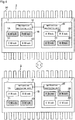
- the upper part shows a state where the first A block 1A and the first B block 1B enable function in the first chip 1, while the second C block 2C and the second D block 2D enable function in the second chip 2.
- the functional blocks to be enabled in the first chip 1 are changed to the first C block 1C and the first D block 1D
- the functional blocks to be enabled in the second chip 2 are changed to the second A block 2A and the second B block 2B.
- a heated state of the functional block may be changed depending on the operation mode of the semiconductor package 5, a heated state of the functional block may be changed. Therefore, it is possible to change the functional block to enable function depending on the operation mode so that the functional blocks to be enabled are distributed between the chips. In this way, depending on the heated state due to the operation mode, appropriate functional blocks can be distributed, and hence the longer life effect can be increased.
- the A block and the B block enable function and have temperatures of 70 degrees Celsius and 40 degrees Celsius, respectively, while the C block and the D block enable function and have temperatures of 50 degrees Celsius and 60 degrees Celsius, respectively.
- the first A block 1A and the first B block 1B enable function in the first chip 1
- the second C block 2C and the second D block 2D enable function in the second chip 2
- the functional blocks are distributed so that average temperatures of the chips are the same 55 degrees Celsius.
- the A block and the B block enable function and have temperatures of 70 degrees Celsius and 80 degrees Celsius, respectively, while the C block and the D block enable function and have temperatures of 50 degrees Celsius and 60 degrees Celsius. Therefore, in this another operation mode, it is possible that the first A block 1A and the first D block 1D enable function in the first chip 1, while the second B block 2B and the second C block 2C enable function in the second chip 2, and the functional blocks are distributed so that average temperatures in the chips are the same 65 degrees Celsius.
- the functional blocks are distributed so that two functional blocks are enabled in each of the first chip 1 and the second chip 2, but the numbers of the distributed functional blocks is not limited to the same number. For example, it is possible to distribute to one and three.
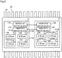
- FIG. 5 is a block diagram illustrating a schematic structure of a semiconductor package according to the second embodiment.
- a semiconductor package 15 according to the second embodiment illustrated in Fig. 5 includes a first chip 11 and a second chip 12.
- the first chip 11 includes a first A block 11A, a first B block 11B, a first C block 11C, a first D block 11D, a malfunction monitoring unit 11E, a temperature monitoring unit 11F, and temperature detecting units 111A to 111D.
- the second chip 12 includes a second A block 12A, a second B block 12B, a second C block 12C, a second D block 12D, a malfunction monitoring unit 12E, a temperature monitoring unit 12F, and temperature detecting units 121A to 121D.
- the functional blocks (A block to D block) and the malfunction monitoring units in the first chip 11 and the second chip 12 are the same as in the first embodiment described above.
- the temperature detecting units 111A to 111D are sensors arranged to detect temperatures of the first A block 11A to the first D block 11D, respectively.
- the temperature monitoring unit 11F monitors temperatures of the first A block 11A to the first D block 11 D based on detection signals output from the temperature detecting units 111A to 111D.
- the temperature detecting units 121A to 121D are sensors arranged to detect temperatures of the second A block 12A to the second D block 12D, respectively.
- the temperature monitoring unit 12F monitors temperatures of the second A block 12A to the second D block 12D based on detection signals output from the temperature detecting units 121A to 121D.
- One of the temperature monitoring unit 11F and the temperature monitoring unit 12F sends notification of the temperature monitor result to the other temperature monitoring unit via communication.
- the temperature monitoring unit that receives the notification is provided with temperature information of the functional blocks of both the first chip 1 and the second chip 2.
- This temperature monitoring unit determines functional blocks to enable function in the chip of itself and in the other chip based on the provided temperature information. Further, the temperature monitoring unit instructs to enable the determined functional blocks in the chip of itself and instructs to enable the functional blocks determined by the other temperature monitoring unit. In this way, the functional blocks are appropriately distributed between the first chip 11 and the second chip 12.
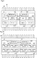
- the upper part shows a state where the first A block 11A and the first B block 11B enable function in the first chip 11, while the second C block 12C and the second D block 12D enable function in the second chip 12.
- the first A block 11A and the first B block 11B have temperatures of 70 degrees Celsius and 40 degrees Celsius, respectively
- the second C block 12C and the second D block 12D have temperatures of 60 degrees Celsius and 50 degrees Celsius, respectively.
- average temperatures of the chips are the same 55 degrees Celsius.
- the temperature monitoring unit 11F that monitors the temperatures of the first A block 11A and the first B block 11B sends notification of the temperature monitor result to the temperature monitoring unit 12F.
- the temperature monitoring unit 12F obtains temperature information of the second C block 12C and the second D block 12D monitored by itself, as well as temperature information of the first A block 11A and the first B block 11B.
- temperatures of the first A block 11A and the first B block 11B are 70 degrees Celsius and 80 degrees Celsius, respectively, while temperatures of the second C block 12C and the second D block 12D are 60 degrees Celsius and 50 degrees Celsius, respectively. Therefore, the temperature monitoring unit 12F determines to make the first A block 11A and the first C block 11C enable function in the first chip 11 and to make the second B block 12B and the second D block 12D enable function in the second chip 12, so that average temperatures becomes the same between the chips (the average temperatures becomes the same 65 degrees Celsius). On the basis of this determination, as shown in the lower part of Fig. 6 , the functional blocks to enable function are distributed between the first chip 11 and the second chip 12.
- the functional blocks are appropriately distributed between the chips, and hence the longer life effect of the semiconductor package 15 can be increased.
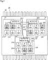
- FIG. 7 is a block diagram illustrating a schematic structure of a semiconductor package according to the third embodiment.
- a semiconductor package 25 illustrated in Fig. 7 includes a first chip 21, a second chip 22, and a third chip 23.
- the first chip 21 includes a firstAblock 21A, a first B block 21B, a first C block 21C, a first D block 21D, a first E block 21E, a first F block 21F, and a malfunction monitoring unit 21G.
- the second chip 22 includes a second A block 22A, a second B block 22B, a second C block 22C, a second D block 22D, a second E block 22E, a second F block 22F, and a malfunction monitoring unit 22G.
- the third chip 23 includes a third A block 23A, a third B block 23B, a third C block 23C, a third D block 23D, a third E block 23E, a third F block 23F, and a malfunction monitoring unit 23G.
- the malfunction monitoring units 21G, 22G, and 23G can communicate with each other.
- only one of the corresponding functional blocks having the same function among the first chip 21, the second chip 22, and the third chip 23 e.g. the first A block 21A, the second A block 22A, and the third A block 23A
- one or more functional blocks enable function in each of the first chip 21, the second chip 22, and the third chip 23.
- functional blocks are distributed among three chips, and hence longer life of the semiconductor package 25 is achieved.
- the first A block 21A and the first B block 21B enable function in the first chip 21, the second C block 22C and the second D block 22D enable function in the second chip 22, and the third E block 23E and the third F block 23F enable function in the third chip 23.
- temperatures of the first A block 21A and the first B block 21B are 50 degrees Celsius and 60 degrees Celsius, respectively.
- Temperatures of the second C block 22C and the second D block 22D are 60 degrees Celsius and 50 degrees Celsius, respectively.
- Temperatures of the third E block 23E and the third F block 23F are 45 degrees Celsius and 65 degrees Celsius, respectively. Average temperatures of the chips are the same 55 degrees Celsius.
- the malfunction monitoring units 21 G, 22G, and 23G respectively monitor whether or not the functional blocks the enable function in the first chip 21, the second chip 22, and the third chip 23 have a malfunction. Then, if one of the malfunction monitoring units 21 G, 22G, and 23G detects a malfunction of the functional block, the malfunction monitoring unit that has detected the malfunction sends notification to the other malfunction monitoring unit. Then, the malfunction monitoring units that receive the notification distribute functional blocks that enable function between the chips to which the malfunction monitoring units belong. In this case, the malfunction monitoring unit that has detected a malfunction disables all functional blocks of the chip to which the malfunction monitoring unit belongs.
- the functional blocks are distributed to other normal chips, so that a predetermined function is operated continuously as the semiconductor package 25, and hence longer life of the semiconductor package 25 can be achieved.
- the malfunction monitoring unit 21G detects that one of the first A block 21A and the first B block 21B that enable function has a malfunction in the first chip 21, the malfunction monitoring unit 21 G sends notification to the other malfunction monitoring units 22G and 23G.
- This state is illustrated in Fig. 8 .
- the malfunction monitoring unit 22G makes the second B block 22B, the second C block 22C, and the second E block 22E enable function in the second chip 22.
- the malfunction monitoring unit 23G makes the third A block 23A, the third D block 23D, and the third F block 23F enable function in the third chip 23.
- the malfunction monitoring unit 21G disables all functional blocks in the first chip 21.
- the functional blocks are distributed between the second chip 22 and the third chip 23, so that they have the same average temperature at 55 degrees Celsius, and hence longer life of the semiconductor package 25 can be achieved.
- the malfunction monitoring unit 22G further detects that one of the functional blocks in the second chip 22 has a malfunction, all functional blocks are disabled in the second chip 22, and the malfunction monitoring unit 22G sends notification to the malfunction monitoring unit 23G, so that all functional blocks are enabled in the third chip 23. In this way, a predetermined function can be operated continuously as the semiconductor package 25.
- Fig. 9 is a block diagram illustrating a schematic structure of a semiconductor package as a microcomputer according to an embodiment of the present invention.
- a semiconductor package 35 illustrated in Fig. 9 corresponds to a specific example of the semiconductor package of the first embodiment ( Fig. 1 ).
- the semiconductor package 35 includes a first chip 31 and a second chip 32.
- the first chip 31 includes a CPU 31A, a memory controller 31B, a memory 31C, an I/O unit 31D, and a malfunction monitoring unit 31E.
- the second chip 32 includes a CPU 32A, a memory controller 32B, a memory 32C, an I/O unit 32D, and a malfunction monitoring unit 32E.
- the CPU is a computing device including a program counter, an instruction decoder, an ALU, and the like.
- the memory controller is a device relaying between the CPU and the memory, and reads and writes data from and to the memory.
- the memory stores programs and data, and includes a RAM and a ROM.
- the I/O unit is an interface relaying between the CPU and an input/output device.
- the CPU 31A, the memory controller 31B, the memory 31C, and the I/O unit 31D correspond to functional blocks of the first A block 1A, the first B block 1B, the first C block 1C, and the first D block 1D, respectively in the first embodiment.
- the CPU 32A, the memory controller 32B, the memory 32C, and the I/O unit 32D correspond to functional blocks of the second A block 2A, the second B block 2B, the second C block 2C, and the second D block 2D, respectively in the first embodiment.
- the semiconductor package 35 functions as the microcomputer while generated heat is distributed, and hence longer life of the semiconductor package 35 can be achieved.
- the first embodiment but also the second embodiment (provided with the temperature detecting unit) or the third embodiment (three chips) can be applied to the semiconductor package as the microcomputer, and the actions and effects described in the embodiments can be obtained in the same manner.
- Fig. 10 is a block diagram illustrating a schematic structure of a semiconductor package as a power supply device according to an embodiment of the present invention.
- a semiconductor package 45 illustrated in Fig. 10 corresponds to a specific example of the semiconductor package of the first embodiment ( Fig. 1 ).
- the semiconductor package 45 illustrated in Fig. 10 includes a first chip 41 and a second chip 42.
- the first chip 41 includes a power supply block A 41A, a power supply block B 41B, a power supply block C 41C, a power supply block D 41D, and a malfunction monitoring unit 41E.
- the second chip 42 includes a power supply block A 42A, a power supply block B 42B, a power supply block C 42C, a power supply block D 42D, and a malfunction monitoring unit 42E.
- Each of the power supply blocks 41A to 41D and the power supply blocks 42A to 42D is constituted of a switching regulator or a series regulator. An output voltage generated from each power supply block is externally output from the corresponding lead frame 50.
- the power supply blocks 41A to 41D respectively correspond to the functional blocks of the first A block 1A, the first B block 1B, the first C block 1C, and the first D block 1D in the first embodiment.
- the power supply blocks 42A to 42D respectively correspond to the functional blocks of the second A block 2A, the second B block 2B, the second C block 2C, and the second D block 2D in the first embodiment.
- the output voltages output from the corresponding power supply blocks having the same function between the chips may be output from the common lead frame 50.
- the functional blocks that enable function are distributed between the first chip 41 and the second chip 42.
- the power supply block A 41A and the power supply block B 41B enable function in the first chip 41
- the power supply block C 42C and the power supply block D 42D enable function in the second chip 42.
- the semiconductor package 45 functions as the power supply device, and generated heat is distributed so that longer life of the semiconductor package 45 can be achieved.
- the first embodiment but also the second embodiment (provided with the temperature detecting unit) or the third embodiment (three chips) can be applied to the semiconductor package as the power supply device, and the actions and effects described in the embodiments can be obtained in the same manner.
- Fig. 11 is an external view of a structural example of a vehicle equipped with various electronic devices.
- a vehicle X of this structural example is equipped with a battery X10 and various electronic devices X11 to X18 that work with an input voltage supplied from the battery X10. Note that mounting positions of the battery X10 and the electronic devices X11 to X18 in Fig. 11 may be different from actual positions for convenience sake of illustration.
- the electronic device X11 is an engine control unit arranged to perform controls related to the engine (such as injection control, electronic throttle control, idling control, oxygen sensor heater control, and automatic cruise control).
- controls related to the engine such as injection control, electronic throttle control, idling control, oxygen sensor heater control, and automatic cruise control.
- the electronic device X12 is a lamp control unit arranged to perform on-off control of a high intensity discharged (HID) lamp, a daytime running lamp (DRL), and the like.
- HID high intensity discharged
- DRL daytime running lamp
- the electronic device X13 is a transmission control unit arranged to perform control related to a transmission.
- the electronic device X14 is a body control unit arranged to perform controls related to movement of the vehicle X (such as anti-lock brake system (ABS) control, electric power steering (EPS) control, and electronic suspension control).
- ABS anti-lock brake system
- EPS electric power steering
- E suspension control electronic suspension control
- the electronic device X15 is a security control unit arranged to perform control for driving a door lock, an anti-theft security alarm, and the like.
- the electronic device X16 is an electronic device such as a wiper, an electric door mirror, a power window, a damper (shock absorber), an electric sunroof, or an electric seat, which is mounted in the vehicle X at the shipping stage as standard equipment or a factory-installed option.
- the electronic device X17 is an electronic device such as an in-vehicle audio/visual (A/V) device, a car navigation system, or an electronic toll collection (ETC) system, which is mounted in the vehicle X as a user option.
- A/V in-vehicle audio/visual
- ETC electronic toll collection
- the electronic device X18 is an electronic device such as an in-vehicle blower, an oil pump, a water pump, or a battery cooling fan, which includes a high-voltage motor.
- the semiconductor package according to the embodiments described above can be incorporated in any of the electronic devices X11 to X18 as a microcomputer or a power supply device, for example.
- the technique of the embodiments described above is important for longer life and continuous operation even if a chip is broken down.
- FIG. 12 is a block diagram illustrating a schematic structure of a semiconductor package according to a fourth embodiment of the present invention.
- a semiconductor package 40 according to the fourth embodiment illustrated in Fig. 12 includes two chips (IC chips), i.e. a first chip 401 and a second chip 402, and is constituted of a multichip semiconductor package.
- the semiconductor package 40 functions as a microcomputer.
- the semiconductor package 40 has various lead frames 451.
- the first chip 401 and the second chip 402 are fixed to the lead frames 451. Electrodes of the first chip 401 and the second chip 402 are connected to the lead frames 451 with not-shown bonding wires (such as Au wires).
- the first chip 401, the second chip 402, and the lead frames 451 are sealed with resin.
- the lead frames 451 are connected to wirings of a not-shown printed circuit board so that the semiconductor package 40 is mounted on the printed circuit board. In this way, the first chip 401 and the second chip 402 can communicate electrical signals and powers with the printed circuit board.
- the first chip 401 include a magnetic field sensor 411 and a communication unit 412, which are integrated.
- the magnetic field sensor 411 (magnetic field detecting unit) is a sensor that detects a magnetic field M generated outside of the semiconductor package 40 and is constituted of a Hall element, for example.
- the communication unit 412 sends notification to a communication unit 425 of the second chip 402.
- the second chip 402 includes a CPU 421, a memory controller 422, a memory 423, an I/O unit 424, and the communication unit 425, which are integrated.
- the functional blocks of the CPU 421, the memory controller 422, the memory 423, and the I/O unit 424 realize functions as the microcomputer.
- the CPU 421 is a computing device including a program counter, an instruction decoder, an ALU, and the like.
- the memory controller 422 is a device relaying between the CPU 421 and the memory 423, and reads and writes data from and to the memory 423.
- the memory 423 stores programs and data, and includes a RAM, a ROM, and a nonvolatile memory.
- the I/O unit 424 is an interface relaying between the CPU 421 and an input/output device.
- the communication unit 425 When the communication unit 425 receives from the communication unit 412 the notification indicating that the magnetic field sensor 411 has detected the magnetic field M, it protects at least one of functional blocks of the CPU 421, the memory controller 422, the memory 423, and the I/O unit 424. In other words, the communication unit 425 functions as a protection unit, too.
- the communication unit 425 may stop operation of at least the CPU 421 among the CPU 421, the memory controller 422, and the I/O unit 424. In this way, it is possible to prevent the CPU 421 from having a malfunction by influence of the magnetic field M so that a malfunction occurs in the semiconductor package 40 as the microcomputer.
- the communication unit 425 may protect the memory 423 so as to prevent data stored in the memory 423 from being accidentally rewritten by influence of the magnetic field M. In this way, it is possible to prevent the semiconductor package 40 as the microcomputer from having a malfunction.
- the communication unit 425 may switch to a mode in which drive current of at least one of the CPU 421, the memory controller 422, and the I/O unit 424 is increased to operate the same. In this way, it is possible to protect the functional block that is apt to have a malfunction by influence of the magnetic field M when the drive current is small. Therefore, it is possible to continue stable operation of the semiconductor package 40 as the microcomputer.
- the communication unit 425 when the communication unit 425 receives the notification indicating that the magnetic field sensor 411 has detected the magnetic field M from the communication unit 412, it may make the memory controller 422 control the memory 423 to store information indicating that the magnetic field is generated. For example, by storing the information as current time information, it can be used for analyzing causes of malfunction.
- Fig. 13 is a block diagram illustrating a schematic structure of a semiconductor package according to a fifth embodiment of the present invention.
- a semiconductor package 55 of the fifth embodiment illustrated in Fig. 13 includes two chips (IC chips), i.e. a first chip 51 and a second chip 52, and is constituted of a multichip semiconductor package.
- the semiconductor package 55 functions as a power supply device.
- the semiconductor package 55 has various lead frames 551. Structures of the first chip 51, the second chip 52, and the lead frame 551, and a structure of mounting the semiconductor package 55 are the same as those of the first embodiment described above, and hence detailed description thereof is omitted.
- the first chip 51 includes a magnetic field sensor 511 and a communication unit 512, which are integrated.
- the magnetic field sensor 511 is a sensor that detects the magnetic field M generated outside of the semiconductor package 55 and is constituted of a Hall element, for example.
- the communication unit 512 sends notification to a communication unit 524 of the second chip 52.
- the second chip 52 includes a first power supply block 521, a second power supply block 522, a memory 523, and a communication unit 524, which are integrated.
- the functional blocks of the first power supply block 521 and the second power supply block 522 realize functions as the power supply device. Note that the number of the power supply blocks may be one or more and is not limited.
- the first power supply block 521 and the second power supply block 522 are circuits that generate output voltages based on a voltage supplied from outside via the lead frame 551, and are constituted of a switching regulator, a series regulator, or the like, for example.
- the memory 523 is constituted of a nonvolatile memory such as a flash memory.
- the communication unit 524 When the communication unit 524 receives the notification indicating that the magnetic field sensor 511 has detected the magnetic field M from the communication unit 512, it stops operation of at least one of the first power supply block 521 and the second power supply block 522 so as to protect them. In this way, it is possible to prevent a load of the first power supply block 521 or the second power supply block 522 from having a malfunction by influence of the magnetic field M.
- the communication unit 524 when the communication unit 524 receives the notification indicating that the magnetic field sensor 511 has detected the magnetic field M from the communication unit 512, it may make the memory 523 store information indicating that the magnetic field is generated.
- the information is stored as current time information, for example, and can be used for analyzing causes of malfunction.
- Fig. 14 is a schematic structural diagram illustrating an example of a case where the semiconductor package 40 according to the fourth embodiment (i.e. the microcomputer) is mounted in a vehicle.
- a vehicle 61 illustrated in Fig. 14 includes a power receiving unit 611, a charging unit 612, a travel motor controller 613, and a security controller 614.
- the vehicle 61 corresponds to a noncontact power supply system.
- the power receiving unit 611 receives power supplied from a power transmitting unit 60 installed on the ground side in a noncontact manner.
- An electromagnetic induction method or a magnetic field resonance method can be adopted for the noncontact power supply. Note that locations of the power receiving unit 611 and the power transmitting unit 60 are not limited to those illustrated in Fig. 14 .
- an AC current is supplied to a power transmission coil included in the power transmitting unit 60 to generate a magnetic field M, so that current is induced in a power receiving coil included in the power receiving unit 611.
- an LC circuit of a coil and a capacitor is disposed in each of the power transmitting unit 60 and the power receiving unit 611, and LC resonance of the magnetic field M is utilized to transmit power.
- the magnetic field M is generated when supplying power.
- the charging unit 612 includes a charge control unit, a battery, and the like, which are not-shown, and charges the battery with power received by the power receiving unit 611.
- the power stored in the battery is supplied to various electronic devices such as the travel motor controller 613 and the security controller 614, and is also supplied to a travel motor (not shown).
- the travel motor controller 613 is an electronic device arranged to perform control for driving the travel motor.
- a microcomputer 40A corresponding to the semiconductor package 40 is included in the travel motor controller 613.
- the security controller 614 is an electronic device arranged to perform control for driving a door lock, an anti-theft security alarm, and the like.
- a microcomputer 45B corresponding to the semiconductor package 45 is included in the security controller 614.
- the microcomputer 40A detects the generated magnetic field M by the structure of the fourth embodiment described above, and stops operation as the microcomputer, for example. In this way, it is possible to prevent the microcomputer 40A from having a malfunction by influence of the magnetic field M so that a malfunction occurs in control of the travel motor. For example, it is possible to prevent the vehicle 61 during a stop for power supply from accidentally starting to move.
- a microcomputer 40B detects the generated magnetic field M by the structure of the fourth embodiment described above, and stops operation as the microcomputer, for example. In this way, it is possible to prevent the microcomputer 40B from having a malfunction by influence of the magnetic field M so that a malfunction occurs in the security control. For example, it is possible to prevent the door lock of the vehicle 61 during a stop for power supply from being unlocked so that a theft may occur.
- the microcomputer 40A or 40B when the microcomputer 40A or 40B detects the magnetic field M, if the functional block is operated while increasing the drive current, the microcomputer 40A or 40B can continue the stable operation. Therefore, it is possible to prevent occurrence of a malfunction in the control of the travel motor or in the security control.
- microcomputer 40A or 40B it is preferred to position the microcomputer 40A or 40B in a vicinity of the power receiving unit 611, for example, so as to securely detect the magnetic field M when supplying power.
- FIG. 15 is a schematic structural diagram illustrating an example of a case where the semiconductor package 55 according to the fifth embodiment (i.e. the power supply device) is mounted in the vehicle.
- a vehicle 66 illustrated in Fig. 15 includes a power receiving unit 661, a charging unit 662, a travel motor controller 663, a security controller 664, and a power supply device 55A.
- the power supply device 55A corresponds to the semiconductor package 55 according to the fifth embodiment.
- a load of the first power supply block 521 of the semiconductor package 55 is the travel motor controller 663
- a load of the second power supply block 522 is the security controller 664.
- the power receiving unit 661 is supplied with power from a power transmitting unit 65 in a noncontact manner, and the charging unit 662 charges a not-shown battery with the supplied power, in the same manner as the example described above with reference to Fig. 14 .
- the power stored in the battery is supplied to the power supply device 55A and various electronic devices such as the travel motor controller 663 and the security controller 664.
- the power supply device 55A detects the generated magnetic field M by the structure of the fifth embodiment, and stops operation of the power supply block corresponding to the travel motor controller 663. In this way, it is possible to prevent the travel motor controller 663 as a load from having a malfunction by influence of the magnetic field M so that a malfunction occurs in the control of the travel motor.
- the power supply device 55A detects the generated magnetic field M by the structure of the fifth embodiment, and stops operation of the power supply block corresponding to the security controller 664. In this way, it is possible to prevent the security controller 664 as a load from having a malfunction by influence of the magnetic field M so that a malfunction occurs in the security control.
- the semiconductor package 40 or 55 according to the fourth or fifth embodiment described above can be appropriately incorporated in any of the electronic devices X11 to X18 mounted in the vehicle X illustrated in Fig. 11 , as the microcomputer or the power supply device.
- the technique of preventing a malfunction of an electronic device by influence of a magnetic field generated by noncontact power supply or the like is important.
- FIG. 16 is a schematic structural diagram illustrating an example of a case where the semiconductor package 40 according to the fourth embodiment (i.e. the microcomputer) is mounted in a smart phone (an example of the portable device).
- a smart phone 71 illustrated in Fig. 16 includes an antenna 711, a wireless communication unit 712, a camera unit 713, an operation unit 714, a GPS receiving unit 715, a gyro sensor 716, a storage unit 717, a power supply unit 718, a display unit 719, a control unit 720, a speaker 721, and a microphone 722.
- the wireless communication unit 712 performs wireless communication with a base station of a mobile communication network.
- the wireless communication is used to receive and transmit sound data, video data, electronic mail data, and the like, or to receive Web data, streaming data, and the like.
- the display unit 719 includes a touch panel 719A, a liquid crystal panel 719B, and a backlight 719C.
- the liquid crystal panel 719B is driven by the control unit 720, and liquid crystal corresponding to each pixel is driven according to an image to be displayed so that light transmittance is adjusted.
- the backlight 719C illuminates the liquid crystal panel 719B from backside, and an edge type using an LED and a light guide plate is adopted, for example.
- the touch panel 719A is placed on the liquid crystal panel 719B so that images displayed on a display screen of the liquid crystal panel 719B can be seen through it, and detects a touch by a user's finger or other object.
- the control unit 720 detects a touched position on the touch panel 719A based on a detection signal output from the touch panel 719A.
- the camera unit 713 takes an electronic image with an imaging device such as a CMOS image sensor, and the taken image is compressed by JPEG format, for example, and the compressed data can be stored in the storage unit 717.
- an imaging device such as a CMOS image sensor
- the operation unit 714 is an interface that receives an input from a user, and is constituted of buttons and the like.
- the GPS receiving unit 715 receives electromagnetic waves from GPS satellites and obtains positional information, which is output to the control unit 720.
- the gyro sensor 716 detects a direction (orientation) of the smart phone 71, and outputs orientation information to the control unit 720.
- the storage unit 717 stores address data including names and telephone numbers of communication opponents, transmitted or received electronic mail data, Web data downloaded by Web browsing, and downloaded contents data, and also temporarily stored streaming data and the like.
- the storage unit 717 is constituted of a flash memory, for example.
- the microphone 722 picks up voice of a user, the control unit 720 performs a predetermined process on the picked-up voice, and the wireless communication unit 712 transmits the voice to the base station.
- the voice received by the wireless communication unit 712 undergoes a predetermined process by the control unit 720 and is output from the speaker 721. In this way, users can talk over the phone.
- the speaker 721 can output not only the voice communication sound but also various sounds such as sound based on streaming data received by the wireless communication unit 712.
- the power supply unit 718 is a circuit that supplies power stored in a not-shown battery to individual portions of the smart phone 71.
- the control unit 720 includes a microcomputer 40C and integrally controls individual portions of the smart phone 71.
- the microcomputer 40C corresponds to the semiconductor package 40 according to the fourth embodiment.
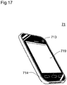
- FIG. 17 an external view of the smart phone 71 illustrated in Fig. 16 is shown in Fig. 17 , for example, in which the camera unit 713, the display unit 719, and the operation unit 714 are disposed on the front side of the smart phone 71.
- the smart phone 71 is carried by a user, and hence it is highly possible to position the smart phone 71 in a place where a magnetic field is generated.
- the smart phone 71 may be positioned in a vicinity of an IH cooker or a microwave oven that generate a magnetic field.
- the smart phone 71 may be exposed to a magnetic field when the user is in the vehicle that is being supplied with power in a noncontact manner as described above.
- the microcomputer 40C detects the generated magnetic field by the structure described above in the fourth embodiment and stops operation as the microcomputer, for example. In this way, it is possible to prevent the microcomputer 40C from having a malfunction by influence of the magnetic field so that a malfunction occurs in the smart phone 71.
- the microcomputer 40C when the microcomputer 40C detects the magnetic field and increases drive current for the functional block to operate, the microcomputer 40C can continue its stable operation. Therefore, it is possible to prevent a malfunction from occurring in the smart phone 71.
- Fig. 18 is a schematic structural diagram illustrating an example of a case where the semiconductor package 55 according to the fifth embodiment (i.e. the power supply device) is mounted in the smart phone.
- the structure of a smart phone 71' illustrated in Fig. 18 is basically the same as the structure described above with reference to Fig. 16 , and structural differences are that the control unit 720 includes a microcomputer 720A, and that the power supply unit 718 includes a power supply device 55B.
- the power supply device 55B corresponds to the semiconductor package 55 according to the fifth embodiment.
- An output voltage generated by the power supply device 55B is supplied to the microcomputer 720A as a load.
- the power supply device 55B detects the magnetic field by the structure described above in the fifth embodiment and stops the power supply block that supplies voltage to the microcomputer 720A (e.g. the first power supply block 521). In this way, it is possible to prevent the microcomputer 720A from having a malfunction by influence of the magnetic field so that a malfunction occurs in the smart phone 71'.
- the semiconductor package of the embodiment described above can be applied not only to the smart phone but also to various portable devices such as a tablet computer.
Landscapes
- Engineering & Computer Science (AREA)
- Theoretical Computer Science (AREA)
- Physics & Mathematics (AREA)
- General Engineering & Computer Science (AREA)
- General Physics & Mathematics (AREA)
- Semiconductor Integrated Circuits (AREA)
- Automation & Control Theory (AREA)
- Manufacturing & Machinery (AREA)
- Microelectronics & Electronic Packaging (AREA)
- Dicing (AREA)
Abstract
Description
- This nonprovisional application claims priority under 35 U.S.C. § 119(a) on Patent Applications No.
2016-166487 2016-166488 2017-122392 - The present invention relates to a semiconductor package.
- Conventionally, semiconductor packages are developed for use as a microcomputer, a power supply device, and the like, and the semiconductor packages are mounted in various devices.
- Note that examples of conventional techniques related to the above description are disclosed in
JP-A-2007-257028 JP-A-2000-88680 - The semiconductor package described above may be constituted for in-vehicle use in particular these days. For example, a semiconductor package as a microcomputer may be incorporated in an electronic control unit (ECU) mounted in a vehicle.
- In the vehicle related field, ISO26262 or the like as an international standard for electric/electronic functional safety of a vehicle is laid down, and in this situation, in order to attach more importance to safety, it is particularly required to achieve longer life of semiconductor packages mounted in vehicles.
- In addition, along with widespread use of electric vehicle (EV) and the like, a power supply system that supplies power to a vehicle in a noncontact manner is developed recently. When supplying power with this power supply system, a strong magnetic field is generated, and hence a microcomputer mounted in the stopped vehicle may cause a malfunction. This malfunction may cause the vehicle to erroneously start to drive or to erroneously unlock a door.
- In the vehicle related field, ISO26262 or the like as an international standard for electric/electronic functional safety of a vehicle is laid down, and hence more safety is required as the situation.
- In view of the situation described above, it is a first object of the present invention to provide a semiconductor package capable of achieving a longer life. In addition, it is a second object of the present invention to provide a semiconductor package capable of preventing an electronic device from having a malfunction by influence of a magnetic field.
- A semiconductor device according to one aspect of the present invention includes a plurality of chips. The plurality of chips include a plurality of corresponding functional blocks having the same function among the chips. Only one of the corresponding functional blocks having the same function among the chips enables function, and one or more functional blocks enable function in each of the chips so that the functional blocks are distributed among the chips.
- A semiconductor device according to another aspect of the present invention includes one or more functional blocks, a magnetic field detecting unit arranged to detect a magnetic field, and a protection unit arranged to protect at least one of the functional blocks when the magnetic field detecting unit detects a magnetic field.
-
-
Fig. 1 is a block diagram illustrating a schematic structure of a semiconductor package according to a first embodiment of the present invention. -
Fig. 2 is a diagram illustrating an example of distribution of functional blocks in the semiconductor package according to the first embodiment of the present invention. -
Fig. 3 is a diagram illustrating an example of a case where a malfunction of a chip occurs in the semiconductor package according to the first embodiment of the present invention. -
Fig. 4 is a diagram illustrating an example where the functional blocks are changed and distributed in the semiconductor package according to the first embodiment of the present invention. -
Fig. 5 is a block diagram illustrating a schematic structure of a semiconductor package according to a second embodiment of the present invention. -
Fig. 6 is a diagram illustrating an example where the functional blocks are changed and distributed in the semiconductor package according to the second embodiment of the present invention. -
Fig. 7 is a block diagram illustrating a schematic structure of a semiconductor package according to a third embodiment of the present invention. -
Fig. 8 is a diagram illustrating an example of a case where a malfunction of a chip occurs in the semiconductor package according to the third embodiment of the present invention. -
Fig. 9 is a schematic structural diagram illustrating an example of a semiconductor package functioning as a microcomputer. -
Fig. 10 is a schematic structural diagram illustrating an example of a semiconductor package functioning as a power supply device. -
Fig. 11 is an external view illustrating a structural example of a vehicle equipped with various electronic devices. -
Fig. 12 is a block diagram illustrating a schematic structure of a semiconductor package according to a fourth embodiment of the present invention. -
Fig. 13 is a block diagram illustrating a schematic structure of a semiconductor package according to a fifth embodiment of the present invention. -
Fig. 14 is a schematic structural diagram illustrating an example where the semiconductor package according to the fourth embodiment of the present invention is mounted in a vehicle. -
Fig. 15 is a schematic structural diagram illustrating an example where the semiconductor package according to the fifth embodiment of the present invention is mounted in a vehicle. -
Fig. 16 is a schematic structural diagram illustrating an example of a smart phone equipped with the semiconductor package according to the fourth embodiment of the present invention. -
Fig. 17 is a diagram illustrating an example of an external view of the smart phone. -
Fig. 18 is a schematic structural diagram illustrating an example of a smart phone equipped with the semiconductor package according to the fifth embodiment of the present invention. - Hereinafter, embodiments of the present invention are described with reference to the drawings.
-
Fig. 1 is a block diagram illustrating a schematic structure of a semiconductor package according to a first embodiment of the present invention. Asemiconductor package 5 according to the first embodiment illustrated inFig. 1 includes two chips (IC chips), i.e. afirst chip 1 and asecond chip 2, and is constituted as a multichip semiconductor package. - In addition, the
semiconductor package 5 has various lead frames (pins) 50. Thefirst chip 1 and thesecond chip 2 are fixed to thelead frames 50. Electrodes of thefirst chip 1 and thesecond chip 2 are connected to thelead frames 50 with not-shown bonding wires (such as Au wires). Thefirst chip 1, thesecond chip 2, and thelead frames 50 are sealed with resin. Thelead frames 50 are connected to wirings of a not-shown printed circuit board so that thesemiconductor package 5 is mounted on the printed circuit board. In this way, thefirst chip 1 and thesecond chip 2 can communicate electrical signals and powers with the printed circuit board. - The
first chip 1 includes afirst A block 1A, afirst B block 1B, afirst C block 1C, afirst D block 1D, and amalfunction monitoring unit 1E. Thesecond chip 2 includes asecond A block 2A, asecond B block 2B, asecond C block 2C, asecond D block 2D, and amalfunction monitoring unit 2E. Themalfunction monitoring unit 1E and themalfunction monitoring unit 2E can communicate with each other. - The
first A block 1A and thesecond A block 2A are functional blocks having the same function. In the same manner, thefirst B block 1B and thesecond B block 2B are functional blocks having the same function, thefirst C block 1C and thesecond C block 2C are functional blocks having the same function, and thefirst D block 1D and thesecond D block 2D are functional blocks having the same function. - In this embodiment, only one of corresponding function blocks having the same function (e.g. the
first A block 1A and thesecond A block 2A) between thefirst chip 1 and thesecond chip 2 enables function, and one or more functional blocks enable function in each of thefirst chip 1 and thesecond chip 2. - In this way, a predetermined function is realized as the
entire semiconductor package 5, and heat generated in the functional blocks by enabling function can be distributed to different chips, and hence life of thesemiconductor package 5 can be elongated. In this case, it is preferred to decrease a difference between average temperature due to heat generated by the functional block enabling function in thefirst chip 1 and average temperature due to heat generated by the functional block enabling function in thesecond chip 2, as much as possible. - For example, in the example illustrated in
Fig. 2 , thefirst chip 1 and thesecond chip 2 respectively include thefirst A block 1A and thesecond A block 2A, which are corresponding functional blocks having the same function, and only thefirst A block 1A enables function (operates) while thesecond A block 2A disables function (stops operation). In the same manner, only thefirst B block 1B enables function between thefirst B block 1B and thesecond B block 2B, only thesecond C block 2C enables function between thefirst C block 1C and thesecond C block 2C, and only thesecond D block 2D enables function between thefirst D block 1D and thesecond D block 2D. In addition, two functional blocks enable function in thefirst chip 1, and two functional blocks enable function in thesecond chip 2. - In this case, it is supposed that temperatures of the
first A block 1A and thefirst B block 1B due to heat generation are 70 degrees Celsius and 40 degrees Celsius, respectively, and that temperatures of thesecond C block 2C and thesecond D block 2D due to heat generation are 50 degrees Celsius and 60 degrees Celsius, respectively, for example. Then, average temperatures in thefirst chip 1 and thesecond chip 2 are both 55 degrees Celsius, and there is no difference between the average temperatures, which is advantageous for longer life of thesemiconductor package 5. - In addition, in this embodiment, in a normal operation, the
malfunction monitoring unit 1E monitors whether or not the functional block that enables function in thefirst chip 1 has a malfunction, and themalfunction monitoring unit 2E monitors whether or not the functional block that enables function in thesecond chip 2 has a malfunction. Then, if one of themalfunction monitoring unit 1E and themalfunction monitoring unit 2E detects a malfunction of the functional block, the malfunction monitoring unit that has detected the malfunction sends notification to the other malfunction monitoring unit. In this way, the malfunction monitoring unit that receives the notification enables all functional blocks of the chip on this malfunction monitoring unit side (i.e. the normal chip). On the other hand, the malfunction monitoring unit that has detected a malfunction disables all functions of the chip on this malfunction monitoring unit side. - In this way, between the
first chip 1 and thesecond chip 2, the chip in which a malfunction is detected disables function, and the other normal chip can continue to operate a predetermined function as the entire semiconductor package 3. - For example, in the example illustrated in
Fig. 3 , there is described a case where themalfunction monitoring unit 1E detects a malfunction in one of thefirst A block 1A and thefirst B block 1B that enable function in thefirst chip 1 as described above with reference toFig. 2 , and themalfunction monitoring unit 1E sends notification to themalfunction monitoring unit 2E. In this case, themalfunction monitoring unit 2E that received the notification enables all functional blocks of the second chip 2 (thesecond A block 2A to thesecond D block 2D), while themalfunction monitoring unit 1E disables all functional blocks of thefirst chip 1. - As described above, in this embodiment, the functional blocks that enable function are distributed between the
first chip 1 and thesecond chip 2. However, instead of always enabling only the fixed functional block, it is possible to change the functional block to be enabled while the functional blocks to be enabled may be distributed between the chips. In this way, the structure becomes more advantageous for longer life. - For example, in the example illustrated in
Fig. 4 , the upper part shows a state where thefirst A block 1A and thefirst B block 1B enable function in thefirst chip 1, while thesecond C block 2C and thesecond D block 2D enable function in thesecond chip 2. Then, as shown in the lower part, from the state described above, the functional blocks to be enabled in thefirst chip 1 are changed to thefirst C block 1C and thefirst D block 1D, and the functional blocks to be enabled in thesecond chip 2 are changed to thesecond A block 2A and thesecond B block 2B. These states illustrated in the upper part and the lower part ofFig. 4 are sequentially repeated. Note that switching of the states may be performed, for example, every time when the number of start-up times of thesemiconductor package 5 reaches a predetermined number. - In addition, depending on the operation mode of the
semiconductor package 5, a heated state of the functional block may be changed. Therefore, it is possible to change the functional block to enable function depending on the operation mode so that the functional blocks to be enabled are distributed between the chips. In this way, depending on the heated state due to the operation mode, appropriate functional blocks can be distributed, and hence the longer life effect can be increased. - For example, it is supposed that in an certain operation mode, the A block and the B block enable function and have temperatures of 70 degrees Celsius and 40 degrees Celsius, respectively, while the C block and the D block enable function and have temperatures of 50 degrees Celsius and 60 degrees Celsius, respectively. Then, it is supposed that in this operation mode, as illustrated in
Fig. 2 , thefirst A block 1A and thefirst B block 1B enable function in thefirst chip 1, while thesecond C block 2C and thesecond D block 2D enable function in thesecond chip 2, and the functional blocks are distributed so that average temperatures of the chips are the same 55 degrees Celsius. - In this case, it is supposed that in another operation mode, the A block and the B block enable function and have temperatures of 70 degrees Celsius and 80 degrees Celsius, respectively, while the C block and the D block enable function and have temperatures of 50 degrees Celsius and 60 degrees Celsius. Therefore, in this another operation mode, it is possible that the
first A block 1A and thefirst D block 1D enable function in thefirst chip 1, while thesecond B block 2B and the second C block 2C enable function in thesecond chip 2, and the functional blocks are distributed so that average temperatures in the chips are the same 65 degrees Celsius. - Note that in the example described above, the functional blocks are distributed so that two functional blocks are enabled in each of the
first chip 1 and thesecond chip 2, but the numbers of the distributed functional blocks is not limited to the same number. For example, it is possible to distribute to one and three. - Next, a second embodiment of the present invention is described.
Fig. 5 is a block diagram illustrating a schematic structure of a semiconductor package according to the second embodiment. Asemiconductor package 15 according to the second embodiment illustrated inFig. 5 includes a first chip 11 and asecond chip 12. - The first chip 11 includes a
first A block 11A, afirst B block 11B, a first C block 11C, afirst D block 11D, amalfunction monitoring unit 11E, atemperature monitoring unit 11F, andtemperature detecting units 111A to 111D. - The
second chip 12 includes asecond A block 12A, asecond B block 12B, a second C block 12C, asecond D block 12D, amalfunction monitoring unit 12E, atemperature monitoring unit 12F, andtemperature detecting units 121A to 121D. - The functional blocks (A block to D block) and the malfunction monitoring units in the first chip 11 and the
second chip 12 are the same as in the first embodiment described above. Thetemperature detecting units 111A to 111D are sensors arranged to detect temperatures of thefirst A block 11A to thefirst D block 11D, respectively. Thetemperature monitoring unit 11F monitors temperatures of thefirst A block 11A to thefirst D block 11 D based on detection signals output from thetemperature detecting units 111A to 111D. - The
temperature detecting units 121A to 121D are sensors arranged to detect temperatures of thesecond A block 12A to thesecond D block 12D, respectively. Thetemperature monitoring unit 12F monitors temperatures of thesecond A block 12A to thesecond D block 12D based on detection signals output from thetemperature detecting units 121A to 121D. - One of the
temperature monitoring unit 11F and thetemperature monitoring unit 12F sends notification of the temperature monitor result to the other temperature monitoring unit via communication. In this way, the temperature monitoring unit that receives the notification is provided with temperature information of the functional blocks of both thefirst chip 1 and thesecond chip 2. This temperature monitoring unit determines functional blocks to enable function in the chip of itself and in the other chip based on the provided temperature information. Further, the temperature monitoring unit instructs to enable the determined functional blocks in the chip of itself and instructs to enable the functional blocks determined by the other temperature monitoring unit. In this way, the functional blocks are appropriately distributed between the first chip 11 and thesecond chip 12. - For example, in the example illustrated in
Fig. 6 , the upper part shows a state where thefirst A block 11A and the first B block 11B enable function in the first chip 11, while the second C block 12C and thesecond D block 12D enable function in thesecond chip 12. In this case, thefirst A block 11A and thefirst B block 11B have temperatures of 70 degrees Celsius and 40 degrees Celsius, respectively, while the second C block 12C and thesecond D block 12D have temperatures of 60 degrees Celsius and 50 degrees Celsius, respectively. Thus, average temperatures of the chips are the same 55 degrees Celsius. - After that, it is supposed that the heated state is changed, and the temperature of the
first B block 11B that enables function is increased up to 80 degrees Celsius. Then, thetemperature monitoring unit 11F that monitors the temperatures of thefirst A block 11A and thefirst B block 11B sends notification of the temperature monitor result to thetemperature monitoring unit 12F. Thetemperature monitoring unit 12F obtains temperature information of the second C block 12C and thesecond D block 12D monitored by itself, as well as temperature information of thefirst A block 11A and thefirst B block 11B. - In this case, temperatures of the
first A block 11A and thefirst B block 11B are 70 degrees Celsius and 80 degrees Celsius, respectively, while temperatures of the second C block 12C and thesecond D block 12D are 60 degrees Celsius and 50 degrees Celsius, respectively. Therefore, thetemperature monitoring unit 12F determines to make thefirst A block 11A and the first C block 11C enable function in the first chip 11 and to make the second B block 12B and thesecond D block 12D enable function in thesecond chip 12, so that average temperatures becomes the same between the chips (the average temperatures becomes the same 65 degrees Celsius). On the basis of this determination, as shown in the lower part ofFig. 6 , the functional blocks to enable function are distributed between the first chip 11 and thesecond chip 12. - With this embodiment, for example, not only according to different operation modes but also in a case where the heated state is changed in the same operation mode, the functional blocks are appropriately distributed between the chips, and hence the longer life effect of the
semiconductor package 15 can be increased. - Next, a third embodiment of the present invention is described.
Fig. 7 is a block diagram illustrating a schematic structure of a semiconductor package according to the third embodiment. Asemiconductor package 25 illustrated inFig. 7 includes afirst chip 21, asecond chip 22, and a third chip 23. - The
first chip 21 includes a firstAblock 21A, a first B block 21B, afirst C block 21C, afirst D block 21D, afirst E block 21E, afirst F block 21F, and amalfunction monitoring unit 21G. - The
second chip 22 includes asecond A block 22A, asecond B block 22B, asecond C block 22C, a second D block 22D, asecond E block 22E, asecond F block 22F, and amalfunction monitoring unit 22G. - The third chip 23 includes a
third A block 23A, athird B block 23B, athird C block 23C, athird D block 23D, athird E block 23E, athird F block 23F, and a malfunction monitoring unit 23G. - The
malfunction monitoring units - In this embodiment, in the normal operation, only one of the corresponding functional blocks having the same function among the
first chip 21, thesecond chip 22, and the third chip 23 (e.g. the first A block 21A, thesecond A block 22A, and thethird A block 23A) enables function, and one or more functional blocks enable function in each of thefirst chip 21, thesecond chip 22, and the third chip 23. In this way, functional blocks are distributed among three chips, and hence longer life of thesemiconductor package 25 is achieved. - For example, in the example of
Fig. 7 , the first A block 21A and the first B block 21B enable function in thefirst chip 21, thesecond C block 22C and the second D block 22D enable function in thesecond chip 22, and thethird E block 23E and thethird F block 23F enable function in the third chip 23. In this case, for example, temperatures of the first A block 21A and the first B block 21B are 50 degrees Celsius and 60 degrees Celsius, respectively. Temperatures of thesecond C block 22C and the second D block 22D are 60 degrees Celsius and 50 degrees Celsius, respectively. Temperatures of thethird E block 23E and thethird F block 23F are 45 degrees Celsius and 65 degrees Celsius, respectively. Average temperatures of the chips are the same 55 degrees Celsius. - In this embodiment, in the normal operation, the
malfunction monitoring units first chip 21, thesecond chip 22, and the third chip 23 have a malfunction. Then, if one of themalfunction monitoring units - In this way, even if one of the chips has a malfunction, the functional blocks are distributed to other normal chips, so that a predetermined function is operated continuously as the
semiconductor package 25, and hence longer life of thesemiconductor package 25 can be achieved. - For example, in the example of
Fig. 7 , if themalfunction monitoring unit 21G detects that one of the first A block 21A and the first B block 21B that enable function has a malfunction in thefirst chip 21, themalfunction monitoring unit 21 G sends notification to the othermalfunction monitoring units 22G and 23G. This state is illustrated inFig. 8 . In this way, themalfunction monitoring unit 22G makes thesecond B block 22B, thesecond C block 22C, and the second E block 22E enable function in thesecond chip 22. In this case, the malfunction monitoring unit 23G makes thethird A block 23A, thethird D block 23D, and thethird F block 23F enable function in the third chip 23. In addition, themalfunction monitoring unit 21G disables all functional blocks in thefirst chip 21. - In this way, the functional blocks are distributed between the
second chip 22 and the third chip 23, so that they have the same average temperature at 55 degrees Celsius, and hence longer life of thesemiconductor package 25 can be achieved. - Note that in the state of
Fig. 8 , if themalfunction monitoring unit 22G further detects that one of the functional blocks in thesecond chip 22 has a malfunction, all functional blocks are disabled in thesecond chip 22, and themalfunction monitoring unit 22G sends notification to the malfunction monitoring unit 23G, so that all functional blocks are enabled in the third chip 23. In this way, a predetermined function can be operated continuously as thesemiconductor package 25. - Hereinafter, specific examples of the embodiment described above are described.
-
Fig. 9 is a block diagram illustrating a schematic structure of a semiconductor package as a microcomputer according to an embodiment of the present invention. Asemiconductor package 35 illustrated inFig. 9 corresponds to a specific example of the semiconductor package of the first embodiment (Fig. 1 ). - The
semiconductor package 35 includes a first chip 31 and asecond chip 32. The first chip 31 includes aCPU 31A, amemory controller 31B, amemory 31C, an I/O unit 31D, and amalfunction monitoring unit 31E. Thesecond chip 32 includes aCPU 32A, amemory controller 32B, amemory 32C, an I/O unit 32D, and amalfunction monitoring unit 32E. - The CPU is a computing device including a program counter, an instruction decoder, an ALU, and the like. The memory controller is a device relaying between the CPU and the memory, and reads and writes data from and to the memory. The memory stores programs and data, and includes a RAM and a ROM. The I/O unit is an interface relaying between the CPU and an input/output device.
- The
CPU 31A, thememory controller 31B, thememory 31C, and the I/O unit 31D correspond to functional blocks of thefirst A block 1A, thefirst B block 1B, thefirst C block 1C, and thefirst D block 1D, respectively in the first embodiment. - The
CPU 32A, thememory controller 32B, thememory 32C, and the I/O unit 32D correspond to functional blocks of thesecond A block 2A, thesecond B block 2B, thesecond C block 2C, and thesecond D block 2D, respectively in the first embodiment. - Therefore, in the same manner as the first embodiment, functional blocks that enable function are distributed between the first chip 31 and the
second chip 32. For example, theCPU 31A and thememory controller 31B enable function in the first chip 31, while thememory 32C and the I/O unit 32D enable function in thesecond chip 32. In this way, thesemiconductor package 35 functions as the microcomputer while generated heat is distributed, and hence longer life of thesemiconductor package 35 can be achieved. - Note that when functional blocks such as the memory controller and the memory, or the CPU and the I/O unit, which need to communicate with each other, are distributed between the first chip 31 and the
second chip 32, communication between the functional block is performed via communication between the chips. - Note that not only the first embodiment but also the second embodiment (provided with the temperature detecting unit) or the third embodiment (three chips) can be applied to the semiconductor package as the microcomputer, and the actions and effects described in the embodiments can be obtained in the same manner.
-
Fig. 10 is a block diagram illustrating a schematic structure of a semiconductor package as a power supply device according to an embodiment of the present invention. Asemiconductor package 45 illustrated inFig. 10 corresponds to a specific example of the semiconductor package of the first embodiment (Fig. 1 ). - The
semiconductor package 45 illustrated inFig. 10 includes afirst chip 41 and asecond chip 42. Thefirst chip 41 includes a powersupply block A 41A, a powersupply block B 41B, a powersupply block C 41C, a powersupply block D 41D, and amalfunction monitoring unit 41E. Thesecond chip 42 includes a powersupply block A 42A, a powersupply block B 42B, a powersupply block C 42C, a powersupply block D 42D, and amalfunction monitoring unit 42E. - Each of the power supply blocks 41A to 41D and the power supply blocks 42A to 42D is constituted of a switching regulator or a series regulator. An output voltage generated from each power supply block is externally output from the
corresponding lead frame 50. - The power supply blocks 41A to 41D respectively correspond to the functional blocks of the
first A block 1A, thefirst B block 1B, thefirst C block 1C, and thefirst D block 1D in the first embodiment. - The power supply blocks 42A to 42D respectively correspond to the functional blocks of the
second A block 2A, thesecond B block 2B, thesecond C block 2C, and thesecond D block 2D in the first embodiment. - The output voltages output from the corresponding power supply blocks having the same function between the chips (e.g. the power
supply block A 41A and the powersupply block A 42A) may be output from thecommon lead frame 50. - In the same manner as the first embodiment, the functional blocks that enable function are distributed between the
first chip 41 and thesecond chip 42. For example, the powersupply block A 41A and the powersupply block B 41B enable function in thefirst chip 41, while the powersupply block C 42C and the powersupply block D 42D enable function in thesecond chip 42. In this way, thesemiconductor package 45 functions as the power supply device, and generated heat is distributed so that longer life of thesemiconductor package 45 can be achieved. - Note that not only the first embodiment but also the second embodiment (provided with the temperature detecting unit) or the third embodiment (three chips) can be applied to the semiconductor package as the power supply device, and the actions and effects described in the embodiments can be obtained in the same manner.
-
Fig. 11 is an external view of a structural example of a vehicle equipped with various electronic devices. A vehicle X of this structural example is equipped with a battery X10 and various electronic devices X11 to X18 that work with an input voltage supplied from the battery X10. Note that mounting positions of the battery X10 and the electronic devices X11 to X18 inFig. 11 may be different from actual positions for convenience sake of illustration. - The electronic device X11 is an engine control unit arranged to perform controls related to the engine (such as injection control, electronic throttle control, idling control, oxygen sensor heater control, and automatic cruise control).
- The electronic device X12 is a lamp control unit arranged to perform on-off control of a high intensity discharged (HID) lamp, a daytime running lamp (DRL), and the like.
- The electronic device X13 is a transmission control unit arranged to perform control related to a transmission.
- The electronic device X14 is a body control unit arranged to perform controls related to movement of the vehicle X (such as anti-lock brake system (ABS) control, electric power steering (EPS) control, and electronic suspension control).
- The electronic device X15 is a security control unit arranged to perform control for driving a door lock, an anti-theft security alarm, and the like.
- The electronic device X16 is an electronic device such as a wiper, an electric door mirror, a power window, a damper (shock absorber), an electric sunroof, or an electric seat, which is mounted in the vehicle X at the shipping stage as standard equipment or a factory-installed option.
- The electronic device X17 is an electronic device such as an in-vehicle audio/visual (A/V) device, a car navigation system, or an electronic toll collection (ETC) system, which is mounted in the vehicle X as a user option.
- The electronic device X18 is an electronic device such as an in-vehicle blower, an oil pump, a water pump, or a battery cooling fan, which includes a high-voltage motor.
- Note that the semiconductor package according to the embodiments described above can be incorporated in any of the electronic devices X11 to X18 as a microcomputer or a power supply device, for example. In particular, in the recent situation where ISO26262 or the like for in-vehicle devices is laid down, the technique of the embodiments described above is important for longer life and continuous operation even if a chip is broken down.
-
Fig. 12 is a block diagram illustrating a schematic structure of a semiconductor package according to a fourth embodiment of the present invention. Asemiconductor package 40 according to the fourth embodiment illustrated inFig. 12 includes two chips (IC chips), i.e. afirst chip 401 and asecond chip 402, and is constituted of a multichip semiconductor package. Thesemiconductor package 40 functions as a microcomputer. - The
semiconductor package 40 has various lead frames 451. Thefirst chip 401 and thesecond chip 402 are fixed to the lead frames 451. Electrodes of thefirst chip 401 and thesecond chip 402 are connected to the lead frames 451 with not-shown bonding wires (such as Au wires). Thefirst chip 401, thesecond chip 402, and the lead frames 451 are sealed with resin. The lead frames 451 are connected to wirings of a not-shown printed circuit board so that thesemiconductor package 40 is mounted on the printed circuit board. In this way, thefirst chip 401 and thesecond chip 402 can communicate electrical signals and powers with the printed circuit board. - The
first chip 401 include amagnetic field sensor 411 and acommunication unit 412, which are integrated. The magnetic field sensor 411 (magnetic field detecting unit) is a sensor that detects a magnetic field M generated outside of thesemiconductor package 40 and is constituted of a Hall element, for example. When themagnetic field sensor 411 detects the magnetic field M, thecommunication unit 412 sends notification to acommunication unit 425 of thesecond chip 402. - The
second chip 402 includes aCPU 421, amemory controller 422, amemory 423, an I/O unit 424, and thecommunication unit 425, which are integrated. The functional blocks of theCPU 421, thememory controller 422, thememory 423, and the I/O unit 424 realize functions as the microcomputer. - The
CPU 421 is a computing device including a program counter, an instruction decoder, an ALU, and the like. Thememory controller 422 is a device relaying between theCPU 421 and thememory 423, and reads and writes data from and to thememory 423. Thememory 423 stores programs and data, and includes a RAM, a ROM, and a nonvolatile memory. The I/O unit 424 is an interface relaying between theCPU 421 and an input/output device. - When the
communication unit 425 receives from thecommunication unit 412 the notification indicating that themagnetic field sensor 411 has detected the magnetic field M, it protects at least one of functional blocks of theCPU 421, thememory controller 422, thememory 423, and the I/O unit 424. In other words, thecommunication unit 425 functions as a protection unit, too. - For example, the
communication unit 425 may stop operation of at least theCPU 421 among theCPU 421, thememory controller 422, and the I/O unit 424. In this way, it is possible to prevent theCPU 421 from having a malfunction by influence of the magnetic field M so that a malfunction occurs in thesemiconductor package 40 as the microcomputer. - In addition, for example, the
communication unit 425 may protect thememory 423 so as to prevent data stored in thememory 423 from being accidentally rewritten by influence of the magnetic field M. In this way, it is possible to prevent thesemiconductor package 40 as the microcomputer from having a malfunction. - In addition, for example, the
communication unit 425 may switch to a mode in which drive current of at least one of theCPU 421, thememory controller 422, and the I/O unit 424 is increased to operate the same. In this way, it is possible to protect the functional block that is apt to have a malfunction by influence of the magnetic field M when the drive current is small. Therefore, it is possible to continue stable operation of thesemiconductor package 40 as the microcomputer. - In addition, when the
communication unit 425 receives the notification indicating that themagnetic field sensor 411 has detected the magnetic field M from thecommunication unit 412, it may make thememory controller 422 control thememory 423 to store information indicating that the magnetic field is generated. For example, by storing the information as current time information, it can be used for analyzing causes of malfunction. - Note that it is not always necessary to divide the structural elements of the
semiconductor package 40 into two, i.e. thefirst chip 401 and thesecond chip 402, but all structural elements may be constituted in one chip. -
Fig. 13 is a block diagram illustrating a schematic structure of a semiconductor package according to a fifth embodiment of the present invention. Asemiconductor package 55 of the fifth embodiment illustrated inFig. 13 includes two chips (IC chips), i.e. a first chip 51 and asecond chip 52, and is constituted of a multichip semiconductor package. Thesemiconductor package 55 functions as a power supply device. - The
semiconductor package 55 has various lead frames 551. Structures of the first chip 51, thesecond chip 52, and thelead frame 551, and a structure of mounting thesemiconductor package 55 are the same as those of the first embodiment described above, and hence detailed description thereof is omitted. - The first chip 51 includes a
magnetic field sensor 511 and acommunication unit 512, which are integrated. Themagnetic field sensor 511 is a sensor that detects the magnetic field M generated outside of thesemiconductor package 55 and is constituted of a Hall element, for example. When themagnetic field sensor 511 detects the magnetic field M, thecommunication unit 512 sends notification to acommunication unit 524 of thesecond chip 52. - The
second chip 52 includes a firstpower supply block 521, a secondpower supply block 522, amemory 523, and acommunication unit 524, which are integrated. The functional blocks of the firstpower supply block 521 and the secondpower supply block 522 realize functions as the power supply device. Note that the number of the power supply blocks may be one or more and is not limited. - The first
power supply block 521 and the secondpower supply block 522 are circuits that generate output voltages based on a voltage supplied from outside via thelead frame 551, and are constituted of a switching regulator, a series regulator, or the like, for example. Thememory 523 is constituted of a nonvolatile memory such as a flash memory. - When the
communication unit 524 receives the notification indicating that themagnetic field sensor 511 has detected the magnetic field M from thecommunication unit 512, it stops operation of at least one of the firstpower supply block 521 and the secondpower supply block 522 so as to protect them. In this way, it is possible to prevent a load of the firstpower supply block 521 or the secondpower supply block 522 from having a malfunction by influence of the magnetic field M. - In addition, when the
communication unit 524 receives the notification indicating that themagnetic field sensor 511 has detected the magnetic field M from thecommunication unit 512, it may make thememory 523 store information indicating that the magnetic field is generated. The information is stored as current time information, for example, and can be used for analyzing causes of malfunction. - Note that it is not always necessary to divide the structural elements of the
semiconductor package 55 into two, i.e. the first chip 51 and thesecond chip 52, in the same manner as the fourth embodiment. - Next, an example of mounting the semiconductor package according to the embodiment described above in a vehicle is described.
-
Fig. 14 is a schematic structural diagram illustrating an example of a case where thesemiconductor package 40 according to the fourth embodiment (i.e. the microcomputer) is mounted in a vehicle. Avehicle 61 illustrated inFig. 14 includes apower receiving unit 611, a chargingunit 612, atravel motor controller 613, and asecurity controller 614. - The
vehicle 61 corresponds to a noncontact power supply system. Thepower receiving unit 611 receives power supplied from apower transmitting unit 60 installed on the ground side in a noncontact manner. An electromagnetic induction method or a magnetic field resonance method can be adopted for the noncontact power supply. Note that locations of thepower receiving unit 611 and thepower transmitting unit 60 are not limited to those illustrated inFig. 14 . - In the case of the electromagnetic induction method, an AC current is supplied to a power transmission coil included in the
power transmitting unit 60 to generate a magnetic field M, so that current is induced in a power receiving coil included in thepower receiving unit 611. In the case of the magnetic field resonance method, an LC circuit of a coil and a capacitor is disposed in each of thepower transmitting unit 60 and thepower receiving unit 611, and LC resonance of the magnetic field M is utilized to transmit power. In each method, the magnetic field M is generated when supplying power. - The charging
unit 612 includes a charge control unit, a battery, and the like, which are not-shown, and charges the battery with power received by thepower receiving unit 611. The power stored in the battery is supplied to various electronic devices such as thetravel motor controller 613 and thesecurity controller 614, and is also supplied to a travel motor (not shown). - The
travel motor controller 613 is an electronic device arranged to perform control for driving the travel motor. Amicrocomputer 40A corresponding to thesemiconductor package 40 is included in thetravel motor controller 613. - The
security controller 614 is an electronic device arranged to perform control for driving a door lock, an anti-theft security alarm, and the like. A microcomputer 45B corresponding to thesemiconductor package 45 is included in thesecurity controller 614. - When the
power receiving unit 611 receives power supplied from thepower transmitting unit 60, themicrocomputer 40A detects the generated magnetic field M by the structure of the fourth embodiment described above, and stops operation as the microcomputer, for example. In this way, it is possible to prevent themicrocomputer 40A from having a malfunction by influence of the magnetic field M so that a malfunction occurs in control of the travel motor. For example, it is possible to prevent thevehicle 61 during a stop for power supply from accidentally starting to move. - In addition, when the
power receiving unit 611 receives power supplied from thepower transmitting unit 60, amicrocomputer 40B detects the generated magnetic field M by the structure of the fourth embodiment described above, and stops operation as the microcomputer, for example. In this way, it is possible to prevent themicrocomputer 40B from having a malfunction by influence of the magnetic field M so that a malfunction occurs in the security control. For example, it is possible to prevent the door lock of thevehicle 61 during a stop for power supply from being unlocked so that a theft may occur. - Note that as described above in the fourth embodiment, when the
microcomputer microcomputer - Note that it is preferred to position the
microcomputer power receiving unit 611, for example, so as to securely detect the magnetic field M when supplying power. - Next,
Fig. 15 is a schematic structural diagram illustrating an example of a case where thesemiconductor package 55 according to the fifth embodiment (i.e. the power supply device) is mounted in the vehicle. Avehicle 66 illustrated inFig. 15 includes apower receiving unit 661, a chargingunit 662, atravel motor controller 663, asecurity controller 664, and apower supply device 55A. - The
power supply device 55A corresponds to thesemiconductor package 55 according to the fifth embodiment. For example, a load of the firstpower supply block 521 of thesemiconductor package 55 is thetravel motor controller 663, and a load of the secondpower supply block 522 is thesecurity controller 664. - The
power receiving unit 661 is supplied with power from apower transmitting unit 65 in a noncontact manner, and thecharging unit 662 charges a not-shown battery with the supplied power, in the same manner as the example described above with reference toFig. 14 . The power stored in the battery is supplied to thepower supply device 55A and various electronic devices such as thetravel motor controller 663 and thesecurity controller 664. - When the
power receiving unit 661 receives power supplied from thepower transmitting unit 65, thepower supply device 55A detects the generated magnetic field M by the structure of the fifth embodiment, and stops operation of the power supply block corresponding to thetravel motor controller 663. In this way, it is possible to prevent thetravel motor controller 663 as a load from having a malfunction by influence of the magnetic field M so that a malfunction occurs in the control of the travel motor. - In addition, when the
power receiving unit 661 receives power supplied from thepower transmitting unit 65, thepower supply device 55A detects the generated magnetic field M by the structure of the fifth embodiment, and stops operation of the power supply block corresponding to thesecurity controller 664. In this way, it is possible to prevent thesecurity controller 664 as a load from having a malfunction by influence of the magnetic field M so that a malfunction occurs in the security control. - Note that the
semiconductor package Fig. 11 , as the microcomputer or the power supply device. In particular, in the recent situation where ISO26262 or the like for in-vehicle devices is laid down, the technique of preventing a malfunction of an electronic device by influence of a magnetic field generated by noncontact power supply or the like is important. - Next, an example in which the semiconductor package according to the embodiment described above is mounted in a portable device is described.
-
Fig. 16 is a schematic structural diagram illustrating an example of a case where thesemiconductor package 40 according to the fourth embodiment (i.e. the microcomputer) is mounted in a smart phone (an example of the portable device). Asmart phone 71 illustrated inFig. 16 includes anantenna 711, awireless communication unit 712, acamera unit 713, anoperation unit 714, aGPS receiving unit 715, agyro sensor 716, astorage unit 717, apower supply unit 718, adisplay unit 719, acontrol unit 720, aspeaker 721, and amicrophone 722. - The
wireless communication unit 712 performs wireless communication with a base station of a mobile communication network. The wireless communication is used to receive and transmit sound data, video data, electronic mail data, and the like, or to receive Web data, streaming data, and the like. - The
display unit 719 includes atouch panel 719A, aliquid crystal panel 719B, and abacklight 719C. Theliquid crystal panel 719B is driven by thecontrol unit 720, and liquid crystal corresponding to each pixel is driven according to an image to be displayed so that light transmittance is adjusted. Thebacklight 719C illuminates theliquid crystal panel 719B from backside, and an edge type using an LED and a light guide plate is adopted, for example. - The
touch panel 719A is placed on theliquid crystal panel 719B so that images displayed on a display screen of theliquid crystal panel 719B can be seen through it, and detects a touch by a user's finger or other object. Thecontrol unit 720 detects a touched position on thetouch panel 719A based on a detection signal output from thetouch panel 719A. - The
camera unit 713 takes an electronic image with an imaging device such as a CMOS image sensor, and the taken image is compressed by JPEG format, for example, and the compressed data can be stored in thestorage unit 717. - The
operation unit 714 is an interface that receives an input from a user, and is constituted of buttons and the like. - The
GPS receiving unit 715 receives electromagnetic waves from GPS satellites and obtains positional information, which is output to thecontrol unit 720. Thegyro sensor 716 detects a direction (orientation) of thesmart phone 71, and outputs orientation information to thecontrol unit 720. - The
storage unit 717 stores address data including names and telephone numbers of communication opponents, transmitted or received electronic mail data, Web data downloaded by Web browsing, and downloaded contents data, and also temporarily stored streaming data and the like. Note that thestorage unit 717 is constituted of a flash memory, for example. - The
microphone 722 picks up voice of a user, thecontrol unit 720 performs a predetermined process on the picked-up voice, and thewireless communication unit 712 transmits the voice to the base station. In addition, the voice received by thewireless communication unit 712 undergoes a predetermined process by thecontrol unit 720 and is output from thespeaker 721. In this way, users can talk over the phone. Note that thespeaker 721 can output not only the voice communication sound but also various sounds such as sound based on streaming data received by thewireless communication unit 712. - The
power supply unit 718 is a circuit that supplies power stored in a not-shown battery to individual portions of thesmart phone 71. - The
control unit 720 includes amicrocomputer 40C and integrally controls individual portions of thesmart phone 71. Themicrocomputer 40C corresponds to thesemiconductor package 40 according to the fourth embodiment. - Here, an external view of the
smart phone 71 illustrated inFig. 16 is shown inFig. 17 , for example, in which thecamera unit 713, thedisplay unit 719, and theoperation unit 714 are disposed on the front side of thesmart phone 71. - The
smart phone 71 is carried by a user, and hence it is highly possible to position thesmart phone 71 in a place where a magnetic field is generated. For example, thesmart phone 71 may be positioned in a vicinity of an IH cooker or a microwave oven that generate a magnetic field. In addition, thesmart phone 71 may be exposed to a magnetic field when the user is in the vehicle that is being supplied with power in a noncontact manner as described above. - In this case, the
microcomputer 40C detects the generated magnetic field by the structure described above in the fourth embodiment and stops operation as the microcomputer, for example. In this way, it is possible to prevent themicrocomputer 40C from having a malfunction by influence of the magnetic field so that a malfunction occurs in thesmart phone 71. - Note that as described above in the fourth embodiment, when the
microcomputer 40C detects the magnetic field and increases drive current for the functional block to operate, themicrocomputer 40C can continue its stable operation. Therefore, it is possible to prevent a malfunction from occurring in thesmart phone 71. - In addition,
Fig. 18 is a schematic structural diagram illustrating an example of a case where thesemiconductor package 55 according to the fifth embodiment (i.e. the power supply device) is mounted in the smart phone. The structure of a smart phone 71' illustrated inFig. 18 is basically the same as the structure described above with reference toFig. 16 , and structural differences are that thecontrol unit 720 includes a microcomputer 720A, and that thepower supply unit 718 includes apower supply device 55B. - The
power supply device 55B corresponds to thesemiconductor package 55 according to the fifth embodiment. An output voltage generated by thepower supply device 55B is supplied to the microcomputer 720A as a load. - With this structure, when the user carries the smart phone 71' and positions it in a place where a magnetic field is generated, the
power supply device 55B detects the magnetic field by the structure described above in the fifth embodiment and stops the power supply block that supplies voltage to the microcomputer 720A (e.g. the first power supply block 521). In this way, it is possible to prevent the microcomputer 720A from having a malfunction by influence of the magnetic field so that a malfunction occurs in the smart phone 71'. - According to the
smart phone 71 or 71' described above, restriction of areas in which users can carry it can be relieved without providing a shield member or the like for protecting themicrocomputer 40C or 720A from the magnetic field, and hence cost can be reduced. - Note that the semiconductor package of the embodiment described above can be applied not only to the smart phone but also to various portable devices such as a tablet computer.
- Note that the structure of the present invention is not limited to the embodiments described above and can be variously modified within the scope of the invention without deviating from the spirit thereof. In other words, the embodiments described above are merely examples in every aspect and should not be interpreted as a limitation. The technical scope of the present invention is defined not by the above description of the embodiment but by the claims and should be understood to include all modifications within meanings and scopes equivalent to the claims.
Claims (15)
- A semiconductor package comprising a plurality of chips, characterized in thatthe plurality of chips include a plurality of corresponding functional blocks having the same function among the chips, andonly one of the corresponding functional blocks having the same function among the chips enables function, and one or more functional blocks enable function in each of the chips so that the functional blocks are distributed among the chips.
- The semiconductor package according to claim 1, characterized in that the functional blocks are distributed among the chips while the functional block to enable function is changed.
- The semiconductor package according to claim 2, characterized in that the functional block to enable function is changed based on the number of start-up times of the semiconductor package.
- The semiconductor package according to claim 2, characterized in that the functional block to enable function is changed in accordance with an operation mode of the semiconductor package.
- The semiconductor package according to claim 1, characterized in that the chip further includes a temperature detecting unit corresponding to each of the functional block, and a determination unit arranged to determine the functional block to enable function based on a result of detection by the temperature detecting unit.
- The semiconductor package according to any one of claims 1 to 5, comprising two chips, characterized in thateach of the chips further includes a malfunction monitoring unit arranged to monitor whether or not the functional block has a malfunction, andwhen one of the malfunction monitoring units detects a malfunction, all functional blocks of the chip to which the one of the malfunction monitoring units belongs disable function, and the one of the malfunction monitoring units sends notification to the other malfunction monitoring unit so that all functional blocks of the chip to which the other malfunction monitoring unit belongs enable function.
- The semiconductor package according to any one of claims 1 to 5, comprising three or more chips, characterized in thateach of the chips further includes a malfunction monitoring unit arranged to monitor whether or not the functional block has a malfunction, andwhen one of the malfunction monitoring units detects a malfunction, all functional blocks of the chip to which the malfunction monitoring unit belongs disable function, and the malfunction monitoring unit sends notification to other malfunction monitoring units so that the functional blocks are distributed among the chips to which the other malfunction monitoring units belong.
- A semiconductor package comprising:one or more functional blocks;a magnetic field detecting unit arranged to detect a magnetic field; anda protection unit arranged to protect at least one of the functional blocks when the magnetic field detecting unit detects a magnetic field.
- The semiconductor package according to claim 8, characterized in thatthe functional blocks are a CPU, a memory controller, a memory, and an I/O unit, andthe protection unit stops operation of at least the CPU among the functional blocks, or increases drive current for at least one of the functional blocks to operate.
- The semiconductor package according to claim 8, characterized in thatthe functional blocks are power supply blocks, andthe protection unit stops operation of at least one of the power supply blocks.
- The semiconductor package according to any one of claims 8 to 10, characterized in thatthe semiconductor package is mountable in a vehicle capable of receiving power supplied in a noncontact manner, andthe semiconductor package is mountable in an electronic device included in the vehicle and functions as a microcomputer, or functions as a power supply device arranged to supply power to the electronic device included in the vehicle.
- The semiconductor package according to claim 11, characterized in that the electronic device is a travel motor controller or a security controller.
- The semiconductor package according to any one of claims 8 to 10, characterized in thatthe semiconductor package is mountable in a portable device, andthe semiconductor package functions as a microcomputer or functions as a power supply device arranged to supply power to a microcomputer included in the portable device.
- The semiconductor package according to any one of claims 8 to 13 comprising a first chip and a second chip, characterized in thatthe first chip includes the magnetic field detecting unit and a communication unit,the second chip includes the functional block and the protection unit, andthe protection unit receives a notification from the communication unit, the notification indicating that the magnetic field detecting unit has detected a magnetic field.
- The semiconductor package according to any one of claims 8 to 14 further comprising a storage unit, characterized in thatthe protection unit makes the storage unit store information indicating that a magnetic field is generated when protecting the functional block.
Applications Claiming Priority (3)
| Application Number | Priority Date | Filing Date | Title |
|---|---|---|---|
| JP2016166488 | 2016-08-29 | ||
| JP2016166487 | 2016-08-29 | ||
| JP2017122392A JP7021873B2 (en) | 2016-08-29 | 2017-06-22 | Semiconductor package |
Publications (2)
| Publication Number | Publication Date |
|---|---|
| EP3299966A2 true EP3299966A2 (en) | 2018-03-28 |
| EP3299966A3 EP3299966A3 (en) | 2018-05-30 |
Family
ID=59745214
Family Applications (1)
| Application Number | Title | Priority Date | Filing Date |
|---|---|---|---|
| EP17188061.0A Withdrawn EP3299966A3 (en) | 2016-08-29 | 2017-08-28 | Semiconductor package |
Country Status (2)
| Country | Link |
|---|---|
| US (1) | US10281969B2 (en) |
| EP (1) | EP3299966A3 (en) |
Families Citing this family (1)
| Publication number | Priority date | Publication date | Assignee | Title |
|---|---|---|---|---|
| US11003153B2 (en) * | 2017-11-17 | 2021-05-11 | Intel Corporation | Safety operation configuration for computer assisted vehicle |
Citations (2)
| Publication number | Priority date | Publication date | Assignee | Title |
|---|---|---|---|---|
| JP2000088680A (en) | 1998-09-11 | 2000-03-31 | Nec Eng Ltd | Electronic equipment system with shock-sensitive function |
| JP2007257028A (en) | 2006-03-20 | 2007-10-04 | Nec Corp | Memory access load distribution device and method for multiprocessor system |
Family Cites Families (9)
| Publication number | Priority date | Publication date | Assignee | Title |
|---|---|---|---|---|
| DE19611942C2 (en) * | 1996-03-26 | 2003-02-20 | Daimler Chrysler Ag | Semiconductor circuit for an electronic control unit |
| US8441325B2 (en) * | 2004-06-03 | 2013-05-14 | Silicon Laboratories Inc. | Isolator with complementary configurable memory |
| GB0502274D0 (en) * | 2005-02-04 | 2005-03-09 | Xipower Ltd | Battery management system |
| US7535020B2 (en) | 2005-06-28 | 2009-05-19 | Kabushiki Kaisha Toshiba | Systems and methods for thermal sensing |
| US7487397B2 (en) * | 2005-10-27 | 2009-02-03 | International Business Machines Corporation | Method for cache correction using functional tests translated to fuse repair |
| US20150187209A1 (en) * | 2006-01-31 | 2015-07-02 | Sigma Designs, Inc. | Method and system for synchronization and remote control of controlling units |
| US20100073068A1 (en) * | 2008-09-22 | 2010-03-25 | Hanwoo Cho | Functional block level thermal control |
| JP2014106917A (en) | 2012-11-29 | 2014-06-09 | Canon Inc | Information processing unit, control method thereof and program |
| US8819606B1 (en) | 2013-02-26 | 2014-08-26 | Arris Enterprises, Inc. | Designing integrated circuits for high thermal reliability |
-
2017
- 2017-08-28 US US15/687,698 patent/US10281969B2/en active Active
- 2017-08-28 EP EP17188061.0A patent/EP3299966A3/en not_active Withdrawn
Patent Citations (2)
| Publication number | Priority date | Publication date | Assignee | Title |
|---|---|---|---|---|
| JP2000088680A (en) | 1998-09-11 | 2000-03-31 | Nec Eng Ltd | Electronic equipment system with shock-sensitive function |
| JP2007257028A (en) | 2006-03-20 | 2007-10-04 | Nec Corp | Memory access load distribution device and method for multiprocessor system |
Non-Patent Citations (1)
| Title |
|---|
| "Road vehicles -- Functional safety -- Part 1: Vocabulary", ISO 26262-1:2011, 2011 |
Also Published As
| Publication number | Publication date |
|---|---|
| US20180059759A1 (en) | 2018-03-01 |
| EP3299966A3 (en) | 2018-05-30 |
| US10281969B2 (en) | 2019-05-07 |
Similar Documents
| Publication | Publication Date | Title |
|---|---|---|
| US10866914B2 (en) | Method and apparatus for controlling operations of electronic device | |
| US9152286B2 (en) | Touch panel system and electronic apparatus | |
| EP2597838B1 (en) | Mobile terminal and image display apparatus mounted in a car | |
| KR20190076731A (en) | Method for Outputting Contents via Checking Passenger Terminal and Distraction | |
| CN114801889B (en) | Intelligent charging control method, system, terminal and storage medium for electric automobile | |
| RU2402439C1 (en) | Onboard data system | |
| US11979683B2 (en) | Video processing device and video processing system | |
| CN105978053B (en) | Battery pack | |
| KR20190118058A (en) | Electronic device equipped with flexible display and method for wireless charging thereof` | |
| JP6075762B2 (en) | In-vehicle system, information processing method, vehicle control apparatus, vehicle control system, portable terminal, and program | |
| US9428145B2 (en) | Electric retractor and seatbelt device | |
| US11458930B2 (en) | Vehicle anti-theft device, vehicle anti-theft system, vehicle anti-theft method, and on-board device | |
| JP2014203317A (en) | Portable communication device | |
| EP3299966A2 (en) | Semiconductor package | |
| CN117656843A (en) | Method, device, equipment and storage medium for power failure of vehicle | |
| KR20180071775A (en) | Power supply device and mobile terminal including the same | |
| CN119189787B (en) | Battery management fusion system, intelligent charging method, equipment and storage medium | |
| JP7021873B2 (en) | Semiconductor package | |
| CN105593066B (en) | Vehicle-mounted terminal setting structure | |
| CN119078599B (en) | Vehicle battery control method, device, equipment, storage medium and product | |
| JP6582017B2 (en) | Terminal holder | |
| JP2014183677A (en) | On-vehicle non-contact charging system and program thereof | |
| KR20200045876A (en) | Apparatus for controlling a vehicle on based Bluetooth Low Energy, system having the same and method thereof | |
| US12057015B2 (en) | Electronic device, control method of electronic device, and control program of electronic device | |
| CN116742768A (en) | Charging control methods, devices, equipment and storage media |
Legal Events
| Date | Code | Title | Description |
|---|---|---|---|
| PUAI | Public reference made under article 153(3) epc to a published international application that has entered the european phase |
Free format text: ORIGINAL CODE: 0009012 |
|
| STAA | Information on the status of an ep patent application or granted ep patent |
Free format text: STATUS: REQUEST FOR EXAMINATION WAS MADE |
|
| 17P | Request for examination filed |
Effective date: 20170828 |
|
| AK | Designated contracting states |
Kind code of ref document: A2 Designated state(s): AL AT BE BG CH CY CZ DE DK EE ES FI FR GB GR HR HU IE IS IT LI LT LU LV MC MK MT NL NO PL PT RO RS SE SI SK SM TR |
|
| AX | Request for extension of the european patent |
Extension state: BA ME |
|
| PUAL | Search report despatched |
Free format text: ORIGINAL CODE: 0009013 |
|
| AK | Designated contracting states |
Kind code of ref document: A3 Designated state(s): AL AT BE BG CH CY CZ DE DK EE ES FI FR GB GR HR HU IE IS IT LI LT LU LV MC MK MT NL NO PL PT RO RS SE SI SK SM TR |
|
| AX | Request for extension of the european patent |
Extension state: BA ME |
|
| RIC1 | Information provided on ipc code assigned before grant |
Ipc: G06F 1/20 20060101ALI20180425BHEP Ipc: H01L 25/10 20060101ALI20180425BHEP Ipc: G06F 13/10 20060101AFI20180425BHEP Ipc: H05K 1/02 20060101ALI20180425BHEP Ipc: G06F 12/02 20060101ALI20180425BHEP Ipc: G06F 12/06 20060101ALI20180425BHEP |
|
| RBV | Designated contracting states (corrected) |
Designated state(s): AL AT BE BG CH CY CZ DE DK EE ES FI FR GB GR HR HU IE IS IT LI LT LU LV MC MK MT NL NO PL PT RO RS SE SI SK SM TR |
|
| R17P | Request for examination filed (corrected) |
Effective date: 20170828 |
|
| STAA | Information on the status of an ep patent application or granted ep patent |
Free format text: STATUS: EXAMINATION IS IN PROGRESS |
|
| 17Q | First examination report despatched |
Effective date: 20241220 |
|
| STAA | Information on the status of an ep patent application or granted ep patent |
Free format text: STATUS: THE APPLICATION IS DEEMED TO BE WITHDRAWN |
|
| 18D | Application deemed to be withdrawn |
Effective date: 20250423 |