EP3299109A1 - High throughput solar cell ablation system - Google Patents
High throughput solar cell ablation system Download PDFInfo
- Publication number
- EP3299109A1 EP3299109A1 EP17197554.3A EP17197554A EP3299109A1 EP 3299109 A1 EP3299109 A1 EP 3299109A1 EP 17197554 A EP17197554 A EP 17197554A EP 3299109 A1 EP3299109 A1 EP 3299109A1
- Authority
- EP
- European Patent Office
- Prior art keywords
- station
- wafer
- pattern
- laser
- laser beam
- Prior art date
- Legal status (The legal status is an assumption and is not a legal conclusion. Google has not performed a legal analysis and makes no representation as to the accuracy of the status listed.)
- Withdrawn
Links
- 238000002679 ablation Methods 0.000 title description 44
- 238000000034 method Methods 0.000 claims abstract description 34
- 238000012545 processing Methods 0.000 claims abstract description 21
- 235000012431 wafers Nutrition 0.000 description 135
- 238000009792 diffusion process Methods 0.000 description 19
- 239000000463 material Substances 0.000 description 10
- 239000002184 metal Substances 0.000 description 6
- 230000003287 optical effect Effects 0.000 description 6
- 238000000059 patterning Methods 0.000 description 6
- 238000007689 inspection Methods 0.000 description 5
- 238000013461 design Methods 0.000 description 4
- 238000010304 firing Methods 0.000 description 4
- 238000004519 manufacturing process Methods 0.000 description 4
- 229910052581 Si3N4 Inorganic materials 0.000 description 3
- 229910021420 polycrystalline silicon Inorganic materials 0.000 description 3
- 229920005591 polysilicon Polymers 0.000 description 3
- 230000005855 radiation Effects 0.000 description 3
- HQVNEWCFYHHQES-UHFFFAOYSA-N silicon nitride Chemical compound N12[Si]34N5[Si]62N3[Si]51N64 HQVNEWCFYHHQES-UHFFFAOYSA-N 0.000 description 3
- 239000000758 substrate Substances 0.000 description 3
- VYPSYNLAJGMNEJ-UHFFFAOYSA-N Silicium dioxide Chemical compound O=[Si]=O VYPSYNLAJGMNEJ-UHFFFAOYSA-N 0.000 description 2
- 229910021417 amorphous silicon Inorganic materials 0.000 description 2
- 238000013459 approach Methods 0.000 description 2
- 239000004065 semiconductor Substances 0.000 description 2
- 229910052710 silicon Inorganic materials 0.000 description 2
- 239000010703 silicon Substances 0.000 description 2
- XUIMIQQOPSSXEZ-UHFFFAOYSA-N Silicon Chemical compound [Si] XUIMIQQOPSSXEZ-UHFFFAOYSA-N 0.000 description 1
- 238000000137 annealing Methods 0.000 description 1
- 230000003667 anti-reflective effect Effects 0.000 description 1
- 230000015572 biosynthetic process Effects 0.000 description 1
- 230000002860 competitive effect Effects 0.000 description 1
- 230000000295 complement effect Effects 0.000 description 1
- 230000001351 cycling effect Effects 0.000 description 1
- 238000011161 development Methods 0.000 description 1
- 230000018109 developmental process Effects 0.000 description 1
- 238000005516 engineering process Methods 0.000 description 1
- 230000007261 regionalization Effects 0.000 description 1
- 238000011160 research Methods 0.000 description 1
- 235000012239 silicon dioxide Nutrition 0.000 description 1
- 239000000377 silicon dioxide Substances 0.000 description 1
- 230000007723 transport mechanism Effects 0.000 description 1
Images


Classifications
-
- H—ELECTRICITY
- H01—ELECTRIC ELEMENTS
- H01L—SEMICONDUCTOR DEVICES NOT COVERED BY CLASS H10
- H01L31/00—Semiconductor devices sensitive to infrared radiation, light, electromagnetic radiation of shorter wavelength or corpuscular radiation and specially adapted either for the conversion of the energy of such radiation into electrical energy or for the control of electrical energy by such radiation; Processes or apparatus specially adapted for the manufacture or treatment thereof or of parts thereof; Details thereof
- H01L31/04—Semiconductor devices sensitive to infrared radiation, light, electromagnetic radiation of shorter wavelength or corpuscular radiation and specially adapted either for the conversion of the energy of such radiation into electrical energy or for the control of electrical energy by such radiation; Processes or apparatus specially adapted for the manufacture or treatment thereof or of parts thereof; Details thereof adapted as photovoltaic [PV] conversion devices
-
- H—ELECTRICITY
- H01—ELECTRIC ELEMENTS
- H01L—SEMICONDUCTOR DEVICES NOT COVERED BY CLASS H10
- H01L31/00—Semiconductor devices sensitive to infrared radiation, light, electromagnetic radiation of shorter wavelength or corpuscular radiation and specially adapted either for the conversion of the energy of such radiation into electrical energy or for the control of electrical energy by such radiation; Processes or apparatus specially adapted for the manufacture or treatment thereof or of parts thereof; Details thereof
- H01L31/02—Details
- H01L31/0216—Coatings
- H01L31/02161—Coatings for devices characterised by at least one potential jump barrier or surface barrier
- H01L31/02167—Coatings for devices characterised by at least one potential jump barrier or surface barrier for solar cells
- H01L31/02168—Coatings for devices characterised by at least one potential jump barrier or surface barrier for solar cells the coatings being antireflective or having enhancing optical properties for the solar cells
-
- B—PERFORMING OPERATIONS; TRANSPORTING
- B23—MACHINE TOOLS; METAL-WORKING NOT OTHERWISE PROVIDED FOR
- B23K—SOLDERING OR UNSOLDERING; WELDING; CLADDING OR PLATING BY SOLDERING OR WELDING; CUTTING BY APPLYING HEAT LOCALLY, e.g. FLAME CUTTING; WORKING BY LASER BEAM
- B23K26/00—Working by laser beam, e.g. welding, cutting or boring
- B23K26/02—Positioning or observing the workpiece, e.g. with respect to the point of impact; Aligning, aiming or focusing the laser beam
- B23K26/06—Shaping the laser beam, e.g. by masks or multi-focusing
- B23K26/067—Dividing the beam into multiple beams, e.g. multifocusing
-
- B—PERFORMING OPERATIONS; TRANSPORTING
- B23—MACHINE TOOLS; METAL-WORKING NOT OTHERWISE PROVIDED FOR
- B23K—SOLDERING OR UNSOLDERING; WELDING; CLADDING OR PLATING BY SOLDERING OR WELDING; CUTTING BY APPLYING HEAT LOCALLY, e.g. FLAME CUTTING; WORKING BY LASER BEAM
- B23K26/00—Working by laser beam, e.g. welding, cutting or boring
- B23K26/02—Positioning or observing the workpiece, e.g. with respect to the point of impact; Aligning, aiming or focusing the laser beam
- B23K26/06—Shaping the laser beam, e.g. by masks or multi-focusing
- B23K26/073—Shaping the laser spot
-
- B—PERFORMING OPERATIONS; TRANSPORTING
- B23—MACHINE TOOLS; METAL-WORKING NOT OTHERWISE PROVIDED FOR
- B23K—SOLDERING OR UNSOLDERING; WELDING; CLADDING OR PLATING BY SOLDERING OR WELDING; CUTTING BY APPLYING HEAT LOCALLY, e.g. FLAME CUTTING; WORKING BY LASER BEAM
- B23K26/00—Working by laser beam, e.g. welding, cutting or boring
- B23K26/08—Devices involving relative movement between laser beam and workpiece
- B23K26/082—Scanning systems, i.e. devices involving movement of the laser beam relative to the laser head
-
- B—PERFORMING OPERATIONS; TRANSPORTING
- B23—MACHINE TOOLS; METAL-WORKING NOT OTHERWISE PROVIDED FOR
- B23K—SOLDERING OR UNSOLDERING; WELDING; CLADDING OR PLATING BY SOLDERING OR WELDING; CUTTING BY APPLYING HEAT LOCALLY, e.g. FLAME CUTTING; WORKING BY LASER BEAM
- B23K26/00—Working by laser beam, e.g. welding, cutting or boring
- B23K26/08—Devices involving relative movement between laser beam and workpiece
- B23K26/0823—Devices involving rotation of the workpiece
-
- B—PERFORMING OPERATIONS; TRANSPORTING
- B23—MACHINE TOOLS; METAL-WORKING NOT OTHERWISE PROVIDED FOR
- B23K—SOLDERING OR UNSOLDERING; WELDING; CLADDING OR PLATING BY SOLDERING OR WELDING; CUTTING BY APPLYING HEAT LOCALLY, e.g. FLAME CUTTING; WORKING BY LASER BEAM
- B23K26/00—Working by laser beam, e.g. welding, cutting or boring
- B23K26/36—Removing material
- B23K26/40—Removing material taking account of the properties of the material involved
-
- H—ELECTRICITY
- H01—ELECTRIC ELEMENTS
- H01L—SEMICONDUCTOR DEVICES NOT COVERED BY CLASS H10
- H01L31/00—Semiconductor devices sensitive to infrared radiation, light, electromagnetic radiation of shorter wavelength or corpuscular radiation and specially adapted either for the conversion of the energy of such radiation into electrical energy or for the control of electrical energy by such radiation; Processes or apparatus specially adapted for the manufacture or treatment thereof or of parts thereof; Details thereof
- H01L31/02—Details
- H01L31/0224—Electrodes
- H01L31/022408—Electrodes for devices characterised by at least one potential jump barrier or surface barrier
- H01L31/022425—Electrodes for devices characterised by at least one potential jump barrier or surface barrier for solar cells
- H01L31/022441—Electrode arrangements specially adapted for back-contact solar cells
-
- H—ELECTRICITY
- H01—ELECTRIC ELEMENTS
- H01L—SEMICONDUCTOR DEVICES NOT COVERED BY CLASS H10
- H01L31/00—Semiconductor devices sensitive to infrared radiation, light, electromagnetic radiation of shorter wavelength or corpuscular radiation and specially adapted either for the conversion of the energy of such radiation into electrical energy or for the control of electrical energy by such radiation; Processes or apparatus specially adapted for the manufacture or treatment thereof or of parts thereof; Details thereof
- H01L31/04—Semiconductor devices sensitive to infrared radiation, light, electromagnetic radiation of shorter wavelength or corpuscular radiation and specially adapted either for the conversion of the energy of such radiation into electrical energy or for the control of electrical energy by such radiation; Processes or apparatus specially adapted for the manufacture or treatment thereof or of parts thereof; Details thereof adapted as photovoltaic [PV] conversion devices
- H01L31/06—Semiconductor devices sensitive to infrared radiation, light, electromagnetic radiation of shorter wavelength or corpuscular radiation and specially adapted either for the conversion of the energy of such radiation into electrical energy or for the control of electrical energy by such radiation; Processes or apparatus specially adapted for the manufacture or treatment thereof or of parts thereof; Details thereof adapted as photovoltaic [PV] conversion devices characterised by at least one potential-jump barrier or surface barrier
- H01L31/068—Semiconductor devices sensitive to infrared radiation, light, electromagnetic radiation of shorter wavelength or corpuscular radiation and specially adapted either for the conversion of the energy of such radiation into electrical energy or for the control of electrical energy by such radiation; Processes or apparatus specially adapted for the manufacture or treatment thereof or of parts thereof; Details thereof adapted as photovoltaic [PV] conversion devices characterised by at least one potential-jump barrier or surface barrier the potential barriers being only of the PN homojunction type, e.g. bulk silicon PN homojunction solar cells or thin film polycrystalline silicon PN homojunction solar cells
- H01L31/0682—Semiconductor devices sensitive to infrared radiation, light, electromagnetic radiation of shorter wavelength or corpuscular radiation and specially adapted either for the conversion of the energy of such radiation into electrical energy or for the control of electrical energy by such radiation; Processes or apparatus specially adapted for the manufacture or treatment thereof or of parts thereof; Details thereof adapted as photovoltaic [PV] conversion devices characterised by at least one potential-jump barrier or surface barrier the potential barriers being only of the PN homojunction type, e.g. bulk silicon PN homojunction solar cells or thin film polycrystalline silicon PN homojunction solar cells back-junction, i.e. rearside emitter, solar cells, e.g. interdigitated base-emitter regions back-junction cells
-
- H—ELECTRICITY
- H01—ELECTRIC ELEMENTS
- H01L—SEMICONDUCTOR DEVICES NOT COVERED BY CLASS H10
- H01L31/00—Semiconductor devices sensitive to infrared radiation, light, electromagnetic radiation of shorter wavelength or corpuscular radiation and specially adapted either for the conversion of the energy of such radiation into electrical energy or for the control of electrical energy by such radiation; Processes or apparatus specially adapted for the manufacture or treatment thereof or of parts thereof; Details thereof
- H01L31/18—Processes or apparatus specially adapted for the manufacture or treatment of these devices or of parts thereof
- H01L31/20—Processes or apparatus specially adapted for the manufacture or treatment of these devices or of parts thereof such devices or parts thereof comprising amorphous semiconductor materials
- H01L31/202—Processes or apparatus specially adapted for the manufacture or treatment of these devices or of parts thereof such devices or parts thereof comprising amorphous semiconductor materials including only elements of Group IV of the Periodic System
-
- B—PERFORMING OPERATIONS; TRANSPORTING
- B23—MACHINE TOOLS; METAL-WORKING NOT OTHERWISE PROVIDED FOR
- B23K—SOLDERING OR UNSOLDERING; WELDING; CLADDING OR PLATING BY SOLDERING OR WELDING; CUTTING BY APPLYING HEAT LOCALLY, e.g. FLAME CUTTING; WORKING BY LASER BEAM
- B23K2103/00—Materials to be soldered, welded or cut
- B23K2103/50—Inorganic material, e.g. metals, not provided for in B23K2103/02 – B23K2103/26
-
- Y—GENERAL TAGGING OF NEW TECHNOLOGICAL DEVELOPMENTS; GENERAL TAGGING OF CROSS-SECTIONAL TECHNOLOGIES SPANNING OVER SEVERAL SECTIONS OF THE IPC; TECHNICAL SUBJECTS COVERED BY FORMER USPC CROSS-REFERENCE ART COLLECTIONS [XRACs] AND DIGESTS
- Y02—TECHNOLOGIES OR APPLICATIONS FOR MITIGATION OR ADAPTATION AGAINST CLIMATE CHANGE
- Y02E—REDUCTION OF GREENHOUSE GAS [GHG] EMISSIONS, RELATED TO ENERGY GENERATION, TRANSMISSION OR DISTRIBUTION
- Y02E10/00—Energy generation through renewable energy sources
- Y02E10/50—Photovoltaic [PV] energy
- Y02E10/52—PV systems with concentrators
-
- Y—GENERAL TAGGING OF NEW TECHNOLOGICAL DEVELOPMENTS; GENERAL TAGGING OF CROSS-SECTIONAL TECHNOLOGIES SPANNING OVER SEVERAL SECTIONS OF THE IPC; TECHNICAL SUBJECTS COVERED BY FORMER USPC CROSS-REFERENCE ART COLLECTIONS [XRACs] AND DIGESTS
- Y02—TECHNOLOGIES OR APPLICATIONS FOR MITIGATION OR ADAPTATION AGAINST CLIMATE CHANGE
- Y02E—REDUCTION OF GREENHOUSE GAS [GHG] EMISSIONS, RELATED TO ENERGY GENERATION, TRANSMISSION OR DISTRIBUTION
- Y02E10/00—Energy generation through renewable energy sources
- Y02E10/50—Photovoltaic [PV] energy
- Y02E10/547—Monocrystalline silicon PV cells
Definitions
- the present invention relates generally to solar cells, and more particularly but not exclusively to solar cell fabrication processes and structures.
- Solar cells are well known devices for converting solar radiation to electrical energy. They may be fabricated on a semiconductor wafer using semiconductor processing technology.
- a solar cell includes P-type and N-type diffusion regions. Solar radiation impinging on the solar cell creates electrons and holes that migrate to the diffusion regions, thereby creating voltage differentials between the diffusion regions.
- both the diffusion regions and the metal contact fingers coupled to them are on the backside of the solar cell. The metal contact fingers allow an external electrical circuit to be coupled to and be powered by the solar cell.
- Embodiments of the invention pertain to a solar cell ablation system that allows for high throughput while minimizing the cost of the system.
- a solar cell is formed using a solar cell ablation system.
- the ablation system includes a single laser source and several laser scanners.
- the laser scanners include a master laser scanner, with the rest of the laser scanners being slaved to the master laser scanner.
- a laser beam from the laser source is split into several laser beams, with the laser beams being scanned onto corresponding wafers using the laser scanners in accordance with one or more patterns.
- the laser beams may be scanned on the wafers using the same or different power levels of the laser source.
- the present invention pertains to a high throughput and cost effective solar cell ablation system.
- Another solar cell ablation system is also disclosed in commonly-assigned U.S. Patent Application No. 12/795,526, filed on June 7, 2010 , entitled "ABLATION OF FILM STACKS IN SOLAR CELL FABRICATION PROCESSES.”
- FIG. 1 is a plan view that schematically shows a solar cell ablation system 100 in accordance with an embodiment of the present invention.
- the solar cell ablation system 100 includes a turntable 108, a vision system 107, a plurality of laser scanners 104, a single laser source 102, and a control system 112.
- the turntable 108 serves as a workpiece transport for moving solar cell wafers through the different stations of the ablation system 100.
- different transport mechanisms are used for transporting workpieces between stations.
- a linear conveyor can be used.
- the ablation system 100 has four stations namely, stations 1 to 4.
- the turntable 108 includes four positions 109, each having one or more workpiece supports in the form of chucks 110.
- a chuck 110 is configured to hold and support a single solar cell wafer. Only some of the chucks 110 are labeled in FIG. 1 to avoid cluttering the figure.
- a chuck 110 secures the wafer to prevent it from moving while cycling through the stations.
- Station 1 is a load/unload station, where wafers awaiting processing are loaded and processed wafers are unloaded.
- An automated workpiece handler such as a pick and place robot, may be used to load and unload wafers to and from station 1. Wafers may also be manually loaded and unloaded to and from station 1.
- the workpiece position recognition system comprises the vision system 107.
- the vision system 107 may include a camera and associated processor and software for determining the position of a wafer in a position 109.
- the vision system 107 may compare the position of the wafer relative to a predetermined coordinate system to determine how much the wafer deviates, if any, from an expected position.
- the control system 112 may use this deviation information to make an adjustment to the movement of a corresponding laser scanner 104 in directing a laser beam on the wafer.
- Stations 3 and 4 are wafer processing stations of the solar cell ablation system 100. In stations 3 and 4, one or more materials on each wafer are removed to form various solar cell structures, including contact holes.
- a single laser source 102 generates a laser beam that is split into several laser beams, with each of the split laser beams being directed along a laser beam path by a corresponding laser scanner 104 to scan onto a wafer.
- the laser beam may be split using a beam splitter or other optical/mirror arrangement.
- the laser beams form contact holes by scribing through materials that have been formed on corresponding wafers.
- the laser source 102 may be a commercially available laser source, such as those available from SPI Lasers and Lumera Laser GmbH.
- a laser scanner 104 comprises a galvanometer laser scanner, such as those commercially available from ScanLabs of Germany.
- the control system 112 is electrically coupled to the laser source 102, the laser scanners 104, the vision system 107, and the drive of the turntable 108.
- the control system 112 controls the operation of the solar cell ablation system 100. More particularly, the control system controls the rotation of the turntable 108, the scanning movement of the laser scanners 104 to direct laser beams on wafers, and the laser source 102.
- a laser scanner 104 is configured as a master with the rest of the laser scanners 104 being slaved to the master.
- The, control system 112 controls the scanning of the master laser scanner, with the rest of the laser scanners following the scanning of the master either exactly or in mirror image depending on the laser configuration.
- the control system 112 drives the turntable 108 to move a wafer from station 1 to station 2.
- the vision system 107 determines the position of the wafer as held in the position 109.
- the vision system 107 provides the position information to the control system 112, which uses the position information to control the movement of the corresponding laser scanner 104.
- the control system 112 then drives the turntable 108 to move the wafer from station 2 to station 3.
- a laser beam generated by the laser source 102 removes one or more materials from the wafer in accordance with a pattern and laser power level indicated in a laser configuration 101 that is currently loaded in and employed by the control system 112.
- the control system 112 thereafter drives the turntable 108 to move the wafer from station 3 to station 4.
- a laser beam generated by the laser source 102 removes one or more materials from the wafer in accordance with the pattern and laser power level indicated in the currently loaded laser configuration 101.
- the control system 112 drives the turntable 108 to move the processed wafer from station 4 to station 1, where the processed wafer is unloaded from the ablation system 100.
- the solar cell ablation system 100 may be configured to perform different processing steps on wafers being fabricated. That is, the solar cell ablation system 100 may also be used to direct a laser beam on the wafer to perform wafer processing steps other than ablation.
- FIG. 2 is an elevation view of the solar cell ablation system 100 in accordance with an embodiment of the present invention.
- FIG. 2 shows the vision system 107 in station 2, a laser scanner 104 in station 3, and a laser scanner 104 in station 4.
- the station 1, which is in front of the station 3, is not shown. Note that there may be more than one laser scanner 104 in a processing station.
- the turntable 108 includes a chuck 110 to support a wafer 105 in each position.
- a turntable approach is employed to avoid redundancy in wafer position recognition (e.g., station 2) or automation stations (e.g., station 1) and to ensure registration between station positions.
- Stations with low duty cycles are used for all wafers (e.g., load/unload, vision system, automated optical inspection), while only the pattern writing stations (e.g., stations 3 and 4) with high duty cycles are repeated in the system hardware.
- the ratio of the number of vision/handling stations compared to the total number of processing stations required may be based on the duty cycles of the stations and physical constraints of the system, such as turntable size, wafer size, etc.
- the ablation system may be configured in different ways to maximize throughput while minimizing capital cost for a given cycle time and laser cost.
- the solar cell ablation system 100 has a so-called "4/2/1" design, where the first number indicates the number of rotary table operations or movements, the second number is the number of process stations, and the third number indicates the number of load/unload stations.
- the solar cell ablation system 100 of FIG. 1 there are four rotary movements, two process stations (stations 3 and 4), and one load/unload station (station 1).
- Each position of the turntable may have one or more chucks.
- other designs are possible including 3/2/1, 4/3/1, 5/4/1 etc. depending on the application.
- the design of the ablation system is limited by the physical geometry of the system, the size of the turntable, and number of turns possible.
- Alternate embodiments may include combinations of the non-processing stations, such as load/unload, in the same station as the wafer position recognition station, and accepting a slight processing station duty cycle reduction by loading at one station and unloading in another.
- the embodiment of FIG. 1 does not include an optical inspection station, but one may be added in another station. Optical inspection may also be incorporated off-line in another tool.
- Non-quadrant based approaches may be considered to increase throughput, or to include an automated optical inspection.
- a turntable that rotates 72 degrees may have 1 station for a vision system, 1 station for load/unload, and 3 process stations, with each of the process stations forming 1/3 of a pattern.
- a turntable that rotates 72 degrees may have 1 station for a vision system, 1 station for load/unload, 1 automated optical inspection station, and 2 process stations, with each of the process stations forming 1/2 of a pattern.
- FIGS. 3-5 show cross sections of a wafer 105 undergoing processing to fabricate solar cells in accordance with an embodiment of the present invention.
- the wafer 105 includes a solar cell substrate 201 comprising an N-type silicon wafer.
- a dielectric film stack 210 is formed on a layer 202, which comprises polysilicon in this example.
- the film stack 210 comprises multiple layers of materials, which in the example of FIG. 3 include a film 211, a film 212, and a film 213.
- the film 211 may be formed on the film 212, which in turn is formed on the film 213.
- the film 211 comprises a layer of silicon nitride formed to a thickness of 300 to 1000 angstroms
- the film 212 comprises a layer of amorphous silicon formed to a thickness of 30 to 50 angstroms
- the film 213 comprises silicon dioxide formed to a thickness of about 120 angstroms.
- the film 212 may also comprise polysilicon or mc-silicon, depending on the application.
- the layer 202 comprises polysilicon formed to a thickness of about 2000 angstroms.
- a P-type diffusion region 203 and an N-type diffusion region 204 are formed in the layer 214.
- the solar cell of FIGS. 3-5 is an example of a backside contact solar cell in that the diffusion regions 203 and 204, including metal contacts electrically coupled to them (see FIG. 5 ), are formed on the backside of the solar cell over the backside of the substrate 201.
- the front side of the wafer 105 which faces the sun to collect solar radiation during normal operation, is opposite the backside.
- the front side surface of the substrate 201 is textured with random pyramids 230.
- An anti-reflective layer 231 comprising silicon nitride is formed on the textured surface on the front side.
- the ablation system 100 of FIG. 1 is employed to ablate the silicon nitride film 211, the amorphous silicon film 212, and the oxide film 213 to form a hole through them and expose the diffusion regions 203 and 204.
- the ablation process is illustrated in FIG. 4 , where the ablation step formed contact holes 220 exposing the diffusion regions 203 and 204. This allows for formation of metal contacts 221 to be formed in the contact holes 220, as illustrated in FIG. 5 .
- the metal contacts 221 allow external electrical circuits to make electrical connection to the diffusion regions 203 and 204.
- the contact holes 220 may be part of a pattern scribed on a wafer 105.
- FIG. 6A schematically shows an example pattern 301 to be scribed on a wafer 105 in accordance with an embodiment of the present invention. As can be appreciated, FIGS. 6A, 6B and the other drawings in this disclosure are not drawn to scale.
- the boundary around the pattern 301 schematically indicates that the pattern 301 is scribed on a wafer 105 using the solar cell ablation system 100.
- the pattern 301 is symmetrical about a dashed line 304.
- the pattern 301 comprises a first half portion 302 and a second half portion 303.
- the pattern 301 is also referred to as "a bi-fold" pattern because the first half portion 302 is a mirror image of the second half portion 303.
- the pattern 301 represents a series of contact holes that are not necessarily contiguous or connected. This is exemplified in FIG. 6B where the first half portion 302 is depicted as a series of separate dots, with each dot representing a contact hole.
- a mirror image pattern therefore, can be used to refer to such a pattern where the first and second halves are symmetrical about a central axis, including a horizontal or vertical axis.
- a laser configuration 101-1 may indicate a pattern of the pattern 301, and the laser power level and pulse configuration for scribing the half portion on a wafer 105.
- the solar cell ablation system 100 may be configured to use the laser configuration 101-1 to scribe a first half portion 302 on one wafer and a second half portion 303 on another wafer at the same time using a single laser source 102.
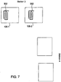
- An example operation using this principle is now illustrated with reference to FIGS. 7 and 8 .
- a first wafer 105-1 and a second wafer 105-2 are rotated from station 2 to station 3. There are no wafers in station 4 at this time.
- the single laser source 102 fires a laser beam on the laser scanners 104 in station 3, which the control system 112 directs to scribe the first half portion 302 on the wafers 105-1 and 105-2. Thereafter, as illustrated in FIG. 8 , the control system 112 rotates the turntable 108 to move the wafers 105-1 and 105-2 into station 4, and a third wafer 105-3 and a fourth wafer 105-4 from station 2 to station 3.
- the single laser source 102 fires a laser beam, which is split into separate beams directed to the laser scanners 104 in both stations 3 and 4.
- the laser scanners 104 in both stations 3 and 4 may be slaved to a single master laser scanner 104, which may be any one of the laser scanners 104.
- the other laser scanners 104 are slaved to the master laser scanner.
- the laser scanners 104 in the station 4 may be configured to move a laser beam in mirror-image relative to the laser scanners 104 in the station 3. This advantageously allows the two half portions of the pattern 301 to be scribed at the same time on different stations using a single laser source 102.
- the first half of the pattern is scribed on a wafer in one station in one firing of the laser source 102, and the second half of the pattern is scribed on the same wafer in another station in a second firing of the laser source 102.
- the scanners 104 in station 3 direct their laser beams to scribe the first half portion 302 on the wafers 105-3 and 105-4.
- the scanners 104 in station 4 direct their laser beams to scribe the second half portion 303 on the wafers 105-1 and 105-2, completing the pattern 301 on those wafers.
- the cycle may be repeated again, allowing for a completed pattern 301 to be scribed on a wafer 105 in two rotary movements of the turntable 108.
- the solar cell ablation system 100 allows for relatively high throughput, i.e., rate of wafer processing, without substantial increase in capital cost.
- the ablation system 100 splits patterning into separate steps performed in different stations in the same firing of the laser source 102. Given that patterning is the slowest part of the system cycle, splitting the pattern formation into several steps reduces the patterning time in a given processing station.
- the ablation system 100 is able to reduce this time to about 7 seconds (a 40% to 50% reduction in patterning time, taking into account overheads) by dividing the patterning into two steps in two different stations.
- the ablation system 100 is advantageous when the duty cycle of a process is greater than 4 seconds and high precision is needed.
- the ablation system 100 provides substantial savings in capital expenditure. Given that the laser source is typically a large portion of the cost of a laser-based ablation system, using a single laser source 102 results in substantial savings. In general, the ablation system 100 reduces redundancy on alignment/calibration cameras, handlers, and lasers.
- the ablation system 100 allows for reduced system complexity.
- the control system 112 controls a single laser source 102 and a single master laser scanner 104.
- the other laser scanners 104 are slaved to the master laser scanner 104. This allows the slaved laser scanners 104 in one station to simply follow the scanning of the master laser scanner 104, and the slaved laser scanners 104 in another station to scan in mirror-image of the master laser scanner 104.
- Mirror-image scanning may be achieved by mirror configuration in the corresponding laser scanner 104 or by taking a complement (or other operation) of the master laser scanner movement, rather than a completely different scanning movement.
- a pattern may require different laser power levels or may have a non-symmetrical design.
- different laser power levels may be required depending on which pattern is being scribed. More specifically, a different laser power level may be needed to form contact holes to a P-type diffusion region as opposed to an N-type diffusion region. The difference in laser power levels may be due to different materials through which the contact holes are formed. In that case, a different laser configuration may be used for each power level or pattern being scribed on the wafer.
- one pattern may be scribed on the wafers in accordance with one laser configuration (e.g., configuration 101-1) in a first step and another pattern may be scribed on the wafers in a second step in accordance with another laser configuration (e.g., 101-2), etc.
- Each of the laser configurations may specify the pattern being scribed and the power level of the laser source scribing that pattern.
- FIG. 9A schematically shows an example pattern 311 to be scribed on a wafer 105 in accordance with an embodiment of the present invention.
- FIG. 9A is not drawn to scale.
- the boundary around the pattern 311 schematically indicates that the pattern 311 is scribed on a wafer 105 using the solar cell ablation system 100.
- the pattern 311 comprises a first pattern 312 and a second pattern 313.
- the pattern 311 is an interdigitated pattern in that the pattern 312 is interdigitated with the pattern 313.
- the pattern 312 may comprise contact holes for a P-type diffusion region and the pattern 313 may comprise contact holes for an N-type diffusion region.
- the portions 312 and 313 may be scribed through different materials. Accordingly, in this example, the pattern 312 may be scribed on a wafer using a laser configuration 101-1 and the pattern 313 may be scribed on the wafer using a laser configuration 101-2.
- the pattern 311 represents a series of contact holes that are not necessarily contiguous or connected. This is exemplified in FIG. 9B where the pattern 312 is depicted as a series of separate dots, with each dot representing a contact hole.
- a first laser configuration may specify a first pattern and a first power level
- a second laser configuration may specify a second pattern and a second power level
- a third laser configuration may specify a third pattern and a third power level
- the first pattern may be the pattern 312 scribed on a wafer at a first power level of the laser source 102
- the second pattern may be the pattern 313 scribed on a wafer at a second power level of the laser source 102.
- the first pattern may be scribed on the wafers at the same time using the first power level on all processing stations in a first rotation of the turntable
- the second pattern may be scribed on the wafers at the same time using the second power level different from the first power level on all processing stations in a second rotation of the turntable, and so on.
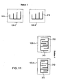
- FIG. 10 An example operation for writing the pattern 311 on a wafer using the ablation system 100 is now explained with reference to FIGS. 10-12 .
- the pattern 312 is scribed on the wafers 105-5 and 105-6 at the same time using a first power level of the laser source 102 in accordance with a laser configuration 101-1. There are no wafers in station 4 of this time.
- the turntable 108 is rotated to move wafers 105-7 and 105-8 into the station 3, and the wafers 105-5 and 105-6 from station 3 to station 4.
- the pattern 313 is scribed on the wafers 105-5, 105-6, 105-7, and 105-8 at the same time at a second power level of the laser source 102 in accordance with a laser configuration 101-2. Note that a complete pattern 311 comprising pattern patterns 312 and 313 is now scribed on the wafers 105-5 and 105-6 (see station 4).
- the turntable is rotated to move wafers 105-9 and 105-10 into the station 3, and the wafers 105-7 and 105-8 from station 3 to station 4.
- the processed wafers 105-5 and 105-6 are moved from station 4 to station 1 (not shown), where the wafers 105-5 and 105-6 are unloaded.
- the pattern 312 is scribed on the wafers 105-7, 105-8, 105-9 and 105-10 at the same time at the first power level of the laser source 102 in accordance with the laser configuration 101-1. Note that the complete pattern 311 comprising patterns 312 and 313 is now scribed on the wafers 105-7 and 105-8 (see station 4). The cycle is repeated with the patterns 313 and 312 being alternately scribed on wafers present on the turntable 108.
- one laser scanner 104 may be designated as the master laser scanner 104. All other laser scanners 104 are slaved to the master. That is, in any given station, only one laser scanner 104 needs to be directly controlled. The other laser scanners 104 may simply follow the master laser scanner 104. Because the patterning steps are independent of one another in this example, the pattern to be scribed on the wafer does not need to be symmetrical. As before, a single laser source 102 may be employed to scribe a complete pattern. This allows for the same benefits as previously explained constrained only by the overhead of switching between laser configurations.
- embodiments of the present invention are not limited to applications involving removal of material from a wafer.
- embodiments of the present invention are equally useful in applications where a laser beam is scanned on a wafer for annealing, diffusion, and other wafer processing steps.
Abstract
A method of processing a wafer, the method comprising: rotating a first wafer from a first station to a second station; in a first scanning step, using a first laser scanner to direct a first laser beam split from a single laser source along a first laser beam path to scan a first pattern on the first wafer in the second station; rotating the first wafer from the second station to a third station; rotating a second wafer from the first station to the second station; and in a second scanning step: using the first laser scanner to direct a second laser beam split from the single laser source along the first laser beam path to scan a second pattern on the second wafer in the second station; and using a second laser scanner to direct a third laser beam split from the single laser source along a second laser beam path to scan the second pattern on the first wafer in the third station, the second laser scanner being slaved to the first laser scanner and scanning the second pattern at substantially the same time as the second pattern is scanned on the second wafer.
Description
- This disclosure was made with Government support under Contract No. DEFC36-07GO17043 awarded by the United States Department of Energy.
- The present invention relates generally to solar cells, and more particularly but not exclusively to solar cell fabrication processes and structures.
- Solar cells are well known devices for converting solar radiation to electrical energy. They may be fabricated on a semiconductor wafer using semiconductor processing technology. A solar cell includes P-type and N-type diffusion regions. Solar radiation impinging on the solar cell creates electrons and holes that migrate to the diffusion regions, thereby creating voltage differentials between the diffusion regions. In a backside contact solar cell, both the diffusion regions and the metal contact fingers coupled to them are on the backside of the solar cell. The metal contact fingers allow an external electrical circuit to be coupled to and be powered by the solar cell.
- To be competitive against other sources of energy, equipment cost and throughput are important considerations in the fabrication of solar cells. Embodiments of the invention pertain to a solar cell ablation system that allows for high throughput while minimizing the cost of the system.
- In one embodiment, a solar cell is formed using a solar cell ablation system. The ablation system includes a single laser source and several laser scanners. The laser scanners include a master laser scanner, with the rest of the laser scanners being slaved to the master laser scanner. A laser beam from the laser source is split into several laser beams, with the laser beams being scanned onto corresponding wafers using the laser scanners in accordance with one or more patterns. The laser beams may be scanned on the wafers using the same or different power levels of the laser source.
- These and other features of the present invention will be readily apparent to persons of ordinary skill in the art upon reading the entirety of this disclosure, which includes the accompanying drawings and claims.
-
-
FIG. 1 is a plan view that schematically shows a solar cell ablation system in accordance with an embodiment of the present invention. -
FIG. 2 is an elevation view of the solar cell ablation system ofFIG. 1 in accordance with an embodiment of the present invention. -
FIGS. 3-5 show cross sections of a wafer undergoing processing to fabricate solar cells in accordance with an embodiment of the present invention. -
FIGS. 6A and 6B schematically show an example pattern to be scribed on a wafer in accordance with an embodiment of the present invention. -
FIGS. 7 and8 illustrate an example operation of a solar cell ablation system in accordance with an embodiment of the present invention. -
FIGS. 9A and 9B schematically show another example pattern to be scribed on a wafer in accordance with an embodiment of the present invention. -
FIGS. 10-12 illustrate another example operation of a solar cell ablation system in accordance with an embodiment of the present invention. - The use of the same reference label in different drawings indicates the same or like components. The drawings are not to scale.
- In the present disclosure, numerous specific details are provided, such as examples of apparatus, process parameters, materials, process steps, and structures, to provide a thorough understanding of embodiments of the invention. Persons of ordinary skill in the art will recognize, however, that the invention can be practiced without one or more of the specific details. In other instances, well-known details are not shown or described to avoid obscuring aspects of the invention.
- The present invention pertains to a high throughput and cost effective solar cell ablation system. Another solar cell ablation system is also disclosed in commonly-assigned
U.S. Patent Application No. 12/795,526, filed on June 7, 2010 -
FIG. 1 is a plan view that schematically shows a solarcell ablation system 100 in accordance with an embodiment of the present invention. In the example ofFIG. 1 , the solarcell ablation system 100 includes aturntable 108, avision system 107, a plurality oflaser scanners 104, asingle laser source 102, and acontrol system 112. Theturntable 108 serves as a workpiece transport for moving solar cell wafers through the different stations of theablation system 100. In some embodiments, different transport mechanisms are used for transporting workpieces between stations. As one non-limiting example, a linear conveyor can be used. In the example ofFIG. 1 , theablation system 100 has four stations namely,stations 1 to 4. Accordingly, theturntable 108 includes fourpositions 109, each having one or more workpiece supports in the form ofchucks 110. Achuck 110 is configured to hold and support a single solar cell wafer. Only some of thechucks 110 are labeled inFIG. 1 to avoid cluttering the figure. Achuck 110 secures the wafer to prevent it from moving while cycling through the stations. -
Station 1 is a load/unload station, where wafers awaiting processing are loaded and processed wafers are unloaded. An automated workpiece handler, such as a pick and place robot, may be used to load and unload wafers to and fromstation 1. Wafers may also be manually loaded and unloaded to and fromstation 1. -
Station 2 includes a workpiece position recognition system for determining the position of a wafer as secured on achuck 110. In the example ofFIG. 1 , the workpiece position recognition system comprises thevision system 107. Thevision system 107 may include a camera and associated processor and software for determining the position of a wafer in aposition 109. Thevision system 107 may compare the position of the wafer relative to a predetermined coordinate system to determine how much the wafer deviates, if any, from an expected position. Thecontrol system 112 may use this deviation information to make an adjustment to the movement of acorresponding laser scanner 104 in directing a laser beam on the wafer. -
Stations cell ablation system 100. Instations FIG. 1 , asingle laser source 102 generates a laser beam that is split into several laser beams, with each of the split laser beams being directed along a laser beam path by acorresponding laser scanner 104 to scan onto a wafer. The laser beam may be split using a beam splitter or other optical/mirror arrangement. The laser beams form contact holes by scribing through materials that have been formed on corresponding wafers. Thelaser source 102 may be a commercially available laser source, such as those available from SPI Lasers and Lumera Laser GmbH. In one embodiment, alaser scanner 104 comprises a galvanometer laser scanner, such as those commercially available from ScanLabs of Germany. - The
control system 112 is electrically coupled to thelaser source 102, thelaser scanners 104, thevision system 107, and the drive of theturntable 108. Thecontrol system 112 controls the operation of the solarcell ablation system 100. More particularly, the control system controls the rotation of theturntable 108, the scanning movement of thelaser scanners 104 to direct laser beams on wafers, and thelaser source 102. In one embodiment, alaser scanner 104 is configured as a master with the rest of thelaser scanners 104 being slaved to the master. The,control system 112 controls the scanning of the master laser scanner, with the rest of the laser scanners following the scanning of the master either exactly or in mirror image depending on the laser configuration. - In an example operation, the
control system 112 drives theturntable 108 to move a wafer fromstation 1 tostation 2. Instation 2, thevision system 107 determines the position of the wafer as held in theposition 109. Thevision system 107 provides the position information to thecontrol system 112, which uses the position information to control the movement of thecorresponding laser scanner 104. Thecontrol system 112 then drives theturntable 108 to move the wafer fromstation 2 tostation 3. There, a laser beam generated by thelaser source 102 removes one or more materials from the wafer in accordance with a pattern and laser power level indicated in a laser configuration 101 that is currently loaded in and employed by thecontrol system 112. Thecontrol system 112 thereafter drives theturntable 108 to move the wafer fromstation 3 tostation 4. As instation 3, a laser beam generated by thelaser source 102 removes one or more materials from the wafer in accordance with the pattern and laser power level indicated in the currently loaded laser configuration 101. Thecontrol system 112 drives theturntable 108 to move the processed wafer fromstation 4 tostation 1, where the processed wafer is unloaded from theablation system 100. As can be appreciated, the solarcell ablation system 100 may be configured to perform different processing steps on wafers being fabricated. That is, the solarcell ablation system 100 may also be used to direct a laser beam on the wafer to perform wafer processing steps other than ablation. -
FIG. 2 is an elevation view of the solarcell ablation system 100 in accordance with an embodiment of the present invention.FIG. 2 shows thevision system 107 instation 2, alaser scanner 104 instation 3, and alaser scanner 104 instation 4. Thestation 1, which is in front of thestation 3, is not shown. Note that there may be more than onelaser scanner 104 in a processing station. Theturntable 108 includes achuck 110 to support awafer 105 in each position. - A turntable approach is employed to avoid redundancy in wafer position recognition (e.g., station 2) or automation stations (e.g., station 1) and to ensure registration between station positions. Stations with low duty cycles are used for all wafers (e.g., load/unload, vision system, automated optical inspection), while only the pattern writing stations (e.g.,
stations 3 and 4) with high duty cycles are repeated in the system hardware. To maximize turntable usage, multiple wafers are processed in each station. The ratio of the number of vision/handling stations compared to the total number of processing stations required may be based on the duty cycles of the stations and physical constraints of the system, such as turntable size, wafer size, etc. As an example, if the turntable is limited to four stations, and the pattern to be scribed is in halves (bi-fold), the total number of vision/handling stations will be half the number of the processing stations. This way, the handling system will be simpler and cheaper, and the vision system will require less cameras. In general, the ablation system may be configured in different ways to maximize throughput while minimizing capital cost for a given cycle time and laser cost. - In the example of
FIG. 1 , the solarcell ablation system 100 has a so-called "4/2/1" design, where the first number indicates the number of rotary table operations or movements, the second number is the number of process stations, and the third number indicates the number of load/unload stations. In the solarcell ablation system 100 ofFIG. 1 , there are four rotary movements, two process stations (stations 3 and 4), and one load/unload station (station 1). Each position of the turntable may have one or more chucks. As can be appreciated, other designs are possible including 3/2/1, 4/3/1, 5/4/1 etc. depending on the application. The design of the ablation system is limited by the physical geometry of the system, the size of the turntable, and number of turns possible. - Alternate embodiments may include combinations of the non-processing stations, such as load/unload, in the same station as the wafer position recognition station, and accepting a slight processing station duty cycle reduction by loading at one station and unloading in another. The embodiment of
FIG. 1 does not include an optical inspection station, but one may be added in another station. Optical inspection may also be incorporated off-line in another tool. - Non-quadrant based approaches may be considered to increase throughput, or to include an automated optical inspection. For example, a turntable that rotates 72 degrees may have 1 station for a vision system, 1 station for load/unload, and 3 process stations, with each of the process stations forming 1/3 of a pattern. As another example, a turntable that rotates 72 degrees may have 1 station for a vision system, 1 station for load/unload, 1 automated optical inspection station, and 2 process stations, with each of the process stations forming 1/2 of a pattern.
-
FIGS. 3-5 show cross sections of awafer 105 undergoing processing to fabricate solar cells in accordance with an embodiment of the present invention. In the example ofFIG. 3 , thewafer 105 includes asolar cell substrate 201 comprising an N-type silicon wafer. Adielectric film stack 210 is formed on alayer 202, which comprises polysilicon in this example. Thefilm stack 210 comprises multiple layers of materials, which in the example ofFIG. 3 include afilm 211, afilm 212, and afilm 213. As shown inFIG. 3 , thefilm 211 may be formed on thefilm 212, which in turn is formed on thefilm 213. In one embodiment, thefilm 211 comprises a layer of silicon nitride formed to a thickness of 300 to 1000 angstroms, thefilm 212 comprises a layer of amorphous silicon formed to a thickness of 30 to 50 angstroms, and thefilm 213 comprises silicon dioxide formed to a thickness of about 120 angstroms. Thefilm 212 may also comprise polysilicon or mc-silicon, depending on the application. - In one embodiment, the
layer 202 comprises polysilicon formed to a thickness of about 2000 angstroms. A P-type diffusion region 203 and an N-type diffusion region 204 are formed in the layer 214. There are several diffusion regions in a solar cell but only one of each conductivity type is shown inFIG. 3 for clarity of illustration. The solar cell ofFIGS. 3-5 is an example of a backside contact solar cell in that thediffusion regions FIG. 5 ), are formed on the backside of the solar cell over the backside of thesubstrate 201. The front side of thewafer 105, which faces the sun to collect solar radiation during normal operation, is opposite the backside. In the example ofFIG. 3 , the front side surface of thesubstrate 201 is textured withrandom pyramids 230. Ananti-reflective layer 231 comprising silicon nitride is formed on the textured surface on the front side. - The
ablation system 100 ofFIG. 1 is employed to ablate thesilicon nitride film 211, theamorphous silicon film 212, and theoxide film 213 to form a hole through them and expose thediffusion regions FIG. 4 , where the ablation step formedcontact holes 220 exposing thediffusion regions metal contacts 221 to be formed in the contact holes 220, as illustrated inFIG. 5 . Themetal contacts 221 allow external electrical circuits to make electrical connection to thediffusion regions - The contact holes 220 may be part of a pattern scribed on a
wafer 105.FIG. 6A schematically shows anexample pattern 301 to be scribed on awafer 105 in accordance with an embodiment of the present invention. As can be appreciated,FIGS. 6A, 6B and the other drawings in this disclosure are not drawn to scale. The boundary around thepattern 301 schematically indicates that thepattern 301 is scribed on awafer 105 using the solarcell ablation system 100. - In the example of
FIG. 6A , thepattern 301 is symmetrical about a dashedline 304. Thepattern 301 comprises afirst half portion 302 and asecond half portion 303. Thepattern 301 is also referred to as "a bi-fold" pattern because thefirst half portion 302 is a mirror image of thesecond half portion 303. Thepattern 301 represents a series of contact holes that are not necessarily contiguous or connected. This is exemplified inFIG. 6B where thefirst half portion 302 is depicted as a series of separate dots, with each dot representing a contact hole. A mirror image pattern, therefore, can be used to refer to such a pattern where the first and second halves are symmetrical about a central axis, including a horizontal or vertical axis. - A laser configuration 101-1 may indicate a pattern of the
pattern 301, and the laser power level and pulse configuration for scribing the half portion on awafer 105. The solarcell ablation system 100 may be configured to use the laser configuration 101-1 to scribe afirst half portion 302 on one wafer and asecond half portion 303 on another wafer at the same time using asingle laser source 102. An example operation using this principle is now illustrated with reference toFIGS. 7 and8 . - In
FIG. 7 , a first wafer 105-1 and a second wafer 105-2 are rotated fromstation 2 tostation 3. There are no wafers instation 4 at this time. Thesingle laser source 102 fires a laser beam on thelaser scanners 104 instation 3, which thecontrol system 112 directs to scribe thefirst half portion 302 on the wafers 105-1 and 105-2. Thereafter, as illustrated inFIG. 8 , thecontrol system 112 rotates theturntable 108 to move the wafers 105-1 and 105-2 intostation 4, and a third wafer 105-3 and a fourth wafer 105-4 fromstation 2 tostation 3. Thesingle laser source 102 fires a laser beam, which is split into separate beams directed to thelaser scanners 104 in bothstations laser scanners 104 in bothstations master laser scanner 104, which may be any one of thelaser scanners 104. Theother laser scanners 104 are slaved to the master laser scanner. Thelaser scanners 104 in thestation 4 may be configured to move a laser beam in mirror-image relative to thelaser scanners 104 in thestation 3. This advantageously allows the two half portions of thepattern 301 to be scribed at the same time on different stations using asingle laser source 102. The first half of the pattern is scribed on a wafer in one station in one firing of thelaser source 102, and the second half of the pattern is scribed on the same wafer in another station in a second firing of thelaser source 102. - Still referring to
FIG. 8 , thescanners 104 instation 3 direct their laser beams to scribe thefirst half portion 302 on the wafers 105-3 and 105-4. At the same time, from the same firing of a laser beam from thelaser source 102, thescanners 104 instation 4 direct their laser beams to scribe thesecond half portion 303 on the wafers 105-1 and 105-2, completing thepattern 301 on those wafers. The cycle may be repeated again, allowing for a completedpattern 301 to be scribed on awafer 105 in two rotary movements of theturntable 108. - As can be appreciated from the foregoing, embodiments of the present invention provide advantages heretofore unrealized. First, the solar
cell ablation system 100 allows for relatively high throughput, i.e., rate of wafer processing, without substantial increase in capital cost. Using asingle laser source 102, theablation system 100 splits patterning into separate steps performed in different stations in the same firing of thelaser source 102. Given that patterning is the slowest part of the system cycle, splitting the pattern formation into several steps reduces the patterning time in a given processing station. For example, assuming forming a complete pattern on a wafer would take 14 seconds, theablation system 100 is able to reduce this time to about 7 seconds (a 40% to 50% reduction in patterning time, taking into account overheads) by dividing the patterning into two steps in two different stations. In general, theablation system 100 is advantageous when the duty cycle of a process is greater than 4 seconds and high precision is needed. - Second, the
ablation system 100 provides substantial savings in capital expenditure. Given that the laser source is typically a large portion of the cost of a laser-based ablation system, using asingle laser source 102 results in substantial savings. In general, theablation system 100 reduces redundancy on alignment/calibration cameras, handlers, and lasers. - Third, the
ablation system 100 allows for reduced system complexity. In theablation system 100, thecontrol system 112 controls asingle laser source 102 and a singlemaster laser scanner 104. Theother laser scanners 104 are slaved to themaster laser scanner 104. This allows the slavedlaser scanners 104 in one station to simply follow the scanning of themaster laser scanner 104, and the slavedlaser scanners 104 in another station to scan in mirror-image of themaster laser scanner 104. Mirror-image scanning may be achieved by mirror configuration in thecorresponding laser scanner 104 or by taking a complement (or other operation) of the master laser scanner movement, rather than a completely different scanning movement. - In some applications, a pattern may require different laser power levels or may have a non-symmetrical design. For example, in interdigitated backside contact solar cells where the materials to the P-type and N-type diffusion regions are different, different laser power levels may be required depending on which pattern is being scribed. More specifically, a different laser power level may be needed to form contact holes to a P-type diffusion region as opposed to an N-type diffusion region. The difference in laser power levels may be due to different materials through which the contact holes are formed. In that case, a different laser configuration may be used for each power level or pattern being scribed on the wafer. Using the solar
cell ablation system 100 ofFIG. 1 as an example, one pattern may be scribed on the wafers in accordance with one laser configuration (e.g., configuration 101-1) in a first step and another pattern may be scribed on the wafers in a second step in accordance with another laser configuration (e.g., 101-2), etc. Each of the laser configurations may specify the pattern being scribed and the power level of the laser source scribing that pattern. -
FIG. 9A schematically shows anexample pattern 311 to be scribed on awafer 105 in accordance with an embodiment of the present invention.FIG. 9A is not drawn to scale. The boundary around thepattern 311 schematically indicates that thepattern 311 is scribed on awafer 105 using the solarcell ablation system 100. - In the example of
FIG. 9A , thepattern 311 comprises afirst pattern 312 and asecond pattern 313. Thepattern 311 is an interdigitated pattern in that thepattern 312 is interdigitated with thepattern 313. Thepattern 312 may comprise contact holes for a P-type diffusion region and thepattern 313 may comprise contact holes for an N-type diffusion region. Theportions pattern 312 may be scribed on a wafer using a laser configuration 101-1 and thepattern 313 may be scribed on the wafer using a laser configuration 101-2. Thepattern 311 represents a series of contact holes that are not necessarily contiguous or connected. This is exemplified inFIG. 9B where thepattern 312 is depicted as a series of separate dots, with each dot representing a contact hole. - In general, a first laser configuration may specify a first pattern and a first power level, a second laser configuration may specify a second pattern and a second power level, a third laser configuration may specify a third pattern and a third power level, and so on. As a particular example, the first pattern may be the
pattern 312 scribed on a wafer at a first power level of thelaser source 102, and the second pattern may be thepattern 313 scribed on a wafer at a second power level of thelaser source 102. - The first pattern may be scribed on the wafers at the same time using the first power level on all processing stations in a first rotation of the turntable, the second pattern may be scribed on the wafers at the same time using the second power level different from the first power level on all processing stations in a second rotation of the turntable, and so on. By alternately using the patterns and corresponding power levels, a completed pattern is scribed in two rotary movements of the turntable.
- An example operation for writing the
pattern 311 on a wafer using theablation system 100 is now explained with reference toFIGS. 10-12 . InFIG. 10 , thepattern 312 is scribed on the wafers 105-5 and 105-6 at the same time using a first power level of thelaser source 102 in accordance with a laser configuration 101-1. There are no wafers instation 4 of this time. - In
FIG. 11 , theturntable 108 is rotated to move wafers 105-7 and 105-8 into thestation 3, and the wafers 105-5 and 105-6 fromstation 3 tostation 4. Thepattern 313 is scribed on the wafers 105-5, 105-6, 105-7, and 105-8 at the same time at a second power level of thelaser source 102 in accordance with a laser configuration 101-2. Note that acomplete pattern 311 comprisingpattern patterns - In
FIG. 12 , the turntable is rotated to move wafers 105-9 and 105-10 into thestation 3, and the wafers 105-7 and 105-8 fromstation 3 tostation 4. In the same rotary movement, the processed wafers 105-5 and 105-6 are moved fromstation 4 to station 1 (not shown), where the wafers 105-5 and 105-6 are unloaded. Thepattern 312 is scribed on the wafers 105-7, 105-8, 105-9 and 105-10 at the same time at the first power level of thelaser source 102 in accordance with the laser configuration 101-1. Note that thecomplete pattern 311 comprisingpatterns patterns turntable 108. - In the example of
FIGS. 10-12 , onelaser scanner 104 may be designated as themaster laser scanner 104. Allother laser scanners 104 are slaved to the master. That is, in any given station, only onelaser scanner 104 needs to be directly controlled. Theother laser scanners 104 may simply follow themaster laser scanner 104. Because the patterning steps are independent of one another in this example, the pattern to be scribed on the wafer does not need to be symmetrical. As before, asingle laser source 102 may be employed to scribe a complete pattern. This allows for the same benefits as previously explained constrained only by the overhead of switching between laser configurations. - As can be appreciated from the foregoing, embodiments of the present invention are not limited to applications involving removal of material from a wafer. For example, embodiments of the present invention are equally useful in applications where a laser beam is scanned on a wafer for annealing, diffusion, and other wafer processing steps.
- A high throughput solar cell ablation system has been disclosed. While specific embodiments of the present invention have been provided, it is to be understood that these embodiments are for illustration purposes and not limiting. Many additional embodiments will be apparent to persons of ordinary skill in the art reading this disclosure.
-
- 1. A method of fabricating a solar cell, the method comprising:
- generating a laser beam from a single laser source;
- splitting the laser beam along a first laser beam path and a second laser beam path;
- in a first scanning step, directing the laser beam along the first laser beam path to scan on the first wafer in the first station in accordance with a first pattern;
- moving the first wafer from the first station to a second station, and a second wafer to the first station;
- in a second scanning step after the first scanning step and after moving the first and second wafers, directing the laser beam along the second laser beam path to scan on the first wafer in the second station in accordance with a second pattern, the second pattern being a mirror image of the first pattern, and directing the laser beam along the first laser beam path to scan on the second wafer in accordance with the first pattern, the scanning on the first and second wafers being performed substantially simultaneously.
- 2. The method of
embodiment 1 wherein the first and second patterns form contact holes that exposes a diffusion region of a solar cell being fabricated on the wafer, and further comprising forming a metal contact into the contact hole to electrically connect to the diffusion region. - 3. The method of
embodiment 1 wherein, during the second scanning step, directing the laser beam on to the first wafer is performed using a first of a plurality of laser scanners that is slaved to a master laser scanner, wherein the master laser scanner is used to direct the laser beam on to the second wafer. - 4. The method of
embodiment 3 wherein the plurality of laser scanners and the master laser scanner comprise galvanometer laser scanners. - 5. The method of
embodiment 1, further comprising:- moving the first wafer from the second station, the second wafer from the first station to the second station, and a third wafer to the first station;
- in a third scanning step after the second scanning step, and after moving the first, second, and third wafers, directing the laser beam along the second laser beam path to scan on the second wafer in the second station in accordance with the second pattern and directing the laser beam along the first laser beam path to scan on the third wafer in accordance with the first pattern, the scanning on the second and third wafers being performed substantially simultaneously.
- 6. The method of
embodiment 1, wherein moving the first wafer comprises rotating a turntable supporting the first wafer. - 7. A wafer processing system comprising:
- a plurality of stations;
- a turntable having a position for each of the plurality of stations, the position being configured to support a plurality of wafers;
- a single laser source;
- a beam splitter adapted to split a main laser beam from the single laser source into a first laser beam and a second laser beam;
- a master laser scanner adapted to direct the first laser beam to scan on to a first of the plurality of wafers in accordance with a first pattern;
- a slave laser scanner adapted to be controlled by the master laser scanner and to direct the second laser beam to scan on to a second of the plurality of wafers in accordance with a second pattern, the second pattern being a mirror image of the first pattern, at substantially the same time as the scanning of the first laser beam on to the first of the plurality of wafers by the master laser scanner.
- 8. The system of embodiment 7 wherein the slave laser scanner comprises a galvanometer laser scanner.
- 9. The system of embodiment 7 wherein the first pattern is scanned on to the first of the plurality of wafers and the second pattern is scanned on to the second of the plurality of wafers at the same power level of the single laser source.
- 10. The system of embodiment 7 further comprising a vision system in a station in the plurality of stations, the vision system being configured to recognize a position of the plurality of wafers on the turntable.
- 11. The system of embodiment 7 further comprising a station in the plurality of stations where the plurality of wafers is loaded onto the turntable.
- 12. The system of embodiment 7 wherein the first pattern and the second pattern are scribed at a same power level of the single laser source.
- 13. A method of processing a wafer, the method comprising:
- rotating a first wafer from a first station to a second station;
- in a first scanning step, using a first laser scanner to direct a first laser beam split from a single laser source along a first laser beam path to scan a first pattern on the first wafer in the second station;
- rotating the first wafer from the second station to a third station;
- rotating a second wafer from the first station to the second station; and
- in a second scanning step:
- using the first laser scanner to direct a second laser beam split from the single laser source along the first laser beam path to scan a second pattern on the second wafer in the second station; and
- using a second laser scanner to direct a third laser beam split from the single laser source along a second laser beam path to scan the second pattern on the first wafer in the third station, the second laser scanner being slaved to the first laser scanner and scanning the second pattern at substantially the same time as the second pattern is scanned on the second wafer.
- 14. The method of embodiment 13 wherein the first pattern is scanned at a first power level and the second pattern is scanned at a second power level.
- 15. The method of embodiment 14 wherein the first and second power levels are different.
- 16. The method of embodiment 13 wherein the first pattern is different than the second pattern.
- 17. The method of embodiment 16 wherein the first and second patterns are not symmetrical.
- 18. The method of embodiment 13, further comprising:
- rotating the first wafer from the third station;
- rotating the second wafer from the second station to the third station; and
- in a third scanning step:
- using the first laser scanner to direct a fourth laser beam split from the single laser source along the first laser beam path to scan the first pattern on the third wafer in the second station; and
Claims (6)
- A method of processing a wafer, the method comprising:rotating a first wafer from a first station to a second station;in a first scanning step, using a first laser scanner to direct a first laser beam split from a single laser source along a first laser beam path to scan a first pattern on the first wafer in the second station;rotating the first wafer from the second station to a third station;rotating a second wafer from the first station to the second station; andin a second scanning step:using the first laser scanner to direct a second laser beam split from the single laser source along the first laser beam path to scan a second pattern on the second wafer in the second station; andusing a second laser scanner to direct a third laser beam split from the single laser source along a second laser beam path to scan the second pattern on the first wafer in the third station, the second laser scanner being slaved to the first laser scanner and scanning the second pattern at substantially the same time as the second pattern is scanned on the second wafer.
- The method of claim 1 wherein the first pattern is scanned at a first power level and the second pattern is scanned at a second power level.
- The method of claim 2 wherein the first and second power levels are different.
- The method of claim 1 wherein the first pattern is different than the second pattern.
- The method of claim 4 wherein the first and second patterns are not symmetrical.
- The method of claim 1, further comprising:rotating the first wafer from the third station;rotating the second wafer from the second station to the third station; andin a third scanning step:using the first laser scanner to direct a fourth laser beam split from the single laser source along the first laser beam path to scan the first pattern on the third wafer in the second station; andusing the second laser scanner to direct a fifth laser beam split from the single laser source along the second laser beam path to scan the first pattern on the second wafer in the third station at substantially the same time as the first pattern is scanned on the third wafer.
Applications Claiming Priority (2)
| Application Number | Priority Date | Filing Date | Title |
|---|---|---|---|
| US12/829,275 US8263899B2 (en) | 2010-07-01 | 2010-07-01 | High throughput solar cell ablation system |
| EP11801292.1A EP2588267B1 (en) | 2010-07-01 | 2011-04-25 | High throughput solar cell ablation system |
Related Parent Applications (2)
| Application Number | Title | Priority Date | Filing Date |
|---|---|---|---|
| EP11801292.1A Division-Into EP2588267B1 (en) | 2010-07-01 | 2011-04-25 | High throughput solar cell ablation system |
| EP11801292.1A Division EP2588267B1 (en) | 2010-07-01 | 2011-04-25 | High throughput solar cell ablation system |
Publications (1)
| Publication Number | Publication Date |
|---|---|
| EP3299109A1 true EP3299109A1 (en) | 2018-03-28 |
Family
ID=45400014
Family Applications (2)
| Application Number | Title | Priority Date | Filing Date |
|---|---|---|---|
| EP17197554.3A Withdrawn EP3299109A1 (en) | 2010-07-01 | 2011-04-25 | High throughput solar cell ablation system |
| EP11801292.1A Active EP2588267B1 (en) | 2010-07-01 | 2011-04-25 | High throughput solar cell ablation system |
Family Applications After (1)
| Application Number | Title | Priority Date | Filing Date |
|---|---|---|---|
| EP11801292.1A Active EP2588267B1 (en) | 2010-07-01 | 2011-04-25 | High throughput solar cell ablation system |
Country Status (6)
| Country | Link |
|---|---|
| US (3) | US8263899B2 (en) |
| EP (2) | EP3299109A1 (en) |
| JP (2) | JP6318419B2 (en) |
| KR (1) | KR101775491B1 (en) |
| CN (1) | CN102985213B (en) |
| WO (1) | WO2012003033A1 (en) |
Families Citing this family (26)
| Publication number | Priority date | Publication date | Assignee | Title |
|---|---|---|---|---|
| US8263899B2 (en) * | 2010-07-01 | 2012-09-11 | Sunpower Corporation | High throughput solar cell ablation system |
| US8692111B2 (en) * | 2011-08-23 | 2014-04-08 | Sunpower Corporation | High throughput laser ablation processes and structures for forming contact holes in solar cells |
| KR101466669B1 (en) * | 2013-05-31 | 2014-12-01 | 주식회사 엘티에스 | Apparatus for manufacturing through-hole of tempered glass cell |
| US20160284921A1 (en) * | 2013-10-30 | 2016-09-29 | Kyocera Corporation | Light receiving/emitting element and sensor device using same |
| CN106583932A (en) * | 2014-06-10 | 2017-04-26 | 赵牧青 | Economical laser marking system with material discharging manipulator |
| US20160158890A1 (en) * | 2014-12-05 | 2016-06-09 | Solarcity Corporation | Systems and methods for scribing photovoltaic structures |
| US9899546B2 (en) | 2014-12-05 | 2018-02-20 | Tesla, Inc. | Photovoltaic cells with electrodes adapted to house conductive paste |
| US9786562B2 (en) * | 2015-04-21 | 2017-10-10 | Asm Technology Singapore Pte Ltd | Method and device for cutting wafers |
| JP6552948B2 (en) * | 2015-11-27 | 2019-07-31 | 株式会社ディスコ | Wafer processing method and processing apparatus |
| EP3206233A1 (en) * | 2016-02-12 | 2017-08-16 | Lg Electronics Inc. | Solar cell and method of manufacturing the same |
| USD822890S1 (en) | 2016-09-07 | 2018-07-10 | Felxtronics Ap, Llc | Lighting apparatus |
| US10775030B2 (en) | 2017-05-05 | 2020-09-15 | Flex Ltd. | Light fixture device including rotatable light modules |
| USD832494S1 (en) | 2017-08-09 | 2018-10-30 | Flex Ltd. | Lighting module heatsink |
| USD833061S1 (en) | 2017-08-09 | 2018-11-06 | Flex Ltd. | Lighting module locking endcap |
| USD846793S1 (en) | 2017-08-09 | 2019-04-23 | Flex Ltd. | Lighting module locking mechanism |
| USD872319S1 (en) | 2017-08-09 | 2020-01-07 | Flex Ltd. | Lighting module LED light board |
| USD877964S1 (en) | 2017-08-09 | 2020-03-10 | Flex Ltd. | Lighting module |
| USD862777S1 (en) | 2017-08-09 | 2019-10-08 | Flex Ltd. | Lighting module wide distribution lens |
| USD832495S1 (en) | 2017-08-18 | 2018-10-30 | Flex Ltd. | Lighting module locking mechanism |
| USD862778S1 (en) | 2017-08-22 | 2019-10-08 | Flex Ltd | Lighting module lens |
| USD888323S1 (en) | 2017-09-07 | 2020-06-23 | Flex Ltd | Lighting module wire guard |
| KR20190133502A (en) * | 2018-05-23 | 2019-12-03 | 한화정밀기계 주식회사 | Processing device for wafer |
| DE102018119313B4 (en) * | 2018-08-08 | 2023-03-30 | Rogers Germany Gmbh | Process for processing a metal-ceramic substrate and installation for carrying out the process |
| JP7402814B2 (en) * | 2018-10-30 | 2023-12-21 | 浜松ホトニクス株式会社 | Laser processing head and laser processing equipment |
| CN112955274B (en) * | 2018-10-30 | 2023-11-07 | 浜松光子学株式会社 | Laser processing device |
| US20210276129A1 (en) * | 2020-03-09 | 2021-09-09 | Applied Materials, Inc. | Laser dicing system for filamenting and singulating optical devices |
Citations (7)
| Publication number | Priority date | Publication date | Assignee | Title |
|---|---|---|---|---|
| US4443685A (en) * | 1982-02-17 | 1984-04-17 | Westinghouse Electric Corp. | Fixture for laser scribing (of dendrite silicon cells) |
| JP2005074479A (en) * | 2003-09-01 | 2005-03-24 | Sumitomo Heavy Ind Ltd | Laser beam machining device and laser beam machining method |
| WO2008038385A1 (en) * | 2006-09-28 | 2008-04-03 | Mitsubishi Electric Corporation | Laser working apparatus |
| EP1925964A1 (en) * | 2006-11-21 | 2008-05-28 | Palo Alto Research Center Incorporated | Light scanning mechanism for scan displacement invariant laser ablation apparatus |
| JP2009226445A (en) * | 2008-03-24 | 2009-10-08 | Miyachi Technos Corp | Scanning type laser beam machining apparatus |
| WO2010037346A1 (en) * | 2008-10-05 | 2010-04-08 | Changzhou Lasfocus Laser Equipment Co., Ltd. | Methods and systems of manufacturing photovoltaic devices |
| US20100147811A1 (en) * | 2008-12-11 | 2010-06-17 | Sobey Mark S | Apparatus for laser scribing of dielectric-coated semiconductor wafers |
Family Cites Families (66)
| Publication number | Priority date | Publication date | Assignee | Title |
|---|---|---|---|---|
| US4322571A (en) | 1980-07-17 | 1982-03-30 | The Boeing Company | Solar cells and methods for manufacture thereof |
| US4626613A (en) | 1983-12-23 | 1986-12-02 | Unisearch Limited | Laser grooved solar cell |
| US4796038A (en) * | 1985-07-24 | 1989-01-03 | Ateq Corporation | Laser pattern generation apparatus |
| US5011565A (en) | 1989-12-06 | 1991-04-30 | Mobil Solar Energy Corporation | Dotted contact solar cell and method of making same |
| JP2798769B2 (en) | 1990-02-22 | 1998-09-17 | 三洋電機株式会社 | Method for manufacturing thin film transistor |
| US5258077A (en) | 1991-09-13 | 1993-11-02 | Solec International, Inc. | High efficiency silicon solar cells and method of fabrication |
| US5432015A (en) | 1992-05-08 | 1995-07-11 | Westaim Technologies, Inc. | Electroluminescent laminate with thick film dielectric |
| US5738731A (en) | 1993-11-19 | 1998-04-14 | Mega Chips Corporation | Photovoltaic device |
| US5456763A (en) | 1994-03-29 | 1995-10-10 | The Regents Of The University Of California | Solar cells utilizing pulsed-energy crystallized microcrystalline/polycrystalline silicon |
| KR0165423B1 (en) | 1995-07-24 | 1998-12-15 | 김광호 | Interconnection structure of semiconductor device and its manufacture |
| US5635086A (en) * | 1995-10-10 | 1997-06-03 | The Esab Group, Inc. | Laser-plasma arc metal cutting apparatus |
| US5916461A (en) * | 1997-02-19 | 1999-06-29 | Technolines, Llc | System and method for processing surfaces by a laser |
| DE19741832A1 (en) | 1997-09-23 | 1999-03-25 | Inst Solarenergieforschung | Method of manufacturing a solar cell and solar cell |
| US6185030B1 (en) * | 1998-03-20 | 2001-02-06 | James W. Overbeck | Wide field of view and high speed scanning microscopy |
| US6924493B1 (en) * | 1999-08-17 | 2005-08-02 | The Regents Of The University Of California | Ion beam lithography system |
| US7838794B2 (en) | 1999-12-28 | 2010-11-23 | Gsi Group Corporation | Laser-based method and system for removing one or more target link structures |
| DE10046170A1 (en) | 2000-09-19 | 2002-04-04 | Fraunhofer Ges Forschung | Method for producing a semiconductor-metal contact through a dielectric layer |
| US20070128827A1 (en) * | 2001-09-12 | 2007-06-07 | Faris Sadeg M | Method and system for increasing yield of vertically integrated devices |
| US7420147B2 (en) * | 2001-09-12 | 2008-09-02 | Reveo, Inc. | Microchannel plate and method of manufacturing microchannel plate |
| US6697096B2 (en) * | 2001-11-16 | 2004-02-24 | Applied Materials, Inc. | Laser beam pattern generator having rotating scanner compensator and method |
| DE60332406D1 (en) * | 2002-03-15 | 2010-06-17 | Affymetrix Inc | System and method for scanning biological materials |
| JP4363029B2 (en) | 2002-11-06 | 2009-11-11 | ソニー株式会社 | Manufacturing method of split wave plate filter |
| US20060060238A1 (en) | 2004-02-05 | 2006-03-23 | Advent Solar, Inc. | Process and fabrication methods for emitter wrap through back contact solar cells |
| US20060000814A1 (en) * | 2004-06-30 | 2006-01-05 | Bo Gu | Laser-based method and system for processing targeted surface material and article produced thereby |
| US7164465B2 (en) * | 2004-07-13 | 2007-01-16 | Anvik Corporation | Versatile maskless lithography system with multiple resolutions |
| DE102004050269A1 (en) | 2004-10-14 | 2006-04-20 | Institut Für Solarenergieforschung Gmbh | Process for the contact separation of electrically conductive layers on back-contacted solar cells and solar cell |
| US20090107545A1 (en) | 2006-10-09 | 2009-04-30 | Soltaix, Inc. | Template for pyramidal three-dimensional thin-film solar cell manufacturing and methods of use |
| US9508886B2 (en) * | 2007-10-06 | 2016-11-29 | Solexel, Inc. | Method for making a crystalline silicon solar cell substrate utilizing flat top laser beam |
| US8399331B2 (en) | 2007-10-06 | 2013-03-19 | Solexel | Laser processing for high-efficiency thin crystalline silicon solar cell fabrication |
| US8129822B2 (en) | 2006-10-09 | 2012-03-06 | Solexel, Inc. | Template for three-dimensional thin-film solar cell manufacturing and methods of use |
| US8420435B2 (en) | 2009-05-05 | 2013-04-16 | Solexel, Inc. | Ion implantation fabrication process for thin-film crystalline silicon solar cells |
| US7554031B2 (en) | 2005-03-03 | 2009-06-30 | Sunpower Corporation | Preventing harmful polarization of solar cells |
| US20070169806A1 (en) | 2006-01-20 | 2007-07-26 | Palo Alto Research Center Incorporated | Solar cell production using non-contact patterning and direct-write metallization |
| US20070137692A1 (en) | 2005-12-16 | 2007-06-21 | Bp Corporation North America Inc. | Back-Contact Photovoltaic Cells |
| US7834293B2 (en) * | 2006-05-02 | 2010-11-16 | Electro Scientific Industries, Inc. | Method and apparatus for laser processing |
| US7759607B2 (en) | 2006-06-20 | 2010-07-20 | Optical Analytics, Inc. | Method of direct Coulomb explosion in laser ablation of semiconductor structures |
| DE102006028718B4 (en) | 2006-06-20 | 2008-11-13 | Infineon Technologies Ag | Method for separating semiconductor wafers into semiconductor chips |
| TWI328877B (en) | 2006-07-20 | 2010-08-11 | Au Optronics Corp | Array substrate |
| US20080116182A1 (en) * | 2006-11-21 | 2008-05-22 | Palo Alto Research Center Incorporated | Multiple Station Scan Displacement Invariant Laser Ablation Apparatus |
| US7732104B2 (en) | 2007-01-18 | 2010-06-08 | International Business Machines Corporation | System and method for eliminating the structure and edge roughness produced during laser ablation of a material |
| US20080202577A1 (en) * | 2007-02-16 | 2008-08-28 | Henry Hieslmair | Dynamic design of solar cell structures, photovoltaic modules and corresponding processes |
| TWI328861B (en) | 2007-03-13 | 2010-08-11 | Au Optronics Corp | Fabrication methods of thin film transistor substrate |
| JP2008227379A (en) * | 2007-03-15 | 2008-09-25 | Keyence Corp | Laser beam machine and solid-state laser resonator |
| US8536483B2 (en) * | 2007-03-22 | 2013-09-17 | General Lasertronics Corporation | Methods for stripping and modifying surfaces with laser-induced ablation |
| JP2008283023A (en) | 2007-05-11 | 2008-11-20 | Mitsubishi Heavy Ind Ltd | Production process of photoelectric conversion device |
| US7838062B2 (en) | 2007-05-29 | 2010-11-23 | Sunpower Corporation | Array of small contacts for solar cell fabrication |
| JP4916392B2 (en) * | 2007-06-26 | 2012-04-11 | パナソニック株式会社 | Manufacturing method and manufacturing apparatus for three-dimensional shaped object |
| JP5230153B2 (en) | 2007-09-18 | 2013-07-10 | 三菱重工業株式会社 | Method for manufacturing photoelectric conversion device |
| US8198528B2 (en) | 2007-12-14 | 2012-06-12 | Sunpower Corporation | Anti-reflective coating with high optical absorption layer for backside contact solar cells |
| US20090188553A1 (en) | 2008-01-25 | 2009-07-30 | Emat Technology, Llc | Methods of fabricating solar-cell structures and resulting solar-cell structures |
| US7989729B1 (en) * | 2008-03-11 | 2011-08-02 | Kla-Tencor Corporation | Detecting and repairing defects of photovoltaic devices |
| US7833808B2 (en) | 2008-03-24 | 2010-11-16 | Palo Alto Research Center Incorporated | Methods for forming multiple-layer electrode structures for silicon photovoltaic cells |
| US7851698B2 (en) | 2008-06-12 | 2010-12-14 | Sunpower Corporation | Trench process and structure for backside contact solar cells with polysilicon doped regions |
| CN102131950B (en) * | 2008-06-19 | 2014-05-28 | 实用光有限公司 | Light induced patterning |
| CN103537811A (en) * | 2008-08-26 | 2014-01-29 | 应用材料公司 | Laser material removal methods and apparatus |
| US7855089B2 (en) | 2008-09-10 | 2010-12-21 | Stion Corporation | Application specific solar cell and method for manufacture using thin film photovoltaic materials |
| CN102217056A (en) * | 2008-11-19 | 2011-10-12 | 应用材料股份有限公司 | Laser-scribing tool architecture |
| JP5381052B2 (en) * | 2008-12-01 | 2014-01-08 | 富士通セミコンダクター株式会社 | Semiconductor device and method for manufacturing semiconductor integrated circuit chip |
| JP5318545B2 (en) * | 2008-12-01 | 2013-10-16 | 株式会社ディスコ | Wafer processing method |
| CN102439728B (en) | 2009-04-21 | 2015-08-19 | 泰特拉桑有限公司 | Form the method for the structure in solar cell |
| EP2422377A4 (en) | 2009-04-22 | 2013-12-04 | Tetrasun Inc | Localized metal contacts by localized laser assisted conversion of functional films in solar cells |
| WO2011041267A2 (en) * | 2009-09-29 | 2011-04-07 | Applied Materials, Inc. | Laser system for processing solar wafers in a carrier |
| US20110216401A1 (en) * | 2010-03-03 | 2011-09-08 | Palo Alto Research Center Incorporated | Scanning System With Orbiting Objective |
| US8211731B2 (en) | 2010-06-07 | 2012-07-03 | Sunpower Corporation | Ablation of film stacks in solar cell fabrication processes |
| US8263899B2 (en) * | 2010-07-01 | 2012-09-11 | Sunpower Corporation | High throughput solar cell ablation system |
| EP2601687A4 (en) * | 2010-08-05 | 2018-03-07 | Solexel, Inc. | Backplane reinforcement and interconnects for solar cells |
-
2010
- 2010-07-01 US US12/829,275 patent/US8263899B2/en active Active
-
2011
- 2011-04-25 KR KR1020137000215A patent/KR101775491B1/en active IP Right Grant
- 2011-04-25 CN CN201180032547.4A patent/CN102985213B/en active Active
- 2011-04-25 WO PCT/US2011/033764 patent/WO2012003033A1/en active Application Filing
- 2011-04-25 EP EP17197554.3A patent/EP3299109A1/en not_active Withdrawn
- 2011-04-25 EP EP11801292.1A patent/EP2588267B1/en active Active
- 2011-04-25 JP JP2013518384A patent/JP6318419B2/en active Active
-
2012
- 2012-08-13 US US13/584,613 patent/US8859933B2/en active Active
-
2014
- 2014-09-19 US US14/491,662 patent/US9527164B2/en active Active
-
2016
- 2016-05-02 JP JP2016092823A patent/JP6216407B2/en active Active
Patent Citations (7)
| Publication number | Priority date | Publication date | Assignee | Title |
|---|---|---|---|---|
| US4443685A (en) * | 1982-02-17 | 1984-04-17 | Westinghouse Electric Corp. | Fixture for laser scribing (of dendrite silicon cells) |
| JP2005074479A (en) * | 2003-09-01 | 2005-03-24 | Sumitomo Heavy Ind Ltd | Laser beam machining device and laser beam machining method |
| WO2008038385A1 (en) * | 2006-09-28 | 2008-04-03 | Mitsubishi Electric Corporation | Laser working apparatus |
| EP1925964A1 (en) * | 2006-11-21 | 2008-05-28 | Palo Alto Research Center Incorporated | Light scanning mechanism for scan displacement invariant laser ablation apparatus |
| JP2009226445A (en) * | 2008-03-24 | 2009-10-08 | Miyachi Technos Corp | Scanning type laser beam machining apparatus |
| WO2010037346A1 (en) * | 2008-10-05 | 2010-04-08 | Changzhou Lasfocus Laser Equipment Co., Ltd. | Methods and systems of manufacturing photovoltaic devices |
| US20100147811A1 (en) * | 2008-12-11 | 2010-06-17 | Sobey Mark S | Apparatus for laser scribing of dielectric-coated semiconductor wafers |
Also Published As
| Publication number | Publication date |
|---|---|
| US20150108692A1 (en) | 2015-04-23 |
| KR20130121073A (en) | 2013-11-05 |
| US20120003788A1 (en) | 2012-01-05 |
| US8263899B2 (en) | 2012-09-11 |
| CN102985213B (en) | 2015-12-02 |
| US8859933B2 (en) | 2014-10-14 |
| KR101775491B1 (en) | 2017-09-06 |
| EP2588267B1 (en) | 2017-12-13 |
| JP6216407B2 (en) | 2017-10-18 |
| WO2012003033A1 (en) | 2012-01-05 |
| EP2588267A1 (en) | 2013-05-08 |
| JP2016165758A (en) | 2016-09-15 |
| US20120312791A1 (en) | 2012-12-13 |
| EP2588267A4 (en) | 2015-12-02 |
| US9527164B2 (en) | 2016-12-27 |
| CN102985213A (en) | 2013-03-20 |
| JP6318419B2 (en) | 2018-05-09 |
| JP2013536080A (en) | 2013-09-19 |
Similar Documents
| Publication | Publication Date | Title |
|---|---|---|
| EP2588267B1 (en) | High throughput solar cell ablation system | |
| US8569650B2 (en) | Laser material removal methods and apparatus | |
| EP1926150B1 (en) | Multiple station laser ablation apparatus | |
| US20110076847A1 (en) | Laser system for processing solar wafers in a carrier | |
| KR20110020272A (en) | Next generation screen printing system | |
| US8021913B2 (en) | Method and apparatus for forming the separating lines of a photovoltaic module with series-connected cells | |
| US20100147811A1 (en) | Apparatus for laser scribing of dielectric-coated semiconductor wafers | |
| JP4713100B2 (en) | Method for manufacturing photoelectric conversion device and photoelectric conversion device | |
| JP2006041322A5 (en) | ||
| JP2010279969A (en) | Laser beam machining method, laser beam machining apparatus and method of manufacturing solar panel | |
| Harley et al. | High throughput laser processing | |
| Harley et al. | High throughput solar cell ablation system | |
| KR101390423B1 (en) | Method and apparatus for laser manufacturing of simultaneous manufacturing type | |
| WO2018127295A1 (en) | Apparatus for processing of substrates used in the manufacture of solar cells, system for the manufacture of solar cells, and method for processing of substrates used in the manufacture of solar cells | |
| KR101290106B1 (en) | Method for manufacturing solar cell using laser | |
| WO2022174904A1 (en) | Transportation system for transporting two or more substrates, printing apparatus for printing on two or more substrates, and methods for performing same | |
| KR20110120478A (en) | Method for manufacturing thin-film type solar cell and laser machining device |
Legal Events
| Date | Code | Title | Description |
|---|---|---|---|
| PUAI | Public reference made under article 153(3) epc to a published international application that has entered the european phase |
Free format text: ORIGINAL CODE: 0009012 |
|
| AC | Divisional application: reference to earlier application |
Ref document number: 2588267 Country of ref document: EP Kind code of ref document: P |
|
| AK | Designated contracting states |
Kind code of ref document: A1 Designated state(s): AL AT BE BG CH CY CZ DE DK EE ES FI FR GB GR HR HU IE IS IT LI LT LU LV MC MK MT NL NO PL PT RO RS SE SI SK SM TR |
|
| STAA | Information on the status of an ep patent application or granted ep patent |
Free format text: STATUS: THE APPLICATION IS DEEMED TO BE WITHDRAWN |
|
| 18D | Application deemed to be withdrawn |
Effective date: 20180929 |