EP3297105A1 - Driver circuit for a laser diode - Google Patents
Driver circuit for a laser diode Download PDFInfo
- Publication number
- EP3297105A1 EP3297105A1 EP16189306.0A EP16189306A EP3297105A1 EP 3297105 A1 EP3297105 A1 EP 3297105A1 EP 16189306 A EP16189306 A EP 16189306A EP 3297105 A1 EP3297105 A1 EP 3297105A1
- Authority
- EP
- European Patent Office
- Prior art keywords
- laser diode
- current
- input
- driver circuit
- voltage
- Prior art date
- Legal status (The legal status is an assumption and is not a legal conclusion. Google has not performed a legal analysis and makes no representation as to the accuracy of the status listed.)
- Granted
Links
Images


Classifications
-
- H—ELECTRICITY
- H01—ELECTRIC ELEMENTS
- H01S—DEVICES USING THE PROCESS OF LIGHT AMPLIFICATION BY STIMULATED EMISSION OF RADIATION [LASER] TO AMPLIFY OR GENERATE LIGHT; DEVICES USING STIMULATED EMISSION OF ELECTROMAGNETIC RADIATION IN WAVE RANGES OTHER THAN OPTICAL
- H01S5/00—Semiconductor lasers
- H01S5/04—Processes or apparatus for excitation, e.g. pumping, e.g. by electron beams
- H01S5/042—Electrical excitation ; Circuits therefor
- H01S5/0428—Electrical excitation ; Circuits therefor for applying pulses to the laser
-
- H—ELECTRICITY
- H01—ELECTRIC ELEMENTS
- H01S—DEVICES USING THE PROCESS OF LIGHT AMPLIFICATION BY STIMULATED EMISSION OF RADIATION [LASER] TO AMPLIFY OR GENERATE LIGHT; DEVICES USING STIMULATED EMISSION OF ELECTROMAGNETIC RADIATION IN WAVE RANGES OTHER THAN OPTICAL
- H01S5/00—Semiconductor lasers
- H01S5/04—Processes or apparatus for excitation, e.g. pumping, e.g. by electron beams
- H01S5/042—Electrical excitation ; Circuits therefor
-
- H—ELECTRICITY
- H01—ELECTRIC ELEMENTS
- H01S—DEVICES USING THE PROCESS OF LIGHT AMPLIFICATION BY STIMULATED EMISSION OF RADIATION [LASER] TO AMPLIFY OR GENERATE LIGHT; DEVICES USING STIMULATED EMISSION OF ELECTROMAGNETIC RADIATION IN WAVE RANGES OTHER THAN OPTICAL
- H01S5/00—Semiconductor lasers
- H01S5/02—Structural details or components not essential to laser action
- H01S5/026—Monolithically integrated components, e.g. waveguides, monitoring photo-detectors, drivers
- H01S5/0261—Non-optical elements, e.g. laser driver components, heaters
-
- H—ELECTRICITY
- H01—ELECTRIC ELEMENTS
- H01S—DEVICES USING THE PROCESS OF LIGHT AMPLIFICATION BY STIMULATED EMISSION OF RADIATION [LASER] TO AMPLIFY OR GENERATE LIGHT; DEVICES USING STIMULATED EMISSION OF ELECTROMAGNETIC RADIATION IN WAVE RANGES OTHER THAN OPTICAL
- H01S5/00—Semiconductor lasers
- H01S5/10—Construction or shape of the optical resonator, e.g. extended or external cavity, coupled cavities, bent-guide, varying width, thickness or composition of the active region
- H01S5/18—Surface-emitting [SE] lasers, e.g. having both horizontal and vertical cavities
- H01S5/183—Surface-emitting [SE] lasers, e.g. having both horizontal and vertical cavities having only vertical cavities, e.g. vertical cavity surface-emitting lasers [VCSEL]
-
- H—ELECTRICITY
- H05—ELECTRIC TECHNIQUES NOT OTHERWISE PROVIDED FOR
- H05B—ELECTRIC HEATING; ELECTRIC LIGHT SOURCES NOT OTHERWISE PROVIDED FOR; CIRCUIT ARRANGEMENTS FOR ELECTRIC LIGHT SOURCES, IN GENERAL
- H05B45/00—Circuit arrangements for operating light-emitting diodes [LED]
- H05B45/40—Details of LED load circuits
- H05B45/44—Details of LED load circuits with an active control inside an LED matrix
- H05B45/48—Details of LED load circuits with an active control inside an LED matrix having LEDs organised in strings and incorporating parallel shunting devices
-
- H—ELECTRICITY
- H01—ELECTRIC ELEMENTS
- H01S—DEVICES USING THE PROCESS OF LIGHT AMPLIFICATION BY STIMULATED EMISSION OF RADIATION [LASER] TO AMPLIFY OR GENERATE LIGHT; DEVICES USING STIMULATED EMISSION OF ELECTROMAGNETIC RADIATION IN WAVE RANGES OTHER THAN OPTICAL
- H01S5/00—Semiconductor lasers
- H01S5/06—Arrangements for controlling the laser output parameters, e.g. by operating on the active medium
- H01S5/062—Arrangements for controlling the laser output parameters, e.g. by operating on the active medium by varying the potential of the electrodes
- H01S5/06209—Arrangements for controlling the laser output parameters, e.g. by operating on the active medium by varying the potential of the electrodes in single-section lasers
- H01S5/06216—Pulse modulation or generation
-
- H—ELECTRICITY
- H01—ELECTRIC ELEMENTS
- H01S—DEVICES USING THE PROCESS OF LIGHT AMPLIFICATION BY STIMULATED EMISSION OF RADIATION [LASER] TO AMPLIFY OR GENERATE LIGHT; DEVICES USING STIMULATED EMISSION OF ELECTROMAGNETIC RADIATION IN WAVE RANGES OTHER THAN OPTICAL
- H01S5/00—Semiconductor lasers
- H01S5/06—Arrangements for controlling the laser output parameters, e.g. by operating on the active medium
- H01S5/062—Arrangements for controlling the laser output parameters, e.g. by operating on the active medium by varying the potential of the electrodes
- H01S5/06226—Modulation at ultra-high frequencies
-
- H—ELECTRICITY
- H01—ELECTRIC ELEMENTS
- H01S—DEVICES USING THE PROCESS OF LIGHT AMPLIFICATION BY STIMULATED EMISSION OF RADIATION [LASER] TO AMPLIFY OR GENERATE LIGHT; DEVICES USING STIMULATED EMISSION OF ELECTROMAGNETIC RADIATION IN WAVE RANGES OTHER THAN OPTICAL
- H01S5/00—Semiconductor lasers
- H01S5/06—Arrangements for controlling the laser output parameters, e.g. by operating on the active medium
- H01S5/068—Stabilisation of laser output parameters
- H01S5/0683—Stabilisation of laser output parameters by monitoring the optical output parameters
Definitions
- Laser diode current supplies or current drivers produce an output which produces a signal or pulse shape having a defined rise time (Tr) and fall time (Tf). This rise and fall time defines a limit for pulse width and similarly for bandwidth of signaling.
- the rise and fall times of conventional laser diode current drivers is defined by the parasitic transistor capacitances within the circuits and the ability for the capacitances to charge/discharge based on the circuit arrangement.
- a driver circuit for a laser diode configured to pass a current, said circuit comprising: means for regulating the current; and means for providing an input to the means for regulating the current so as to regulate the current in dependence upon a regulator input and a feedback input.
- Figure 2 shows an example implementation for a driver circuit which shows an embodiments of the laser diode driver concept.
- Figure 2 shows a modified version of the laser diode driver circuit shown in Figure 1c .
- the operational switch 203 is coupled to the parallel arrangement of the laser diode 200 and clamp switch 201.
- the laser diode 200 may be coupled to a current sink transistor 209 which in turn is coupled to a first current steering switch 211 and which is in turn coupled to the negative supply rail.
- the mesa resistance R s which comprises the resistances from the P and N-Type distributed Bragg Reflector Mirrors, the sheet resistance from the n-contact layer and the P- and N- contacts and aperture of lasing window.
- the feedback loop may model the current required for the laser diode to generate a light intensity value by using a resistor value R s .
Landscapes
- Physics & Mathematics (AREA)
- Condensed Matter Physics & Semiconductors (AREA)
- General Physics & Mathematics (AREA)
- Electromagnetism (AREA)
- Optics & Photonics (AREA)
- Semiconductor Lasers (AREA)
Abstract
Description
- Some embodiments relate to an apparatus and in particular but not exclusively to an apparatus for supplying current for laser diodes.
- Circuits and methods of driving Laser Diodes (LD) such as vertical cavity surface emitting laser (VCSEL) diodes are known. Furthermore it is known that these circuits facilitate an efficient manner of producing lasing optical output power, primarily in the form of a pulse shape (commonly referred to as a Pulsed Train), but may also be in the form of an arbitrary waveform (such as a Sine wave). These arbitrary waveforms may be defined by a continuous wave (CW) input.
- The ability to drive the laser diode to generate a suitable continuous wave light intensity output has many applications. For example by generating a continuous wave light intensity output enables the laser diode to encode information for transmission within the optical output signal as well as enabling timed event detection.
- Laser diode current supplies or current drivers produce an output which produces a signal or pulse shape having a defined rise time (Tr) and fall time (Tf). This rise and fall time defines a limit for pulse width and similarly for bandwidth of signaling. The rise and fall times of conventional laser diode current drivers is defined by the parasitic transistor capacitances within the circuits and the ability for the capacitances to charge/discharge based on the circuit arrangement.
- Furthermore there are no conventional pulse current drivers which are able to feature arbitrary waveform generation by manner of a digital input and thus via a digital-to-analogue (D/A) translation.
- A further issue with conventional current drivers is one of driving current to the laser diode within the diode's linear range and furthermore being able to do so within the limitation of the driver circuit topology and supply voltage headroom.
- Conventional laser diode driver circuit topology attempts to maintain that the laser diode current remains invariant to varying supply voltage levels, but limitations exist where, for levels in which the headroom limit is exceed, the laser diode output current range is no longer linear. This produces the effect of a tapering down of peak current. Furthermore this prevents linear granularity of control in output optical power and furthermore reproduction (D/A) of distortion free waveforms.
- According to a first aspect, there is provided a driver circuit for a laser diode configured to pass a current, said circuit comprising: a first transistor connected in series with the laser diode, and configured to regulate the current; and a voltage regulator configured to provide an input to the gate of the first transistor so as to regulate the current in dependence upon a regulator input and a feedback input at the voltage regulator.
- In one embodiment, the voltage regulator comprises an operational amplifier.
- In one embodiment, the regulator input of the operational amplifier is an inverting input, and the feedback input of the operational amplifier is a non-inverting input.
- In one embodiment, the driver circuit further comprises: a digital to analogue converter configured to output an analogue signal to the regulator input of the voltage regulator, wherein the analogue signal is based on a digital representation of a laser diode output level.
- In one embodiment, the digital representation of a laser diode output level comprises a digital representation of: a continuous wave laser output; and a pulsed mode laser output.
- In one embodiment, the driver circuit further comprises: a shunt path arranged in parallel to the laser diode, the shunt path comprising a second transistor configured to regulate a current in the shunt path in dependence upon an input provided by the voltage regulator; and one or more switches configured to switch a flow of current between the laser diode and the shunt path.
- In one embodiment, the driver circuit, further comprises: a resistor connected to the feedback input of the voltage regulator, wherein the resistor is configured to simulate a voltage drop resulting from a linear response of the laser diode.
- In one embodiment, the resistor is a trimmable resistor.
- In one embodiment, the driver circuit further comprises a modelled voltage forward based voltage generator configured to provide an input to the regulator input.
- In one embodiment, the modelled voltage forward based voltage generator comprises one or more forward biased diodes.
- In one embodiment, the modelled voltage forward based voltage generator comprises one or more resistors.
- In one embodiment, the driver circuit further comprises: a clamp switch connected in parallel with the laser diode.
- In one embodiment, the laser diode is configured to be operated within a linear region of operation.
- In one embodiment, the laser diode is a vertical cavity surface emitting laser diode.
- In one embodiment, the driver circuit further comprises: a positive supply rail connected to the anode of the laser diode; and a negative supply rail connected to the cathode of the laser diode, wherein the positive supply rail and negative supply terminal are configured to provide the current.
- According to a second aspect, there is provided a method for operating a driving circuit for a laser diode configured to pass a current, said method comprising: regulating the current by a first transistor connected in series with the laser diode; and providing an input to the gate of the first transistor by a voltage regulator so as to regulate the current in dependence upon a regulator input and a feedback input at the voltage regulator.
- In one embodiment, the voltage regulator comprises an operational amplifier.
- In one embodiment, the regulator input of the operational amplifier is an inverting input, and the feedback input of the operational amplifier is a non-inverting input.
- In one embodiment, the method further comprises: outputting by a digital to analogue converter, an analogue signal to the regulator input of the voltage regulator, wherein the analogue signal is based on a digital representation of a laser diode output level.
- In one embodiment, the digital representation of a laser diode output level comprises a digital representation of: a continuous wave laser output; and a pulsed mode laser output.
- In one embodiment, the method comprises: regulating by a second transistor in a shunt path, the current in the shunt path in dependence upon an input provided by the voltage regulator; and one or more switches configured to switch a flow of current between the laser diode and the shunt path, wherein the shunt path is arranged in parallel to the laser diode.
- In one embodiment, the method further comprises: simulating by a resistor, a voltage drop resulting from a linear response of the laser diode, wherein the resistor is connected to the feedback input of the voltage regulator.
- In one embodiment, the resistor is a trimmable resistor.
- In one embodiment, the method further comprises: providing an input to the regulator input by a modelled voltage forward based voltage generator.
- In one embodiment, the modelled voltage forward based voltage generator comprises one or more forward biased diodes.
- In one embodiment, the modelled voltage forward based voltage generator comprises one or more resistors.
- In one embodiment, the driver circuit further comprises: a clamp switch connected in parallel with the laser diode.
- In one embodiment, the laser diode is configured to be operated within a linear region of operation.
- In one embodiment, the laser diode is a vertical cavity surface emitting laser diode.
- In one embodiment, the driver circuit further comprises: a positive supply rail connected to the anode of the laser diode; and a negative supply rail connected to the cathode of the laser diode, wherein the positive supply rail and negative supply terminal are configured to provide the current.
- According to a third aspect, there is provided a driver circuit for a laser diode configured to pass a current, said circuit comprising: means for regulating the current; and means for providing an input to the means for regulating the current so as to regulate the current in dependence upon a regulator input and a feedback input.
- Some embodiments will now be described by way of example only and with reference to the accompanying Figures in which:
-
Figs. 1a, 1b and1c show a schematic view of a typical laser diode current driver configuration; -
Fig. 2 shows a schematic view of a laser diode current driver configuration according to some embodiments; -
Fig. 3 shows a schematic view of a signal model of the laser diode current driver configuration as shown inFig. 2 ; -
Fig. 4a shows a schematic view of feedback current generating circuit with digital to analogue generating capacity according to some embodiments; -
Fig. 4b shows a schematic view of feedback current generating circuit with digital to analogue generating capacity according to other embodiments; and -
Fig. 5 shows a schematic view of the laser diode current driver configuration as shown inFigures 2 ,4a and4b . - The concept as embodied herein is shown by apparatus and methods for controlling laser diode driver currents using a low impedance output device, such as an op-amp to regulate current driver transistors.
- The circuit implementations shown herein are able to operate with headroom lower than conventional architecture and yet achieving matching tolerance of unary elements that are components of the digital-to-analogue (D/A) conversion circuitry featured herein.
- The following examples are shown as common source amplifiers with source-degeneration. In such examples the on-off switching of these elements, is representative of a digital code selection to analogue current level translation, which forms the basis of a D/A converter (which may be implemented in the form of an Unary DAC) operation. This enables the granularity of lasing current control.
- These embodiments thus enable both fast switching of the unary elements, as well as the enabling a simple implementation of switch drivers. They furthermore enable the use of process geometry feature shrink and the corresponding decrease in switching gate capacitance of the degenerate element.
- In addition to the ease of switching these elements and the improvement in switching speed, the gate terminal of the switching transistors may be closed loop feedback controlled. The closed loop feedback firstly enables the reduction of output impedance of the common gate drive and secondly enables the maintenance of the set point of a programmed peak lasing current. Furthermore in some embodiments the closed loop control also enables the gate drive to be over-driven (Overdrive Mode). As the MOSFET device is operated between saturation and linear regions, the overdriving capability allows an extension of operating headroom, whilst maintaining the set point. In the overdrive mode, the laser diode driving operation transitions from 'switched current' to 'switched resistor' and is enabled to produce the pulsed train.
- The aspect which is represented in the following embodiments it that of tracking a MOSFET device region of operation mimicking a likeness of an IN transfer curve for the laser diode. The laser diode may be a vertical-cavity surface emitting laser (VCESL).
- In order to more fully understand the advantages of the application we will first show and describe some known laser diode driver circuits.
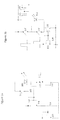
Figure 1a , for example, shows an example known pulsed mode laser diode driver circuit (from the perspective of one half of a steered current unary pair, in other words the other half of the differential pair is not shown for simplicity). Thelaser diode 100 is coupled with its anode to the positive supply and the cathode to the current driver circuit. In the example shown inFigure 1 a the circuit is provided with aclamp switch 113 in parallel with thelaser diode 100. The driver circuit shown inFigure 1 a shows a cascode arrangement with acascode transistor 103 coupled to the laser diode and which is coupled to acurrent switch 111 for current steering and which is coupled to acurrent sink transistor 107 which is then coupled to the negative supply rail. Thecascode transistor 103 is coupled by its gate to a mirroredcascode transistor 101, which is configured to mirror the current from the mirroredcascode transistor 101 to thecascode transistor 103 on a 1:N ratio. Thecurrent sink transistor 107 is also coupled by its gate to a mirroredcurrent sink transistor 105, which is configured to mirror the current from the mirroredcurrent sink transistor 105 to thecurrent sink transistor 107 on a 1:N ratio also. In this circuit by operating the current switch 111 a pulse of current defined by thecurrent sink transistor 107 can be provided to the laser diode. - Furthermore with respect to
Figure 1b a further known pulse mode laser diode driver circuit is shown. In this example circuit the cascode transistors shown inFigure 1 a are replaced with apre-bias transistor pair laser diode 120 is coupled with its anode to thepre-bias transistor pair current sink transistor 129 which is mirrored by the mirroredcurrent sink transistor 131. In the example shown inFigure 1b the circuit is provided with aclamp switch 127 in parallel with thelaser diode 120. The driver circuit shown inFigure 1b shows the pre-bias transistor pair arrangement with a firstpre-bias transistor 121 coupled to the laser diode and the positive supply rail and which is in parallel with acurrent switch 125. The firstpre-bias transistor 121 is coupled by its gate to a mirroredpre-bias transistor 131 which mirrors the current from on defined ratio. The circuit is configured to be operated by sequentially closing thecurrent switch 125 and then theclamp switch 127 to provide the laser diode with a pulse of current in order to produce the required output light intensity. - As well as being able to provide a current suitable for generating a current pulse a 'sine wave' current driver can be implemented.
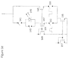
Figure 1c shows a unary branch of a known sine wave mode circuit. In the circuit shown inFigure 1c thelaser diode 140 is shown with an associatedclamp switch 143 in parallel with thelaser diode 140. Thelaser diode 140 further is coupled to the positive supply rail via anoperational switch 141 which is configured to be closed while the circuit is operational. The driver circuit shown inFigure 1c further shows an arrangement similar toFigure 1 a (but furthermore shows both switch paths for the unary DAC configuration) with acascode transistor 147 coupled to thelaser diode 140 and acurrent switch 153. The circuit further shows acurrent sink transistor 155 which is coupled to thecurrent switch 153 and the negative supply rail. - In parallel with the laser
operational switch 141, thelaser diode 140, thecascode transistor 147 and thecurrent switch 153 is afurther cascode transistor 145 and a furthercurrent switch 151 configured to provide the switch current path when the switch current path though the diode is not active. - The
cascode transistor 147 is common gate coupled to thefurther cascode transistor 145 and to a mirroredcascode transistor 149. The mirroredcascode transistor 149 is configured to mirror the current from the mirroredcascode transistor 149 to the cascode transistor 147 (and to the further cascode transistor 151) on a 1:N ratio. Thecurrent sink transistor 155 is also common gate coupled to a mirroredcurrent sink transistor 157 which mirrors the current from the mirroredcurrent sink transistor 157 to thecurrent sink transistor 155 on a 1:N ratio. An arbitrary wave may be generated by combining several of the driver circuits in parallel and by operating theswitches diode 140. - In such circuits the operation of the current steering switches 153 and 151 enable the switching on or off of the laser diode. However such circuits as shown in
Figures 1 a to 1 c have problems as have been raised earlier. - The circuits such as shown in
Figure 1 a and 1 c, by implementing a cascode arrangement in order to control Vdrain bias variation, have a switch rise and fall time which is defined by a parasitic gate capacitor Cg and the bias current Ibias of the current sink transistor. Furthermore the operating headroom of the cascode arrangement requires an operating voltage of Vov for both the cascode transistor. Vov, is the excess voltage of a MOSFET device (its Drain Source voltage) for which its mode of operation is in Saturation region. - The concept as implemented in embodiments shown herein is to provide a laser diode driver implementation which displaces the cascode transistors but enables matching to be performed using a suitable closed loop feedback circuit and which controls the current sink transistors via a suitable low impedance output.
-
Figure 2 shows an example implementation for a driver circuit which shows an embodiments of the laser diode driver concept.Figure 2 shows a modified version of the laser diode driver circuit shown inFigure 1c . In this circuit theoperational switch 203 is coupled to the parallel arrangement of thelaser diode 200 and clampswitch 201. Thelaser diode 200 may be coupled to acurrent sink transistor 209 which in turn is coupled to a firstcurrent steering switch 211 and which is in turn coupled to the negative supply rail. A current switch or shunt path shown by the arrow Is and which is arranged in parallel with theoperating switch 203,laser diode 200 andcurrent sink transistor 209 comprises a furthercurrent sink transistor 205 which is coupled to the positive supply rail and a secondcurrent steering switch 207, which is in turn coupled to the negative supply rail. - The
current sink transistor 209 and furthercurrent sink transistor 205 are gate coupled to afeedback transistor 213 which is configured to pass a feedback current If. Thefeedback transistor 213, thecurrent sink transistor 209 and the furthercurrent sink transistor 205 are furthermore driven or coupled to the low impedance output of anoperational amplifier 215. Theoperational amplifier 215 is configured to receive at a positive input a feedback voltage Vf and further configured to receive at the negative input a reference voltage Vr. - An advantage of a circuit such as shown in
Figure 2 is shown by a signal model at thecurrent sink transistor 209 and thecurrent steering switch 211 shown inFigure 3 . From the signal model it can be seen that the rise and fall times of the switching of the circuit are controlled by the gate capacitance Cg and the current which flows through the modelled ON resistance, Rds. Furthermore the Cg charge/discharge is performed via the resistor Rds and as such is defined by a dv/dt =Rds*Cg and not the current source such as shown inFigure 1c which causes a dv/dt = Ibias/Cg. Rds may be a MOSFET on small geometry process (e.g. 40nm). Such a MOSFET may present both reduction in switching gate capacitance and can be driven at native logic level (e.g. 1.1 V, hence the ease of using standard logic cells as pre-drivers), also doing away with the need for level shifting, which impedes frequency of switching. - An additional advantage of such a circuit is that the switching can be filtered via a separate supply voltage (coupled to the feedback current supply) which can reduce fluctuations on the positive supply rail for the laser diode.
- As also discussed the removal of the cascode transistor improves the operating headroom for the circuit. In order to enable or redeem this benefit the transistors should be operated in saturation modes.
- In order to generate a suitable regulation voltage for the laser diode the feedback loop attempts to simulate the operation of the laser diode for the current value driving the laser diode.
- In applications where the laser diode emits light of IR wavelength, a semiconductor material like Gallium Arsenide (GaAs) is commonly utilised. A model equivalent for GaAs for a forward biased voltage (Vf) may be approximated as two silicon (Si) diode drop. IR wavelengths are used because they are invisible to the human eye and thus may be implemented in applications such as communications where visibility is not desired perception. Although the approximation is described herein with respect to GaAs other semiconductor PN junctions may be approximated in some other embodiments (for example Homo-junction Si).
- Furthermore in order to simulate or model the current response of the laser diode it may be assumed that the laser diode (e.g. a VCSEL) is to be operated within the linear region of operation. This occurs when the diode is operated in the linear optical power output region above the pre-bias knee region at Ith, where it bounds the extinction of optical output power.
- As the optical power against current curve is intrinsic to the device structure may be modelled by the mesa resistance Rs which comprises the resistances from the P and N-Type distributed Bragg Reflector Mirrors, the sheet resistance from the n-contact layer and the P- and N- contacts and aperture of lasing window. In other words the feedback loop may model the current required for the laser diode to generate a light intensity value by using a resistor value Rs.
- Furthermore by modelling the values in the following manner it is possible to model the change of proportionality with respect to absolute temperature (Complementary, CTAT).
- An example of the generation of the reference and feedback voltage values which may be input to the
operational amplifier 215 are shown inFigure 4a. Figure 4a showscircuitry 400 comprising a modelled voltage forward basedvoltage generator 430 comprising a pair of forward biaseddiodes resistors diodes 430. FurthermoreFigure 4a shows the anode of thediode 407 which is driven by an output voltage from a digital-to-analogue (DAC)converter 420. TheDAC 420 can receive a digital input value which then outputs a suitable current output IDAC which impacts on the reference voltage input to the negative input of theoperational amplifier 215. - The feedback voltage generator part of the
circuitry 400 comprises a further modelled voltage forward based voltage generator comprising a further pair of forward biaseddiodes resistor 409 which is configured to simulate the voltage drop caused by the linear response of the laser diode (Rs). The 'golden'resistor 409 is then coupled to the drain of thefeedback transistor 213. In some embodiments the output of theoperational amplifier 215 is coupled to the negative supply rail by adecoupling capacitor 413. - In such a manner a scaled equivalent to the peak DC level of the lasing current can be generated or 'programmed' by using a current DAC. This circuit thus generates a set point voltage using the two forward biased Si diodes, for which the Operational Amplifier then generates the regulate voltage (VREG) and which is output and common gated to the elements such as shown in
Figure 2 and furthermore with then used by the feedback loop by a referencing or 'golden unit' element. The 'golden' unit, which inFigure 4a is shown as theresistor 409 generates a model drain-source current (IDS) and which is a ratio of the desired (or programmed) current (e.g. in this example a ratio of 1:1). - Furthermore in such embodiments the peak lasing current (or Full Scale, FS) is amplified by gains obtained by the open-loop current mirroring ratio of the golden unit to the summed unit elements that make up the unary DAC.
- In such embodiments it may be possible to overdrive VREG, as the MOSFET device goes from saturation to linear mode with an increasing of lasing current and thus in some embodiments enable an extension of operating supply range (the headroom limitation) with a set peak lasing current.
- The use of the feedback/tracking mechanism may in some embodiments be configured to be adjustable, for example by trimming the 'golden' resistor value for correction.
- A further example of a
circuit 450 for the generation of the reference and feedback voltage values which may be input to theoperational amplifier 215 are shown inFigure 4b . This example circuit is similar to the circuit shown infigure 4a and like reference numerals refer to like circuit components. The circuit additionally includes a pair ofresistors Resistor 415 is connected in series between the positive supply rail and thediodes Resistor 417 is connected between the positive supply rail and the regulator input.Resistor 417 may also be connected to the IDAC. - With respect to
Figure 5 the implementation examples shown inFigure 2 and4 are integrated into a top level schematic view of alaser diode circuit 600. - The laser diode circuit in this example comprises the
regulation voltage generator 400 which comprises a modelled voltage forward basedvoltage generator 430 comprising a pair of forward biaseddiodes diode 407 which is driven by an output voltage from a digital-to-analogue (DAC)converter 420, a further modelled voltage forward based voltage generator comprising a further pair of forward biaseddiodes resistor 409 which is configured to simulate the voltage drop caused by the linear response of the laser diode (Rs) and thetransistor 547 in parallel with the resistor which may simulate the non-linear voltage drop of the laser diode when not in the linear response region. The 'golden'element resistor 409 is then coupled to the drain of thefeedback transistor 213. The circuit is shown further comprising afurther transistor 534 coupled between the source of thefeedback transistor 213 and the negative supply rail which simulates the effect of the current steering switches. - The current driver is further shown with the current steering switches 211 and 213 as shown in
Figure 2 implemented astransistors decoder 535 which receives the digital to analogue converter input and switches between the diode and shunt current switch paths. - Furthermore the circuit is shown with a pre-bias module which comprises
transistors - The
clamp switch 201 is shown implemented as a switch input which is coupled to the gate of annmos transistor 511 and to the input of aninverter 513, the output of which is further coupled to the gate of apmos transistor 515, where the nmos and pmos transistors are coupled in parallel with thelaser diode 200. - The
operational switch 203 is shown implemented as atransistor 507 coupled between the positive supply rail and thelaser diode 200. - A current monitor in the form of a voltage to
current converter 509 is shown coupled to the laser diode and furthermore a current measurement may be provided by atransistor 541 gate coupled to the output of the operational amplifier and further enabled by ameasurement selector transistor 537. - Furthermore the circuit is shown with a clock/pulse snubber comprising
complimentary transistors capacitor 505. This is another patent disclosure that's placed on hold, its benefit is yet to be evaluated on silicon, it decreases the fall time Tf of the pulse negative edge. - Various embodiments with different variations have been described here above. It should be noted that those skilled in the art may combine various elements of these various embodiments and variations.
- Such alterations, modifications, and improvements are intended to be part of this disclosure, and are intended to be within the scope of the present invention. Accordingly, the foregoing description is by way of example only and is not intended to be limiting. The present invention is limited only as defined in the following claims and the equivalents thereto.
Claims (15)
- A driver circuit for a laser diode configured to pass a current, said circuit comprising:a first transistor connected in series with the laser diode, and configured to regulate the current; anda voltage regulator configured to provide an input to a gate of the first transistor so as to regulate the current in dependence upon a regulator input and a feedback input at the voltage regulator.
- A driver circuit as claimed in claim 1, wherein the voltage regulator comprises an operational amplifier.
- A driver circuit as claimed in claim 2, wherein the regulator input of the operational amplifier is an inverting input, and the feedback input of the operational amplifier is a non-inverting input.
- A driver circuit as claimed in any preceding claim, further comprising:a digital to analogue converter configured to output an analogue signal to the regulator input of the voltage regulator, wherein the analogue signal is based on a digital representation of a laser diode output level.
- A driver circuit as claimed in any preceding claim, wherein the digital representation of a laser diode output level comprises a digital representation of:a continuous wave laser output; anda pulsed mode laser output.
- A driver circuit as claimed in any preceding claim, further comprising:a shunt path arranged in parallel to the laser diode, the shunt path comprising a second transistor configured to regulate a current in the shunt path in dependence upon an input provided by the voltage regulator; andone or more switches configured to switch a flow of current between the laser diode and the shunt path.
- A driver circuit as claimed in any preceding claim, further comprising:a resistor connected to the feedback input of the voltage regulator, wherein the resistor is configured to simulate a voltage drop resulting from a linear response of the laser diode.
- A driver circuit as claimed in any preceding claim, further comprising a modelled voltage forward based voltage generator configured to provide an input to the regulator input.
- A driver circuit as claimed in claim 8, wherein the modelled voltage forward based voltage generator comprises one or more forward biased diodes.
- A driver circuit as claimed in claims 8 or 9, wherein the modelled voltage forward based voltage generator comprises one or more resistors.
- A driver circuit as claimed in any preceding claim, further comprising:a clamp switch connected in parallel with the laser diode.
- A driver circuit as claimed in any preceding claim, wherein the laser diode is configured to be operated within a linear region of operation.
- A driver circuit as claimed in any preceding claim, wherein the laser diode is a vertical cavity surface emitting laser diode.
- A driver circuit as claimed in any preceding claim, further comprising:a positive supply rail connected to the anode of the laser diode; anda negative supply rail connected to the cathode of the laser diode,wherein the positive supply rail and negative supply terminal are configured to provide the current.
- A method for operating a driving circuit for a laser diode configured to pass a current, said method comprising:regulating the current by a first transistor connected in series with the laser diode; andproviding an input to a gate of the first transistor by a voltage regulator so as to regulate the current in dependence upon a regulator input and a feedback input at the voltage regulator.
Priority Applications (2)
| Application Number | Priority Date | Filing Date | Title |
|---|---|---|---|
| EP16189306.0A EP3297105B1 (en) | 2016-09-16 | 2016-09-16 | Driver circuit for a laser diode |
| US15/476,108 US10074961B2 (en) | 2016-09-16 | 2017-03-31 | Laser driver circuit and method of operating thereof |
Applications Claiming Priority (1)
| Application Number | Priority Date | Filing Date | Title |
|---|---|---|---|
| EP16189306.0A EP3297105B1 (en) | 2016-09-16 | 2016-09-16 | Driver circuit for a laser diode |
Publications (2)
| Publication Number | Publication Date |
|---|---|
| EP3297105A1 true EP3297105A1 (en) | 2018-03-21 |
| EP3297105B1 EP3297105B1 (en) | 2021-05-12 |
Family
ID=56979382
Family Applications (1)
| Application Number | Title | Priority Date | Filing Date |
|---|---|---|---|
| EP16189306.0A Active EP3297105B1 (en) | 2016-09-16 | 2016-09-16 | Driver circuit for a laser diode |
Country Status (2)
| Country | Link |
|---|---|
| US (1) | US10074961B2 (en) |
| EP (1) | EP3297105B1 (en) |
Cited By (3)
| Publication number | Priority date | Publication date | Assignee | Title |
|---|---|---|---|---|
| WO2021213665A1 (en) * | 2020-04-24 | 2021-10-28 | Huawei Technologies Co., Ltd. | Laser driver |
| US11996675B2 (en) | 2018-07-10 | 2024-05-28 | Sony Semiconductor Solutions Corporation | Laser drive circuit and sensor apparatus |
| US20240305377A1 (en) * | 2021-12-07 | 2024-09-12 | Prose Technologies (Suzhou) Co., Ltd. | Optical module |
Families Citing this family (6)
| Publication number | Priority date | Publication date | Assignee | Title |
|---|---|---|---|---|
| JP7063651B2 (en) * | 2018-02-19 | 2022-05-09 | エイブリック株式会社 | Signal detection circuit and signal detection method |
| EP3588703A1 (en) | 2018-06-21 | 2020-01-01 | STMicroelectronics (Research & Development) Limited | Laser diode current driving apparatus |
| CN111065187B (en) * | 2018-10-17 | 2022-04-26 | 戴洛格半导体(英国)有限公司 | Current regulator |
| JP2020088020A (en) * | 2018-11-16 | 2020-06-04 | ソニーセミコンダクタソリューションズ株式会社 | Detection circuit, drive circuit, and light-emitting device |
| FR3119250A1 (en) * | 2021-01-22 | 2022-07-29 | Stmicroelectronics (Grenoble 2) Sas | LOW SIDE DRIVER FOR LASER DIODE |
| US20230318711A1 (en) * | 2022-04-05 | 2023-10-05 | Fathom Radiant, PBC | Optical Transceiver Methods and Apparatus for Integrated Optical Links |
Citations (4)
| Publication number | Priority date | Publication date | Assignee | Title |
|---|---|---|---|---|
| US5123023A (en) * | 1990-11-21 | 1992-06-16 | Polaroid Corporation | Laser driver with plural feedback loops |
| US6026104A (en) * | 1997-04-24 | 2000-02-15 | Oki Electric Industry Co., Ltd. | Apparatus for controlling laser diode |
| US6711189B1 (en) * | 2000-02-04 | 2004-03-23 | Stratos Lightwave, Inc. | Automatic power control and laser slope efficiency normalizing circuit |
| US20060072867A1 (en) * | 2004-09-28 | 2006-04-06 | Toru Kawagishi | Optical transmitter |
Family Cites Families (8)
| Publication number | Priority date | Publication date | Assignee | Title |
|---|---|---|---|---|
| US5936986A (en) | 1996-07-30 | 1999-08-10 | Bayer Corporation | Methods and apparatus for driving a laser diode |
| JP4408010B2 (en) * | 1999-07-01 | 2010-02-03 | 富士通株式会社 | Optical transmitter for WDM |
| JP4557481B2 (en) * | 1999-08-03 | 2010-10-06 | 富士通株式会社 | Semiconductor laser driving circuit and driving method |
| US6917639B2 (en) | 2001-08-09 | 2005-07-12 | Ricoh Company, Ltd. | Laser driver circuit |
| US7792166B2 (en) | 2005-06-24 | 2010-09-07 | Lockheed Martin Corporation | Apparatus and method for driving laser diodes |
| JP5092318B2 (en) * | 2006-08-30 | 2012-12-05 | 日本電気株式会社 | Optical transmitter, its operation control method and program |
| US8401388B2 (en) | 2009-06-22 | 2013-03-19 | Stmicroelectronics S.R.L. | Optical transmitter |
| JP6494532B2 (en) * | 2013-02-28 | 2019-04-03 | ローレンス リバモア ナショナル セキュリティー, エルエルシー | Compact high current high efficiency laser diode driver |
-
2016
- 2016-09-16 EP EP16189306.0A patent/EP3297105B1/en active Active
-
2017
- 2017-03-31 US US15/476,108 patent/US10074961B2/en active Active
Patent Citations (4)
| Publication number | Priority date | Publication date | Assignee | Title |
|---|---|---|---|---|
| US5123023A (en) * | 1990-11-21 | 1992-06-16 | Polaroid Corporation | Laser driver with plural feedback loops |
| US6026104A (en) * | 1997-04-24 | 2000-02-15 | Oki Electric Industry Co., Ltd. | Apparatus for controlling laser diode |
| US6711189B1 (en) * | 2000-02-04 | 2004-03-23 | Stratos Lightwave, Inc. | Automatic power control and laser slope efficiency normalizing circuit |
| US20060072867A1 (en) * | 2004-09-28 | 2006-04-06 | Toru Kawagishi | Optical transmitter |
Cited By (3)
| Publication number | Priority date | Publication date | Assignee | Title |
|---|---|---|---|---|
| US11996675B2 (en) | 2018-07-10 | 2024-05-28 | Sony Semiconductor Solutions Corporation | Laser drive circuit and sensor apparatus |
| WO2021213665A1 (en) * | 2020-04-24 | 2021-10-28 | Huawei Technologies Co., Ltd. | Laser driver |
| US20240305377A1 (en) * | 2021-12-07 | 2024-09-12 | Prose Technologies (Suzhou) Co., Ltd. | Optical module |
Also Published As
| Publication number | Publication date |
|---|---|
| EP3297105B1 (en) | 2021-05-12 |
| US20180083419A1 (en) | 2018-03-22 |
| US10074961B2 (en) | 2018-09-11 |
Similar Documents
| Publication | Publication Date | Title |
|---|---|---|
| US10074961B2 (en) | Laser driver circuit and method of operating thereof | |
| CN107850910B (en) | Wide-voltage range low dropout regulator | |
| EP0525819A1 (en) | A pulse amplifier suitable for use in a semiconductor laser driving device | |
| CN108711735B (en) | Temperature compensation circuit for direct-modulated laser drivers | |
| JP6576306B2 (en) | Voltage-current conversion circuit and load drive circuit | |
| CN104682190A (en) | Laser diode driver | |
| JP6097713B2 (en) | Light emitting element driving circuit, light source device, and light emitting element driving method | |
| JP4566692B2 (en) | LIGHT EMITTING DIODE DRIVING DEVICE AND OPTICAL TRANSMISSION DEVICE HAVING THE SAME | |
| US8125273B2 (en) | Apparatus and method for driving an LED | |
| JP2004328640A (en) | Bias current generating circuit, laser diode driving circuit, and transmitter for optical communication | |
| US7068691B2 (en) | Directly modulated optical module and method for driving semiconductor laser included therein | |
| CN114185052B (en) | Laser emission driving circuit and laser radar | |
| KR20230166898A (en) | Current-controlled segmented laser driver | |
| JP7283063B2 (en) | amplifier circuit | |
| US7952342B2 (en) | Constant current source apparatus | |
| JP7338985B2 (en) | drive circuit | |
| US7141936B2 (en) | Driving circuit for light emitting diode | |
| CN110120627B (en) | Light-emitting element driver circuit | |
| US7280574B1 (en) | Circuit for driving a laser diode and method | |
| US9641170B2 (en) | Pass device with boost voltage regulation and current gain for VCSEL driving applications | |
| JP6922505B2 (en) | Semiconductor laser drive circuit | |
| KR102128850B1 (en) | Smart fet circuit | |
| JP4790306B2 (en) | Laser diode drive circuit | |
| US12483201B1 (en) | Parametric-insensitive edge rate control in switched-power circuits with tailored power supply voltage sensitivity | |
| KR100448734B1 (en) | Low voltage Current driving circuit |
Legal Events
| Date | Code | Title | Description |
|---|---|---|---|
| PUAI | Public reference made under article 153(3) epc to a published international application that has entered the european phase |
Free format text: ORIGINAL CODE: 0009012 |
|
| STAA | Information on the status of an ep patent application or granted ep patent |
Free format text: STATUS: THE APPLICATION HAS BEEN PUBLISHED |
|
| AK | Designated contracting states |
Kind code of ref document: A1 Designated state(s): AL AT BE BG CH CY CZ DE DK EE ES FI FR GB GR HR HU IE IS IT LI LT LU LV MC MK MT NL NO PL PT RO RS SE SI SK SM TR |
|
| AX | Request for extension of the european patent |
Extension state: BA ME |
|
| STAA | Information on the status of an ep patent application or granted ep patent |
Free format text: STATUS: REQUEST FOR EXAMINATION WAS MADE |
|
| 17P | Request for examination filed |
Effective date: 20180328 |
|
| RBV | Designated contracting states (corrected) |
Designated state(s): AL AT BE BG CH CY CZ DE DK EE ES FI FR GB GR HR HU IE IS IT LI LT LU LV MC MK MT NL NO PL PT RO RS SE SI SK SM TR |
|
| STAA | Information on the status of an ep patent application or granted ep patent |
Free format text: STATUS: EXAMINATION IS IN PROGRESS |
|
| 17Q | First examination report despatched |
Effective date: 20190909 |
|
| GRAP | Despatch of communication of intention to grant a patent |
Free format text: ORIGINAL CODE: EPIDOSNIGR1 |
|
| STAA | Information on the status of an ep patent application or granted ep patent |
Free format text: STATUS: GRANT OF PATENT IS INTENDED |
|
| RIC1 | Information provided on ipc code assigned before grant |
Ipc: H01S 5/062 20060101ALI20201103BHEP Ipc: H01S 5/042 20060101AFI20201103BHEP Ipc: H05B 33/08 20200101ALI20201103BHEP Ipc: H05B 45/48 20200101ALI20201103BHEP Ipc: H01S 5/0683 20060101ALN20201103BHEP |
|
| INTG | Intention to grant announced |
Effective date: 20201127 |
|
| RIC1 | Information provided on ipc code assigned before grant |
Ipc: H01S 5/042 20060101AFI20201117BHEP Ipc: H05B 33/08 20200101ALI20201117BHEP Ipc: H01S 5/062 20060101ALI20201117BHEP Ipc: H05B 45/48 20200101ALI20201117BHEP Ipc: H01S 5/0683 20060101ALN20201117BHEP |
|
| GRAS | Grant fee paid |
Free format text: ORIGINAL CODE: EPIDOSNIGR3 |
|
| GRAA | (expected) grant |
Free format text: ORIGINAL CODE: 0009210 |
|
| STAA | Information on the status of an ep patent application or granted ep patent |
Free format text: STATUS: THE PATENT HAS BEEN GRANTED |
|
| AK | Designated contracting states |
Kind code of ref document: B1 Designated state(s): AL AT BE BG CH CY CZ DE DK EE ES FI FR GB GR HR HU IE IS IT LI LT LU LV MC MK MT NL NO PL PT RO RS SE SI SK SM TR |
|
| REG | Reference to a national code |
Ref country code: GB Ref legal event code: FG4D |
|
| REG | Reference to a national code |
Ref country code: CH Ref legal event code: EP |
|
| REG | Reference to a national code |
Ref country code: DE Ref legal event code: R096 Ref document number: 602016057693 Country of ref document: DE |
|
| REG | Reference to a national code |
Ref country code: IE Ref legal event code: FG4D |
|
| REG | Reference to a national code |
Ref country code: AT Ref legal event code: REF Ref document number: 1392811 Country of ref document: AT Kind code of ref document: T Effective date: 20210615 |
|
| REG | Reference to a national code |
Ref country code: LT Ref legal event code: MG9D |
|
| REG | Reference to a national code |
Ref country code: AT Ref legal event code: MK05 Ref document number: 1392811 Country of ref document: AT Kind code of ref document: T Effective date: 20210512 |
|
| REG | Reference to a national code |
Ref country code: NL Ref legal event code: MP Effective date: 20210512 |
|
| PG25 | Lapsed in a contracting state [announced via postgrant information from national office to epo] |
Ref country code: FI Free format text: LAPSE BECAUSE OF FAILURE TO SUBMIT A TRANSLATION OF THE DESCRIPTION OR TO PAY THE FEE WITHIN THE PRESCRIBED TIME-LIMIT Effective date: 20210512 Ref country code: LT Free format text: LAPSE BECAUSE OF FAILURE TO SUBMIT A TRANSLATION OF THE DESCRIPTION OR TO PAY THE FEE WITHIN THE PRESCRIBED TIME-LIMIT Effective date: 20210512 Ref country code: HR Free format text: LAPSE BECAUSE OF FAILURE TO SUBMIT A TRANSLATION OF THE DESCRIPTION OR TO PAY THE FEE WITHIN THE PRESCRIBED TIME-LIMIT Effective date: 20210512 Ref country code: AT Free format text: LAPSE BECAUSE OF FAILURE TO SUBMIT A TRANSLATION OF THE DESCRIPTION OR TO PAY THE FEE WITHIN THE PRESCRIBED TIME-LIMIT Effective date: 20210512 Ref country code: BG Free format text: LAPSE BECAUSE OF FAILURE TO SUBMIT A TRANSLATION OF THE DESCRIPTION OR TO PAY THE FEE WITHIN THE PRESCRIBED TIME-LIMIT Effective date: 20210812 |
|
| PG25 | Lapsed in a contracting state [announced via postgrant information from national office to epo] |
Ref country code: GR Free format text: LAPSE BECAUSE OF FAILURE TO SUBMIT A TRANSLATION OF THE DESCRIPTION OR TO PAY THE FEE WITHIN THE PRESCRIBED TIME-LIMIT Effective date: 20210813 Ref country code: LV Free format text: LAPSE BECAUSE OF FAILURE TO SUBMIT A TRANSLATION OF THE DESCRIPTION OR TO PAY THE FEE WITHIN THE PRESCRIBED TIME-LIMIT Effective date: 20210512 Ref country code: IS Free format text: LAPSE BECAUSE OF FAILURE TO SUBMIT A TRANSLATION OF THE DESCRIPTION OR TO PAY THE FEE WITHIN THE PRESCRIBED TIME-LIMIT Effective date: 20210912 Ref country code: PL Free format text: LAPSE BECAUSE OF FAILURE TO SUBMIT A TRANSLATION OF THE DESCRIPTION OR TO PAY THE FEE WITHIN THE PRESCRIBED TIME-LIMIT Effective date: 20210512 Ref country code: NO Free format text: LAPSE BECAUSE OF FAILURE TO SUBMIT A TRANSLATION OF THE DESCRIPTION OR TO PAY THE FEE WITHIN THE PRESCRIBED TIME-LIMIT Effective date: 20210812 Ref country code: PT Free format text: LAPSE BECAUSE OF FAILURE TO SUBMIT A TRANSLATION OF THE DESCRIPTION OR TO PAY THE FEE WITHIN THE PRESCRIBED TIME-LIMIT Effective date: 20210913 Ref country code: SE Free format text: LAPSE BECAUSE OF FAILURE TO SUBMIT A TRANSLATION OF THE DESCRIPTION OR TO PAY THE FEE WITHIN THE PRESCRIBED TIME-LIMIT Effective date: 20210512 Ref country code: RS Free format text: LAPSE BECAUSE OF FAILURE TO SUBMIT A TRANSLATION OF THE DESCRIPTION OR TO PAY THE FEE WITHIN THE PRESCRIBED TIME-LIMIT Effective date: 20210512 |
|
| PG25 | Lapsed in a contracting state [announced via postgrant information from national office to epo] |
Ref country code: NL Free format text: LAPSE BECAUSE OF FAILURE TO SUBMIT A TRANSLATION OF THE DESCRIPTION OR TO PAY THE FEE WITHIN THE PRESCRIBED TIME-LIMIT Effective date: 20210512 |
|
| PG25 | Lapsed in a contracting state [announced via postgrant information from national office to epo] |
Ref country code: SM Free format text: LAPSE BECAUSE OF FAILURE TO SUBMIT A TRANSLATION OF THE DESCRIPTION OR TO PAY THE FEE WITHIN THE PRESCRIBED TIME-LIMIT Effective date: 20210512 Ref country code: SK Free format text: LAPSE BECAUSE OF FAILURE TO SUBMIT A TRANSLATION OF THE DESCRIPTION OR TO PAY THE FEE WITHIN THE PRESCRIBED TIME-LIMIT Effective date: 20210512 Ref country code: DK Free format text: LAPSE BECAUSE OF FAILURE TO SUBMIT A TRANSLATION OF THE DESCRIPTION OR TO PAY THE FEE WITHIN THE PRESCRIBED TIME-LIMIT Effective date: 20210512 Ref country code: EE Free format text: LAPSE BECAUSE OF FAILURE TO SUBMIT A TRANSLATION OF THE DESCRIPTION OR TO PAY THE FEE WITHIN THE PRESCRIBED TIME-LIMIT Effective date: 20210512 Ref country code: CZ Free format text: LAPSE BECAUSE OF FAILURE TO SUBMIT A TRANSLATION OF THE DESCRIPTION OR TO PAY THE FEE WITHIN THE PRESCRIBED TIME-LIMIT Effective date: 20210512 Ref country code: RO Free format text: LAPSE BECAUSE OF FAILURE TO SUBMIT A TRANSLATION OF THE DESCRIPTION OR TO PAY THE FEE WITHIN THE PRESCRIBED TIME-LIMIT Effective date: 20210512 Ref country code: ES Free format text: LAPSE BECAUSE OF FAILURE TO SUBMIT A TRANSLATION OF THE DESCRIPTION OR TO PAY THE FEE WITHIN THE PRESCRIBED TIME-LIMIT Effective date: 20210512 |
|
| REG | Reference to a national code |
Ref country code: DE Ref legal event code: R097 Ref document number: 602016057693 Country of ref document: DE |
|
| PLBE | No opposition filed within time limit |
Free format text: ORIGINAL CODE: 0009261 |
|
| STAA | Information on the status of an ep patent application or granted ep patent |
Free format text: STATUS: NO OPPOSITION FILED WITHIN TIME LIMIT |
|
| 26N | No opposition filed |
Effective date: 20220215 |
|
| REG | Reference to a national code |
Ref country code: CH Ref legal event code: PL |
|
| REG | Reference to a national code |
Ref country code: BE Ref legal event code: MM Effective date: 20210930 |
|
| GBPC | Gb: european patent ceased through non-payment of renewal fee |
Effective date: 20210916 |
|
| PG25 | Lapsed in a contracting state [announced via postgrant information from national office to epo] |
Ref country code: IS Free format text: LAPSE BECAUSE OF FAILURE TO SUBMIT A TRANSLATION OF THE DESCRIPTION OR TO PAY THE FEE WITHIN THE PRESCRIBED TIME-LIMIT Effective date: 20210912 Ref country code: MC Free format text: LAPSE BECAUSE OF FAILURE TO SUBMIT A TRANSLATION OF THE DESCRIPTION OR TO PAY THE FEE WITHIN THE PRESCRIBED TIME-LIMIT Effective date: 20210512 Ref country code: AL Free format text: LAPSE BECAUSE OF FAILURE TO SUBMIT A TRANSLATION OF THE DESCRIPTION OR TO PAY THE FEE WITHIN THE PRESCRIBED TIME-LIMIT Effective date: 20210512 |
|
| PG25 | Lapsed in a contracting state [announced via postgrant information from national office to epo] |
Ref country code: LU Free format text: LAPSE BECAUSE OF NON-PAYMENT OF DUE FEES Effective date: 20210916 Ref country code: IT Free format text: LAPSE BECAUSE OF FAILURE TO SUBMIT A TRANSLATION OF THE DESCRIPTION OR TO PAY THE FEE WITHIN THE PRESCRIBED TIME-LIMIT Effective date: 20210512 Ref country code: IE Free format text: LAPSE BECAUSE OF NON-PAYMENT OF DUE FEES Effective date: 20210916 Ref country code: GB Free format text: LAPSE BECAUSE OF NON-PAYMENT OF DUE FEES Effective date: 20210916 Ref country code: FR Free format text: LAPSE BECAUSE OF NON-PAYMENT OF DUE FEES Effective date: 20210930 Ref country code: BE Free format text: LAPSE BECAUSE OF NON-PAYMENT OF DUE FEES Effective date: 20210930 |
|
| PG25 | Lapsed in a contracting state [announced via postgrant information from national office to epo] |
Ref country code: LI Free format text: LAPSE BECAUSE OF NON-PAYMENT OF DUE FEES Effective date: 20210930 Ref country code: CH Free format text: LAPSE BECAUSE OF NON-PAYMENT OF DUE FEES Effective date: 20210930 |
|
| PG25 | Lapsed in a contracting state [announced via postgrant information from national office to epo] |
Ref country code: HU Free format text: LAPSE BECAUSE OF FAILURE TO SUBMIT A TRANSLATION OF THE DESCRIPTION OR TO PAY THE FEE WITHIN THE PRESCRIBED TIME-LIMIT; INVALID AB INITIO Effective date: 20160916 |
|
| PG25 | Lapsed in a contracting state [announced via postgrant information from national office to epo] |
Ref country code: CY Free format text: LAPSE BECAUSE OF FAILURE TO SUBMIT A TRANSLATION OF THE DESCRIPTION OR TO PAY THE FEE WITHIN THE PRESCRIBED TIME-LIMIT Effective date: 20210512 |
|
| PG25 | Lapsed in a contracting state [announced via postgrant information from national office to epo] |
Ref country code: MK Free format text: LAPSE BECAUSE OF FAILURE TO SUBMIT A TRANSLATION OF THE DESCRIPTION OR TO PAY THE FEE WITHIN THE PRESCRIBED TIME-LIMIT Effective date: 20210512 |
|
| PG25 | Lapsed in a contracting state [announced via postgrant information from national office to epo] |
Ref country code: MT Free format text: LAPSE BECAUSE OF FAILURE TO SUBMIT A TRANSLATION OF THE DESCRIPTION OR TO PAY THE FEE WITHIN THE PRESCRIBED TIME-LIMIT Effective date: 20210512 |
|
| PGFP | Annual fee paid to national office [announced via postgrant information from national office to epo] |
Ref country code: DE Payment date: 20250820 Year of fee payment: 10 |
|
| PG25 | Lapsed in a contracting state [announced via postgrant information from national office to epo] |
Ref country code: TR Free format text: LAPSE BECAUSE OF FAILURE TO SUBMIT A TRANSLATION OF THE DESCRIPTION OR TO PAY THE FEE WITHIN THE PRESCRIBED TIME-LIMIT Effective date: 20210512 |
|
| REG | Reference to a national code |
Ref country code: DE Ref legal event code: R082 Ref document number: 602016057693 Country of ref document: DE Representative=s name: WESTPHAL, MUSSGNUG & PARTNER PATENTANWAELTE MI, DE |