EP3297006A1 - Integration of inductor and damper for power filters - Google Patents
Integration of inductor and damper for power filters Download PDFInfo
- Publication number
- EP3297006A1 EP3297006A1 EP17178310.3A EP17178310A EP3297006A1 EP 3297006 A1 EP3297006 A1 EP 3297006A1 EP 17178310 A EP17178310 A EP 17178310A EP 3297006 A1 EP3297006 A1 EP 3297006A1
- Authority
- EP
- European Patent Office
- Prior art keywords
- inductor
- resistive element
- resistor
- substrate
- pair
- Prior art date
- Legal status (The legal status is an assumption and is not a legal conclusion. Google has not performed a legal analysis and makes no representation as to the accuracy of the status listed.)
- Granted
Links
Images




Classifications
-
- H—ELECTRICITY
- H01—ELECTRIC ELEMENTS
- H01F—MAGNETS; INDUCTANCES; TRANSFORMERS; SELECTION OF MATERIALS FOR THEIR MAGNETIC PROPERTIES
- H01F27/00—Details of transformers or inductances, in general
- H01F27/40—Structural association with built-in electric component, e.g. fuse
-
- H—ELECTRICITY
- H01—ELECTRIC ELEMENTS
- H01C—RESISTORS
- H01C3/00—Non-adjustable metal resistors made of wire or ribbon, e.g. coiled, woven or formed as grids
- H01C3/06—Flexible or folding resistors, whereby such a resistor can be looped or collapsed upon itself
-
- H—ELECTRICITY
- H01—ELECTRIC ELEMENTS
- H01F—MAGNETS; INDUCTANCES; TRANSFORMERS; SELECTION OF MATERIALS FOR THEIR MAGNETIC PROPERTIES
- H01F17/00—Fixed inductances of the signal type
- H01F17/04—Fixed inductances of the signal type with magnetic core
- H01F17/06—Fixed inductances of the signal type with magnetic core with core substantially closed in itself, e.g. toroid
- H01F17/062—Toroidal core with turns of coil around it
-
- H—ELECTRICITY
- H03—ELECTRONIC CIRCUITRY
- H03H—IMPEDANCE NETWORKS, e.g. RESONANT CIRCUITS; RESONATORS
- H03H7/00—Multiple-port networks comprising only passive electrical elements as network components
- H03H7/01—Frequency selective two-port networks
- H03H7/06—Frequency selective two-port networks including resistors
-
- H—ELECTRICITY
- H02—GENERATION; CONVERSION OR DISTRIBUTION OF ELECTRIC POWER
- H02M—APPARATUS FOR CONVERSION BETWEEN AC AND AC, BETWEEN AC AND DC, OR BETWEEN DC AND DC, AND FOR USE WITH MAINS OR SIMILAR POWER SUPPLY SYSTEMS; CONVERSION OF DC OR AC INPUT POWER INTO SURGE OUTPUT POWER; CONTROL OR REGULATION THEREOF
- H02M1/00—Details of apparatus for conversion
- H02M1/12—Arrangements for reducing harmonics from AC input or output
- H02M1/126—Arrangements for reducing harmonics from AC input or output using passive filters
Definitions
- the present disclosure relates to power filter circuits, and more specifically, to integration of an inductor and damper for a power filter circuit.
- a resistor (R) in series with an inductor L d also forms a damper circuit.
- the resistor is configured across the filter inductor L, and in FIG. 4 it is across filter capacitor (C).
- component C d or L d may be eliminated to have topologies shown in FIG. 5 and/or FIG. 6 .
- FIG. 10 depicts a resistive pattern on 1002 (shown in greater detail with respect to FIGS. 11 and 12 ) on a substrate 1008.
- a resistive pattern 1002 may be printed on a substrate 1008 and inserted between a toroidal inductor 1004 (around an outer periphery of inductor 1004) between the inductor 1004 and a toroidal inductor housing 1006.
- Substrate 1008 may be any circuit-printable substrate used for printing resistive circuits.
- Substrate 1008 may be flexible such that it is manipulatable around a periphery of an object, such as toroidal inductor housing 1006.
Landscapes
- Engineering & Computer Science (AREA)
- Power Engineering (AREA)
- Microelectronics & Electronic Packaging (AREA)
- Coils Or Transformers For Communication (AREA)
- Filters And Equalizers (AREA)
Abstract
Description
- The present disclosure relates to power filter circuits, and more specifically, to integration of an inductor and damper for a power filter circuit.
- A basic building block of a power filter is a low pass filter including an inductor (L) and a capacitor (C). This filter can also contain a damper circuit including a capacitor and a damper resistor (R). Prior art damper resistors use off-the-shelf resistors that may be either thick film or metal foil resistors. Resistor failures have been the leading cause for failures of various motor controllers during production process. The prime causes of the resistor failures are due to fragile ceramic base and low pulse power capability of the resistor element.
- Conventional wire wound resistors are generally large and bulky. The package style would require wire harness and supports that increase the production time and cost significantly, and also reduce overall reliability. It may be advantageous to integrate the resistor into the filter inductor package without changing its size. By integrating the resistor into inductor package the printed wiring assembly, component count and factory assembly time can be reduced, and the pulse power capability can also be increased by several order of magnitude hence improved reliability.
- According to an embodiment of the present invention, an inductor damper circuit includes a toroidal inductor having an inductor coil and an inductor housing, and a resistive element configured around a periphery of the inductor coil and having one end connected to the toroidal inductor. The resistive element is printed on a flexible substrate and configured to the inductor coil. The resistive element is integrated within the inductor housing with the toroidal inductor.
- According to other embodiments, an inductor damper circuit includes a toroidal inductor having an inductor coil and an inductor housing; and a resistive element on a flexible insulating disk at a base of the inductor coil and having one end connected to the toroidal inductor. The resistive element is printed on a flexible substrate and configured between the inductor coil and the inductor housing. The resistive element is integrated within the inductor housing with the toroidal inductor.
- The subject matter which is regarded as the invention is particularly pointed out and distinctly claimed in the claims at the conclusion of the specification. The forgoing and other features, and advantages of the invention are apparent from the following detailed description taken in conjunction with the accompanying drawings in which:
-
FIG. 1 depicts a filter circuit having an indicative damper connected across a filter inductor according to an embodiment; -
FIG. 2 depicts a filter circuit having a capacitive damper connected across a filter capacitor according to an embodiment; -
FIG. 3 depicts another filter circuit having an inductive damper connected across the filter inductor according to an embodiment; -
FIG. 4 depicts a circuit having an inductive damper connected across the filter capacitor according to an embodiment; -
FIG. 5 depicts a simplified filter circuit having a damper resistor connected across a filter inductor according to an embodiment; -
FIG. 6 depicts another simplified filter circuit having a damper resistor connected across a filter capacitor according to an embodiment; -
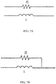
FIG. 7A depicts a terminal arrangement according to an embodiment; -
FIG. 7B depicts another conventional terminal arrangement according to an embodiment; -
FIG. 8 depicts an exemplary resistive pattern printed on a flex disk according to an embodiment; -
FIG. 9 depicts an exemplary resistive pattern printed on a flex disk and inserted between a toroidal inductor and a toroidal inductor housing, according to one embodiment; -
FIG. 10 depicts a resistive pattern printed on a strip-type resistor and inserted between a toroidal inductor and a toroidal inductor housing according to one embodiment; -
FIG. 11 depicts a resistive element pattern for a strip-type resistor according to one embodiment; -
FIG. 12 depicts a resistive element pattern for a strip-type resistor according to one embodiment; -
FIG. 13 depicts a resistive element pattern for a strip-type resistor according to one embodiment; and -
FIG. 14 depicts a resistive element pattern for a strip-type resistor according to one embodiment. - Common electromagnetic interference (EMI) filters and harmonic filters topologies are shown in
FIG. 1 through FIG. 4 . They differ from each other in the type of damper circuits and locations of the damper circuits. For example resistor (R) in series with a capacitor (Cd) forms a damper circuit. In topology shown inFIG. 1 , a damper circuit may be connected across the filter inductor (L), while inFIG. 2 it can be connected across the filter capacitor (C). - Similarly, a resistor (R) in series with an inductor Ld also forms a damper circuit. In
FIG. 3 , the resistor is configured across the filter inductor L, and inFIG. 4 it is across filter capacitor (C). According to some embodiments, and depending on application requirements, component Cd or Ld may be eliminated to have topologies shown inFIG. 5 and/orFIG. 6 . - In all embodiments depicted herein, one end of the damper resistor may be connected to a terminal of the inductor. Therefore the combined damper resistor and inductor may have all four terminals brought out or have three terminals brought out, as depicted in
FIGS. 7A and 7B . - In one embodiment, the resistive pattern is printed on a flexible strip base substrate material and then wrapped around the toroid (as shown in
FIG. 10 ), while in other embodiments, the resistive pattern is printed on a disk shaped flexible base material and inserted between the toroidal inductor and its housing (as shown inFIG. 9 ). The printed resistive pattern could be as shown inFIG. 11 or FIG. 12 for flexible strip and asFIG. 13 and FIG. 14 for a flexible disk. - Now, considering the figures in more detail,
FIGS. 1 and 2 depict filter circuits. Dampers may use a resistor (R) and capacitor (Cd) in series to form thedamper 101. The damper is connected either across a filter inductor (L), as shown inFIG. 1 , or across the filter capacitor (Cd), as shown inFIG. 2 . In conventional damper circuits, the resistor R used in the damper is often a conventional resistor, or a thick -film resistor. These off-the-shelf type conventional resistors have a low mass, hence a diminished capability to handle pulse power situations. With conventional resistors, circuit reliability and life may be compromised by the in-rush energy incurred during power up and other transient power situations. - Another common failure with conventional resistors arises from inherent weakness of the package and the internal construction of the package. To reduce the cost of the resistor, the resistor is often made using a ceramic substrate with the resistor element printed on the inside surface of the ceramic. The ceramic baseplate is exposed and is used in contact with a heat sink or heat spreader for thermal management. The ceramic base may be prone to cracking during assembly and component handling.
-
FIG. 3 depicts another filter circuit having aninductive damper 301 connected across a filter inductor (L).FIG. 4 depicts a conventional circuit having aninductive damper 401 connected across the filter capacitor (Cd). The filter inductor Ld, as shown inFIGS. 3 and 4 , may be a toroidal-type inductor when used in aerospace applications due to its low volume and weight. The toroid is typically placed into a metal housing and encapsulated with thermally conductive material (a metal housing is shown with respect toFIG. 9 ). The metal housing provides a means for mechanical retention and thermal management. - Some filter circuit configurations may include a single resistive element (R), as shown in
FIG. 5 , which depicts a simplified filter circuit having a damper resistor (R) connected across a filter inductor (L).FIG. 6 depicts a simplified filter circuit having a damper resistor connected across a filter capacitor. - Depending on the filter circuit topology used, (as shown in conventional circuits depicted in
FIGS. 1 - 6 ) the damper resistor ends could be brought out separately (as depicted inFIG. 7A ) or one end of the resistor element may be connected to one of the inductor leads (as depicted inFIG. 7B ). -
FIG. 8 depicts an exemplaryresistive trace 804 printed on aflex disk 802, according to an embodiment. As shown inFIG. 8 ,resistive element 800 can include a resistive trace 804 (depicted as two dashed lines inFIG. 8 for simplicity, and shown in greater detail with respect to embodiments depicted inFIGS. 12 and 13 ).Flex disk 802 may be any circuit-printable substrate used for printing resistive circuits.Flex disk 802 may be flexible such that it is manipulatable around a periphery of an object. - For example,
FIG. 9 depictsresistive trace 804 printed on a flex disk 802 (the edge of which depicted on the underside of a toroidal inductor housing 902).Flex disk 802 may be configured betweentoroidal inductor 904 andtoroidal inductor housing 902, according to one embodiment. According to some embodiments, as shown inFIGS. 9 and10 , a resistive element may be printed on a substrate and either attached to an inner circumference of the inductor housing (as depicted inFIG. 9 ), or wrapped around the outer circumference of a wound toroid (as depicted inFIG. 10 ). - Referring again to
FIG. 9 , according to one embodiment, a resistive element may include a resistive trace pattern printed on a flexible insulating disk (substrate) and disposed between the bottom oftoroidal inductor 902 and thehousing 904. -
FIG. 10 depicts a resistive pattern on 1002 (shown in greater detail with respect toFIGS. 11 and 12 ) on asubstrate 1008. According to one embodiment, aresistive pattern 1002 may be printed on asubstrate 1008 and inserted between a toroidal inductor 1004 (around an outer periphery of inductor 1004) between theinductor 1004 and atoroidal inductor housing 1006.Substrate 1008 may be any circuit-printable substrate used for printing resistive circuits.Substrate 1008 may be flexible such that it is manipulatable around a periphery of an object, such astoroidal inductor housing 1006. -
FIG. 11 depicts a resistive element pattern for a strip-type resistor, according to one embodiment. As shown inFIG. 11 , theflexible substrate 1102 forms a rectangle having a width (w) and a length (1) that is longer than the width, where theresistive trace 1104 begins at a first end of the substrate, and traverses along width w in a zig-zag pattern from the first end of the substrate (shown on the left side of the rectangle) to a second end of the substrate (the right side of the rectangle). In some embodiments, as shown inFIG. 11 , theresistive trace 1104 terminates at the first end of the substrate near the entry point. Accordingly, theresistive trace 1104 traverses along thelength 1 of the rectangle 6 times before terminating at the first end of the substrate. - According to other embodiments, the
flexible substrate 1102 forms a rectangle having width w andlength 1 that is longer than the width, where theresistive trace 1204 begins at a first end of the substrate (shown on the left of the rectangle) and traverses along the width w in a zig-zag pattern from the first end of the substrate (left of the rectangle) to a second end of the substrate (to the right of the rectangle).Resistive trace 1204 terminates at the first end of the substrate. -
FIG. 12 depicts another resistive element pattern for a strip-type resistor, according to one embodiment. As shown inFIG. 12 theresistive element 1304 begins at a first point of a circumference of the flexible insulating disc and traverses a first half of the circumference in a first semi-circular zig-zag path, crosses to a second a second half of the circumference, and traverses the second half of the circumference in a second semi-circular zig-zag path. As shown inFIG. 12 , theresistive element 1304 ends proximally to the first point of the circumference, where the second semi-circular zig-zag path is a mirror of the first semi-circular zig-zag path. -
FIG. 13 depicts another resistive element pattern for a flexible disk-type resistor, according to one embodiment. As shown inFIG. 13 , theresistive element 1304 begins at a first point of the circumference of the flexible insulating disc and traverses the whole circumference in a zig-zag path, wherein the resistive element ends proximal to the fist point of the circumference. - The descriptions of the various embodiments of the present invention have been presented for purposes of illustration, but are not intended to be exhaustive or limited to the embodiments disclosed. Many modifications and variations will be apparent to those of ordinary skill in the art without departing from the scope of the described invention as defined by the claims. The terminology used herein was chosen to best explain the principles of the embodiments, the practical application or technical improvement over technologies found in the marketplace, or to enable others of ordinary skill in the art to understand the embodiments disclosed herein.
Claims (12)
- An inductor damper circuit comprising:a toroidal inductor (904) having an inductor coil and an inductor housing (902); anda resistive element (800) configured around a periphery of the inductor coil and having one end connected to the toroidal inductor, wherein:the resistive element is printed on a flexible substrate (802) and electrically connected to the inductor coil; andthe resistive element is integrated within the inductor housing with the toroidal inductor.
- The inductor damper circuit of claim 1, wherein the flexible substrate forms a strip-type resistor having a resistive trace printed thereupon and is disposed around a periphery of the inductor coil between an outer periphery of the inductor coil and an inner periphery of the inductor housing.
- The inductor damper circuit of claim 2, wherein the flexible substrate forms a rectangle having a width and a length that is longer than the width, wherein the resistive trace begins at a first end of the substrate and traverses along the length in a zig-zag pattern to a second end of the substrate, wherein the resistive trace terminates at the first end of the substrate.
- The inductor damper circuit of claim 2, wherein the flexible substrate forms a rectangle having a width and a length that is longer than the width, wherein the resistive trace begins at a first end of the substrate, and traverses along the width in a zig-zag pattern from the first end of the substrate to a second end of the substrate, wherein the resistive trace terminates at the first end of the substrate.
- The inductor damper circuit of claim 1, wherein the resistive element includes a pair of resistor ends terminating separately from a pair of inductor ends.
- The inductor damper circuit of claim 1, wherein the resistive element includes a pair of resistor ends, where one resistor end from the pair of resistor ends is co-terminal with one inductor end of a pair of inductor ends.
- An inductor damper circuit comprising:a toroidal inductor having an inductor coil and an inductor housing; anda resistive element on a flexible insulating disk at a base of the inductor coil and having one end connected to the toroidal inductor, wherein:the resistive element is printed on a flexible substrate and configured between the inductor coil and the inductor housing; andthe resistive element is integrated within the inductor housing with the toroidal inductor.
- The inductor damper circuit of claim 7, wherein the flexible substrate forms the flexible insulating disk disposed between a bottom of the inductor coil and a top surface of the inductor housing.
- The inductor damper circuit of claim 8, wherein the resistive element begins at a first point of a circumference of the flexible insulating disc and traverses a first half of the circumference in a first semi-circular zig-zag path, crosses to a second a second half of the circumference, and traverses the second half of the circumference in a second semi-circular zig-zag path, and ends proximally to the first point of the circumference, wherein the second semi-circular zig-zag path is a mirror of the first semi-circular zig-zag path.
- The inductor damper circuit of claim 8, wherein the resistive element begins at a first point of the circumference of the flexible insulating disc and traverses an entire circumference of the insulating disc in a zig-zag path, wherein the resistive element ends proximal to the fist point of the circumference.
- The inductor damper circuit of claim 7, wherein the resistive element includes a pair of resistor ends terminating separately from a pair of inductor ends.
- The inductor damper circuit of claim 7, wherein the resistive element includes a pair of resistor ends, where one resistor end from the pair of resistor ends is co-terminal with one inductor end of a pair of inductor ends.
Applications Claiming Priority (1)
| Application Number | Priority Date | Filing Date | Title |
|---|---|---|---|
| US15/194,657 US10453603B2 (en) | 2016-06-28 | 2016-06-28 | Integration of inductor and damper for power filters |
Publications (2)
| Publication Number | Publication Date |
|---|---|
| EP3297006A1 true EP3297006A1 (en) | 2018-03-21 |
| EP3297006B1 EP3297006B1 (en) | 2019-10-09 |
Family
ID=59366190
Family Applications (1)
| Application Number | Title | Priority Date | Filing Date |
|---|---|---|---|
| EP17178310.3A Active EP3297006B1 (en) | 2016-06-28 | 2017-06-28 | Integration of inductor and damper for power filters |
Country Status (2)
| Country | Link |
|---|---|
| US (1) | US10453603B2 (en) |
| EP (1) | EP3297006B1 (en) |
Families Citing this family (3)
| Publication number | Priority date | Publication date | Assignee | Title |
|---|---|---|---|---|
| EP3793076A1 (en) * | 2019-09-13 | 2021-03-17 | Hamilton Sundstrand Corporation | Filter for power train |
| CN115172004A (en) * | 2022-05-25 | 2022-10-11 | 上海东软医疗科技有限公司 | Magnetic element, filter and imaging device |
| EP4418516A1 (en) * | 2023-02-14 | 2024-08-21 | Collins Aerospace Ireland, Limited | Filter for a motor drive |
Citations (3)
| Publication number | Priority date | Publication date | Assignee | Title |
|---|---|---|---|---|
| JPS55135419U (en) * | 1979-03-15 | 1980-09-26 | ||
| DE4402351A1 (en) * | 1994-01-27 | 1995-08-10 | Hans M Strassner | Audio equipment interference suppression apparatus |
| US20130063855A1 (en) * | 2010-05-24 | 2013-03-14 | Dariusz Smugala | Very fast transient suppressing device |
Family Cites Families (6)
| Publication number | Priority date | Publication date | Assignee | Title |
|---|---|---|---|---|
| GB1493369A (en) * | 1974-12-21 | 1977-11-30 | Underground Location Services | Gauging plates for pipeline testing tools |
| US9300197B2 (en) | 2004-06-17 | 2016-03-29 | Grant A. MacLennan | High frequency inductor filter apparatus and method of use thereof |
| TWI243526B (en) | 2004-08-11 | 2005-11-11 | Uis Abler Electronics Co Ltd | Three-phase three-wire active power filter |
| US7068005B2 (en) | 2004-08-30 | 2006-06-27 | Hamilton Sundstrand Corporation | Motor drive with damper |
| TWI236792B (en) | 2004-08-30 | 2005-07-21 | Uis Abler Electronics Co Ltd | Active equipment for harmonic suppression |
| US20130039105A1 (en) | 2011-08-09 | 2013-02-14 | Hamilton Sundstrand Corporation | Filter circuit for a multi-phase ac input |
-
2016
- 2016-06-28 US US15/194,657 patent/US10453603B2/en active Active
-
2017
- 2017-06-28 EP EP17178310.3A patent/EP3297006B1/en active Active
Patent Citations (3)
| Publication number | Priority date | Publication date | Assignee | Title |
|---|---|---|---|---|
| JPS55135419U (en) * | 1979-03-15 | 1980-09-26 | ||
| DE4402351A1 (en) * | 1994-01-27 | 1995-08-10 | Hans M Strassner | Audio equipment interference suppression apparatus |
| US20130063855A1 (en) * | 2010-05-24 | 2013-03-14 | Dariusz Smugala | Very fast transient suppressing device |
Also Published As
| Publication number | Publication date |
|---|---|
| US20170372835A1 (en) | 2017-12-28 |
| EP3297006B1 (en) | 2019-10-09 |
| US10453603B2 (en) | 2019-10-22 |
Similar Documents
| Publication | Publication Date | Title |
|---|---|---|
| US8736401B2 (en) | Capacitance device and resonance circuit | |
| US4752752A (en) | Noise filter | |
| US9916929B2 (en) | Electronic component | |
| EP3297006B1 (en) | Integration of inductor and damper for power filters | |
| JPH04257112A (en) | Laminated chip t-type filter | |
| US4866407A (en) | Noise filter and method of making the same | |
| JP4829306B2 (en) | Frame packaged array device for holding electronic components | |
| JP5167124B2 (en) | Electrical multi-layer component with reduced parasitic capacitance | |
| JP2005167468A (en) | Electronic apparatus and semiconductor device | |
| JP6668913B2 (en) | Electronic components | |
| JPS5928012B2 (en) | Proximity switch | |
| EP3285268B1 (en) | Power filter arrangement having a toroidal inductor package | |
| JPS6228741Y2 (en) | ||
| JP2643193B2 (en) | 3-terminal multi-function device | |
| JP4807241B2 (en) | Mounting structure of coil parts | |
| JPH0124901Y2 (en) | ||
| JP2841349B2 (en) | Multilayer capacitors | |
| JPH0224264Y2 (en) | ||
| TWM560689U (en) | Modular capacitor | |
| JPH0416013A (en) | Noise filter | |
| JPH0529109A (en) | Varistor part | |
| JPH056810A (en) | Chip varistor with resistor | |
| JPH11162706A (en) | Chip resistor | |
| JPH0640562B2 (en) | Hybrid integrated circuit device | |
| JPH04329618A (en) | Thermosensitive composite component |
Legal Events
| Date | Code | Title | Description |
|---|---|---|---|
| PUAI | Public reference made under article 153(3) epc to a published international application that has entered the european phase |
Free format text: ORIGINAL CODE: 0009012 |
|
| STAA | Information on the status of an ep patent application or granted ep patent |
Free format text: STATUS: THE APPLICATION HAS BEEN PUBLISHED |
|
| AK | Designated contracting states |
Kind code of ref document: A1 Designated state(s): AL AT BE BG CH CY CZ DE DK EE ES FI FR GB GR HR HU IE IS IT LI LT LU LV MC MK MT NL NO PL PT RO RS SE SI SK SM TR |
|
| AX | Request for extension of the european patent |
Extension state: BA ME |
|
| STAA | Information on the status of an ep patent application or granted ep patent |
Free format text: STATUS: REQUEST FOR EXAMINATION WAS MADE |
|
| 17P | Request for examination filed |
Effective date: 20180921 |
|
| RBV | Designated contracting states (corrected) |
Designated state(s): AL AT BE BG CH CY CZ DE DK EE ES FI FR GB GR HR HU IE IS IT LI LT LU LV MC MK MT NL NO PL PT RO RS SE SI SK SM TR |
|
| GRAP | Despatch of communication of intention to grant a patent |
Free format text: ORIGINAL CODE: EPIDOSNIGR1 |
|
| STAA | Information on the status of an ep patent application or granted ep patent |
Free format text: STATUS: GRANT OF PATENT IS INTENDED |
|
| INTG | Intention to grant announced |
Effective date: 20190424 |
|
| GRAS | Grant fee paid |
Free format text: ORIGINAL CODE: EPIDOSNIGR3 |
|
| GRAA | (expected) grant |
Free format text: ORIGINAL CODE: 0009210 |
|
| STAA | Information on the status of an ep patent application or granted ep patent |
Free format text: STATUS: THE PATENT HAS BEEN GRANTED |
|
| AK | Designated contracting states |
Kind code of ref document: B1 Designated state(s): AL AT BE BG CH CY CZ DE DK EE ES FI FR GB GR HR HU IE IS IT LI LT LU LV MC MK MT NL NO PL PT RO RS SE SI SK SM TR |
|
| REG | Reference to a national code |
Ref country code: GB Ref legal event code: FG4D |
|
| REG | Reference to a national code |
Ref country code: CH Ref legal event code: EP |
|
| REG | Reference to a national code |
Ref country code: IE Ref legal event code: FG4D |
|
| REG | Reference to a national code |
Ref country code: DE Ref legal event code: R096 Ref document number: 602017007578 Country of ref document: DE |
|
| REG | Reference to a national code |
Ref country code: AT Ref legal event code: REF Ref document number: 1189774 Country of ref document: AT Kind code of ref document: T Effective date: 20191115 |
|
| REG | Reference to a national code |
Ref country code: NL Ref legal event code: MP Effective date: 20191009 |
|
| REG | Reference to a national code |
Ref country code: LT Ref legal event code: MG4D |
|
| REG | Reference to a national code |
Ref country code: AT Ref legal event code: MK05 Ref document number: 1189774 Country of ref document: AT Kind code of ref document: T Effective date: 20191009 |
|
| PG25 | Lapsed in a contracting state [announced via postgrant information from national office to epo] |
Ref country code: FI Free format text: LAPSE BECAUSE OF FAILURE TO SUBMIT A TRANSLATION OF THE DESCRIPTION OR TO PAY THE FEE WITHIN THE PRESCRIBED TIME-LIMIT Effective date: 20191009 Ref country code: BG Free format text: LAPSE BECAUSE OF FAILURE TO SUBMIT A TRANSLATION OF THE DESCRIPTION OR TO PAY THE FEE WITHIN THE PRESCRIBED TIME-LIMIT Effective date: 20200109 Ref country code: GR Free format text: LAPSE BECAUSE OF FAILURE TO SUBMIT A TRANSLATION OF THE DESCRIPTION OR TO PAY THE FEE WITHIN THE PRESCRIBED TIME-LIMIT Effective date: 20200110 Ref country code: AT Free format text: LAPSE BECAUSE OF FAILURE TO SUBMIT A TRANSLATION OF THE DESCRIPTION OR TO PAY THE FEE WITHIN THE PRESCRIBED TIME-LIMIT Effective date: 20191009 Ref country code: PT Free format text: LAPSE BECAUSE OF FAILURE TO SUBMIT A TRANSLATION OF THE DESCRIPTION OR TO PAY THE FEE WITHIN THE PRESCRIBED TIME-LIMIT Effective date: 20200210 Ref country code: ES Free format text: LAPSE BECAUSE OF FAILURE TO SUBMIT A TRANSLATION OF THE DESCRIPTION OR TO PAY THE FEE WITHIN THE PRESCRIBED TIME-LIMIT Effective date: 20191009 Ref country code: SE Free format text: LAPSE BECAUSE OF FAILURE TO SUBMIT A TRANSLATION OF THE DESCRIPTION OR TO PAY THE FEE WITHIN THE PRESCRIBED TIME-LIMIT Effective date: 20191009 Ref country code: LV Free format text: LAPSE BECAUSE OF FAILURE TO SUBMIT A TRANSLATION OF THE DESCRIPTION OR TO PAY THE FEE WITHIN THE PRESCRIBED TIME-LIMIT Effective date: 20191009 Ref country code: NL Free format text: LAPSE BECAUSE OF FAILURE TO SUBMIT A TRANSLATION OF THE DESCRIPTION OR TO PAY THE FEE WITHIN THE PRESCRIBED TIME-LIMIT Effective date: 20191009 Ref country code: PL Free format text: LAPSE BECAUSE OF FAILURE TO SUBMIT A TRANSLATION OF THE DESCRIPTION OR TO PAY THE FEE WITHIN THE PRESCRIBED TIME-LIMIT Effective date: 20191009 Ref country code: LT Free format text: LAPSE BECAUSE OF FAILURE TO SUBMIT A TRANSLATION OF THE DESCRIPTION OR TO PAY THE FEE WITHIN THE PRESCRIBED TIME-LIMIT Effective date: 20191009 Ref country code: NO Free format text: LAPSE BECAUSE OF FAILURE TO SUBMIT A TRANSLATION OF THE DESCRIPTION OR TO PAY THE FEE WITHIN THE PRESCRIBED TIME-LIMIT Effective date: 20200109 |
|
| PG25 | Lapsed in a contracting state [announced via postgrant information from national office to epo] |
Ref country code: IS Free format text: LAPSE BECAUSE OF FAILURE TO SUBMIT A TRANSLATION OF THE DESCRIPTION OR TO PAY THE FEE WITHIN THE PRESCRIBED TIME-LIMIT Effective date: 20200224 Ref country code: HR Free format text: LAPSE BECAUSE OF FAILURE TO SUBMIT A TRANSLATION OF THE DESCRIPTION OR TO PAY THE FEE WITHIN THE PRESCRIBED TIME-LIMIT Effective date: 20191009 Ref country code: RS Free format text: LAPSE BECAUSE OF FAILURE TO SUBMIT A TRANSLATION OF THE DESCRIPTION OR TO PAY THE FEE WITHIN THE PRESCRIBED TIME-LIMIT Effective date: 20191009 |
|
| PG25 | Lapsed in a contracting state [announced via postgrant information from national office to epo] |
Ref country code: AL Free format text: LAPSE BECAUSE OF FAILURE TO SUBMIT A TRANSLATION OF THE DESCRIPTION OR TO PAY THE FEE WITHIN THE PRESCRIBED TIME-LIMIT Effective date: 20191009 |
|
| REG | Reference to a national code |
Ref country code: DE Ref legal event code: R097 Ref document number: 602017007578 Country of ref document: DE |
|
| PG2D | Information on lapse in contracting state deleted |
Ref country code: IS |
|
| PG25 | Lapsed in a contracting state [announced via postgrant information from national office to epo] |
Ref country code: CZ Free format text: LAPSE BECAUSE OF FAILURE TO SUBMIT A TRANSLATION OF THE DESCRIPTION OR TO PAY THE FEE WITHIN THE PRESCRIBED TIME-LIMIT Effective date: 20191009 Ref country code: RO Free format text: LAPSE BECAUSE OF FAILURE TO SUBMIT A TRANSLATION OF THE DESCRIPTION OR TO PAY THE FEE WITHIN THE PRESCRIBED TIME-LIMIT Effective date: 20191009 Ref country code: EE Free format text: LAPSE BECAUSE OF FAILURE TO SUBMIT A TRANSLATION OF THE DESCRIPTION OR TO PAY THE FEE WITHIN THE PRESCRIBED TIME-LIMIT Effective date: 20191009 Ref country code: DK Free format text: LAPSE BECAUSE OF FAILURE TO SUBMIT A TRANSLATION OF THE DESCRIPTION OR TO PAY THE FEE WITHIN THE PRESCRIBED TIME-LIMIT Effective date: 20191009 Ref country code: IS Free format text: LAPSE BECAUSE OF FAILURE TO SUBMIT A TRANSLATION OF THE DESCRIPTION OR TO PAY THE FEE WITHIN THE PRESCRIBED TIME-LIMIT Effective date: 20200209 |
|
| PLBE | No opposition filed within time limit |
Free format text: ORIGINAL CODE: 0009261 |
|
| STAA | Information on the status of an ep patent application or granted ep patent |
Free format text: STATUS: NO OPPOSITION FILED WITHIN TIME LIMIT |
|
| PG25 | Lapsed in a contracting state [announced via postgrant information from national office to epo] |
Ref country code: SK Free format text: LAPSE BECAUSE OF FAILURE TO SUBMIT A TRANSLATION OF THE DESCRIPTION OR TO PAY THE FEE WITHIN THE PRESCRIBED TIME-LIMIT Effective date: 20191009 Ref country code: SM Free format text: LAPSE BECAUSE OF FAILURE TO SUBMIT A TRANSLATION OF THE DESCRIPTION OR TO PAY THE FEE WITHIN THE PRESCRIBED TIME-LIMIT Effective date: 20191009 Ref country code: IT Free format text: LAPSE BECAUSE OF FAILURE TO SUBMIT A TRANSLATION OF THE DESCRIPTION OR TO PAY THE FEE WITHIN THE PRESCRIBED TIME-LIMIT Effective date: 20191009 |
|
| 26N | No opposition filed |
Effective date: 20200710 |
|
| PG25 | Lapsed in a contracting state [announced via postgrant information from national office to epo] |
Ref country code: SI Free format text: LAPSE BECAUSE OF FAILURE TO SUBMIT A TRANSLATION OF THE DESCRIPTION OR TO PAY THE FEE WITHIN THE PRESCRIBED TIME-LIMIT Effective date: 20191009 |
|
| PG25 | Lapsed in a contracting state [announced via postgrant information from national office to epo] |
Ref country code: MC Free format text: LAPSE BECAUSE OF FAILURE TO SUBMIT A TRANSLATION OF THE DESCRIPTION OR TO PAY THE FEE WITHIN THE PRESCRIBED TIME-LIMIT Effective date: 20191009 |
|
| REG | Reference to a national code |
Ref country code: CH Ref legal event code: PL |
|
| PG25 | Lapsed in a contracting state [announced via postgrant information from national office to epo] |
Ref country code: LU Free format text: LAPSE BECAUSE OF NON-PAYMENT OF DUE FEES Effective date: 20200628 |
|
| REG | Reference to a national code |
Ref country code: BE Ref legal event code: MM Effective date: 20200630 |
|
| PG25 | Lapsed in a contracting state [announced via postgrant information from national office to epo] |
Ref country code: CH Free format text: LAPSE BECAUSE OF NON-PAYMENT OF DUE FEES Effective date: 20200630 Ref country code: LI Free format text: LAPSE BECAUSE OF NON-PAYMENT OF DUE FEES Effective date: 20200630 Ref country code: IE Free format text: LAPSE BECAUSE OF NON-PAYMENT OF DUE FEES Effective date: 20200628 |
|
| PG25 | Lapsed in a contracting state [announced via postgrant information from national office to epo] |
Ref country code: BE Free format text: LAPSE BECAUSE OF NON-PAYMENT OF DUE FEES Effective date: 20200630 |
|
| PG25 | Lapsed in a contracting state [announced via postgrant information from national office to epo] |
Ref country code: TR Free format text: LAPSE BECAUSE OF FAILURE TO SUBMIT A TRANSLATION OF THE DESCRIPTION OR TO PAY THE FEE WITHIN THE PRESCRIBED TIME-LIMIT Effective date: 20191009 Ref country code: MT Free format text: LAPSE BECAUSE OF FAILURE TO SUBMIT A TRANSLATION OF THE DESCRIPTION OR TO PAY THE FEE WITHIN THE PRESCRIBED TIME-LIMIT Effective date: 20191009 Ref country code: CY Free format text: LAPSE BECAUSE OF FAILURE TO SUBMIT A TRANSLATION OF THE DESCRIPTION OR TO PAY THE FEE WITHIN THE PRESCRIBED TIME-LIMIT Effective date: 20191009 |
|
| PG25 | Lapsed in a contracting state [announced via postgrant information from national office to epo] |
Ref country code: MK Free format text: LAPSE BECAUSE OF FAILURE TO SUBMIT A TRANSLATION OF THE DESCRIPTION OR TO PAY THE FEE WITHIN THE PRESCRIBED TIME-LIMIT Effective date: 20191009 |
|
| P01 | Opt-out of the competence of the unified patent court (upc) registered |
Effective date: 20230522 |
|
| PGFP | Annual fee paid to national office [announced via postgrant information from national office to epo] |
Ref country code: DE Payment date: 20250520 Year of fee payment: 9 |
|
| PGFP | Annual fee paid to national office [announced via postgrant information from national office to epo] |
Ref country code: GB Payment date: 20250520 Year of fee payment: 9 |
|
| PGFP | Annual fee paid to national office [announced via postgrant information from national office to epo] |
Ref country code: FR Payment date: 20250520 Year of fee payment: 9 |