EP3296776A1 - Optical laminate structure and touch sensing device having the same - Google Patents
Optical laminate structure and touch sensing device having the same Download PDFInfo
- Publication number
- EP3296776A1 EP3296776A1 EP17020368.1A EP17020368A EP3296776A1 EP 3296776 A1 EP3296776 A1 EP 3296776A1 EP 17020368 A EP17020368 A EP 17020368A EP 3296776 A1 EP3296776 A1 EP 3296776A1
- Authority
- EP
- European Patent Office
- Prior art keywords
- layer
- laminate structure
- optical laminate
- adhesive layer
- bonding face
- Prior art date
- Legal status (The legal status is an assumption and is not a legal conclusion. Google has not performed a legal analysis and makes no representation as to the accuracy of the status listed.)
- Granted
Links
Images


Classifications
-
- B—PERFORMING OPERATIONS; TRANSPORTING
- B32—LAYERED PRODUCTS
- B32B—LAYERED PRODUCTS, i.e. PRODUCTS BUILT-UP OF STRATA OF FLAT OR NON-FLAT, e.g. CELLULAR OR HONEYCOMB, FORM
- B32B7/00—Layered products characterised by the relation between layers; Layered products characterised by the relative orientation of features between layers, or by the relative values of a measurable parameter between layers, i.e. products comprising layers having different physical, chemical or physicochemical properties; Layered products characterised by the interconnection of layers
- B32B7/04—Interconnection of layers
- B32B7/06—Interconnection of layers permitting easy separation
-
- B—PERFORMING OPERATIONS; TRANSPORTING
- B32—LAYERED PRODUCTS
- B32B—LAYERED PRODUCTS, i.e. PRODUCTS BUILT-UP OF STRATA OF FLAT OR NON-FLAT, e.g. CELLULAR OR HONEYCOMB, FORM
- B32B3/00—Layered products comprising a layer with external or internal discontinuities or unevennesses, or a layer of non-planar shape; Layered products comprising a layer having particular features of form
- B32B3/10—Layered products comprising a layer with external or internal discontinuities or unevennesses, or a layer of non-planar shape; Layered products comprising a layer having particular features of form characterised by a discontinuous layer, i.e. formed of separate pieces of material
- B32B3/12—Layered products comprising a layer with external or internal discontinuities or unevennesses, or a layer of non-planar shape; Layered products comprising a layer having particular features of form characterised by a discontinuous layer, i.e. formed of separate pieces of material characterised by a layer of regularly- arranged cells, e.g. a honeycomb structure
-
- G—PHYSICS
- G02—OPTICS
- G02B—OPTICAL ELEMENTS, SYSTEMS OR APPARATUS
- G02B5/00—Optical elements other than lenses
- G02B5/30—Polarising elements
- G02B5/3025—Polarisers, i.e. arrangements capable of producing a definite output polarisation state from an unpolarised input state
- G02B5/3033—Polarisers, i.e. arrangements capable of producing a definite output polarisation state from an unpolarised input state in the form of a thin sheet or foil, e.g. Polaroid
- G02B5/3041—Polarisers, i.e. arrangements capable of producing a definite output polarisation state from an unpolarised input state in the form of a thin sheet or foil, e.g. Polaroid comprising multiple thin layers, e.g. multilayer stacks
-
- G—PHYSICS
- G06—COMPUTING OR CALCULATING; COUNTING
- G06F—ELECTRIC DIGITAL DATA PROCESSING
- G06F3/00—Input arrangements for transferring data to be processed into a form capable of being handled by the computer; Output arrangements for transferring data from processing unit to output unit, e.g. interface arrangements
- G06F3/01—Input arrangements or combined input and output arrangements for interaction between user and computer
- G06F3/03—Arrangements for converting the position or the displacement of a member into a coded form
- G06F3/041—Digitisers, e.g. for touch screens or touch pads, characterised by the transducing means
-
- B—PERFORMING OPERATIONS; TRANSPORTING
- B32—LAYERED PRODUCTS
- B32B—LAYERED PRODUCTS, i.e. PRODUCTS BUILT-UP OF STRATA OF FLAT OR NON-FLAT, e.g. CELLULAR OR HONEYCOMB, FORM
- B32B27/00—Layered products comprising a layer of synthetic resin
- B32B27/06—Layered products comprising a layer of synthetic resin as the main or only constituent of a layer, which is next to another layer of the same or of a different material
-
- B—PERFORMING OPERATIONS; TRANSPORTING
- B32—LAYERED PRODUCTS
- B32B—LAYERED PRODUCTS, i.e. PRODUCTS BUILT-UP OF STRATA OF FLAT OR NON-FLAT, e.g. CELLULAR OR HONEYCOMB, FORM
- B32B27/00—Layered products comprising a layer of synthetic resin
- B32B27/06—Layered products comprising a layer of synthetic resin as the main or only constituent of a layer, which is next to another layer of the same or of a different material
- B32B27/08—Layered products comprising a layer of synthetic resin as the main or only constituent of a layer, which is next to another layer of the same or of a different material of synthetic resin
-
- B—PERFORMING OPERATIONS; TRANSPORTING
- B32—LAYERED PRODUCTS
- B32B—LAYERED PRODUCTS, i.e. PRODUCTS BUILT-UP OF STRATA OF FLAT OR NON-FLAT, e.g. CELLULAR OR HONEYCOMB, FORM
- B32B27/00—Layered products comprising a layer of synthetic resin
- B32B27/30—Layered products comprising a layer of synthetic resin comprising vinyl (co)polymers; comprising acrylic (co)polymers
-
- B—PERFORMING OPERATIONS; TRANSPORTING
- B32—LAYERED PRODUCTS
- B32B—LAYERED PRODUCTS, i.e. PRODUCTS BUILT-UP OF STRATA OF FLAT OR NON-FLAT, e.g. CELLULAR OR HONEYCOMB, FORM
- B32B27/00—Layered products comprising a layer of synthetic resin
- B32B27/30—Layered products comprising a layer of synthetic resin comprising vinyl (co)polymers; comprising acrylic (co)polymers
- B32B27/308—Layered products comprising a layer of synthetic resin comprising vinyl (co)polymers; comprising acrylic (co)polymers comprising acrylic (co)polymers
-
- B—PERFORMING OPERATIONS; TRANSPORTING
- B32—LAYERED PRODUCTS
- B32B—LAYERED PRODUCTS, i.e. PRODUCTS BUILT-UP OF STRATA OF FLAT OR NON-FLAT, e.g. CELLULAR OR HONEYCOMB, FORM
- B32B27/00—Layered products comprising a layer of synthetic resin
- B32B27/32—Layered products comprising a layer of synthetic resin comprising polyolefins
- B32B27/325—Layered products comprising a layer of synthetic resin comprising polyolefins comprising polycycloolefins
-
- B—PERFORMING OPERATIONS; TRANSPORTING
- B32—LAYERED PRODUCTS
- B32B—LAYERED PRODUCTS, i.e. PRODUCTS BUILT-UP OF STRATA OF FLAT OR NON-FLAT, e.g. CELLULAR OR HONEYCOMB, FORM
- B32B27/00—Layered products comprising a layer of synthetic resin
- B32B27/36—Layered products comprising a layer of synthetic resin comprising polyesters
-
- B—PERFORMING OPERATIONS; TRANSPORTING
- B32—LAYERED PRODUCTS
- B32B—LAYERED PRODUCTS, i.e. PRODUCTS BUILT-UP OF STRATA OF FLAT OR NON-FLAT, e.g. CELLULAR OR HONEYCOMB, FORM
- B32B27/00—Layered products comprising a layer of synthetic resin
- B32B27/36—Layered products comprising a layer of synthetic resin comprising polyesters
- B32B27/365—Layered products comprising a layer of synthetic resin comprising polyesters comprising polycarbonates
-
- B—PERFORMING OPERATIONS; TRANSPORTING
- B32—LAYERED PRODUCTS
- B32B—LAYERED PRODUCTS, i.e. PRODUCTS BUILT-UP OF STRATA OF FLAT OR NON-FLAT, e.g. CELLULAR OR HONEYCOMB, FORM
- B32B3/00—Layered products comprising a layer with external or internal discontinuities or unevennesses, or a layer of non-planar shape; Layered products comprising a layer having particular features of form
- B32B3/26—Layered products comprising a layer with external or internal discontinuities or unevennesses, or a layer of non-planar shape; Layered products comprising a layer having particular features of form characterised by a particular shape of the outline of the cross-section of a continuous layer; characterised by a layer with cavities or internal voids ; characterised by an apertured layer
- B32B3/30—Layered products comprising a layer with external or internal discontinuities or unevennesses, or a layer of non-planar shape; Layered products comprising a layer having particular features of form characterised by a particular shape of the outline of the cross-section of a continuous layer; characterised by a layer with cavities or internal voids ; characterised by an apertured layer characterised by a layer formed with recesses or projections, e.g. hollows, grooves, protuberances, ribs
-
- B—PERFORMING OPERATIONS; TRANSPORTING
- B32—LAYERED PRODUCTS
- B32B—LAYERED PRODUCTS, i.e. PRODUCTS BUILT-UP OF STRATA OF FLAT OR NON-FLAT, e.g. CELLULAR OR HONEYCOMB, FORM
- B32B7/00—Layered products characterised by the relation between layers; Layered products characterised by the relative orientation of features between layers, or by the relative values of a measurable parameter between layers, i.e. products comprising layers having different physical, chemical or physicochemical properties; Layered products characterised by the interconnection of layers
- B32B7/04—Interconnection of layers
- B32B7/12—Interconnection of layers using interposed adhesives or interposed materials with bonding properties
-
- C—CHEMISTRY; METALLURGY
- C09—DYES; PAINTS; POLISHES; NATURAL RESINS; ADHESIVES; COMPOSITIONS NOT OTHERWISE PROVIDED FOR; APPLICATIONS OF MATERIALS NOT OTHERWISE PROVIDED FOR
- C09J—ADHESIVES; NON-MECHANICAL ASPECTS OF ADHESIVE PROCESSES IN GENERAL; ADHESIVE PROCESSES NOT PROVIDED FOR ELSEWHERE; USE OF MATERIALS AS ADHESIVES
- C09J7/00—Adhesives in the form of films or foils
- C09J7/20—Adhesives in the form of films or foils characterised by their carriers
-
- G—PHYSICS
- G02—OPTICS
- G02B—OPTICAL ELEMENTS, SYSTEMS OR APPARATUS
- G02B5/00—Optical elements other than lenses
- G02B5/30—Polarising elements
- G02B5/3083—Birefringent or phase retarding elements
-
- G—PHYSICS
- G02—OPTICS
- G02F—OPTICAL DEVICES OR ARRANGEMENTS FOR THE CONTROL OF LIGHT BY MODIFICATION OF THE OPTICAL PROPERTIES OF THE MEDIA OF THE ELEMENTS INVOLVED THEREIN; NON-LINEAR OPTICS; FREQUENCY-CHANGING OF LIGHT; OPTICAL LOGIC ELEMENTS; OPTICAL ANALOGUE/DIGITAL CONVERTERS
- G02F1/00—Devices or arrangements for the control of the intensity, colour, phase, polarisation or direction of light arriving from an independent light source, e.g. switching, gating or modulating; Non-linear optics
- G02F1/01—Devices or arrangements for the control of the intensity, colour, phase, polarisation or direction of light arriving from an independent light source, e.g. switching, gating or modulating; Non-linear optics for the control of the intensity, phase, polarisation or colour
- G02F1/13—Devices or arrangements for the control of the intensity, colour, phase, polarisation or direction of light arriving from an independent light source, e.g. switching, gating or modulating; Non-linear optics for the control of the intensity, phase, polarisation or colour based on liquid crystals, e.g. single liquid crystal display cells
- G02F1/133—Constructional arrangements; Operation of liquid crystal cells; Circuit arrangements
- G02F1/1333—Constructional arrangements; Manufacturing methods
- G02F1/13338—Input devices, e.g. touch panels
-
- G—PHYSICS
- G06—COMPUTING OR CALCULATING; COUNTING
- G06F—ELECTRIC DIGITAL DATA PROCESSING
- G06F3/00—Input arrangements for transferring data to be processed into a form capable of being handled by the computer; Output arrangements for transferring data from processing unit to output unit, e.g. interface arrangements
- G06F3/01—Input arrangements or combined input and output arrangements for interaction between user and computer
- G06F3/03—Arrangements for converting the position or the displacement of a member into a coded form
- G06F3/041—Digitisers, e.g. for touch screens or touch pads, characterised by the transducing means
- G06F3/045—Digitisers, e.g. for touch screens or touch pads, characterised by the transducing means using resistive elements, e.g. a single continuous surface or two parallel surfaces put in contact
-
- B—PERFORMING OPERATIONS; TRANSPORTING
- B32—LAYERED PRODUCTS
- B32B—LAYERED PRODUCTS, i.e. PRODUCTS BUILT-UP OF STRATA OF FLAT OR NON-FLAT, e.g. CELLULAR OR HONEYCOMB, FORM
- B32B2307/00—Properties of the layers or laminate
- B32B2307/40—Properties of the layers or laminate having particular optical properties
- B32B2307/412—Transparent
-
- B—PERFORMING OPERATIONS; TRANSPORTING
- B32—LAYERED PRODUCTS
- B32B—LAYERED PRODUCTS, i.e. PRODUCTS BUILT-UP OF STRATA OF FLAT OR NON-FLAT, e.g. CELLULAR OR HONEYCOMB, FORM
- B32B2307/00—Properties of the layers or laminate
- B32B2307/50—Properties of the layers or laminate having particular mechanical properties
- B32B2307/546—Flexural strength; Flexion stiffness
-
- B—PERFORMING OPERATIONS; TRANSPORTING
- B32—LAYERED PRODUCTS
- B32B—LAYERED PRODUCTS, i.e. PRODUCTS BUILT-UP OF STRATA OF FLAT OR NON-FLAT, e.g. CELLULAR OR HONEYCOMB, FORM
- B32B2307/00—Properties of the layers or laminate
- B32B2307/70—Other properties
- B32B2307/708—Isotropic
-
- B—PERFORMING OPERATIONS; TRANSPORTING
- B32—LAYERED PRODUCTS
- B32B—LAYERED PRODUCTS, i.e. PRODUCTS BUILT-UP OF STRATA OF FLAT OR NON-FLAT, e.g. CELLULAR OR HONEYCOMB, FORM
- B32B2457/00—Electrical equipment
- B32B2457/20—Displays, e.g. liquid crystal displays, plasma displays
-
- B—PERFORMING OPERATIONS; TRANSPORTING
- B32—LAYERED PRODUCTS
- B32B—LAYERED PRODUCTS, i.e. PRODUCTS BUILT-UP OF STRATA OF FLAT OR NON-FLAT, e.g. CELLULAR OR HONEYCOMB, FORM
- B32B2457/00—Electrical equipment
- B32B2457/20—Displays, e.g. liquid crystal displays, plasma displays
- B32B2457/208—Touch screens
-
- C—CHEMISTRY; METALLURGY
- C09—DYES; PAINTS; POLISHES; NATURAL RESINS; ADHESIVES; COMPOSITIONS NOT OTHERWISE PROVIDED FOR; APPLICATIONS OF MATERIALS NOT OTHERWISE PROVIDED FOR
- C09J—ADHESIVES; NON-MECHANICAL ASPECTS OF ADHESIVE PROCESSES IN GENERAL; ADHESIVE PROCESSES NOT PROVIDED FOR ELSEWHERE; USE OF MATERIALS AS ADHESIVES
- C09J2203/00—Applications of adhesives in processes or use of adhesives in the form of films or foils
- C09J2203/318—Applications of adhesives in processes or use of adhesives in the form of films or foils for the production of liquid crystal displays
-
- C—CHEMISTRY; METALLURGY
- C09—DYES; PAINTS; POLISHES; NATURAL RESINS; ADHESIVES; COMPOSITIONS NOT OTHERWISE PROVIDED FOR; APPLICATIONS OF MATERIALS NOT OTHERWISE PROVIDED FOR
- C09J—ADHESIVES; NON-MECHANICAL ASPECTS OF ADHESIVE PROCESSES IN GENERAL; ADHESIVE PROCESSES NOT PROVIDED FOR ELSEWHERE; USE OF MATERIALS AS ADHESIVES
- C09J2301/00—Additional features of adhesives in the form of films or foils
- C09J2301/20—Additional features of adhesives in the form of films or foils characterized by the structural features of the adhesive itself
- C09J2301/208—Additional features of adhesives in the form of films or foils characterized by the structural features of the adhesive itself the adhesive layer being constituted by at least two or more adjacent or superposed adhesive layers, e.g. multilayer adhesive
-
- G—PHYSICS
- G02—OPTICS
- G02F—OPTICAL DEVICES OR ARRANGEMENTS FOR THE CONTROL OF LIGHT BY MODIFICATION OF THE OPTICAL PROPERTIES OF THE MEDIA OF THE ELEMENTS INVOLVED THEREIN; NON-LINEAR OPTICS; FREQUENCY-CHANGING OF LIGHT; OPTICAL LOGIC ELEMENTS; OPTICAL ANALOGUE/DIGITAL CONVERTERS
- G02F2202/00—Materials and properties
- G02F2202/28—Adhesive materials or arrangements
Definitions
- the invention relates to optical laminate structures and touch sensing devices having the same.
- WO 2010/044229 discloses a conventional adhesive sheet for bonding a bonding face of a cover panel to a polarizing film, a touch panel, or other device.
- the cover panel is made of plastic or other material that may cause outgassing.
- the bonding face of the cover panel has a step, such as a decorative printed element.
- the adhesive sheet has outgassing resistance and step-height conformability as specified below.
- the adhesive sheet includes first and second adhesive layers. The first and second adhesive layers are laminated together and exhibit different viscoelastic behaviours.
- the first and second adhesive layers are configured such that, when measuring their dynamic shear storage modulus G' (20°C and 150°C) with a frequency of 1 Hz and temperature dispersion, the dynamic shear storage modulus G' (20°C and 150°C) of the first adhesive layer is within ranges that show flexibility to get distorted yielding and conforming to the step on the bonding face of the cover panel, and the dynamic shear storage modulus G' (20°C and 150°C) of the second adhesive layer is within a range that prevent outgassing at the interface between the bonding face of the cover panel and the adhesive sheet.
- This adhesive sheet comprised of the bonded first and second adhesive layers, may bring about delamination along the interface of the adhesive layers.
- Japanese Unexamined Patent Application Publication No. 2012-17386 discloses a conventional double-sided adhesive tape for bonding a bonding face of a cover panel to an image display device.
- the cover panel is configured as described above.
- the double-sided adhesive tape includes a base material having first and second faces, a first adhesive layer, and a second adhesive layer.
- the first adhesive layer is affixed to the first face of the base material and the bonding face of the cover panel
- the second adhesive layer is affixed to the second face of the base material and the image display device, so that delamination would not occur along the interfaces of the first and second adhesive layers.
- the double-sided adhesive tape also has outgassing resistance and step-height conformability as specified below.
- the first adhesive layer has such viscoelasticity that is unlikely to undergo viscous deformation in a high temperature area (80°C) due to outgassing from the cover panel, making it possible to suppress outgassing at the interface between the bonding face of the cover panel and the first adhesive layer.
- the first adhesive layer having outgassing resistance but having such viscoelasticity that is unlikely to undergo viscous deformation, is difficult to yield and conform to the step on the bonding face of the cover panel.
- the second adhesive layer has such viscoelasticity that allows to easily undergo viscous deformation in a high temperature area, so that the double-sided adhesive tape in its entirety exhibits improved flexibility. Improved flexibility of the double-sided adhesive tape in its entirety allows the first adhesive layer to yield and conform to the step on the bonding face of the cover panel.
- the above cover panels have phase-shift properties. Accordingly, when a user wearing polarized sunglasses views visual information displayed by the image display device through the cover panel, a visibility problem may arise in the image display device. This problem is not considered at all in the devices of the documents referred to above.
- the invention provides an optical laminate structure that has outgassing resistance and step-height conformability and that allows excellent visibility through a polarizing plate, such as polarized sunglasses.
- the invention also provides a touch sensing device provided with such an optical laminate structure.
- the optical laminate structure of one aspect of the invention has enough optical transparency to allow a user to recognize visual information displayed by an image display device through the optical laminate structure.
- the optical laminate structure includes a first layer, a second layer, at least one step, a retarder layer, a first adhesive layer, and a second adhesive layer.
- the first layer is made of a material that may cause outgassing and has a bonding face.
- the second layer has a bonding face.
- the at least one step is formed or provided on at least one of the bonding faces of the first and second layers.
- the retarder layer is located between the first layer and the second layer and has a first bonding face facing the first layer and a second bonding face facing the second layer.
- the first adhesive layer bonds together the bonding face of the first layer and the first bonding face of the retarder layer.
- the first adhesive layer has such hardness that suppresses the outgassing at an interface between the first layer and the first adhesive layer.
- the second adhesive layer bonds together the bonding face of the second layer and the second bonding face of the retarder layer, the second adhesive layer being more flexible than the first adhesive layer.
- the second adhesive layer has such hardness as to get distorted by the step and thereby absorb the height of the step.
- the optical laminate structure of this aspect has at least the following technical features.
- the first adhesive layer has the hardness as described above, making it possible to suppress outgassing from the first layer in the interface between the first layer and the first adhesive layer.
- the optical laminate structure has excellent step-height conformability. Specifically, the second adhesive layer has hardness as described above, so that the second adhesive layer may be distorted or dented by the step and may thus absorb the height of the step, i.e. may conform to the contour of the step.
- the retarder layer is provided between the first adhesive layer and the second adhesive layer, the optical laminate structure provides favorable visibility when viewed through a polarizing plate.
- the first layer may have a retardation value in a range of 0 nm to 3,000 nm.
- the retarder layer may have a retardation value in a range of 3,000 nm to 30,000 nm.
- At least one of the first and second bonding faces of the retarder layer may be surface-treated with plasma or excimer laser beams.
- the optical laminate structure of this aspect has improved adhesion between the first adhesive layer and the first bonding face of the retarder layer, and/or between the second adhesive layer and the second bonding face of the retarder layer.
- the at least one step may be at least one of the following I) to III):
- the second layer may be optically isotropic.
- the second layer may have a slow axis extending in a direction that is substantially the same as a direction of a slow axis of the retarder layer or have a fast axis extending in a direction that is substantially the same as a direction of a fast axis of the retarder layer.
- the optical laminate structure of this aspect reduces the possibility that linearly polarized light irradiated from the image display device is disturbed when entering the second layer and such disturbed light enters the retarder layer.
- the touch sensing device of an aspect of the invention includes an optical laminate structure of any one of the aspects described above.
- the at least one step may include an ITO (indium oxide + tin oxide) electrode on the bonding face of the second layer.
- the second adhesive layer may not contain acrylic acid. In the optical laminate structure of this aspect, the second adhesive layer free of acrylic acid is unlikely to cause corrosion of the ITO electrode.
- the second adhesive layer may preferably have a thickness that is larger than the first adhesive layer and that is adapted to get distorted by the step.
- the touch sensing device T1 includes an optical laminate structure L1.
- the optical laminate structure L1 may be disposed on the front side (light emission direction side) of an image display device D, between the image display device D and the eye of the viewer, so that the viewer observes the image display device D through the optical laminate structure L1.
- a polarizing plate P such as sunglasses, may be disposed between the optical laminate structure L1 and the eye of the viewer so that the image display device D is observed through the polarising plate P and the optical laminate structure L1.
- the image display device D displays visual information (images and text), which can be observed by a viewer either through the polarizing plate P and the optical laminate structure L1, or through only the optical laminate structure L1 without the polarizing plate P.
- the optical laminate structure L1 has enough optical transparency to allow visual information displayed by the image display device D to be visible to the viewer through the optical laminate structure L1 in either case.
- the optical laminate structure L1 may be partially or entirely transparent.
- the image display device D may be capable of irradiating linearly polarized light through its light source, such as an LED.
- Some examples of such image display devices D are liquid crystal displays (LCDs), plasma displays (PDPs), organic electroluminescent displays (OLEDs), and digital light processing (DLP) projectors.
- the Z-Z' direction shown in Fig. 1A corresponds to the thickness direction of the optical laminate structure L1.
- the Z direction corresponds to the direction in which the image display device D emits light (the light emission direction of the image display device D), and the Z' direction corresponds to the direction opposite to the light emission direction.
- the Y-Y' direction shown in Figs. 1A and 1B corresponds to the lengthwise direction of the optical laminate structure L1.
- the Y-Y' direction is orthogonal to the Z-Z' direction.
- the X-X' direction shown in Fig. 1B corresponds to the widthwise direction of the optical laminate structure L1.
- the X-X' direction is orthogonal to the Z-Z' and Y-Y' directions.
- the optical laminate structure L1 includes a first layer 100a, a second layer 100b, at least one step S, a retarder layer 200, a first adhesive layer 300a, and a second adhesive layer 300b. These components of the optical laminate structure L1 will be described below in detail.
- the first layer 100a may be an outermost layer (the outermost layer on the Z direction side in the optical laminate structure L1) of the optical laminate structure L1, such as the cover panel of the touch sensing device T1 as shown in Fig. 1A .
- the first layer 100a may be an intermediate layer of the optical laminate structure L1.
- the first layer 100a may serve as at least one of the following functional layers: a hard coat layer, an antiglare layer, an antireflection layer, a low reflection layer, an electrode base layer, a protective layer, an anti-Newton layer, a strength retaining layer, and/or a stain-proof layer, etc.
- the first layer 100a serves as a cover panel and also as at least one of the aforementioned functional layers.
- the first layer 100a is made of plastic or like material that may cause outgassing and that has enough optical transparency to allow a user to recognize visual information displayed by the image display device D through the first layer 100a.
- the first layer 100a may be made of polycarbonate (PC), polymethyl methacrylate (PMMA), or the like.
- the first layer 100a may be partially or entirely transparent.
- the first layer 100a has an outer shape and size that may be the same as, or larger than, that of the second layer 100b.
- the first layer 100a may be formed by extrusion moulding, coextrusion moulding, or injection moulding or any other suitable process.
- the first layer 100a may have a retardation value in a range of 0 nm to 3,000 nm, but not limited thereto.
- the first layer 100a may be optically isotropic.
- the first layer 100a may have a slow axis extending in a constant direction (e.g. the same as the slow axis direction of the retarder layer 200) and/or may have slow axes extending in any directions (i.e. randomly extending in the plane).
- the first layer 100a may have a fast axis extending in a constant direction (e.g. the same as the fast axis direction of the retarder layer 200), or may have fast axes extending in any directions (i.e. randomly extending in the plane).
- the first layer 100a has a bonding face 101a facing the second layer 100b (facing in the Z' direction).
- the second layer 100b is located on the Z' direction side relative to the first layer 100a.
- the second layer 100b is made of plastic or like material that has enough optical transparency to allow a user to recognize visual information displayed by the image display device D through the second layer 100b.
- the second layer 100b may be made of polycarbonate (PC), cycloolefin polymer (COP), polyethylene terephthalate (PET), glass, or the like material.
- the second layer 100b may be partially or entirely transparent.
- the second layer 100b may be optically isotropic. Alternatively, the second layer 100b may have a slow axis extending in the same direction as the slow axis direction of the retarder layer 200, and/or may have a fast axis extending in same direction as the fast axis direction of the retarder layer 200.
- the second layer 100b has a bonding face 101b facing the first layer 100a (facing in the Z direction).
- the at least one step S is on at least one of the bonding face 101 a of the first layer 100a and the bonding face 101b of the second layer 100b.
- the at least one step S may specifically have at least one of the following configurations I), II), and III).
- the at least one electrode 110b may be configured for detecting a detection target, such as a finger or a conductor of a stylus, approaching to the outermost layer of the optical laminate structure L1, adapted to A) a surface capacitive sensing or B) a projected capacitive sensing.
- a detection target such as a finger or a conductor of a stylus
- a single electrode 110b being a transparent conductive film is provided.
- the transparent conductive film is made of a material such as ITO (indium oxide + tin oxide) or ATO (antimony tin oxide). Also, electric field values at the four corners of the or each electrode 110b change in accordance with the approach of the detection target to the outermost layer.
- the one or more electrodes 110b are designed for either B1) a self capacitance sensing or B2) a mutual capacitance sensing.
- the one or more electrodes 110b are made of a transparent conductive film or a conductor.
- the transparent conductive film may be made of a material such as tin-doped indium oxide (ITO), carbon nanotubes (CNT), indium-doped zinc oxide (IZO), aluminium-doped zinc oxide (AZO), or conductive polymer such as PEDOT and PSS.
- the conductor may specifically be photosensitive silver, silver nanoink, silver nanowires, vapour-deposited copper, rolled copper, copper nanoink, etc.
- the one or more electrodes 110b are configured such that when a detection target approaches the electrode 110b or one of the electrodes 110b, there will be a change in electrostatic capacitance generated between the approached electrode 110b and the detection target.
- the change in electrostatic capacitance changes an electric signal (voltage or current) from the approached electrode 110b.
- a plurality of electrodes 110b may preferably be spaced apart from each other on the bonding face 101b of the second layer 100b (see Fig. 1B ).
- a plurality of electrodes 110b are spaced apart from each other on the bonding face 101b of the second layer 100b.
- Two adjacent electrodes 110b form a pair, one of which serves as a drive electrode, and the other of which serves as a detection electrode (sensor electrode).
- the electrodes 110b may be arranged in four horizontal rows, in which the electrodes 110b in the first and third rows may serve as drive electrodes, and the electrodes 110b in the second and fourth rows may serve as detection electrodes.
- the electrodes 110b in the first and third rows may serve as detection electrodes, and the electrodes 110b in the second and fourth rows may serve as drive electrodes.
- Each two adjacent electrodes namely drive and detection electrodes, are electrostatically coupled to each other.
- a detection target approaches at least one pair of adjacent drive and detection electrodes, there will be a change in electrostatic capacitance generated between the drive and detection electrodes.
- the change in electrostatic capacitance changes an electric signal (voltage or current) from the detection electrode.
- the retarder layer 200 is a film or plate disposed between the first layer 100a and the second layer 100b.
- the retarder layer 200 is made of a material having enough optical transparency to allow a user to recognize visual information displayed by the image display device D through the retarder layer 200.
- the retarder layer 200 may be partially or entirely transparent.
- the retarder layer 200 may be flexible as described below or may be rigid.
- the thickness (Z-Z' direction dimension) of the retarder layer 200 may fall within a range of 80 ⁇ m to 300 ⁇ m.
- the retarder layer 200 has a larger retardation value than the first layer 100a.
- the retarder layer 200 may have a retardation value in the range of 3,000 nm to 30,000 nm or a retardation value of 30,000 nm or more.
- the slow axis of the retarder layer 200 may preferably extend at an angle of 30 to 60 degrees to the polarization axis or the absorption axis of the image display device D.
- the retarder layer 200 serves to convert linearly polarized light irradiated from the image display device D into circularly polarized light (including elliptically polarized light).
- the retarder layer 200 accordingly improves the visibility of information displayed by the image display device D through the polarizing plate P.
- the glass transition temperature (Tg) of the retarder layer 200 may fall within a range from -40°C to 95°C (environmental temperatures for automobile use) or within a range from - 10°C to 60°C (environmental temperatures for consumer use) or more.
- the retarder layer 200 has a first bonding face 201 facing the first layer 100a (in the Z direction) and a second bonding face 202 facing the second layer 100b (in the Z' direction). At least one of the first and second bonding faces 201 and 202 may or may not be surface-treated with plasma or excimer laser beams.
- the first adhesive layer 300a bonds together the bonding face 101a of the first layer 100a and the first bonding face 201 of the retarder layer 200.
- the first adhesive layer 300a may specifically be an adhesive agent, an adhesive tape, such as optically clear adhesive (OCA, registered trademark), and the like.
- OCA optically clear adhesive
- the first adhesive layer 300a is made of a material having enough optical transparency to allow a user to recognize visual information displayed by the image display device D through the first adhesive layer 300a.
- the first adhesive layer 300a may be optically transparent.
- the first adhesive layer 300a has outgassing resistance, i.e. has enough hardness to suppress outgassing from the first layer 100a at the interface between the bonding face 101a of the first layer 100a and the first adhesive layer 300a.
- the first adhesive layer 300a may preferably have a storage modulus of either 1) and 2) as follows, but is not limited thereto.
- the first adhesive layer 300a is warped partially, at the portion in contact with the or each step S, so as to protrude toward the second adhesive layer 300b.
- the or each warped portion of the first adhesive layer 300a will be referred to as a protrusion 310a.
- the or each protrusion 310a has a Z-Z' direction dimension that is 1) smaller than, or 2) approximately the same as, that of the step S. In case 1), the first adhesive layer 300a gets distorted /dented yielding and conforming to the step S and partially absorbs the height of the step S.
- the protrusion 310a protrudes in the Z' direction, toward the second adhesive layer 300b, by the Z-Z' direction dimension of the step S, and the first adhesive layer 300a does not get distorted/dented conforming to the step S, i.e. does not absorb the height of the step S.
- the retarder layer 200 is warped partially, at the portion in contact with the or each protrusion 310a, so as to protrude toward the second adhesive layer 300b.
- the or each warped portion of the retarder layer 200 will be referred to as a protrusion 210.
- the or each protrusion 210 has a Z-Z' direction dimension that is 3) smaller than, or 4) approximately the same as, that of the protrusion 310a.
- the retarder layer 200 gets distorted/dented yielding and conforming to the protrusion 310a and partially absorbs the height of the protrusion 310a.
- the protrusion 210 protrudes in the Z' direction, toward the second adhesive layer 300b, by the Z-Z' direction dimension of the protrusion 310a, and the retarder layer 200 does not does not get distorted/dented yielding and conforming to the protrusion 310a, i.e. does not absorb the height of the step S.
- the first adhesive layer 300a does not have any protrusions 310a
- the retarder layer 200 does not have any protrusions 210, either.
- the first adhesive layer 300a may have a thickness (Z-Z' direction dimension) that falls within a range of 25 to 175 ⁇ m.
- the first adhesive layer 300a may have a very low retardation value, i.e. the layer may completely or nearly isotropic.
- the retardation value of the first adhesive layer 300a may fall within a range of 0 to 50 nm.
- the first adhesive layer 300a may have a retardation value higher than this value range.
- the first adhesive layer 300a may preferably, but not limited thereto, have a slow axis extending in the same direction to that of the retarder layer 200, or have a fast axis extending in the same direction to that of the retarder layer 200.
- the second adhesive layer 300b bonds together the bonding face 101b of the second layer 100b and the second bonding face 202 of the retarder layer 200.
- the second adhesive layer 300b may specifically be an adhesive or an adhesive, such as optically clear adhesive (OCA, registered trademark) and the like.
- OCA optically clear adhesive
- the second adhesive layer 300b is made of a material having enough optical transparency to allow a user to recognize visual information displayed by the image display device D through the second adhesive layer 300b.
- the second adhesive layer 300b may be optically transparent.
- the second adhesive layer 300b is more flexible than the first adhesive layer 300a.
- the second adhesive layer 300b has such a hardness (step-height conformability) as to get distorted/dented yielding and conforming to the at least one protrusion 210 on the retarder layer 200 and/or the at least one step S on the second layer 100b and thereby absorb the height of the or each protrusion 210 of the retarder layer 200 and/or the height of the or each step S on the second layer 100b.
- the second adhesive layer deforms during the lamination process to conform to the at least one protrusion 210 on the retarder layer 200 and/or the at least one step S on the second layer 100b.
- the second adhesive layer 300b may preferably have a storage modulus of either 1) and 2) as follows, but is not limited thereto.
- the second adhesive layer 300b may preferably have a larger thickness (Z-Z' direction dimension) than the first adhesive layer 300a and get distorted yielding and conforming to the shape of at least one protrusion 210 of the retarder layer 200 and/or the at least one step S on the second layer 100b.
- the thickness of the second adhesive layer 300b may fall within a range of 50 to 500 ⁇ m.
- the first and/or second adhesive layer may have a thickness greater than the height of the step in the bonding face it contacts, in order to absorb the height of the step.
- the second adhesive layer 300b may have a very low retardation value, i.e. the layer may completely or nearly isotropic.
- the retardation value of the second adhesive layer 300b may fall within a range of 0 to 50 nm.
- the second adhesive layer 300b may have a retardation value higher than this value range.
- the second adhesive layer 300b may preferably, but not limited thereto, have a slow axis direction that is identical to that of the retarder layer 200, or have a fast axis direction that is identical to that of the retarder layer 200.
- the second adhesive layer 300b may preferably be of a material that does not contain acrylic. That is, if the or each step S on the second layer 100b (electrode 110b) is an electrode other than an ITO electrode or the above-described elements I) or II), the second adhesive layer 300b may contain acrylic acid.
- the touch sensing device T1 and the optical laminate structure L1 as described above has at least the following technical features.
- the touch sensing device T1 and the optical laminate structure L1 is so configured as to provide favorable visibility when viewed through them.
- the first adhesive layer 300a have the hardness as described above. If undesirable outgassing from the first layer 100a occurs at the interface between the first layer 100a and the first adhesive layer 300a, the gas may expand into bubbles at the interface, causing degradation in visibility of the touch sensing device T1 and the optical laminate structure L1.
- the first adhesive layer 300a of the above described hardness suppresses outgassing and thereby contributes to favorable visibility of the touch sensing device T1 and the optical laminate structure L1.
- the second adhesive layer 300b has the hardness as described above, so that the second adhesive layer 300b gets distorted/dented following the shape of the or each protrusion 210 of the retarder layer 200 of the second layer 100b (i.e., the or each step S on the first layer 100a) and/or the or each step S on the second layer 100b to absorb the height of the or each step.
- the second adhesive layer conforms to the contour of the or each protrusion 210 of the retarder layer 200 of the second layer 100b (i.e. the or each step S on the first layer 100a) and/or to the contour of the at least one step S on the second layer 100b.
- This configuration suppresses formation of bubbles into the boundary between the or each step S on the first layer 100a and the first adhesive layer 300a and/or into the boundary between the or each step S on the second layer 100b and the second adhesive layer 300b. Bubbles in such boundary would cause degradation in transparency of the touch sensing device T1 and the optical laminate structure L1.
- the second adhesive layer 300b of the above described hardness suppresses formation of bubbles and thereby contributes to favorable transparency of the touch sensing device T1 and the optical laminate structure L1.
- the retarder layer 200 interposed between the first adhesive layer 300a and the second adhesive layer 300b, also contributes to favorable visibility through the touch sensing device T1 and the optical laminate structure L1 when viewed through a polarizing plate P.
- the second layer 100b and/or the second adhesive layer 300b have has phase-shift properties, linearly polarized light irradiated from an image display device D may be disturbed when entering the second layer 100b and/or the second adhesive layer 300b.
- the second layer 100b and/or the second adhesive layer 300b are optically isotropic, or if the second layer 100b and/or the second adhesive layer 300b has a slow axis or a fast axis extending in the same directions as those of the retarder layer 200, the possibility is reduced that linearly polarized light irradiated from the image display device is disturbed when entering the second layer 100b and/or the second adhesive layer 300b and such disturbed light enters the retarder layer 200.
- delamination is unlikely to occur in the touch sensing device T1 and the optical laminate structure L1 for the following reasons.
- the bonding face 101a of the first layer 100a and the bonding face 101b of the second layer 100b are bonded together with an adhesive layer laminate including an adhesive layer having outgassing resistance and another adhesive layer having high step-height conformability, delamination is likely to occur between the two adhesive layers due to their low affinity.
- the touch sensing device T1 and the optical laminate structure L1 wherein the first adhesive layer 300a bonds the first layer 100a and the retarder layer 200 together, and the second adhesive layer 300b bonds the second layer 100b and the retarder layer 200 together, delamination is unlikely to occur along the interface between each of the layers.
- the first bonding face 201 and the second bonding face 202 of the retarder layer 200 is surface-treated with plasma or excimer laser beams, such treatment improves adhesion in the corresponding bonding part, i.e. the bonding part of the retarder layer 200 and the first adhesive layer 300a, and the bonding part of the retarder layer 200 and the second adhesive layer 300b.
- the optical laminate structure L1 includes two adhesive layers, namely the first adhesive layer 300a and the second adhesive layer 300b, so that the total thickness of the adhesive layers is increased.
- the second adhesive layer 300b has high flexibility. Therefore, even if the first layer 100a and the second layer 100b thermally expand to different degrees due to their difference in thermal expansion coefficient, the difference in thermal expansion will be absorbed by the first adhesive layer 300a and the second adhesive layer 300b.
- the retarder layer 200 may preferably be a flexible film.
- the reduced warpage in the optical laminate structure L1 contributes to reduced warping stress in the optical laminate structure L1 that would otherwise cause delamination at each interface of the first layer 100a, the first adhesive layer 300a, the retarder layer 200, the second adhesive layer 300b, and the second layer 100b of the optical laminate structure L1.
- an ITO electrode is provided as a step S on the second layer 200b and if the second adhesive layer 300b does not contain acrylic acid, the ITO electrode will not corrode on the on the second layer 200b free of acrylic acid.
- the touch sensing device T1 and the optical laminate structure L1 can be manufactured with reduced costs. This is because the retarder layer 200 is interposed between the first adhesive layer 300a and the second adhesive layer 300b as described above. Therefore, there is no need to additionally provide a retarder layer for the purpose of improved visibility as viewed through a polarizing plate P.
- Figs. 2A and 2B show the touch sensing device T2 according to the second embodiment.
- Fig. 2A also shows in phantom lines the polarising plate P and the display device D, in a manner similar to Fig. 1A .
- the display device D may be viewed through only the touch sensing device T2, or may be viewed through the touch sensing device T2 and the polarising plate P, as described in relation to the previous embodiment.
- the touch sensing device T2 is sufficiently transparent that the information on the display device D is visible to the viewer in either case.
- the touch sensing device T2 includes an optical laminate structure L2.
- the touch sensing device T2 has the same configuration as the touch sensing device T1, except the following differences 1 to 3:
- the third layer 100c is an electrode base layer arranged on the Z' direction side relative to the second layer 100b.
- the third layer 100c is made of a plastic material or the like that has enough optical transparency to allow a user to recognize visual information displayed by the image display device D through the third layer 100c.
- the third layer 100c may be made of polycarbonate (PC), cycloolefin polymer (COP), polyethylene terephthalate (PET), glass, or the like material.
- the third layer 100c may be partially or entirely transparent.
- the third layer 100c may be optically isotropic, or alternatively the third layer 100c may have a slow axis extending in the same direction as the slow axis direction of the retarder layer 200 or a fast axis extending in the same direction as the fast axis direction of the retarder layer 200.
- the third layer 100c has a bonding face 101c facing the second layer 100b (facing in the Z direction).
- a plurality of electrodes 110c is arranged in spaced relation to each other in the Y-Y' direction.
- the electrodes 110c extend in the X-X' direction. It should be noted that on the bonding face 101c of the third layer 100c, there may also be at least one step, which or each of which may be an electrode 110c or may have the same configuration as that of the at least one step S on the second layer 100b'.
- the second layer 100b' has the same configuration as that of the second layer 100b, except that the second layer 100b' further includes a bonding face 102b'.
- the bonding face 102b' of the second layer 100b' faces the third layer 100c, i.e., faces in the Z' direction.
- the at least one step S of the optical laminate structure L2 is provided on the bonding face 101a of the first layer 100a and/or on the bonding face 101b' of the second layer 100b'.
- the step S may be at least one of the following configurations I), II), and III).
- Configuration II) The or each step S of the optical laminate structure L2 has the same configuration as Configuration II) of the or each step S of the optical laminate structure L1.
- the at least one step S on the second layer 100b' of the optical laminate structure L2 is a plurality of electrodes arranged in spaced relation to each other in the X-X' direction on the bonding face 101b' of the second layer 100b'.
- the electrodes extend in the Y-Y' direction.
- the electrodes will be hereinafter referred to, not as the step S, as electrode or electrodes 110b' for convenience of description.
- the second layer 100b', having the electrodes 110b' thereon, serves as an electrode base layer.
- the electrodes 110b' and the electrodes 110c adapted to a mutual capacitive sensing.
- the electrodes 110b' cross the electrodes 110c at right angles or at other angles, at a different height level in the Z-Z' direction from the electrodes 110c.
- the electrodes 110b' may be drive electrodes and the electrodes 110c may be detection electrodes (sensor electrodes).
- the electrodes 110b' may be are detection electrodes (sensor electrodes) and the electrodes 110c may be drive electrodes.
- the electrodes 110b' and 110c are transparent conductive films or conductors.
- the transparent conductive films may be made of a material such as tin-doped indium oxide (ITO), carbon nanotubes (CNT), indium-doped zinc oxide (IZO), aluminium-doped zinc oxide (AZO), or conductive polymer such as PEDOT and PSS.
- the conductors may specifically be photosensitive silver, metal (for example, Ag or Cu) with a line width of 15 ⁇ m or less formed by graph offset or other method, silver nanoink, silver nanowires, metal wires, vapour deposited copper, rolled copper, copper nanoink, or the like.
- Each drive electrode is electrostatically coupled to a respective detection electrode crossing the drive electrode.
- the electrodes 110b' and 110c may be rhombic electrodes and may be adapted to a self capacitance sensing.
- the third adhesive layer 300c be of any configuration that is capable of bonding together the bonding face 102b' of the second layer 100b and the bonding face 101c of the third layer 100c.
- the third adhesive layer 300c may have the same configuration as the second adhesive layer 300b.
- the third adhesive layer 300c has such a hardness (step-height conformability) as to get distorted/dented yielding and conforming to the at least one step, such as the electrodes 110c, on the third layer 100c.
- the third layer 100c and the third adhesive layer 300c may be omitted.
- the electrodes 110c may preferably be provided on the bonding face 102b' of the second layer 100b', not on the bonding face 101c of the third layer 100c so as to be spaced apart from each other in the Y-Y' direction. Except this modification, the electrodes 110c are configured as described above.
- the touch sensing device T2 and the optical laminate structure L2 configured as described above have various technical features, at least ones similar to the first to fifth technical features of the touch sensing device T1 and the optical laminate structure L1.
- Fig. 3 shows the touch sensing device T3 according to the third embodiment.
- Fig. 3 also shows in phantom lines the polarising plate P and the display device D, in a manner similar to Figs. 1A and 2A .
- the display device D may be viewed through only the touch sensing device T3, or may be viewed through the touch sensing device T3 and the polarising plate P, as described in relation to the previous embodiments.
- the touch sensing device T3 is sufficiently transparent that the information on the display device D is visible to the viewer in either case.
- the touch sensing device T3 includes an optical laminate structure L3.
- the touch sensing device T3 has the same configuration as the touch sensing device T1, except that the second layer 100b of the optical laminate structure L3 has at least one step S which or each of which has a different configuration from that of the or each step S on the second layer 100b of the optical laminate structure L1. This difference will be described in detail, without repeating descriptions on the touch sensing device T3 that overlap with those of the touch sensing device T1. It should be noted that Fig. 3 shows the Z-Z' and Y-Y' directions in a similar manner to Fig. 1A . There is no figure showing the X-X' direction for this embodiment, the Z-Z', Y-Y', and X-X' directions are defined as described for the first embodiment.
- the at least one step S of the optical laminate structure L3 is provided on the bonding face 101a of the first layer 100a and/or on the bonding face 101b of the second layer 100b.
- the step S may be at least one of the following configurations I), II), and III).
- the second adhesive layer 300b may have a thickness (Z-Z' direction dimension) that is larger than the thickness of the second adhesive layer 300b of the optical laminate structure L1 or the optical laminate structure L2.
- the thickness of the second adhesive layer 300b of the optical laminate structure L3 may fall within a range of 50 to 500 ⁇ m. It is of course possible that the second adhesive layer 300b of the optical laminate structure L3 has the same thickness as the second adhesive layer 300b of the optical laminate structure L1 or the optical laminate structure L2.
- the first electrodes 111b or the second electrodes, i.e. the at least one step S are ITO electrodes
- the second adhesive layer 300b of the optical laminate structure L3 may be of a material that does not contain acrylic acid.
- the touch sensing device T3 and the optical laminate structure L3 configured as described above have various technical features, at least ones similar to the first to fifth technical features of the touch sensing device T1 and the optical laminate structure L1.
- touch sensing device and optical laminate structure of the invention are not limited to the embodiments and their variants described above and may be modified in any manner within the scope of the claims. Some modification examples will be described below.
- the optical laminate structure of the invention may be installed is a touch sensing device as described above, but it is not limited thereto.
- the optical laminate structure of the invention may be any structure that allows a user to recognize visual information displayed by an image display device through the optical laminate structure. If the optical laminate structure of the invention is installed in a device other than a touch sensing device, the or each step on the bonding face of the second layer may be any one of the configurations I) and II) or may be an electrode for other device than a touch sensing device (e.g. a sensor electrode).
- the touch sensing device and the optical laminate structure of the above embodiments and variants thereof are described above by way of examples only.
- the Z-Z' direction of the invention may be any direction as long as it is the thickness direction of the optical laminate structure and the lamination direction of the layers of the optical laminate structure.
- the Y-Y' direction of the invention may be any direction crossing the Z-Z' direction.
- the X-X' direction of the invention may be any direction crossing the Z-Z' and Y-Y' directions and being located in a different plane from the plane defined by the Z-Z' and Y-Y' directions.
Landscapes
- Physics & Mathematics (AREA)
- Engineering & Computer Science (AREA)
- General Physics & Mathematics (AREA)
- General Engineering & Computer Science (AREA)
- Theoretical Computer Science (AREA)
- Optics & Photonics (AREA)
- Human Computer Interaction (AREA)
- Chemical & Material Sciences (AREA)
- Nonlinear Science (AREA)
- Organic Chemistry (AREA)
- Mathematical Physics (AREA)
- Crystallography & Structural Chemistry (AREA)
- Polarising Elements (AREA)
- Laminated Bodies (AREA)
- Liquid Crystal (AREA)
- Adhesive Tapes (AREA)
Abstract
Description
- The invention relates to optical laminate structures and touch sensing devices having the same.
-
WO 2010/044229 discloses a conventional adhesive sheet for bonding a bonding face of a cover panel to a polarizing film, a touch panel, or other device. The cover panel is made of plastic or other material that may cause outgassing. The bonding face of the cover panel has a step, such as a decorative printed element. The adhesive sheet has outgassing resistance and step-height conformability as specified below. The adhesive sheet includes first and second adhesive layers. The first and second adhesive layers are laminated together and exhibit different viscoelastic behaviours. The first and second adhesive layers are configured such that, when measuring their dynamic shear storage modulus G' (20°C and 150°C) with a frequency of 1 Hz and temperature dispersion, the dynamic shear storage modulus G' (20°C and 150°C) of the first adhesive layer is within ranges that show flexibility to get distorted yielding and conforming to the step on the bonding face of the cover panel, and the dynamic shear storage modulus G' (20°C and 150°C) of the second adhesive layer is within a range that prevent outgassing at the interface between the bonding face of the cover panel and the adhesive sheet. This adhesive sheet, comprised of the bonded first and second adhesive layers, may bring about delamination along the interface of the adhesive layers. - Japanese Unexamined Patent Application Publication No.
2012-17386 - The above cover panels have phase-shift properties. Accordingly, when a user wearing polarized sunglasses views visual information displayed by the image display device through the cover panel, a visibility problem may arise in the image display device. This problem is not considered at all in the devices of the documents referred to above.
- Under the above circumstances, the invention provides an optical laminate structure that has outgassing resistance and step-height conformability and that allows excellent visibility through a polarizing plate, such as polarized sunglasses. The invention also provides a touch sensing device provided with such an optical laminate structure.
- The optical laminate structure of one aspect of the invention has enough optical transparency to allow a user to recognize visual information displayed by an image display device through the optical laminate structure. The optical laminate structure includes a first layer, a second layer, at least one step, a retarder layer, a first adhesive layer, and a second adhesive layer. The first layer is made of a material that may cause outgassing and has a bonding face. The second layer has a bonding face. The at least one step is formed or provided on at least one of the bonding faces of the first and second layers. The retarder layer is located between the first layer and the second layer and has a first bonding face facing the first layer and a second bonding face facing the second layer. The first adhesive layer bonds together the bonding face of the first layer and the first bonding face of the retarder layer. The first adhesive layer has such hardness that suppresses the outgassing at an interface between the first layer and the first adhesive layer. The second adhesive layer bonds together the bonding face of the second layer and the second bonding face of the retarder layer, the second adhesive layer being more flexible than the first adhesive layer. The second adhesive layer has such hardness as to get distorted by the step and thereby absorb the height of the step.
- The optical laminate structure of this aspect has at least the following technical features. First, the first adhesive layer has the hardness as described above, making it possible to suppress outgassing from the first layer in the interface between the first layer and the first adhesive layer. Second, the optical laminate structure has excellent step-height conformability. Specifically, the second adhesive layer has hardness as described above, so that the second adhesive layer may be distorted or dented by the step and may thus absorb the height of the step, i.e. may conform to the contour of the step. Third, since the retarder layer is provided between the first adhesive layer and the second adhesive layer, the optical laminate structure provides favorable visibility when viewed through a polarizing plate.
- The first layer may have a retardation value in a range of 0 nm to 3,000 nm. The retarder layer may have a retardation value in a range of 3,000 nm to 30,000 nm.
- At least one of the first and second bonding faces of the retarder layer may be surface-treated with plasma or excimer laser beams. The optical laminate structure of this aspect has improved adhesion between the first adhesive layer and the first bonding face of the retarder layer, and/or between the second adhesive layer and the second bonding face of the retarder layer.
- The at least one step may be at least one of the following I) to III):
- I): a protrusion or recess in the bonding face of the first or second layer;
- II): a printed element on the bonding face of the first or second layer; and
- III): an electrode on the bonding face of the second layer.
- The second layer may be optically isotropic. Alternatively, the second layer may have a slow axis extending in a direction that is substantially the same as a direction of a slow axis of the retarder layer or have a fast axis extending in a direction that is substantially the same as a direction of a fast axis of the retarder layer. The optical laminate structure of this aspect reduces the possibility that linearly polarized light irradiated from the image display device is disturbed when entering the second layer and such disturbed light enters the retarder layer.
- The touch sensing device of an aspect of the invention includes an optical laminate structure of any one of the aspects described above.
- The at least one step may include an ITO (indium oxide + tin oxide) electrode on the bonding face of the second layer. The second adhesive layer may not contain acrylic acid. In the optical laminate structure of this aspect, the second adhesive layer free of acrylic acid is unlikely to cause corrosion of the ITO electrode.
- The second adhesive layer may preferably have a thickness that is larger than the first adhesive layer and that is adapted to get distorted by the step.
- Embodiments of the invention will now be described in detail with reference to the accompanying drawings, in which:
-
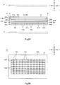
Fig. 1A is a schematic cross-sectional view of a touch sensing device according to the first embodiment of the invention. This view illustrates positional relationships between the touch sensing device, an image display device, and a polarizing plate. -
Fig. 1B is a schematic plan view of an optical laminate structure of the touch sensing device. -
Fig. 2A is a schematic cross-sectional view of a touch sensing device according to the second embodiment of the invention. This view illustrates positional relationships between the touch sensing device, an image display device, and a polarizing plate. -
Fig. 2B is a schematic plan view of an optical laminate structure of the touch sensing device. -
Fig. 3 is a schematic cross-sectional view of a touch sensing device according to the third embodiment of the invention. This view illustrates positional relationships between the touch sensing device, an image display device, and a polarizing plate. - In the brief description of the drawings above and the description of embodiments which follows, relative spatial terms such as "upper", "lower", "top", "bottom", "left", "right", "front", "rear", etc., are used for the convenience of the skilled reader and refer to the orientation of the touch sensing device, the optical laminate structure, and their constituent parts as depicted in the drawings. No limitation is intended by use of these terms, either in use of the invention, during its manufacture, shipment, custody, or sale, or during assembly of its constituent parts or when incorporated into or combined with other apparatus.
- The embodiments of the invention and their variants will now be described.
- The following describes a touch sensing device T1 according to various embodiments including the first embodiment of the invention, with reference to
Figs. 1A and 1B. Figs. 1A and 1B show the touch sensing device T1 according to the first embodiment. The touch sensing device T1 includes an optical laminate structure L1. The optical laminate structure L1 may be disposed on the front side (light emission direction side) of an image display device D, between the image display device D and the eye of the viewer, so that the viewer observes the image display device D through the optical laminate structure L1. A polarizing plate P, such as sunglasses, may be disposed between the optical laminate structure L1 and the eye of the viewer so that the image display device D is observed through the polarising plate P and the optical laminate structure L1. The image display device D displays visual information (images and text), which can be observed by a viewer either through the polarizing plate P and the optical laminate structure L1, or through only the optical laminate structure L1 without the polarizing plate P. To serve this purpose, the optical laminate structure L1 has enough optical transparency to allow visual information displayed by the image display device D to be visible to the viewer through the optical laminate structure L1 in either case. The optical laminate structure L1 may be partially or entirely transparent. The image display device D may be capable of irradiating linearly polarized light through its light source, such as an LED. Some examples of such image display devices D are liquid crystal displays (LCDs), plasma displays (PDPs), organic electroluminescent displays (OLEDs), and digital light processing (DLP) projectors. - The Z-Z' direction shown in
Fig. 1A corresponds to the thickness direction of the optical laminate structure L1. The Z direction corresponds to the direction in which the image display device D emits light (the light emission direction of the image display device D), and the Z' direction corresponds to the direction opposite to the light emission direction. The Y-Y' direction shown inFigs. 1A and 1B corresponds to the lengthwise direction of the optical laminate structure L1. The Y-Y' direction is orthogonal to the Z-Z' direction. The X-X' direction shown inFig. 1B corresponds to the widthwise direction of the optical laminate structure L1. The X-X' direction is orthogonal to the Z-Z' and Y-Y' directions. - The optical laminate structure L1 includes a
first layer 100a, asecond layer 100b, at least one step S, aretarder layer 200, a firstadhesive layer 300a, and a secondadhesive layer 300b. These components of the optical laminate structure L1 will be described below in detail. - The
first layer 100a may be an outermost layer (the outermost layer on the Z direction side in the optical laminate structure L1) of the optical laminate structure L1, such as the cover panel of the touch sensing device T1 as shown inFig. 1A . Alternatively, thefirst layer 100a may be an intermediate layer of the optical laminate structure L1. In either case, thefirst layer 100a may serve as at least one of the following functional layers: a hard coat layer, an antiglare layer, an antireflection layer, a low reflection layer, an electrode base layer, a protective layer, an anti-Newton layer, a strength retaining layer, and/or a stain-proof layer, etc. It is of course possible that thefirst layer 100a serves as a cover panel and also as at least one of the aforementioned functional layers. Thefirst layer 100a is made of plastic or like material that may cause outgassing and that has enough optical transparency to allow a user to recognize visual information displayed by the image display device D through thefirst layer 100a. For example, thefirst layer 100a may be made of polycarbonate (PC), polymethyl methacrylate (PMMA), or the like. Thefirst layer 100a may be partially or entirely transparent. Thefirst layer 100a has an outer shape and size that may be the same as, or larger than, that of thesecond layer 100b. Thefirst layer 100a may be formed by extrusion moulding, coextrusion moulding, or injection moulding or any other suitable process. - The
first layer 100a may have a retardation value in a range of 0 nm to 3,000 nm, but not limited thereto. Thefirst layer 100a may be optically isotropic. Alternatively, thefirst layer 100a may have a slow axis extending in a constant direction (e.g. the same as the slow axis direction of the retarder layer 200) and/or may have slow axes extending in any directions (i.e. randomly extending in the plane). Likewise, thefirst layer 100a may have a fast axis extending in a constant direction (e.g. the same as the fast axis direction of the retarder layer 200), or may have fast axes extending in any directions (i.e. randomly extending in the plane). Thefirst layer 100a has abonding face 101a facing thesecond layer 100b (facing in the Z' direction). - The
second layer 100b is located on the Z' direction side relative to thefirst layer 100a. Thesecond layer 100b is made of plastic or like material that has enough optical transparency to allow a user to recognize visual information displayed by the image display device D through thesecond layer 100b. For example, thesecond layer 100b may be made of polycarbonate (PC), cycloolefin polymer (COP), polyethylene terephthalate (PET), glass, or the like material. Thesecond layer 100b may be partially or entirely transparent. - The
second layer 100b may be optically isotropic. Alternatively, thesecond layer 100b may have a slow axis extending in the same direction as the slow axis direction of theretarder layer 200, and/or may have a fast axis extending in same direction as the fast axis direction of theretarder layer 200. Thesecond layer 100b has abonding face 101b facing thefirst layer 100a (facing in the Z direction). - The at least one step S is on at least one of the
bonding face 101 a of thefirst layer 100a and thebonding face 101b of thesecond layer 100b. The at least one step S may specifically have at least one of the following configurations I), II), and III). - Configuration I): The or each step S is a protrusion or recess on the
bonding face bonding face bonding face - Configuration II): The or each step S is a printed element on the
bonding face bonding face - Configuration III): The or each step S is an electrode on the
bonding face 101b of thesecond layer 100b. In this case, thesecond layer 100b serves as an electrode base layer. The electrode or electrodes will be hereinafter referred to, not as the step S, but as electrode orelectrodes 110b for convenience of description. - The at least one
electrode 110b may be configured for detecting a detection target, such as a finger or a conductor of a stylus, approaching to the outermost layer of the optical laminate structure L1, adapted to A) a surface capacitive sensing or B) a projected capacitive sensing. - In case A), a
single electrode 110b being a transparent conductive film is provided. The transparent conductive film is made of a material such as ITO (indium oxide + tin oxide) or ATO (antimony tin oxide). Also, electric field values at the four corners of the or eachelectrode 110b change in accordance with the approach of the detection target to the outermost layer. - In case B), the one or
more electrodes 110b are designed for either B1) a self capacitance sensing or B2) a mutual capacitance sensing. In either case, the one ormore electrodes 110b are made of a transparent conductive film or a conductor. The transparent conductive film may be made of a material such as tin-doped indium oxide (ITO), carbon nanotubes (CNT), indium-doped zinc oxide (IZO), aluminium-doped zinc oxide (AZO), or conductive polymer such as PEDOT and PSS. The conductor may specifically be photosensitive silver, silver nanoink, silver nanowires, vapour-deposited copper, rolled copper, copper nanoink, etc. - In the case of type B1, the one or
more electrodes 110b are configured such that when a detection target approaches theelectrode 110b or one of theelectrodes 110b, there will be a change in electrostatic capacitance generated between the approachedelectrode 110b and the detection target. The change in electrostatic capacitance changes an electric signal (voltage or current) from the approachedelectrode 110b. If a plurality ofelectrodes 110b is provided, they may preferably be spaced apart from each other on thebonding face 101b of thesecond layer 100b (seeFig. 1B ). - In the case of type B2, a plurality of
electrodes 110b are spaced apart from each other on thebonding face 101b of thesecond layer 100b. Twoadjacent electrodes 110b form a pair, one of which serves as a drive electrode, and the other of which serves as a detection electrode (sensor electrode). For example, as shown inFig. 1B , theelectrodes 110b may be arranged in four horizontal rows, in which theelectrodes 110b in the first and third rows may serve as drive electrodes, and theelectrodes 110b in the second and fourth rows may serve as detection electrodes. Alternatively, theelectrodes 110b in the first and third rows may serve as detection electrodes, and theelectrodes 110b in the second and fourth rows may serve as drive electrodes. Each two adjacent electrodes, namely drive and detection electrodes, are electrostatically coupled to each other. When a detection target approaches at least one pair of adjacent drive and detection electrodes, there will be a change in electrostatic capacitance generated between the drive and detection electrodes. The change in electrostatic capacitance changes an electric signal (voltage or current) from the detection electrode. - The
retarder layer 200 is a film or plate disposed between thefirst layer 100a and thesecond layer 100b. Theretarder layer 200 is made of a material having enough optical transparency to allow a user to recognize visual information displayed by the image display device D through theretarder layer 200. Theretarder layer 200 may be partially or entirely transparent. Theretarder layer 200 may be flexible as described below or may be rigid. The thickness (Z-Z' direction dimension) of theretarder layer 200 may fall within a range of 80 µm to 300 µm. - The
retarder layer 200 has a larger retardation value than thefirst layer 100a. For example, theretarder layer 200 may have a retardation value in the range of 3,000 nm to 30,000 nm or a retardation value of 30,000 nm or more. The slow axis of theretarder layer 200 may preferably extend at an angle of 30 to 60 degrees to the polarization axis or the absorption axis of the image display device D. Theretarder layer 200 serves to convert linearly polarized light irradiated from the image display device D into circularly polarized light (including elliptically polarized light). Generally speaking, the amount of linearly polarized light passing through a polarizing plate P varies depending on the axial relationship between the polarizing plate P and linearly polarized light, but the amount of circularly polarized light passing through a polarizing plate P does not vary. Theretarder layer 200 accordingly improves the visibility of information displayed by the image display device D through the polarizing plate P. The glass transition temperature (Tg) of theretarder layer 200 may fall within a range from -40°C to 95°C (environmental temperatures for automobile use) or within a range from - 10°C to 60°C (environmental temperatures for consumer use) or more. - The
retarder layer 200 has afirst bonding face 201 facing thefirst layer 100a (in the Z direction) and asecond bonding face 202 facing thesecond layer 100b (in the Z' direction). At least one of the first and second bonding faces 201 and 202 may or may not be surface-treated with plasma or excimer laser beams. - The first
adhesive layer 300a bonds together thebonding face 101a of thefirst layer 100a and thefirst bonding face 201 of theretarder layer 200. The firstadhesive layer 300a may specifically be an adhesive agent, an adhesive tape, such as optically clear adhesive (OCA, registered trademark), and the like. The firstadhesive layer 300a is made of a material having enough optical transparency to allow a user to recognize visual information displayed by the image display device D through the firstadhesive layer 300a. The firstadhesive layer 300a may be optically transparent. The firstadhesive layer 300a has outgassing resistance, i.e. has enough hardness to suppress outgassing from thefirst layer 100a at the interface between thebonding face 101a of thefirst layer 100a and the firstadhesive layer 300a. For example, in order to suppress outgassing from thefirst layer 100a at the interface between thebonding face 101a of thefirst layer 100a and the firstadhesive layer 300a, the firstadhesive layer 300a may preferably have a storage modulus of either 1) and 2) as follows, but is not limited thereto. - 1) storage modulus = 1 to 10 × 105 Pa (at 25°C)
- 2) storage modulus = 0.5 to 5 × 10⁵ Pa (at 80°C)
- If at least one step S is provided on the
bonding face 101a of thefirst layer 100a, the firstadhesive layer 300a is warped partially, at the portion in contact with the or each step S, so as to protrude toward the secondadhesive layer 300b. The or each warped portion of the firstadhesive layer 300a will be referred to as aprotrusion 310a. The or eachprotrusion 310a has a Z-Z' direction dimension that is 1) smaller than, or 2) approximately the same as, that of the step S. In case 1), the firstadhesive layer 300a gets distorted /dented yielding and conforming to the step S and partially absorbs the height of the step S. In case 2), theprotrusion 310a protrudes in the Z' direction, toward the secondadhesive layer 300b, by the Z-Z' direction dimension of the step S, and the firstadhesive layer 300a does not get distorted/dented conforming to the step S, i.e. does not absorb the height of the step S. Theretarder layer 200 is warped partially, at the portion in contact with the or eachprotrusion 310a, so as to protrude toward the secondadhesive layer 300b. The or each warped portion of theretarder layer 200 will be referred to as aprotrusion 210. The or eachprotrusion 210 has a Z-Z' direction dimension that is 3) smaller than, or 4) approximately the same as, that of theprotrusion 310a. In case 3), theretarder layer 200 gets distorted/dented yielding and conforming to theprotrusion 310a and partially absorbs the height of theprotrusion 310a. In case 4), theprotrusion 210 protrudes in the Z' direction, toward the secondadhesive layer 300b, by the Z-Z' direction dimension of theprotrusion 310a, and theretarder layer 200 does not does not get distorted/dented yielding and conforming to theprotrusion 310a, i.e. does not absorb the height of the step S. It should be noted that when the at least one step S is present only on thebonding face 101b of thesecond layer 100b, the firstadhesive layer 300a does not have anyprotrusions 310a, and theretarder layer 200 does not have anyprotrusions 210, either. - In addition, the first
adhesive layer 300a may have a thickness (Z-Z' direction dimension) that falls within a range of 25 to 175 µm. The firstadhesive layer 300a may have a very low retardation value, i.e. the layer may completely or nearly isotropic. For example, the retardation value of the firstadhesive layer 300a may fall within a range of 0 to 50 nm. Alternatively, the firstadhesive layer 300a may have a retardation value higher than this value range. In this case, the firstadhesive layer 300a may preferably, but not limited thereto, have a slow axis extending in the same direction to that of theretarder layer 200, or have a fast axis extending in the same direction to that of theretarder layer 200. - The second
adhesive layer 300b bonds together thebonding face 101b of thesecond layer 100b and thesecond bonding face 202 of theretarder layer 200. The secondadhesive layer 300b may specifically be an adhesive or an adhesive, such as optically clear adhesive (OCA, registered trademark) and the like. The secondadhesive layer 300b is made of a material having enough optical transparency to allow a user to recognize visual information displayed by the image display device D through the secondadhesive layer 300b. The secondadhesive layer 300b may be optically transparent. The secondadhesive layer 300b is more flexible than the firstadhesive layer 300a. Specifically, the secondadhesive layer 300b has such a hardness (step-height conformability) as to get distorted/dented yielding and conforming to the at least oneprotrusion 210 on theretarder layer 200 and/or the at least one step S on thesecond layer 100b and thereby absorb the height of the or eachprotrusion 210 of theretarder layer 200 and/or the height of the or each step S on thesecond layer 100b. In other words the second adhesive layer deforms during the lamination process to conform to the at least oneprotrusion 210 on theretarder layer 200 and/or the at least one step S on thesecond layer 100b. For example, in order to be able to get distorted/dented yielding and conforming to the at least oneprotrusion 210 and/or the at least one step S, the secondadhesive layer 300b may preferably have a storage modulus of either 1) and 2) as follows, but is not limited thereto. - 1) Second adhesive layer: storage modulus = 1 to 20 × 104 Pa (at 25°C)
- 2) Second adhesive layer: storage modulus = 1 to 10 × 104 Pa (at 80°C)
- Also, the second
adhesive layer 300b may preferably have a larger thickness (Z-Z' direction dimension) than the firstadhesive layer 300a and get distorted yielding and conforming to the shape of at least oneprotrusion 210 of theretarder layer 200 and/or the at least one step S on thesecond layer 100b. For example, the thickness of the secondadhesive layer 300b may fall within a range of 50 to 500 µm. The first and/or second adhesive layer may have a thickness greater than the height of the step in the bonding face it contacts, in order to absorb the height of the step. - The second
adhesive layer 300b may have a very low retardation value, i.e. the layer may completely or nearly isotropic. For example, the retardation value of the secondadhesive layer 300b may fall within a range of 0 to 50 nm. Alternatively, the secondadhesive layer 300b may have a retardation value higher than this value range. In this case, the secondadhesive layer 300b may preferably, but not limited thereto, have a slow axis direction that is identical to that of theretarder layer 200, or have a fast axis direction that is identical to that of theretarder layer 200. - When the or each step S on the
second layer 100b (electrode 110b) is an ITO electrode as described above, the secondadhesive layer 300b may preferably be of a material that does not contain acrylic. That is, if the or each step S on thesecond layer 100b (electrode 110b) is an electrode other than an ITO electrode or the above-described elements I) or II), the secondadhesive layer 300b may contain acrylic acid. - The touch sensing device T1 and the optical laminate structure L1 as described above has at least the following technical features. First, the touch sensing device T1 and the optical laminate structure L1 is so configured as to provide favorable visibility when viewed through them. Specifically, i) the first
adhesive layer 300a have the hardness as described above. If undesirable outgassing from thefirst layer 100a occurs at the interface between thefirst layer 100a and the firstadhesive layer 300a, the gas may expand into bubbles at the interface, causing degradation in visibility of the touch sensing device T1 and the optical laminate structure L1. However, the firstadhesive layer 300a of the above described hardness suppresses outgassing and thereby contributes to favorable visibility of the touch sensing device T1 and the optical laminate structure L1. ii) The secondadhesive layer 300b has the hardness as described above, so that the secondadhesive layer 300b gets distorted/dented following the shape of the or eachprotrusion 210 of theretarder layer 200 of thesecond layer 100b (i.e., the or each step S on thefirst layer 100a) and/or the or each step S on thesecond layer 100b to absorb the height of the or each step. In other words the second adhesive layer conforms to the contour of the or eachprotrusion 210 of theretarder layer 200 of thesecond layer 100b (i.e. the or each step S on thefirst layer 100a) and/or to the contour of the at least one step S on thesecond layer 100b. This configuration suppresses formation of bubbles into the boundary between the or each step S on thefirst layer 100a and the firstadhesive layer 300a and/or into the boundary between the or each step S on thesecond layer 100b and the secondadhesive layer 300b. Bubbles in such boundary would cause degradation in transparency of the touch sensing device T1 and the optical laminate structure L1. However, the secondadhesive layer 300b of the above described hardness suppresses formation of bubbles and thereby contributes to favorable transparency of the touch sensing device T1 and the optical laminate structure L1. iii) Theretarder layer 200, interposed between the firstadhesive layer 300a and the secondadhesive layer 300b, also contributes to favorable visibility through the touch sensing device T1 and the optical laminate structure L1 when viewed through a polarizing plate P. If thesecond layer 100b and/or the secondadhesive layer 300b have has phase-shift properties, linearly polarized light irradiated from an image display device D may be disturbed when entering thesecond layer 100b and/or the secondadhesive layer 300b. However, if thesecond layer 100b and/or the secondadhesive layer 300b are optically isotropic, or if thesecond layer 100b and/or the secondadhesive layer 300b has a slow axis or a fast axis extending in the same directions as those of theretarder layer 200, the possibility is reduced that linearly polarized light irradiated from the image display device is disturbed when entering thesecond layer 100b and/or the secondadhesive layer 300b and such disturbed light enters theretarder layer 200. Therefore, light passing through the touch sensing device T1 and the optical laminate structure L1 is linearly polarized light properly in the correct orientation, which will be properly converted into circularly polarized light. Hence, favorable visibility will be obtained even when viewed through the polarizing plate P. - Second, delamination is unlikely to occur in the touch sensing device T1 and the optical laminate structure L1 for the following reasons. Generally speaking, if the
bonding face 101a of thefirst layer 100a and thebonding face 101b of thesecond layer 100b are bonded together with an adhesive layer laminate including an adhesive layer having outgassing resistance and another adhesive layer having high step-height conformability, delamination is likely to occur between the two adhesive layers due to their low affinity. This is in contrast with the touch sensing device T1 and the optical laminate structure L1, wherein the firstadhesive layer 300a bonds thefirst layer 100a and theretarder layer 200 together, and the secondadhesive layer 300b bonds thesecond layer 100b and theretarder layer 200 together, delamination is unlikely to occur along the interface between each of the layers. In particular, if at least one of thefirst bonding face 201 and thesecond bonding face 202 of theretarder layer 200 is surface-treated with plasma or excimer laser beams, such treatment improves adhesion in the corresponding bonding part, i.e. the bonding part of theretarder layer 200 and the firstadhesive layer 300a, and the bonding part of theretarder layer 200 and the secondadhesive layer 300b. - Third, warpage is unlikely to occur in the optical laminate structure L1 for the following reasons. The optical laminate structure L1 includes two adhesive layers, namely the first
adhesive layer 300a and the secondadhesive layer 300b, so that the total thickness of the adhesive layers is increased. In addition, the secondadhesive layer 300b has high flexibility. Therefore, even if thefirst layer 100a and thesecond layer 100b thermally expand to different degrees due to their difference in thermal expansion coefficient, the difference in thermal expansion will be absorbed by the firstadhesive layer 300a and the secondadhesive layer 300b. In this case, theretarder layer 200 may preferably be a flexible film. Further advantageously, the reduced warpage in the optical laminate structure L1 contributes to reduced warping stress in the optical laminate structure L1 that would otherwise cause delamination at each interface of thefirst layer 100a, the firstadhesive layer 300a, theretarder layer 200, the secondadhesive layer 300b, and thesecond layer 100b of the optical laminate structure L1. - Fourth, if an ITO electrode is provided as a step S on the second layer 200b and if the second
adhesive layer 300b does not contain acrylic acid, the ITO electrode will not corrode on the on the second layer 200b free of acrylic acid. - Fifth, the touch sensing device T1 and the optical laminate structure L1 can be manufactured with reduced costs. This is because the
retarder layer 200 is interposed between the firstadhesive layer 300a and the secondadhesive layer 300b as described above. Therefore, there is no need to additionally provide a retarder layer for the purpose of improved visibility as viewed through a polarizing plate P. - The following describes a touch sensing device T2 according to various embodiments including the second embodiment and its variants of the invention, with reference to
Figs. 2A and 2B. Figs. 2A and 2B show the touch sensing device T2 according to the second embodiment.Fig. 2A also shows in phantom lines the polarising plate P and the display device D, in a manner similar toFig. 1A . The display device D may be viewed through only the touch sensing device T2, or may be viewed through the touch sensing device T2 and the polarising plate P, as described in relation to the previous embodiment. The touch sensing device T2 is sufficiently transparent that the information on the display device D is visible to the viewer in either case. The touch sensing device T2 includes an optical laminate structure L2. The touch sensing device T2 has the same configuration as the touch sensing device T1, except the following differences 1 to 3: - Difference 1): The optical laminate structure L2 includes a
second layer 100b' of a different configuration from that of thesecond layer 100b of the optical laminate structure L1. - Difference 2): The optical laminate structure L2 further includes a
third layer 100c and a thirdadhesive layer 300c, in addition to thefirst layer 100a, thesecond layer 100b', the at least one step S, theretarder layer 200, the firstadhesive layer 300a, and the secondadhesive layer 300b. - Difference 3): The or each step S on the
second layer 100b' has a different from configuration from that of the or each step S on thesecond layer 100b of the optical laminate structure L1. - The
third layer 100c is an electrode base layer arranged on the Z' direction side relative to thesecond layer 100b. Thethird layer 100c is made of a plastic material or the like that has enough optical transparency to allow a user to recognize visual information displayed by the image display device D through thethird layer 100c. For example, thethird layer 100c may be made of polycarbonate (PC), cycloolefin polymer (COP), polyethylene terephthalate (PET), glass, or the like material. Thethird layer 100c may be partially or entirely transparent. Thethird layer 100c may be optically isotropic, or alternatively thethird layer 100c may have a slow axis extending in the same direction as the slow axis direction of theretarder layer 200 or a fast axis extending in the same direction as the fast axis direction of theretarder layer 200. - The
third layer 100c has abonding face 101c facing thesecond layer 100b (facing in the Z direction). On thebonding face 101c of thethird layer 100c, a plurality ofelectrodes 110c is arranged in spaced relation to each other in the Y-Y' direction. Theelectrodes 110c extend in the X-X' direction. It should be noted that on thebonding face 101c of thethird layer 100c, there may also be at least one step, which or each of which may be anelectrode 110c or may have the same configuration as that of the at least one step S on thesecond layer 100b'. - The
second layer 100b' has the same configuration as that of thesecond layer 100b, except that thesecond layer 100b' further includes abonding face 102b'. Thebonding face 102b' of thesecond layer 100b' faces thethird layer 100c, i.e., faces in the Z' direction. - The at least one step S of the optical laminate structure L2 is provided on the
bonding face 101a of thefirst layer 100a and/or on thebonding face 101b' of thesecond layer 100b'. The step S may be at least one of the following configurations I), II), and III). Configuration I): The or each step S of the optical laminate structure L2 has the same configuration as Configuration I) of the or each step S of the optical laminate structure L1. Configuration II): The or each step S of the optical laminate structure L2 has the same configuration as Configuration II) of the or each step S of the optical laminate structure L1. - Configuration III): The at least one step S on the
second layer 100b' of the optical laminate structure L2 is a plurality of electrodes arranged in spaced relation to each other in the X-X' direction on thebonding face 101b' of thesecond layer 100b'. The electrodes extend in the Y-Y' direction. The electrodes will be hereinafter referred to, not as the step S, as electrode orelectrodes 110b' for convenience of description. Thesecond layer 100b', having theelectrodes 110b' thereon, serves as an electrode base layer. - The
electrodes 110b' and theelectrodes 110c adapted to a mutual capacitive sensing. Theelectrodes 110b' cross theelectrodes 110c at right angles or at other angles, at a different height level in the Z-Z' direction from theelectrodes 110c. Theelectrodes 110b' may be drive electrodes and theelectrodes 110c may be detection electrodes (sensor electrodes). Alternatively, theelectrodes 110b' may be are detection electrodes (sensor electrodes) and theelectrodes 110c may be drive electrodes. Theelectrodes 110b' and 110c are transparent conductive films or conductors. Specifically, the transparent conductive films may be made of a material such as tin-doped indium oxide (ITO), carbon nanotubes (CNT), indium-doped zinc oxide (IZO), aluminium-doped zinc oxide (AZO), or conductive polymer such as PEDOT and PSS. The conductors may specifically be photosensitive silver, metal (for example, Ag or Cu) with a line width of 15 µm or less formed by graph offset or other method, silver nanoink, silver nanowires, metal wires, vapour deposited copper, rolled copper, copper nanoink, or the like. Each drive electrode is electrostatically coupled to a respective detection electrode crossing the drive electrode. Accordingly, when a detection target approaches at least one pair of intersecting drive and detection electrodes, there is a change in electrostatic capacitance between the drive and detection electrodes, and the change in the electrostatic capacitance changes the electric signal from the detection electrode (voltage or current). It should be noted that theelectrodes 110b' and 110c may be rhombic electrodes and may be adapted to a self capacitance sensing. - The third
adhesive layer 300c be of any configuration that is capable of bonding together thebonding face 102b' of thesecond layer 100b and thebonding face 101c of thethird layer 100c. The thirdadhesive layer 300c may have the same configuration as the secondadhesive layer 300b. In this case, the thirdadhesive layer 300c has such a hardness (step-height conformability) as to get distorted/dented yielding and conforming to the at least one step, such as theelectrodes 110c, on thethird layer 100c. - It should be noted that the
third layer 100c and the thirdadhesive layer 300c may be omitted. In this case, theelectrodes 110c may preferably be provided on thebonding face 102b' of thesecond layer 100b', not on thebonding face 101c of thethird layer 100c so as to be spaced apart from each other in the Y-Y' direction. Except this modification, theelectrodes 110c are configured as described above. - The touch sensing device T2 and the optical laminate structure L2 configured as described above have various technical features, at least ones similar to the first to fifth technical features of the touch sensing device T1 and the optical laminate structure L1.
- The following describes a touch sensing device T3 according to various embodiments including the third embodiment of the invention, with reference to
Fig. 3. Fig. 3 shows the touch sensing device T3 according to the third embodiment.Fig. 3 also shows in phantom lines the polarising plate P and the display device D, in a manner similar toFigs. 1A and2A . The display device D may be viewed through only the touch sensing device T3, or may be viewed through the touch sensing device T3 and the polarising plate P, as described in relation to the previous embodiments. The touch sensing device T3 is sufficiently transparent that the information on the display device D is visible to the viewer in either case. The touch sensing device T3 includes an optical laminate structure L3. The touch sensing device T3 has the same configuration as the touch sensing device T1, except that thesecond layer 100b of the optical laminate structure L3 has at least one step S which or each of which has a different configuration from that of the or each step S on thesecond layer 100b of the optical laminate structure L1. This difference will be described in detail, without repeating descriptions on the touch sensing device T3 that overlap with those of the touch sensing device T1. It should be noted thatFig. 3 shows the Z-Z' and Y-Y' directions in a similar manner toFig. 1A . There is no figure showing the X-X' direction for this embodiment, the Z-Z', Y-Y', and X-X' directions are defined as described for the first embodiment. - The at least one step S of the optical laminate structure L3 is provided on the
bonding face 101a of thefirst layer 100a and/or on thebonding face 101b of thesecond layer 100b. The step S may be at least one of the following configurations I), II), and III). - Configuration I): The or each step S of the optical laminate structure L3 has the same configuration as Configuration I) of the or each step S of the optical laminate structure L1.
- Configuration II): The or each step S of the optical laminate structure L3 has the same configuration as Configuration II) of the or each step S of the optical laminate structure L1.
- Configuration III): The at least one step S on the
second layer 100b of the optical laminate structure L3 includesfirst electrodes 111b,second electrodes 112b, and an insulatinglayer 113b. Thefirst electrodes 111b are so arranged on thebonding face 101b of thesecond layer 100b as to extend in the X-X' direction in spaced relation to each other in the Y-Y' direction. The insulatinglayer 113b is disposed on thebonding face 101b of thesecond layer 100b in such a manner as to cover thefirst electrodes 111b. Thesecond electrodes 112b are so arranged on the insulatinglayer 113b as to extend in the Y-Y' direction in spaced relation to each other each other in the X-X' direction. Other than these, thefirst electrode 111b and thesecond electrode 112b may have the same configurations as theelectrode 110c and theelectrode 110b', respectively, of the optical laminate structure L2. - When the at least one step S on the
second layer 100b of the optical laminate structure L3 includes steps of Configuration III) above, the secondadhesive layer 300b may have a thickness (Z-Z' direction dimension) that is larger than the thickness of the secondadhesive layer 300b of the optical laminate structure L1 or the optical laminate structure L2. For example, the thickness of the secondadhesive layer 300b of the optical laminate structure L3 may fall within a range of 50 to 500 µm. It is of course possible that the secondadhesive layer 300b of the optical laminate structure L3 has the same thickness as the secondadhesive layer 300b of the optical laminate structure L1 or the optical laminate structure L2. If thefirst electrodes 111b or the second electrodes, i.e. the at least one step S, are ITO electrodes, the secondadhesive layer 300b of the optical laminate structure L3 may be of a material that does not contain acrylic acid. - The touch sensing device T3 and the optical laminate structure L3 configured as described above have various technical features, at least ones similar to the first to fifth technical features of the touch sensing device T1 and the optical laminate structure L1.
- It should be noted that the above-described touch sensing device and optical laminate structure of the invention are not limited to the embodiments and their variants described above and may be modified in any manner within the scope of the claims. Some modification examples will be described below.
- The optical laminate structure of the invention may be installed is a touch sensing device as described above, but it is not limited thereto. The optical laminate structure of the invention may be any structure that allows a user to recognize visual information displayed by an image display device through the optical laminate structure. If the optical laminate structure of the invention is installed in a device other than a touch sensing device, the or each step on the bonding face of the second layer may be any one of the configurations I) and II) or may be an electrode for other device than a touch sensing device (e.g. a sensor electrode).
- It should be appreciated that the touch sensing device and the optical laminate structure of the above embodiments and variants thereof are described above by way of examples only. The Z-Z' direction of the invention may be any direction as long as it is the thickness direction of the optical laminate structure and the lamination direction of the layers of the optical laminate structure. The Y-Y' direction of the invention may be any direction crossing the Z-Z' direction. The X-X' direction of the invention may be any direction crossing the Z-Z' and Y-Y' directions and being located in a different plane from the plane defined by the Z-Z' and Y-Y' directions.
-
- T1: touch sensing device
- L1: optical laminate structure
- 100a: first layer
- 101a: bonding face
- 100b: second layer
- 101b: bonding face
- 110b: electrode
- S: step
- 200: retarder layer
- 201: first bonding face
- 202: second bonding face
- 210: protrusion
- 300a: first adhesive layer
- 310a: protrusion
- 300b: second adhesive layer
- 100a: first layer
- L1: optical laminate structure
- T2: touch sensing device
- L2: optical laminate structure
- 100a: first layer
- 101a: bonding face
- 100b': second layer
- 101b': bonding face
- 110b': electrode
- 102b': bonding face
- 100c: third layer
- 101c: bonding face
- 110c: electrode
- S: step
- 200: retarder layer
- 201: first bonding face
- 202: second bonding face
- 210: protrusion
- 300a: first adhesive layer
- 310a: protrusion
- 300b: second adhesive layer
- 300c: third adhesive layer
- 100a: first layer
- L2: optical laminate structure
- T3: touch sensing device
- L3: optical laminate structure
- 100a: first layer
- 101a: bonding face
- 100b: second layer
- 101b: bonding face
- S: step
- 111b: first electrode
- 112b: second electrode
- 113b: insulating layer
- 200: retarder layer
- 201: first bonding face
- 202: second bonding face
- 210: protrusion
- 300a: first adhesive layer
- 310a: protrusion
- 300b: second adhesive layer
- 100a: first layer
- L3: optical laminate structure
- D: image display device
- P: polarizing plate.
Claims (15)
- An optical laminate structure (L1, L2, L3) comprising:a first layer (100a) made of a material that may cause outgassing, the first layer having a bonding face (101a);a second layer (100b) having a bonding face (101b);at least one step (S) on at least one of the bonding faces (101a, 101b) of the first (100a) and second (100b) layers;a retarder layer (200) between the first layer (100a) and the second layer (100b), the retarder layer having a first bonding face (201) facing the first layer (100a) and a second bonding face (202) facing the second layer (100b);a first adhesive layer (300a) bonding together the bonding face (101a) of the first layer (100a) and the first bonding face (201) of the retarder layer (200), the first adhesive layer having such hardness that suppresses the outgassing in an interface between the first layer (100a) and the first adhesive layer (300a); anda second adhesive layer (300b) bonding together the bonding face (101b) of the second layer (100b) and the second bonding face (202) of the retarder layer (200), the second adhesive layer being more flexible than the first adhesive layer (300a), the second adhesive layer (300b) having such hardness as to get distorted by the step (S) and thereby absorb height of the step (S).
- An optical laminate structure (L1, L2, L3) according to claim 1 wherein the optical transparency of the optical laminate structure is such as to allow a user to recognize visual information displayed by an image display device (D) through the optical laminate structure.
- The optical laminate structure (L1, L2, L3) according to claim 1 or claim 2,
wherein the first layer (100a) has a retardation value in a range of 0 nm to 3,000 nm, and
wherein the retarder layer (200) has a retardation value in a range of 3,000 nm to 30,000 nm. - The optical laminate structure (L1, L2, L3) according to any one of claims 1 to 3, wherein at least one of the first (201) and second (202) bonding faces of the retarder layer (200) is surface-treated with plasma or excimer laser beams.
- The optical laminate structure (L1, L2, L3) according to any one of claims 1 to 4, wherein the at least one step (S) is at least one of:a protrusion or recess in the bonding face of the first (100a) or second (100b) layer,a printed element on the bonding face of the first (100a) or second (100b) layer, andan electrode on the bonding face (101b) of the second (100b) layer.
- The optical laminate structure (L1, L2, L3) according to any one of claims 1 to 5, wherein the second layer (100b) is optically isotropic.
- The optical laminate structure (L1, L2, L3) according to any one of claims 1 to 5, wherein the second layer (100b) has a slow axis extending in a direction that is substantially equal to a direction of a slow axis of the retarder layer (200) or has a fast axis extending in a direction that is substantially equal to a direction of a fast axis of the retarder layer (200).
- The optical laminate structure (L1, L2, L3) according to any one of claims 1 to 7, wherein
the at least one step (S) comprises a plurality of steps (S),
at least one (S) of the steps is provided on the bonding face (101a) of the first layer (100a),
the remaining step or steps (S) are provided on the bonding face (101b) of the second layer (100b), and
the second layer is distorted by the steps (S) on the first (100a) and second (100b) layers and thereby absorbs height of the steps. - The optical laminate structure (L1, L2, L3) according to any one of claims 1 to 8, wherein the second adhesive layer (300b) has a thickness that is larger than the first adhesive layer (300a) and that is adapted to get distorted by the at least one step (S).
- The optical laminate structure (L1, L2, L3) according to any one of claims 1 to 9, wherein the first adhesive layer (300a) has a retardation value within a range of 0 to 50 nm.
- The optical laminate structure (L1, L2, L3) according to any one of claims 1 to 9, wherein the first adhesive layer (300a) has a slow axis extending in a direction that is substantially equal to a direction of a slow axis of the retarder layer (200), or has a fast axis extending in a direction that is substantially equal to a direction of a fast axis of the retarder layer (200).
- The optical laminate structure (L1, L2, L3) according to any one of claims 1 to 11, wherein the second adhesive layer (300b) has a retardation value within a range of 0 to 50 nm.
- The optical laminate structure (L1, L2, L3) according to any one of claims 1 to 11, wherein the second adhesive layer (300b) has a slow axis extending in a direction that is substantially equal to a direction of a slow axis of the retarder layer (200), or the second adhesive layer has a fast axis extending in a direction that is substantially equal to a direction of a fast axis of the retarder layer (200).
- A touch sensing device (T1, T2, T3) comprising the optical laminate structure (L1, L2, L3) according to any one of claims 1 to 13.
- The touch sensing device (T1, T2, T3) according to claim 14, wherein
the at least one step (S) includes an ITO electrode on the bonding face (101b) of the second layer (100b), and
the second adhesive layer (300b) does not contain acrylic acid.
Applications Claiming Priority (1)
| Application Number | Priority Date | Filing Date | Title |
|---|---|---|---|
| JP2016181521A JP6732614B2 (en) | 2016-09-16 | 2016-09-16 | Optical laminate and touch input device including the same |
Publications (2)
| Publication Number | Publication Date |
|---|---|
| EP3296776A1 true EP3296776A1 (en) | 2018-03-21 |
| EP3296776B1 EP3296776B1 (en) | 2020-07-29 |
Family
ID=59699446
Family Applications (1)
| Application Number | Title | Priority Date | Filing Date |
|---|---|---|---|
| EP17020368.1A Active EP3296776B1 (en) | 2016-09-16 | 2017-08-21 | Optical laminate structure and touch sensing device having the same |
Country Status (6)
| Country | Link |
|---|---|
| US (1) | US10723101B2 (en) |
| EP (1) | EP3296776B1 (en) |
| JP (1) | JP6732614B2 (en) |
| KR (1) | KR102412795B1 (en) |
| CN (1) | CN107831934B (en) |
| TW (1) | TWI729147B (en) |
Families Citing this family (6)
| Publication number | Priority date | Publication date | Assignee | Title |
|---|---|---|---|---|
| JP6579254B1 (en) | 2018-12-03 | 2019-09-25 | 王子ホールディングス株式会社 | Laminate and method for producing laminate |
| CN113486801B (en) * | 2020-08-17 | 2023-05-23 | 友达光电股份有限公司 | Sensing device |
| CN114327120A (en) * | 2020-09-30 | 2022-04-12 | 宸鸿科技(厦门)有限公司 | Curved surface structure, manufacturing method thereof and display device |
| KR20230018856A (en) * | 2021-07-30 | 2023-02-07 | 삼성전자주식회사 | Electronic device including digitizer |
| US12481093B2 (en) | 2022-06-24 | 2025-11-25 | 3M Innovative Properties Company | Low-emissivity film for article of personal protective equipment |
| TWI841311B (en) * | 2023-03-22 | 2024-05-01 | 致伸科技股份有限公司 | Touch pad module |
Citations (5)
| Publication number | Priority date | Publication date | Assignee | Title |
|---|---|---|---|---|
| US20090022967A1 (en) * | 2005-04-13 | 2009-01-22 | Mitsubishi Plastics, Inc. | Double sided adhesive sheet and panel laminate |
| WO2010044229A1 (en) | 2008-10-15 | 2010-04-22 | 三菱樹脂株式会社 | Transparent adhesive sheet and image display device |
| JP2012017386A (en) | 2010-07-07 | 2012-01-26 | Dic Corp | Double-sided pressure-sensitive adhesive tape for panel fixing |
| US20120062823A1 (en) * | 2009-06-01 | 2012-03-15 | Sharp Kabushiki Kaisha | Liquid crystal display device |
| EP2869099A1 (en) * | 2013-02-07 | 2015-05-06 | Nitto Denko Corporation | Optical laminate having polarizing film |
Family Cites Families (17)
| Publication number | Priority date | Publication date | Assignee | Title |
|---|---|---|---|---|
| JP2000111896A (en) * | 1998-08-04 | 2000-04-21 | Kanegafuchi Chem Ind Co Ltd | Liquid crystal display device with touch panel and touch panel |
| CN1296732C (en) * | 2002-04-23 | 2007-01-24 | 日东电工株式会社 | Polarization member, polarized light source and image display device using the same |
| CN101258432A (en) * | 2005-09-09 | 2008-09-03 | 日东电工株式会社 | Polarizing plate with optical compensation layer, liquid crystal panel using polarizing plate with optical compensation layer, and image display device |
| JP2007248837A (en) * | 2006-03-16 | 2007-09-27 | Fujifilm Corp | Optically anisotropic film, optical compensation sheet, polarizing plate using the same, transfer material, and liquid crystal display device |
| JP5529720B2 (en) * | 2010-12-15 | 2014-06-25 | 日東電工株式会社 | Transparent conductive film with pressure-sensitive adhesive layer, method for producing the same, and touch panel |
| JP2012237928A (en) * | 2011-05-13 | 2012-12-06 | Fujifilm Corp | Optical film, polarizing plate, image display device and three-dimensional image display system |
| JP5512624B2 (en) * | 2011-09-21 | 2014-06-04 | 日本写真印刷株式会社 | Capacitive touch sensor and display device having the same |
| US9441141B2 (en) * | 2012-01-18 | 2016-09-13 | Mitsubishi Plastics, Inc. | Transparent double-sided adhesive sheet for image display device and image display device using the same |
| KR20140042517A (en) * | 2012-09-28 | 2014-04-07 | 삼성디스플레이 주식회사 | Polarizing adhesive element, method of manufacturing the same and display apparatus having the same |
| JP6136526B2 (en) * | 2012-10-29 | 2017-05-31 | 大日本印刷株式会社 | Optical laminate for front surface of in-cell touch panel liquid crystal element and in-cell touch panel type liquid crystal display device using the same |
| JP6275945B2 (en) * | 2012-12-10 | 2018-02-07 | 日東電工株式会社 | Optical film with double-sided pressure-sensitive adhesive, and method for manufacturing an image display device using the same |
| JP6663628B2 (en) * | 2013-07-31 | 2020-03-13 | 日東電工株式会社 | Adhesive sheet, optical film with adhesive layer, and image display device |
| KR20150015314A (en) * | 2013-07-31 | 2015-02-10 | 제일모직주식회사 | Transparent conductor and optical display apparatus comprising the same |
| JP6192465B2 (en) | 2013-09-27 | 2017-09-06 | ホシデン株式会社 | Touch panel and display device |
| US10073569B2 (en) * | 2014-01-28 | 2018-09-11 | Apple Inc. | Integrated polarizer and conductive material |
| JP6580315B2 (en) * | 2014-10-15 | 2019-09-25 | 日東電工株式会社 | Optical film with double-sided pressure-sensitive adhesive, method for producing image display device using the same, and curl suppression method for optical film with double-sided pressure-sensitive adhesive |
| JP6456686B2 (en) * | 2014-12-25 | 2019-01-23 | 日東電工株式会社 | Polarizing film with adhesive layer and image display device |
-
2016
- 2016-09-16 JP JP2016181521A patent/JP6732614B2/en active Active
-
2017
- 2017-06-02 TW TW106118319A patent/TWI729147B/en active
- 2017-06-16 KR KR1020170076834A patent/KR102412795B1/en active Active
- 2017-08-21 EP EP17020368.1A patent/EP3296776B1/en active Active
- 2017-08-28 US US15/688,615 patent/US10723101B2/en active Active
- 2017-09-11 CN CN201710810532.5A patent/CN107831934B/en active Active
Patent Citations (5)
| Publication number | Priority date | Publication date | Assignee | Title |
|---|---|---|---|---|
| US20090022967A1 (en) * | 2005-04-13 | 2009-01-22 | Mitsubishi Plastics, Inc. | Double sided adhesive sheet and panel laminate |
| WO2010044229A1 (en) | 2008-10-15 | 2010-04-22 | 三菱樹脂株式会社 | Transparent adhesive sheet and image display device |
| US20120062823A1 (en) * | 2009-06-01 | 2012-03-15 | Sharp Kabushiki Kaisha | Liquid crystal display device |
| JP2012017386A (en) | 2010-07-07 | 2012-01-26 | Dic Corp | Double-sided pressure-sensitive adhesive tape for panel fixing |
| EP2869099A1 (en) * | 2013-02-07 | 2015-05-06 | Nitto Denko Corporation | Optical laminate having polarizing film |
Also Published As
| Publication number | Publication date |
|---|---|
| JP6732614B2 (en) | 2020-07-29 |
| US20180079933A1 (en) | 2018-03-22 |
| EP3296776B1 (en) | 2020-07-29 |
| KR102412795B1 (en) | 2022-06-24 |
| TWI729147B (en) | 2021-06-01 |
| CN107831934B (en) | 2022-04-29 |
| CN107831934A (en) | 2018-03-23 |
| JP2018045567A (en) | 2018-03-22 |
| KR20180030750A (en) | 2018-03-26 |
| TW201823948A (en) | 2018-07-01 |
| US10723101B2 (en) | 2020-07-28 |
Similar Documents
| Publication | Publication Date | Title |
|---|---|---|
| EP3296776B1 (en) | Optical laminate structure and touch sensing device having the same | |
| CN108509096B (en) | High performance touch sensor and method of manufacturing the same | |
| US9939974B2 (en) | Contact sensitive display device with thin profile and low external light reflectivity | |
| US9719770B2 (en) | Touchscreen sensor | |
| JP5512624B2 (en) | Capacitive touch sensor and display device having the same | |
| TW201808630A (en) | Resin laminate and touch input device having the same | |
| KR102047504B1 (en) | Touch Sensor and Display Device Including the Same | |
| EP2772839A2 (en) | Touch panel | |
| US10095333B2 (en) | Touch apparatus | |
| US10331254B2 (en) | Touch organic light-emitting diode display device and touch device | |
| KR101401050B1 (en) | Touch sensing electrode and touch screen panel comprising the same | |
| US10338748B1 (en) | Reduction of touch sensor pattern visibility using beamsplitters | |
| US20240308181A1 (en) | Flexible display device and upper film therefor | |
| EP2808731A2 (en) | Display device comprising protective films | |
| KR20190022313A (en) | Resin laminate and touch input device having the same | |
| KR102497657B1 (en) | Display device | |
| JP6384177B2 (en) | Touch panel sensor, touch panel device, and display device | |
| US10809859B2 (en) | Capacitive sensor | |
| JP2016194746A (en) | Intermediate member for touch panel sensor, and manufacturing method of touch panel sensor | |
| US20260114157A1 (en) | Display device | |
| WO2019044155A1 (en) | Input device | |
| JP2014235684A (en) | Transparent planar body and transparent touch panel |
Legal Events
| Date | Code | Title | Description |
|---|---|---|---|
| PUAI | Public reference made under article 153(3) epc to a published international application that has entered the european phase |
Free format text: ORIGINAL CODE: 0009012 |
|
| STAA | Information on the status of an ep patent application or granted ep patent |
Free format text: STATUS: THE APPLICATION HAS BEEN PUBLISHED |
|
| AK | Designated contracting states |
Kind code of ref document: A1 Designated state(s): AL AT BE BG CH CY CZ DE DK EE ES FI FR GB GR HR HU IE IS IT LI LT LU LV MC MK MT NL NO PL PT RO RS SE SI SK SM TR |
|
| AX | Request for extension of the european patent |
Extension state: BA ME |
|
| STAA | Information on the status of an ep patent application or granted ep patent |
Free format text: STATUS: REQUEST FOR EXAMINATION WAS MADE |
|
| 17P | Request for examination filed |
Effective date: 20180810 |
|
| RBV | Designated contracting states (corrected) |
Designated state(s): AL AT BE BG CH CY CZ DE DK EE ES FI FR GB GR HR HU IE IS IT LI LT LU LV MC MK MT NL NO PL PT RO RS SE SI SK SM TR |
|
| STAA | Information on the status of an ep patent application or granted ep patent |
Free format text: STATUS: EXAMINATION IS IN PROGRESS |
|
| 17Q | First examination report despatched |
Effective date: 20190516 |
|
| GRAP | Despatch of communication of intention to grant a patent |
Free format text: ORIGINAL CODE: EPIDOSNIGR1 |
|
| STAA | Information on the status of an ep patent application or granted ep patent |
Free format text: STATUS: GRANT OF PATENT IS INTENDED |
|
| INTG | Intention to grant announced |
Effective date: 20200318 |
|
| GRAS | Grant fee paid |
Free format text: ORIGINAL CODE: EPIDOSNIGR3 |
|
| GRAA | (expected) grant |
Free format text: ORIGINAL CODE: 0009210 |
|
| STAA | Information on the status of an ep patent application or granted ep patent |
Free format text: STATUS: THE PATENT HAS BEEN GRANTED |
|
| AK | Designated contracting states |
Kind code of ref document: B1 Designated state(s): AL AT BE BG CH CY CZ DE DK EE ES FI FR GB GR HR HU IE IS IT LI LT LU LV MC MK MT NL NO PL PT RO RS SE SI SK SM TR |
|
| REG | Reference to a national code |
Ref country code: CH Ref legal event code: EP |
|
| REG | Reference to a national code |
Ref country code: AT Ref legal event code: REF Ref document number: 1296453 Country of ref document: AT Kind code of ref document: T Effective date: 20200815 |
|
| REG | Reference to a national code |
Ref country code: IE Ref legal event code: FG4D |
|
| REG | Reference to a national code |
Ref country code: DE Ref legal event code: R096 Ref document number: 602017020372 Country of ref document: DE |
|
| REG | Reference to a national code |
Ref country code: NL Ref legal event code: FP |
|
| REG | Reference to a national code |
Ref country code: LT Ref legal event code: MG4D |
|
| REG | Reference to a national code |
Ref country code: AT Ref legal event code: MK05 Ref document number: 1296453 Country of ref document: AT Kind code of ref document: T Effective date: 20200729 |
|
| PG25 | Lapsed in a contracting state [announced via postgrant information from national office to epo] |
Ref country code: GR Free format text: LAPSE BECAUSE OF FAILURE TO SUBMIT A TRANSLATION OF THE DESCRIPTION OR TO PAY THE FEE WITHIN THE PRESCRIBED TIME-LIMIT Effective date: 20201030 Ref country code: LT Free format text: LAPSE BECAUSE OF FAILURE TO SUBMIT A TRANSLATION OF THE DESCRIPTION OR TO PAY THE FEE WITHIN THE PRESCRIBED TIME-LIMIT Effective date: 20200729 Ref country code: FI Free format text: LAPSE BECAUSE OF FAILURE TO SUBMIT A TRANSLATION OF THE DESCRIPTION OR TO PAY THE FEE WITHIN THE PRESCRIBED TIME-LIMIT Effective date: 20200729 Ref country code: AT Free format text: LAPSE BECAUSE OF FAILURE TO SUBMIT A TRANSLATION OF THE DESCRIPTION OR TO PAY THE FEE WITHIN THE PRESCRIBED TIME-LIMIT Effective date: 20200729 Ref country code: NO Free format text: LAPSE BECAUSE OF FAILURE TO SUBMIT A TRANSLATION OF THE DESCRIPTION OR TO PAY THE FEE WITHIN THE PRESCRIBED TIME-LIMIT Effective date: 20201029 Ref country code: ES Free format text: LAPSE BECAUSE OF FAILURE TO SUBMIT A TRANSLATION OF THE DESCRIPTION OR TO PAY THE FEE WITHIN THE PRESCRIBED TIME-LIMIT Effective date: 20200729 Ref country code: BG Free format text: LAPSE BECAUSE OF FAILURE TO SUBMIT A TRANSLATION OF THE DESCRIPTION OR TO PAY THE FEE WITHIN THE PRESCRIBED TIME-LIMIT Effective date: 20201029 Ref country code: PT Free format text: LAPSE BECAUSE OF FAILURE TO SUBMIT A TRANSLATION OF THE DESCRIPTION OR TO PAY THE FEE WITHIN THE PRESCRIBED TIME-LIMIT Effective date: 20201130 Ref country code: SE Free format text: LAPSE BECAUSE OF FAILURE TO SUBMIT A TRANSLATION OF THE DESCRIPTION OR TO PAY THE FEE WITHIN THE PRESCRIBED TIME-LIMIT Effective date: 20200729 Ref country code: HR Free format text: LAPSE BECAUSE OF FAILURE TO SUBMIT A TRANSLATION OF THE DESCRIPTION OR TO PAY THE FEE WITHIN THE PRESCRIBED TIME-LIMIT Effective date: 20200729 |
|
| PG25 | Lapsed in a contracting state [announced via postgrant information from national office to epo] |
Ref country code: PL Free format text: LAPSE BECAUSE OF FAILURE TO SUBMIT A TRANSLATION OF THE DESCRIPTION OR TO PAY THE FEE WITHIN THE PRESCRIBED TIME-LIMIT Effective date: 20200729 Ref country code: RS Free format text: LAPSE BECAUSE OF FAILURE TO SUBMIT A TRANSLATION OF THE DESCRIPTION OR TO PAY THE FEE WITHIN THE PRESCRIBED TIME-LIMIT Effective date: 20200729 Ref country code: LV Free format text: LAPSE BECAUSE OF FAILURE TO SUBMIT A TRANSLATION OF THE DESCRIPTION OR TO PAY THE FEE WITHIN THE PRESCRIBED TIME-LIMIT Effective date: 20200729 Ref country code: IS Free format text: LAPSE BECAUSE OF FAILURE TO SUBMIT A TRANSLATION OF THE DESCRIPTION OR TO PAY THE FEE WITHIN THE PRESCRIBED TIME-LIMIT Effective date: 20201129 |
|
| REG | Reference to a national code |
Ref country code: CH Ref legal event code: PL |
|
| PG25 | Lapsed in a contracting state [announced via postgrant information from national office to epo] |
Ref country code: IT Free format text: LAPSE BECAUSE OF FAILURE TO SUBMIT A TRANSLATION OF THE DESCRIPTION OR TO PAY THE FEE WITHIN THE PRESCRIBED TIME-LIMIT Effective date: 20200729 Ref country code: EE Free format text: LAPSE BECAUSE OF FAILURE TO SUBMIT A TRANSLATION OF THE DESCRIPTION OR TO PAY THE FEE WITHIN THE PRESCRIBED TIME-LIMIT Effective date: 20200729 Ref country code: SM Free format text: LAPSE BECAUSE OF FAILURE TO SUBMIT A TRANSLATION OF THE DESCRIPTION OR TO PAY THE FEE WITHIN THE PRESCRIBED TIME-LIMIT Effective date: 20200729 Ref country code: LI Free format text: LAPSE BECAUSE OF NON-PAYMENT OF DUE FEES Effective date: 20200831 Ref country code: LU Free format text: LAPSE BECAUSE OF NON-PAYMENT OF DUE FEES Effective date: 20200821 Ref country code: RO Free format text: LAPSE BECAUSE OF FAILURE TO SUBMIT A TRANSLATION OF THE DESCRIPTION OR TO PAY THE FEE WITHIN THE PRESCRIBED TIME-LIMIT Effective date: 20200729 Ref country code: CZ Free format text: LAPSE BECAUSE OF FAILURE TO SUBMIT A TRANSLATION OF THE DESCRIPTION OR TO PAY THE FEE WITHIN THE PRESCRIBED TIME-LIMIT Effective date: 20200729 Ref country code: CH Free format text: LAPSE BECAUSE OF NON-PAYMENT OF DUE FEES Effective date: 20200831 Ref country code: DK Free format text: LAPSE BECAUSE OF FAILURE TO SUBMIT A TRANSLATION OF THE DESCRIPTION OR TO PAY THE FEE WITHIN THE PRESCRIBED TIME-LIMIT Effective date: 20200729 |
|
| REG | Reference to a national code |
Ref country code: DE Ref legal event code: R097 Ref document number: 602017020372 Country of ref document: DE |
|
| REG | Reference to a national code |
Ref country code: BE Ref legal event code: MM Effective date: 20200831 |
|
| PG25 | Lapsed in a contracting state [announced via postgrant information from national office to epo] |
Ref country code: AL Free format text: LAPSE BECAUSE OF FAILURE TO SUBMIT A TRANSLATION OF THE DESCRIPTION OR TO PAY THE FEE WITHIN THE PRESCRIBED TIME-LIMIT Effective date: 20200729 |
|
| PLBE | No opposition filed within time limit |
Free format text: ORIGINAL CODE: 0009261 |
|
| STAA | Information on the status of an ep patent application or granted ep patent |
Free format text: STATUS: NO OPPOSITION FILED WITHIN TIME LIMIT |
|
| PG25 | Lapsed in a contracting state [announced via postgrant information from national office to epo] |
Ref country code: SK Free format text: LAPSE BECAUSE OF FAILURE TO SUBMIT A TRANSLATION OF THE DESCRIPTION OR TO PAY THE FEE WITHIN THE PRESCRIBED TIME-LIMIT Effective date: 20200729 |
|
| 26N | No opposition filed |
Effective date: 20210430 |
|
| PG25 | Lapsed in a contracting state [announced via postgrant information from national office to epo] |
Ref country code: BE Free format text: LAPSE BECAUSE OF NON-PAYMENT OF DUE FEES Effective date: 20200831 Ref country code: SI Free format text: LAPSE BECAUSE OF FAILURE TO SUBMIT A TRANSLATION OF THE DESCRIPTION OR TO PAY THE FEE WITHIN THE PRESCRIBED TIME-LIMIT Effective date: 20200729 Ref country code: IE Free format text: LAPSE BECAUSE OF NON-PAYMENT OF DUE FEES Effective date: 20200821 |
|
| PG25 | Lapsed in a contracting state [announced via postgrant information from national office to epo] |
Ref country code: TR Free format text: LAPSE BECAUSE OF FAILURE TO SUBMIT A TRANSLATION OF THE DESCRIPTION OR TO PAY THE FEE WITHIN THE PRESCRIBED TIME-LIMIT Effective date: 20200729 Ref country code: MT Free format text: LAPSE BECAUSE OF FAILURE TO SUBMIT A TRANSLATION OF THE DESCRIPTION OR TO PAY THE FEE WITHIN THE PRESCRIBED TIME-LIMIT Effective date: 20200729 Ref country code: CY Free format text: LAPSE BECAUSE OF FAILURE TO SUBMIT A TRANSLATION OF THE DESCRIPTION OR TO PAY THE FEE WITHIN THE PRESCRIBED TIME-LIMIT Effective date: 20200729 |
|
| PG25 | Lapsed in a contracting state [announced via postgrant information from national office to epo] |
Ref country code: MK Free format text: LAPSE BECAUSE OF FAILURE TO SUBMIT A TRANSLATION OF THE DESCRIPTION OR TO PAY THE FEE WITHIN THE PRESCRIBED TIME-LIMIT Effective date: 20200729 Ref country code: MC Free format text: LAPSE BECAUSE OF FAILURE TO SUBMIT A TRANSLATION OF THE DESCRIPTION OR TO PAY THE FEE WITHIN THE PRESCRIBED TIME-LIMIT Effective date: 20200729 |
|
| PGFP | Annual fee paid to national office [announced via postgrant information from national office to epo] |
Ref country code: NL Payment date: 20250704 Year of fee payment: 9 |
|
| PGFP | Annual fee paid to national office [announced via postgrant information from national office to epo] |
Ref country code: DE Payment date: 20250702 Year of fee payment: 9 |
|
| PGFP | Annual fee paid to national office [announced via postgrant information from national office to epo] |
Ref country code: GB Payment date: 20250703 Year of fee payment: 9 |
|
| PGFP | Annual fee paid to national office [announced via postgrant information from national office to epo] |
Ref country code: FR Payment date: 20250703 Year of fee payment: 9 |