EP3296769B1 - Multi-sensor pixel architecture for use in a digital imaging system - Google Patents
Multi-sensor pixel architecture for use in a digital imaging system Download PDFInfo
- Publication number
- EP3296769B1 EP3296769B1 EP17001540.8A EP17001540A EP3296769B1 EP 3296769 B1 EP3296769 B1 EP 3296769B1 EP 17001540 A EP17001540 A EP 17001540A EP 3296769 B1 EP3296769 B1 EP 3296769B1
- Authority
- EP
- European Patent Office
- Prior art keywords
- detector
- electrode
- layer
- msm
- electrodes
- Prior art date
- Legal status (The legal status is an assumption and is not a legal conclusion. Google has not performed a legal analysis and makes no representation as to the accuracy of the status listed.)
- Not-in-force
Links
Images





Classifications
-
- G—PHYSICS
- G01—MEASURING; TESTING
- G01T—MEASUREMENT OF NUCLEAR OR X-RADIATION
- G01T1/00—Measuring X-radiation, gamma radiation, corpuscular radiation, or cosmic radiation
- G01T1/16—Measuring radiation intensity
- G01T1/24—Measuring radiation intensity with semiconductor detectors
-
- H—ELECTRICITY
- H10—SEMICONDUCTOR DEVICES; ELECTRIC SOLID-STATE DEVICES NOT OTHERWISE PROVIDED FOR
- H10F—INORGANIC SEMICONDUCTOR DEVICES SENSITIVE TO INFRARED RADIATION, LIGHT, ELECTROMAGNETIC RADIATION OF SHORTER WAVELENGTH OR CORPUSCULAR RADIATION
- H10F39/00—Integrated devices, or assemblies of multiple devices, comprising at least one element covered by group H10F30/00, e.g. radiation detectors comprising photodiode arrays
- H10F39/10—Integrated devices
- H10F39/12—Image sensors
- H10F39/18—Complementary metal-oxide-semiconductor [CMOS] image sensors; Photodiode array image sensors
- H10F39/189—X-ray, gamma-ray or corpuscular radiation imagers
- H10F39/1898—Indirect radiation image sensors, e.g. using luminescent members
-
- G—PHYSICS
- G01—MEASURING; TESTING
- G01T—MEASUREMENT OF NUCLEAR OR X-RADIATION
- G01T1/00—Measuring X-radiation, gamma radiation, corpuscular radiation, or cosmic radiation
- G01T1/16—Measuring radiation intensity
- G01T1/161—Applications in the field of nuclear medicine, e.g. in vivo counting
- G01T1/164—Scintigraphy
- G01T1/1641—Static instruments for imaging the distribution of radioactivity in one or two dimensions using one or several scintillating elements; Radio-isotope cameras
- G01T1/1645—Static instruments for imaging the distribution of radioactivity in one or two dimensions using one or several scintillating elements; Radio-isotope cameras using electron optical imaging means, e.g. image intensifier tubes, coordinate photomultiplier tubes, image converter
-
- A—HUMAN NECESSITIES
- A61—MEDICAL OR VETERINARY SCIENCE; HYGIENE
- A61B—DIAGNOSIS; SURGERY; IDENTIFICATION
- A61B6/00—Apparatus or devices for radiation diagnosis; Apparatus or devices for radiation diagnosis combined with radiation therapy equipment
- A61B6/42—Arrangements for detecting radiation specially adapted for radiation diagnosis
- A61B6/4266—Arrangements for detecting radiation specially adapted for radiation diagnosis characterised by using a plurality of detector units
-
- G—PHYSICS
- G01—MEASURING; TESTING
- G01T—MEASUREMENT OF NUCLEAR OR X-RADIATION
- G01T1/00—Measuring X-radiation, gamma radiation, corpuscular radiation, or cosmic radiation
- G01T1/16—Measuring radiation intensity
- G01T1/20—Measuring radiation intensity with scintillation detectors
- G01T1/2018—Scintillation-photodiode combinations
-
- G—PHYSICS
- G01—MEASURING; TESTING
- G01T—MEASUREMENT OF NUCLEAR OR X-RADIATION
- G01T1/00—Measuring X-radiation, gamma radiation, corpuscular radiation, or cosmic radiation
- G01T1/16—Measuring radiation intensity
- G01T1/24—Measuring radiation intensity with semiconductor detectors
- G01T1/241—Electrode arrangements, e.g. continuous or parallel strips or the like
-
- G—PHYSICS
- G01—MEASURING; TESTING
- G01T—MEASUREMENT OF NUCLEAR OR X-RADIATION
- G01T1/00—Measuring X-radiation, gamma radiation, corpuscular radiation, or cosmic radiation
- G01T1/16—Measuring radiation intensity
- G01T1/24—Measuring radiation intensity with semiconductor detectors
- G01T1/247—Detector read-out circuitry
-
- H—ELECTRICITY
- H10—SEMICONDUCTOR DEVICES; ELECTRIC SOLID-STATE DEVICES NOT OTHERWISE PROVIDED FOR
- H10F—INORGANIC SEMICONDUCTOR DEVICES SENSITIVE TO INFRARED RADIATION, LIGHT, ELECTROMAGNETIC RADIATION OF SHORTER WAVELENGTH OR CORPUSCULAR RADIATION
- H10F30/00—Individual radiation-sensitive semiconductor devices in which radiation controls the flow of current through the devices, e.g. photodetectors
- H10F30/20—Individual radiation-sensitive semiconductor devices in which radiation controls the flow of current through the devices, e.g. photodetectors the devices having potential barriers, e.g. phototransistors
- H10F30/29—Individual radiation-sensitive semiconductor devices in which radiation controls the flow of current through the devices, e.g. photodetectors the devices having potential barriers, e.g. phototransistors the devices being sensitive to radiation having very short wavelengths, e.g. X-rays, gamma-rays or corpuscular radiation
-
- H—ELECTRICITY
- H10—SEMICONDUCTOR DEVICES; ELECTRIC SOLID-STATE DEVICES NOT OTHERWISE PROVIDED FOR
- H10F—INORGANIC SEMICONDUCTOR DEVICES SENSITIVE TO INFRARED RADIATION, LIGHT, ELECTROMAGNETIC RADIATION OF SHORTER WAVELENGTH OR CORPUSCULAR RADIATION
- H10F39/00—Integrated devices, or assemblies of multiple devices, comprising at least one element covered by group H10F30/00, e.g. radiation detectors comprising photodiode arrays
- H10F39/10—Integrated devices
- H10F39/12—Image sensors
- H10F39/18—Complementary metal-oxide-semiconductor [CMOS] image sensors; Photodiode array image sensors
- H10F39/184—Infrared image sensors
- H10F39/1847—Multispectral infrared image sensors having a stacked structure, e.g. NPN, NPNPN or multiple quantum well [MQW] structures
-
- H—ELECTRICITY
- H10—SEMICONDUCTOR DEVICES; ELECTRIC SOLID-STATE DEVICES NOT OTHERWISE PROVIDED FOR
- H10F—INORGANIC SEMICONDUCTOR DEVICES SENSITIVE TO INFRARED RADIATION, LIGHT, ELECTROMAGNETIC RADIATION OF SHORTER WAVELENGTH OR CORPUSCULAR RADIATION
- H10F39/00—Integrated devices, or assemblies of multiple devices, comprising at least one element covered by group H10F30/00, e.g. radiation detectors comprising photodiode arrays
- H10F39/10—Integrated devices
- H10F39/12—Image sensors
- H10F39/191—Photoconductor image sensors
- H10F39/195—X-ray, gamma-ray or corpuscular radiation imagers
-
- H—ELECTRICITY
- H10—SEMICONDUCTOR DEVICES; ELECTRIC SOLID-STATE DEVICES NOT OTHERWISE PROVIDED FOR
- H10F—INORGANIC SEMICONDUCTOR DEVICES SENSITIVE TO INFRARED RADIATION, LIGHT, ELECTROMAGNETIC RADIATION OF SHORTER WAVELENGTH OR CORPUSCULAR RADIATION
- H10F39/00—Integrated devices, or assemblies of multiple devices, comprising at least one element covered by group H10F30/00, e.g. radiation detectors comprising photodiode arrays
- H10F39/80—Constructional details of image sensors
- H10F39/811—Interconnections
-
- H—ELECTRICITY
- H10—SEMICONDUCTOR DEVICES; ELECTRIC SOLID-STATE DEVICES NOT OTHERWISE PROVIDED FOR
- H10F—INORGANIC SEMICONDUCTOR DEVICES SENSITIVE TO INFRARED RADIATION, LIGHT, ELECTROMAGNETIC RADIATION OF SHORTER WAVELENGTH OR CORPUSCULAR RADIATION
- H10F39/00—Integrated devices, or assemblies of multiple devices, comprising at least one element covered by group H10F30/00, e.g. radiation detectors comprising photodiode arrays
- H10F39/80—Constructional details of image sensors
- H10F39/812—Arrangements for transferring the charges in the image sensor perpendicular to the imaging plane, e.g. buried regions used to transfer generated charges to circuitry under the photosensitive region
-
- H—ELECTRICITY
- H10—SEMICONDUCTOR DEVICES; ELECTRIC SOLID-STATE DEVICES NOT OTHERWISE PROVIDED FOR
- H10F—INORGANIC SEMICONDUCTOR DEVICES SENSITIVE TO INFRARED RADIATION, LIGHT, ELECTROMAGNETIC RADIATION OF SHORTER WAVELENGTH OR CORPUSCULAR RADIATION
- H10F77/00—Constructional details of devices covered by this subclass
- H10F77/20—Electrodes
-
- H—ELECTRICITY
- H10—SEMICONDUCTOR DEVICES; ELECTRIC SOLID-STATE DEVICES NOT OTHERWISE PROVIDED FOR
- H10F—INORGANIC SEMICONDUCTOR DEVICES SENSITIVE TO INFRARED RADIATION, LIGHT, ELECTROMAGNETIC RADIATION OF SHORTER WAVELENGTH OR CORPUSCULAR RADIATION
- H10F77/00—Constructional details of devices covered by this subclass
- H10F77/20—Electrodes
- H10F77/206—Electrodes for devices having potential barriers
-
- H—ELECTRICITY
- H10—SEMICONDUCTOR DEVICES; ELECTRIC SOLID-STATE DEVICES NOT OTHERWISE PROVIDED FOR
- H10F—INORGANIC SEMICONDUCTOR DEVICES SENSITIVE TO INFRARED RADIATION, LIGHT, ELECTROMAGNETIC RADIATION OF SHORTER WAVELENGTH OR CORPUSCULAR RADIATION
- H10F77/00—Constructional details of devices covered by this subclass
- H10F77/30—Coatings
-
- H—ELECTRICITY
- H10—SEMICONDUCTOR DEVICES; ELECTRIC SOLID-STATE DEVICES NOT OTHERWISE PROVIDED FOR
- H10F—INORGANIC SEMICONDUCTOR DEVICES SENSITIVE TO INFRARED RADIATION, LIGHT, ELECTROMAGNETIC RADIATION OF SHORTER WAVELENGTH OR CORPUSCULAR RADIATION
- H10F77/00—Constructional details of devices covered by this subclass
- H10F77/30—Coatings
- H10F77/306—Coatings for devices having potential barriers
Definitions
- the disclosure relates generally to digital imaging systems, and more particularly, to a multi-sensor pixel architecture for use in a digital imaging system, and still more particularly to a detector element according to the preamble of claim 1.
- X-ray diagnostic processes record x-ray image patterns on silver halide films. These systems typically direct an initially uniform pattern of impinging X-ray radiation, or X-rays, through an object to be studied, intercept the modulated pattern of X-ray radiation after the X-rays pass through the object to be studied with an X-ray radiation intensifying screen, record the modified pattern on a silver halide film, and chemically transform the latent pattern into a permanent and visible image called a radiograph.
- Radiographs are produced by using layers of radiation sensitive materials to directly capture radiographic images as modulated patterns of electrical charges.
- electrical charges generated either electrically or optically (indirectly via a scintillator) from the X-ray radiation, are quantized using a regularly arranged array of discrete solid-state radiation sensors.
- An active matrix includes a two-dimensional array (of which, each element is called a pixel) of thin-film-transistors (TFTs) made with a large area compatible semiconductor material.
- TFTs thin-film-transistors
- the direct approach primarily uses an amorphous selenium photoconductor as the X-ray to electric charge converting layer coupled directly to the active matrix.
- a phosphor screen or scintillator e.g. Csl, GdOS etc
- Csl, GdOS etc a phosphor screen or scintillator
- a chest radiography imager is optimized to sense a 100 kVp spectrum or alternately, a mammography imager is designed to sense a 30 kVp spectrum.
- the optimization is undertaken usually by selecting an optimum thickness of the photoconductor for direct imaging or alternately, an optimum thickness of a scintillator for indirect imaging. If the scintillator is too thin, absorption efficiency suffers and if the scintillator is too thick, blurring increases.
- US2015263061 A1 discloses a detector element for use in a digital imaging system, the detector element comprising: at least one semiconducting layer for absorbing radiation incident on opposite sides of the at least one semiconducting layer; characterized by a set of electrodes located on one side of the at least one semiconducting layer for transmitting a signal associated with the radiation absorbed by the at least one semiconducting layer; wherein the signal is transmitted to a set of readout electronics.
- the presentation "Low cost digital detector technology for emerging economies" by Karim S Karim of the University of Waterloo shows an amorphous silicon MSM sensor integrated with an amplified pixel which is illuminated from both side. The drawing of the MSM sensor clearly shows an Amorphous silicon semiconducting layer with two metal electrodes on top of it. Accordingly, there is a need for an improved digital X-ray imager.
- the present disclosure is directed at a system and method for a multi-sensor pixel architecture.
- the pixel architecture is integrated in a photoconductive sensing element within a single pixel. In one aspect, this enables the creation of a next generation dual energy imager.
- the system of the disclosure may acquire dual energy images simultaneously, may be optimized independently of each other and/or may reduce or minimize manufacturing cost.
- An imager capable of sensing two different energy spectrums can be helpful in distinguishing between two materials of different density e.g. bone and soft tissue.
- Such a technique has been employed in dual energy x-ray absorptiometry (i.e. bone scans) where linear scanners are used to acquire the dual energy images.
- Dual energy is gaining prominence in computed tomography (CT) also where crystalline or polycrystalline detectors are interfaced to photon counting circuits that are capable of distinguishing between incident X-ray energy via two or more distinct thresholds built into the pixel circuit.
- CT computed tomography
- crystalline or polycrystalline detectors are interfaced to photon counting circuits that are capable of distinguishing between incident X-ray energy via two or more distinct thresholds built into the pixel circuit.
- dual energy large area X-ray imagers have not gained significant traction.
- the imager of the disclosure is capable of, at least one of, acquiring dual energy images simultaneously without motion artifact, is optimized for spatial resolution and dose efficiency when acquiring both high and low energy X-ray spectrums, and does not drive up the cost of production like a conventional imager stacking approach.
- a detector element for use in a digital imaging system, the detector element including at least one semiconducting layer for absorbing radiation incident on opposite sides of the at least one semiconducting layer; and a set of electrodes located on one side of the at least one semiconducting layer for transmitting a signal associated with the radiation absorbed by the at least one semiconducting layer. The signal is then transmitted to a set of readout electronics.
- the set of electrodes includes a sense electrode and a bias electrode.
- the sense electrode and the bias electrode are spaced apart laterally.
- the detector element may also include a blocking layer situated between the set of electrodes and said semiconducting layer.
- a detector element for a digital imaging system including at least one top electrode metal-semiconductor-metal (MSM) detector; and at least one bottom electrode MSM detector; wherein said at least one top electrode MSM detector and said at least one bottom electrode MSM detector share a common semiconducting layer.
- MSM metal-semiconductor-metal
- the present disclosure relates to a pixel architecture, preferably for use in a digital imaging system, which includes a multi-sensor metal-semiconductor-metal (MSM) detector integrated with a switching, or photoconductive, element for a digital imaging system.
- MSM multi-sensor metal-semiconductor-metal
- the digital imaging system is a radiography imaging system.
- MCM detectors metal-semiconductor-metal detectors
- S. Ghanbarzadeh, S. Abbaszadeh and K.S. Karim Low dark current amorphous silicon Metal-Semiconductor-Metal photodetector for digital imaging applications
- IEEE Electron Device Letters (2014 ) and (2) US 9,269,838 B2 entitled Radiation detector system and method of manufacture.
- FIG. 1a illustrates a schematic diagram of a radiographic imaging environment, or system.
- the system 100 includes an X-ray radiation source 102 that generates X-ray radiation, in the form of a set of X-ray beams 104, that is transmitted towards an object of interest 106 such as a patient's hand, for imaging by a radiography detector system 108.
- the radiography detector system 108 preferably includes a large area, flat-panel detector based on active matrix technologies to achieve, or produce an image of the object 106.
- the object 106 to be imaged is positioned between the X-ray radiation source 102 and the radiography detector system 108. X-rays, which pass through the object 106, interact with the radiography detector system 108.
- the X-rays In direct imaging, the X-rays generate electronic charge within the radiography detector system 108 such that there is no need for a scintillator 110.
- the X-rays In indirect imaging, the X-rays generate light photons as they pass through a phosphor screen or scintillator 110 within the radiography detector system 108.
- Different materials are contemplated for the scintillator including, but not limited to, Caesium Iodide (Csl), Gadolinium oxysulfide (GOS) or Calcium Tungsten Oxide (CaWO 4 ). These indirectly generated light photons then further generate electronic charge within the radiography detector system 108.
- the image 115 that is produced by the radiography detector system 108 can then be viewed on a display 117 of a computer 112 or computing system.
- synchronization hardware 114 may be necessary to obtain the correct timing between the X-ray source 102 and the radiography detector system 108 that is sampling the impinging set of X-ray beams 104.
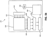
- FIG. 1b is a schematic diagram of components of one embodiment of a radiography detector system.
- the radiography detector system 108 includes an active matrix pixel array 120 having a two-dimensional matrix of pixel elements where electronic charges generated, directly or indirectly, by incident X-rays are sensed and stored.
- gate lines 122 are driven, preferably sequentially, by a row switching control or controller 124 causing all pixels in one row of the active matrix pixel array 120 to output their stored charge onto data lines 126 that are coupled to charge amplifiers 128 at the end of each active matrix pixel array 120 column.
- the charge amplifiers 128 may also perform a multiplexing function in addition to the amplifying function.
- the charge amplifiers 128 send the pixel charge data to analog-to-digital converters (A/D's) 130, where the analog signal is converted to a digital representation. These digital representations are then stored in memory 132 awaiting transmission to the computer 112 at a time determined by the control logic 134. The transmission of the digital representations may be performed by a processor or central processing unit (CPU) 136.
- CPU central processing unit
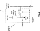
- FIG 2 is a schematic diagram of a pixel level circuit for a pixel within the active matrix pixel array 120 of Figure 1b .
- a two terminal metal-semiconductor-metal (MSM) or metal-insulator-semiconductor-insulator-metal (MISIM) detector 200 that absorbs the incident X-ray photons and generates electronic charge, a two-terminal capacitor 202 to store converted electronic charge and a switch 204, typically a three electrode thin-film-transistor (TFT) switch, for transferring the electronic charge off the pixel.
- a switch 204 typically a three electrode thin-film-transistor (TFT) switch, for transferring the electronic charge off the pixel.
- TFT thin-film-transistor
- One electrode of the MSM detector 200 is connected to a high potential bias terminal 206 that is shared with other pixels in the active matrix pixel array 120 and another of the electrodes is connected to the capacitor 202.
- the capacitor 202 is also connected to a low potential ground terminal 208 which is also shared with other pixels in the active matrix pixel array 120.
- the drain electrode of the TFT 204 is connected to one of the electrodes of the MSM detector 200 and one of the terminals of the capacitor 202.
- the source electrode of the TFT 204 is connected to a pixel data line 210 which is coupled to one of the plurality of data lines 126 described in Figure 1b .
- the gate electrode of the TFT 204 is connected to a pixel gate line 212 which is coupled to one of the plurality of gate lines 122 described in Figure 1b .
- the MSM detector 200 includes a substrate layer 330 such as, but not limited to, glass, steel, aluminium or plastic, with a semiconducting layer 332 deposited atop the substrate layer 330.
- the material for the semiconducting layer 332 is preferably selected from one of amorphous silicon, polysilicon, microcrystalline silicon, epitaxial silicon, amorphous selenium, crystalline selenium, molybdenum sulfide, metal oxide semiconductors, silicon nanowires (for example, to sense infrared wavelengths with high quantum efficiency), or an organic semiconductor, although other materials may be contemplated.
- an optional blocking layer 334 is deposited and then a patterned contact layer yielding at least two electrodes is located atop the optional blocking layer 334. In the absence of the optional blocking layer 334, the contact layer is deposited atop the semiconducting layer 332.
- the at least two electrodes include one sense contact or electrode 336 and one bias contact or electrode 338. It will be understood that the electrodes 336 and 338 may be switched whereby electrode 336 is the bias contact and electrode 338 is the sense electrode. In an alternative embodiment, ohmic or Schottky contacts may be used as the electrodes.
- the layers may be deposited in a pre-determined sequence on top of the substrate layer 330. In this example, the pre-determined sequence is the semiconducting layer 332, the optional blocking layer 334 and then contact layer with the two electrodes 336 and 338. In use, the MSM detector 200 receives and processes top incident light 328 and bottom incident light 329.
- the optional blocking layer 334 can be any one of ohmic, Schottky or insulating layer varieties.
- insulating or wide bandgap semiconductor blocking layers such as, but not limited to, polyimide, polystyrene, PVK, silicon nitride, silicon oxide, silicon oxynitride, Molybdenum Sulfide or transparent metal oxides (such as Indium Gallium Zinc Oxide, Zinc Oxide) can be advantageous in reducing the dark current while maintaining high photocurrent and sensitivity.
- an optional anti-reflective layer may be deposited atop the substrate layer 330 prior to deposition of the semiconducting layer 332.
- the anti-reflective layer is not necessary for operation of the MSM detector 200, in an indirect conversion imaging system, the anti-reflective layer may enhance system performance by increasing the percentage of light photons impinging on the semiconducting layer 332 where photons are absorbed. If an insulating or wide bandgap semiconductor is used as the blocking layer, it can also provide the functionality of an anti-reflective layer.
- FIG 3b a schematic cross-section diagram of a second embodiment of a MSM detector 200 is provided.
- the MSM detector 200 of Figure 3b may be seen as a bottom electrode configuration.
- the deposition of the layers atop the substrate layer 330 may be reversed with respect to the embodiment of Figure 3a .
- an electrode layer patterned to realize a pair of contacts (or electrodes) is deposited on the substrate layer 330. These electrodes may be the sense 336 and bias 338 contacts or electrodes.
- the deposition of the electrodes is followed by the deposition of an optional blocking layer 334 and the semiconducting layer 332.
- an optional anti-reflective layer may be deposited atop the semiconducting layer 332.
- Each of the layers will perform similar functions as disclosed above with respect to Figure 3a .
- the hybrid photoconductive element 400 includes a top electrode MSM detector 410 including sense electrode A 402, bias electrode A 406, optional blocking layer 412 and the semiconducting layer 414 and a bottom electrode MSM detector 416 including sense electrode B 404, bias electrode B 408, optional blocking layer 418 and semiconducting layer 414.
- the top electrode MSM detector 410 is similar to the embodiment shown in Figure 3a and the bottom electrode detector MSM 416 is similar to the embodiment shown in Figure 3b .
- the top 410 and bottom 416 MSM detectors share the common semiconducting layer 414 and a common substrate 420.
- the photoconductive element 400 may be seen as a hybrid MSM (HMSM) structure including a plurality of MSMs.
- HMSM hybrid MSM
- the HMSM or photoconductive element 400 of Figure 4a is able to sense light from opposite sides of the semiconducting layer 414 simultaneously i.e. top incident light 422 is sensed by the top electrode MSM detector 410 and bottom incident light 424 is sensed by the bottom MSM detector 416.
- the blocking layers 412 and 418 When X-ray photons are impinging on the semiconducting layer 414 (thereby causing the resistivity of the semiconducting layer 414 to decrease), the blocking layers 412 and 418, at the higher electric fields, permit, or allow for, a vertical conduction path from the respective bias electrodes 406 and 408 to respective sense contacts 402 and 404 through the respective blocking layers 412 and 418 to the semiconducting layer 414.
- the resistivity of the semiconducting layer 414 is high making the electric field across the blocking layers 412 and 418 lower thus reducing or preventing any injection of current from the bias and/or sense contacts.
- a continuous blocking layer 412 or 418 as opposed to simply patterning the insulating contacts around the bias electrodes 406 or 408 and sense contacts 402 or 404 can lead to a better overall interface with the semiconductor layer 414 with fewer defects and traps as well as encapsulating the semiconducting layer 414 thereby maintaining a higher quantum efficiency.
- a patterning process may degrade the semiconducting layer 414 interface due to its exposure to air and chemicals during the patterning process. However, for certain applications, patterning is necessary and preferred as would be appreciated by one skilled in the art.
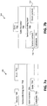
- Figure 4b and 4c show alternate configurations of a hybrid MSM structure, or photoconductive element, where there is a single bias electrode bias electrode 425 placed on the same plane as the sense electrode A 402 ( Figure 4b ) or sense electrode B 404 ( Figure 4c).
- Figure 4d represents another variant of the photoconductive element where the bias electrode A 406 and bias electrode B 408 do not differ in physical placement as compared to the embodiment of Figure 4a , however, they are connected to the same potential unlike the embodiment of Figure 4a where the bias electrodes 406 and 408 may be set at different potentials.
- Figure 4f is a schematic cross-section of yet a further embodiment of a photoconductive element. Similar to the embodiment of Figure 4d , the sense electrodes 402 and 404 are preferably connected to yield a single sense electrode (or two sense electrodes at the same potential) albeit on two sides of the semiconducting layer 414. To yield a single sense electrode, a connection between electrodes on either side of the semiconducting layer can be accomplished by using a via.
- the structure of Figure 4f can enable a higher sensitivity due to better control of the electric field.
- the embodiment of Figure 4f also includes the blocking layers 412 and 418, a semiconducting layer and a substrate 420 along with bias electrodes 406 and 408.
- Figures 4g and 4h are further cross sections of other embodiments of a photoconductive element 400.
- the MSM detectors are stacked on top of each other.
- the process complexity is also increased.
- the element 400 of Figure 4h can help discriminate between different optical wavelengths by sensing the depth of absorption in the semiconducting layers 414 and 434.
- the top semiconducting layer 414 can sense shorter blue and green wavelengths while longer wavelengths like red or near infrared could be absorbed in the bottom semiconducting layer 434.
- the element 400 also includes three bias electrodes 406, 408 and 435 along with a set of a set of optional blocking layers 412, 418, 436 and 438.
- a set of sense 402 and bias 406 electrodes is located atop a blocking layer 412 which along with a pair of other blocking layers 436 and 438 sandwich a pair of semiconducting layers 414 and 434 atop a substrate layer 420.
- HMSM detectors or photoconductive elements of the disclosure can sense light from both sides of the semiconducting layer, these devices can give rise to dual-sided gesture sensitive or touch displays.
- any number of MSM or HMSM detectors can be stacked on top of each other (although the process complexity could increase) as shown in Figures 4g to 4j .
- These types of HMSM stacks can enable either enhanced spectral separation or sensing more than two wavelengths at the same time (for example, infrared and/or color).
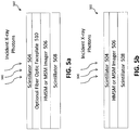
- Detecting optical, or light, photons from both sides of the semiconducting layer 414 can also be used for a higher performance dual energy X-ray imaging system such as schematically shown in Figure 5a .
- a set of X-ray beams 500 containing a spectrum of low, mid and high energies is incident on the X-ray detector 502.
- a top scintillator 504 (absorbing the low energy incident X-ray photons) is placed on top of a digital imager 506 employing either a MSM or HMSM detector (such as disclosed above with respect to Figures 3a to 3c or 4a to 4j ).
- a bottom scintillator 508 is placed behind the imager 506 and absorbs the mid and high energy X-ray photons that are not absorbed in the top scintillator 504.
- Using a HMSM imager 506 enables simultaneous detection of high and low X-ray energies to remove or eliminate motion artifact.
- the HMSM imager 506 is preferably used with a fiber optic faceplate 510 (adapted to serve as a mid-filter) that is placed between the top scintillator 504 and bottom scintillator 508.
- the faceplate 510 can be placed adjacent to the top scintillator 504 (as shown in Figure 5a ) or alternately, between the HMSM imager 506 and the bottom scintillator 508.
- One unique property of the fiber optic faceplate 510 is that it is capable of absorbing some incident X-ray photons 500 but also permits light from the top scintillator 504 to be transmitted to the HMSM imager 506. In other words, the faceplate can improve the detection being performed by the system 502.
- fiber optic faceplates are used with CMOS X-ray imagers where they are designed to reduce the amount of X-ray damage to CMOS X-ray imagers from photons that are not fully absorbed in the overlying scintillator layer.
- the fiber optic faceplate 510 is being used as a mid-filter to filter mid-energy X-rays for dual energy imaging which is different than its use in CMOS X-ray imagers.
- the top scintillator 504 is converting incident X-ray photons into light photons, there is a desire that these light photons reach the top of the HMSM imager 506 for sensing.
- the mid-filter 510 or faceplate assists to filter out the mid-energy X-ray photons to allow for better or improved spectral separation between the lower and higher X-ray energies.
- the top scintillator 504 can be silvered on the top to reduce or minimize light loss through the top and hence enhance light collection within the top electrode of the imager 506.
- the bottom scintillator 508 can be silvered on the bottom to reduce or minimize light loss through the bottom. Light photons generated in the bottom scintillator 508 are to be sensed by the bottom electrodes of the HMSM imager 506.
- an imaging system 502 such as schematically shown in Figure 5b may enable higher, or improved, performance fast-kVp dual energy imaging where the low and high energy X-ray images are detected sequentially by using the top scintillator 504 optimized or directed for low energy X-rays and the combination of top 504 and bottom 508 scintillators optimized or directed for high energy X-rays.
- the high and low energy images are detected by the same X-ray imager so optimization for either high or low energy is challenging.
- the X-ray system includes two distinct imagers to handle both high and low energies.
- the MSM or HMSM imager 506 is shown without a faceplate.
- the spectral separation of a single incident X-ray spectrum would not typically be considered sufficient for a dual energy application, however, by choosing two different thicknesses for the top scintillator 504 and bottom scintillator 508, the imager 506 may be designed to be sensitive to two different X-ray energy spectrums depending on which side the photons are incident upon. In other words, the imaging system may be able to detect X-ray photons simultaneously impinging on both sides of the imager 506.
- an X-ray imager 506 could be optimized for 60 kVp for pediatric imaging on the top side and 120 kVp or typical chest radiography on the opposite side thus serving a dual purpose in the diagnostic room.
- a 50 um pixel pitch imager could be used for high-resolution lower X-ray energy mammography from the top side and the pixels could be binned (e.g. to 100 um x 100 um) for use in higher energy, lower resolution, chest X-ray from the bottom side.
- This type of dual functionality can help reduce the cost of ownership of a digital X-imager or system ray in underserved regions and lower volume clinics and healthcare centers.
- An advantage of the current disclosure is that it enables detection of light from both sides of the substrate or semiconducting layer in a lateral orientation, which exposes the semiconducting layer of the imager or photoconductive element to incident light from both the top and bottom directions without significant impact from contact shadowing.
- transparent electrodes are preferred for the imager 506, however, if this is not feasible, then the staggered MSM in Figure 3c may be used within the imager 506.
- some of the incident X-ray photons are absorbed in the top scintillator 504 while the rest pass through the MSM imager 506 and are absorbed in the bottom scintillator 508 to yield a higher dose efficiency as compared to a traditional X-ray imager with only one scintillator.
- the architecture or system of Figure 5b may also improve the spatial resolution of scintillators without compromising or affecting dose efficiency.
- two half size (e.g. 0.5mm) scintillators can be used, one on the top 504 and the other on the bottom 508.
- Splitting a thick scintillator layer into two thinner layers improves spatial resolution because the X-ray generated optical photon spread is limited to only the half thickness instead of the full. This approach is useful for cost reduction.
- GOS scintillator is well known to be considerably less expensive than structured Csl although its spatial resolution characteristics are poorer thus it is not chosen for high resolution imaging applications.
- using two half thickness GOS scintillators in the architecture shown in Figure 5b may achieve a spatial resolution closer to Csl but at a considerably lower manufacturing cost.
- the architectures shown in Figures 5a and 5b rely on incident X-ray photons 500 that are absorbed in two scintillators that create light photons striking the MSM or HMSM structure 506 from opposite sides.
- the MSM or HMSM imager resides on a substrate layer (e.g. glass, plastic, steel, aluminium etc) as in Figure 3 (substrate layer 330) or Figure 4 (substrate layer 420) and in order to reduce or minimize detrimental blurring effects, the substrate layer is preferably thin (e.g. Corning Willow glass or similar) or purposefully thinned to achieve improved performance.
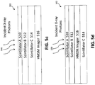
- Figures 5c and Figure 5d are schematic diagrams of multi-spectral (i.e. triple energy) X-ray imaging systems that utilize the HMSM device shown in Figure 4h .
- the system 502 includes three different scintillators 510, 512 and 514 that emit light at three different wavelengths (e.g. blue, green and red).
- the scintillators are placed on top and/or beneath an HMSM imager 516 that can discriminate the light of the three different wavelengths via the properties of the different wavelengths of light absorbed in the semiconductor layers at various depths.
- the three images produced by the three scintillators can be acquired simultaneously implying no motion artifacts. Being able to discriminate between three different X-ray energy spectrums (high, middle and low) can enhance the image quality for X-ray imaging and is akin to X-ray photon counting with three separate energy bins.
- the thickest scintillator 514 is preferably placed below the HMSM imager 516 to reduce light losses and scattering for scintillator A 510 and scintillator B 512 and also to improve spatial resolution for scintillator C 514 as explained earlier.
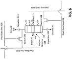
- Figure 6 is directed at a pixel level circuit diagram including a HMSM detector 618.
- the HMSM detector 618 is the one shown in Figure 4a which includes a top electrode detector 617 and a bottom electrode detector 619.
- the HMSM detector may be any of the ones previously discussed.
- the top HMSM detector 617 preferably has one electrode (bias electrode A 406) connected to a bias 620 and the other electrode (sense electrode A 402) connected to the switch 622 and a storage capacitor 624.
- the second terminal of the capacitor 624 is connected to ground 626.
- the TFT switch 622 is driven by the gate line 628 and the top HMSM detector output is transferred to a pixel data line 630 when the switch 622 is ON.
- the bottom electrode detector has one electrode (bias electrode B 408) connected to a bias 632 and the other electrode (sense electrode B 404) is connected to the switch 634 and a storage capacitor 636.
- the second terminal of the capacitor 636 is connected to ground 626.
- the TFT switch 634 is driven by the gate line 638 and the bottom output is transferred to a pixel data line 640.
- the embodiment or implementation shown in Figure 6 is very general as there is no multiplexing of common signals.
- FIG. 7a is a schematic diagram of one embodiment of a TFT structure.
- the TFT structure 700 may be seen as a bottom gate, inverted staggered TFT structure.
- the TFT structure 700 includes a substrate 702 (e.g. glass or plastic) having a patterned gate electrode 704, followed by a gate insulator 706, a semiconducting layer 708 and a patterned contact layer defining the source 710 and drain 712 contacts.
- FIG. 7b is a schematic diagram of another embodiment of a TFT structure.
- This embodiment may be seen as a top gate, inverted staggered TFT structure 700 with the layers in a reverse configuration compared to the embodiment of Figure 7a .
- Both are implementations of amorphous silicon TFTs in use by the display industry today. Similar cross-sections can be drawn for IGZO, organic, polysilicon and nanowire TFTs and other large area electronics materials as understood by one skilled in the art.
- FIG 8 shows a pixel level circuit diagram including a HMSM detector 400, such as the one shown in Figure 4d .
- HMSM detector 400 such as the one shown in Figure 4d .
- This implementation may be used in system which requires or benefits from the multiplexing of many common signals.
- a top electrode MSM detector 410 and a bottom electrode MSM detector 416 such as discussed with respect to Figure 4d above.
- the top and bottom electrodes detectors each have one electrode (bias electrodes 406 and 408, respectively) connected to a common bias 800.
- the other electrode for the top HMSM detector (such as sense electrode A 402) is connected to the switch 802 and a storage capacitor 804.
- the second terminal of the capacitor 804 is connected to common ground 806.
- the TFT switch 802 is driven by the gate line 808 and the sense electrode A 402 output is transferred to a pixel data line 810 when the switch 802 is ON.
- the bottom sense electrode (such as sense electrode B 404) is connected to the switch 812 and a storage capacitor 814.
- the second terminal of the capacitor 814 is connected to a common ground 806.
- the TFT switch 812 is driven by the common gate line 808 to ensure simultaneous data capture while the bottom sense electrode B 404 output is transferred to a discrete pixel data line 816.
- Figure 9 shows a cross-section of a preferred implementation of a pixel using the HMSM of Figure 4d , the bottom gate TFT architecture of Figure 7a and the pixel circuit of Figure 8 .
- the structure 900 further includes an amorphous silicon nitride anti-reflective layer 912 and an amorphous silicon nitride passivation layer 914.
- Two capacitor cross-sections are shown, one 916 for the bottom (sense A electrode or electrodes 903) and the other 918 for the top sense electrode (sense B electrode of electrodes 904).
- the capacitor cross-sections shows the bottom plate shared with either the sense A electrode 903 or sense B electrode 904 along with a top capacitor plate connected to ground 920, typically a low electric potential.
- the capacitor dielectric in this case is within the amorphous silicon nitride layer 912, and is shared with the anti-reflective layer in the HMSM detector cross-section 900.
- the first TFT A cross-section 922 includes sense A electrode 903 functioning as a TFT source/drain electrode with the other TFT source/drain electrode being connected to the pixel data line 924 (i.e. the data line 812 in Figure 8 ). Also shown is a gate electrode 926 connected to the pixel gate line such as pixel gate line 808 of Figure 8 .
- the second TFT B cross-section 928 includes a sense B electrode 904 functioning as a TFT source/drain electrode with the other TFT source/drain electrode being connected to the pixel data line 930 (i.e. the data line 168 in Figure 8 ) .
- an amorphous silicon layer 932 is the active layer and this may or may not be shared with the HMSM detector cross-section 900. In Figure 9 , it is not shared since a thicker semiconducting layer could be necessary for the HMSM structure 900.
- the TFT gate dielectric is formed by an amorphous silicon nitride layer 912, shared with the anti-reflective layer shown in the HMSM detector's cross-section 900 and also the dielectric layer for both capacitor A 916 and capacitor B 918.
- the TFT gate dielectric can serve as an anti-reflective coating layer.
- the HMSM detector such as detector 400 of Figure 8
- the horizontal interface is primarily important.
- Using an insulator layer helps protect the interface to the semiconducting layer.
- device performance remains stable in the long term even if the HMSM detector 400 is built in a standard TFT manufacturing process.
- the MSM or HMSM does not necessarily need a p+ doped layer like the PIN photodiode, blue light emitting phosphors can work which can help reduce the required thickness of the amorphous silicon layer 910 thus enabling sharing with the TFT amorphous silicon layer 932.
- the HMSM detector may use any one of a number of insulating layers between the contact electrodes and the amorphous silicon, i.e. polyimide, polystyrene, amorphous silicon nitride, amorphous silicon oxide or amorphous silicon oxynitride.
- the anti-reflective layer can be a layer of the same set as described above.
- the HMSM detector 400 is connected to two capacitors 1000, 1002 that store the signal created by incident photons on the bottom 1004 and 1006 of the HMSM detector 400. Both capacitors have at least one electrode connected to a common ground 1008 with the other being connected to switches 1010, 1012 that are controlled by discrete pixel gate lines 1014, 1016. The switches transfer the signal to the input of a dual or single stage pixel amplifier 1018, such as disclosed in US Patent Publication No. 20040135911 to Karim et al.
Landscapes
- Health & Medical Sciences (AREA)
- Life Sciences & Earth Sciences (AREA)
- Physics & Mathematics (AREA)
- Molecular Biology (AREA)
- High Energy & Nuclear Physics (AREA)
- General Physics & Mathematics (AREA)
- Spectroscopy & Molecular Physics (AREA)
- Engineering & Computer Science (AREA)
- Medical Informatics (AREA)
- Optics & Photonics (AREA)
- Nuclear Medicine, Radiotherapy & Molecular Imaging (AREA)
- Biomedical Technology (AREA)
- General Health & Medical Sciences (AREA)
- Radiology & Medical Imaging (AREA)
- Surgery (AREA)
- Animal Behavior & Ethology (AREA)
- Heart & Thoracic Surgery (AREA)
- Public Health (AREA)
- Veterinary Medicine (AREA)
- Pathology (AREA)
- Biophysics (AREA)
- Solid State Image Pick-Up Elements (AREA)
- Measurement Of Radiation (AREA)
Description
- The disclosure relates generally to digital imaging systems, and more particularly, to a multi-sensor pixel architecture for use in a digital imaging system, and still more particularly to a detector element according to the preamble of claim 1.
- Traditionally, X-ray diagnostic processes record x-ray image patterns on silver halide films. These systems typically direct an initially uniform pattern of impinging X-ray radiation, or X-rays, through an object to be studied, intercept the modulated pattern of X-ray radiation after the X-rays pass through the object to be studied with an X-ray radiation intensifying screen, record the modified pattern on a silver halide film, and chemically transform the latent pattern into a permanent and visible image called a radiograph.
- Radiographs are produced by using layers of radiation sensitive materials to directly capture radiographic images as modulated patterns of electrical charges. Depending on the intensity of the incident X-ray radiation, electrical charges generated, either electrically or optically (indirectly via a scintillator) from the X-ray radiation, are quantized using a regularly arranged array of discrete solid-state radiation sensors.
- Recently, there has been rapid development in the area of large area, flat-panel, digital X-ray imagers for digital radiology using active matrix technologies. An active matrix includes a two-dimensional array (of which, each element is called a pixel) of thin-film-transistors (TFTs) made with a large area compatible semiconductor material.
- There are two general approaches to manufacturing flat-panel X-ray imagers. These approaches can be seen as a direct approach or an indirect approach. The direct approach primarily uses an amorphous selenium photoconductor as the X-ray to electric charge converting layer coupled directly to the active matrix. In the indirect approach, a phosphor screen or scintillator (e.g. Csl, GdOS etc) is used to convert X-rays to light photons which are then converted to electric charge using an additional pixel level light sensor fabricated with the TFT on the active matrix array.
- Although the concept of large area dual energy X-ray imaging by stacking two X-ray imagers on top of each other has been around even in the era of computed radiography, the difficulty in acquiring a good quality image, increase in the overall time of the procedure and also the diagnostic time associated with two images, has limited its use in mainstream medicine. Stacking two imagers also drives the cost of production up linearly. More recently, with the rise of digital X-ray imagers, a technique called fast kVp switching has gained some acceptance where the X-ray source is switched within typically < 100 ms between the high and low X-ray exposures while using a single digital imager to acquire the images in sequence. While a dual energy image can be obtained using this approach, this technique is susceptible to motion artifacts for example, due to patient breathing. Also, the digital imager can only be optimized to capture either the low or high-energy spectrum but this leads to a tradeoff between resolution and dose efficiency.
- Commercially available flat-panel imagers are optimized to sense a single spectrum of incident X-ray energies e.g. a chest radiography imager is optimized to sense a 100 kVp spectrum or alternately, a mammography imager is designed to sense a 30 kVp spectrum. The optimization is undertaken usually by selecting an optimum thickness of the photoconductor for direct imaging or alternately, an optimum thickness of a scintillator for indirect imaging. If the scintillator is too thin, absorption efficiency suffers and if the scintillator is too thick, blurring increases.
-
US2015263061 A1 discloses a detector element for use in a digital imaging system, the detector element comprising: at least one semiconducting layer for absorbing radiation incident on opposite sides of the at least one semiconducting layer; characterized by a set of electrodes located on one side of the at least one semiconducting layer for transmitting a signal associated with the radiation absorbed by the at least one semiconducting layer; wherein the signal is transmitted to a set of readout electronics. The presentation "Low cost digital detector technology for emerging economies" by Karim S Karim of the University of Waterloo, shows an amorphous silicon MSM sensor integrated with an amplified pixel which is illuminated from both side. The drawing of the MSM sensor clearly shows an Amorphous silicon semiconducting layer with two metal electrodes on top of it. Accordingly, there is a need for an improved digital X-ray imager. - The present disclosure is directed at a system and method for a multi-sensor pixel architecture. The pixel architecture is integrated in a photoconductive sensing element within a single pixel. In one aspect, this enables the creation of a next generation dual energy imager. Among its advantages, the system of the disclosure may acquire dual energy images simultaneously, may be optimized independently of each other and/or may reduce or minimize manufacturing cost. These and other advantages of the aspects of the present disclosure will be understood in conjunction with the following detailed description and accompanying drawings.
- An imager capable of sensing two different energy spectrums, however, can be helpful in distinguishing between two materials of different density e.g. bone and soft tissue. Such a technique has been employed in dual energy x-ray absorptiometry (i.e. bone scans) where linear scanners are used to acquire the dual energy images. Dual energy is gaining prominence in computed tomography (CT) also where crystalline or polycrystalline detectors are interfaced to photon counting circuits that are capable of distinguishing between incident X-ray energy via two or more distinct thresholds built into the pixel circuit. However, to date, dual energy large area X-ray imagers have not gained significant traction.
- The imager of the disclosure is capable of, at least one of, acquiring dual energy images simultaneously without motion artifact, is optimized for spatial resolution and dose efficiency when acquiring both high and low energy X-ray spectrums, and does not drive up the cost of production like a conventional imager stacking approach.
- In one aspect of the disclosure, there is provided a detector element for use in a digital imaging system, the detector element including at least one semiconducting layer for absorbing radiation incident on opposite sides of the at least one semiconducting layer; and a set of electrodes located on one side of the at least one semiconducting layer for transmitting a signal associated with the radiation absorbed by the at least one semiconducting layer. The signal is then transmitted to a set of readout electronics. In another aspect, the set of electrodes includes a sense electrode and a bias electrode. In yet a further aspect, the sense electrode and the bias electrode are spaced apart laterally. The detector element may also include a blocking layer situated between the set of electrodes and said semiconducting layer.
- According to the invention, there is provided a detector element for a digital imaging system, the detector element including at least one top electrode metal-semiconductor-metal (MSM) detector; and at least one bottom electrode MSM detector; wherein said at least one top electrode MSM detector and said at least one bottom electrode MSM detector share a common semiconducting layer.
- Embodiments of the disclosure will now be described, by way of example only, with reference to the attached drawings, in which:
-
Figure 1a illustrates a schematic diagram of a system for radiographic imaging; -
Figure 1b is a schematic diagram of a radiography detector system; -
Figure 2 is a two-dimensional active matrix imaging array structure; -
Figures 3a to 3c are schematic diagrams of MSM detectors; -
Figures 4a to 4j are schematic diagrams of hybrid MSM according to the claimed invention; -
Figures 5a to 5d are schematic diagrams of dual X-ray imaging systems; -
Figure 6 is a schematic diagram of a pixel level circuit diagram; -
Figures 7a and 7b are schematic diagrams of thin-film-transistor (TFT) structures; -
Figure 8 is another schematic diagram of a pixel level circuit diagram; -
Figure 9 is a cross-section of a pixel element; and -
Figure 10 is a schematic diagram of a further embodiment of a pixel level circuit diagram. - The following description is presented to enable one of ordinary skill in the art to make and use the disclosure and is provided in the context of a patent application and its requirements. Various modifications to the embodiments will be readily apparent to those skilled in the art and the generic principles herein may be applied to other embodiments.
- The present disclosure relates to a pixel architecture, preferably for use in a digital imaging system, which includes a multi-sensor metal-semiconductor-metal (MSM) detector integrated with a switching, or photoconductive, element for a digital imaging system. In a preferred type of application, the digital imaging system is a radiography imaging system.
- Examples of metal-semiconductor-metal (MSM) detectors are described in the following publications: (1) S. Ghanbarzadeh, S. Abbaszadeh and K.S. Karim, " Low dark current amorphous silicon Metal-Semiconductor-Metal photodetector for digital imaging applications", IEEE Electron Device Letters (2014) and (2)
US 9,269,838 B2 -
Figure 1a illustrates a schematic diagram of a radiographic imaging environment, or system. Thesystem 100 includes anX-ray radiation source 102 that generates X-ray radiation, in the form of a set ofX-ray beams 104, that is transmitted towards an object ofinterest 106 such as a patient's hand, for imaging by aradiography detector system 108. In the present disclosure, theradiography detector system 108 preferably includes a large area, flat-panel detector based on active matrix technologies to achieve, or produce an image of theobject 106. In general, theobject 106 to be imaged is positioned between theX-ray radiation source 102 and theradiography detector system 108. X-rays, which pass through theobject 106, interact with theradiography detector system 108. - In direct imaging, the X-rays generate electronic charge within the
radiography detector system 108 such that there is no need for ascintillator 110. In indirect imaging, the X-rays generate light photons as they pass through a phosphor screen orscintillator 110 within theradiography detector system 108. Different materials are contemplated for the scintillator including, but not limited to, Caesium Iodide (Csl), Gadolinium oxysulfide (GOS) or Calcium Tungsten Oxide (CaWO4). These indirectly generated light photons then further generate electronic charge within theradiography detector system 108. - The image 115 that is produced by the
radiography detector system 108 can then be viewed on adisplay 117 of acomputer 112 or computing system. For someradiography detector systems 108,synchronization hardware 114 may be necessary to obtain the correct timing between theX-ray source 102 and theradiography detector system 108 that is sampling the impinging set of X-ray beams 104. -
Figure 1b is a schematic diagram of components of one embodiment of a radiography detector system. In the current example, theradiography detector system 108 includes an activematrix pixel array 120 having a two-dimensional matrix of pixel elements where electronic charges generated, directly or indirectly, by incident X-rays are sensed and stored. To access the stored charge at each pixel,gate lines 122 are driven, preferably sequentially, by a row switching control orcontroller 124 causing all pixels in one row of the activematrix pixel array 120 to output their stored charge ontodata lines 126 that are coupled to chargeamplifiers 128 at the end of each activematrix pixel array 120 column. Thecharge amplifiers 128 may also perform a multiplexing function in addition to the amplifying function. Thecharge amplifiers 128 send the pixel charge data to analog-to-digital converters (A/D's) 130, where the analog signal is converted to a digital representation. These digital representations are then stored inmemory 132 awaiting transmission to thecomputer 112 at a time determined by thecontrol logic 134. The transmission of the digital representations may be performed by a processor or central processing unit (CPU) 136. -
Figure 2 is a schematic diagram of a pixel level circuit for a pixel within the activematrix pixel array 120 ofFigure 1b . Within eachpixel 201 is a two terminal metal-semiconductor-metal (MSM) or metal-insulator-semiconductor-insulator-metal (MISIM)detector 200 that absorbs the incident X-ray photons and generates electronic charge, a two-terminal capacitor 202 to store converted electronic charge and aswitch 204, typically a three electrode thin-film-transistor (TFT) switch, for transferring the electronic charge off the pixel. It will be understood that thecapacitor 202 is an optional component within thispixel 201. For clarity sake, when the description refers to a MSM detector, a MISIM detector may also be contemplated. - One electrode of the
MSM detector 200 is connected to a highpotential bias terminal 206 that is shared with other pixels in the activematrix pixel array 120 and another of the electrodes is connected to thecapacitor 202. Thecapacitor 202 is also connected to a lowpotential ground terminal 208 which is also shared with other pixels in the activematrix pixel array 120. The drain electrode of theTFT 204 is connected to one of the electrodes of theMSM detector 200 and one of the terminals of thecapacitor 202. The source electrode of theTFT 204 is connected to a pixel data line 210 which is coupled to one of the plurality ofdata lines 126 described inFigure 1b . The gate electrode of theTFT 204 is connected to apixel gate line 212 which is coupled to one of the plurality ofgate lines 122 described inFigure 1b . - Turning to
Figure 3a , a schematic cross-section diagram of a first embodiment of theMSM detector 200 is shown. In this embodiment, theMSM detector 200 may be seen as being in a top electrode configuration. TheMSM detector 200 includes asubstrate layer 330 such as, but not limited to, glass, steel, aluminium or plastic, with asemiconducting layer 332 deposited atop thesubstrate layer 330. The material for thesemiconducting layer 332 is preferably selected from one of amorphous silicon, polysilicon, microcrystalline silicon, epitaxial silicon, amorphous selenium, crystalline selenium, molybdenum sulfide, metal oxide semiconductors, silicon nanowires (for example, to sense infrared wavelengths with high quantum efficiency), or an organic semiconductor, although other materials may be contemplated. Atop thesemiconducting layer 332, anoptional blocking layer 334 is deposited and then a patterned contact layer yielding at least two electrodes is located atop theoptional blocking layer 334. In the absence of theoptional blocking layer 334, the contact layer is deposited atop thesemiconducting layer 332. In the current example, the at least two electrodes include one sense contact orelectrode 336 and one bias contact orelectrode 338. It will be understood that theelectrodes electrode 336 is the bias contact andelectrode 338 is the sense electrode. In an alternative embodiment, ohmic or Schottky contacts may be used as the electrodes. In a preferred embodiment, the layers may be deposited in a pre-determined sequence on top of thesubstrate layer 330. In this example, the pre-determined sequence is thesemiconducting layer 332, theoptional blocking layer 334 and then contact layer with the twoelectrodes MSM detector 200 receives and processestop incident light 328 andbottom incident light 329. - The
optional blocking layer 334 can be any one of ohmic, Schottky or insulating layer varieties. In particular, insulating or wide bandgap semiconductor blocking layers such as, but not limited to, polyimide, polystyrene, PVK, silicon nitride, silicon oxide, silicon oxynitride, Molybdenum Sulfide or transparent metal oxides (such as Indium Gallium Zinc Oxide, Zinc Oxide) can be advantageous in reducing the dark current while maintaining high photocurrent and sensitivity. Although not shown, an optional anti-reflective layer may be deposited atop thesubstrate layer 330 prior to deposition of thesemiconducting layer 332. While the anti-reflective layer is not necessary for operation of theMSM detector 200, in an indirect conversion imaging system, the anti-reflective layer may enhance system performance by increasing the percentage of light photons impinging on thesemiconducting layer 332 where photons are absorbed. If an insulating or wide bandgap semiconductor is used as the blocking layer, it can also provide the functionality of an anti-reflective layer. - In
Figure 3b , a schematic cross-section diagram of a second embodiment of aMSM detector 200 is provided. TheMSM detector 200 ofFigure 3b may be seen as a bottom electrode configuration. In the current embodiment, the deposition of the layers atop thesubstrate layer 330 may be reversed with respect to the embodiment ofFigure 3a . Firstly, an electrode layer patterned to realize a pair of contacts (or electrodes) is deposited on thesubstrate layer 330. These electrodes may be thesense 336 andbias 338 contacts or electrodes. The deposition of the electrodes is followed by the deposition of anoptional blocking layer 334 and thesemiconducting layer 332. Although not shown, an optional anti-reflective layer may be deposited atop thesemiconducting layer 332. Each of the layers will perform similar functions as disclosed above with respect toFigure 3a . - Turning to
Figure 3c , a schematic cross-section diagram of another example of aMSM detector 200 is shown. The arrangement ofFigure 3c may be seen as a staggered electrode arrangement. In this example, thesense 336 andbias 338 contacts are placed on opposite sides of thesemiconducting layer 332 but spaced apart laterally. AlthoughFigure 3c shows thesense electrode 336 in a position above thebias electrode 338, it will be understood that this may be reversed with thebias electrode 338 in a position above thesense electrode 336. TheMSM detector 200 further includes a pair of optional blocking layers 334 on either side of thesemiconducting layer 332. With thebias electrode 338, theoptional blocking layer 334b encapsulates thebias electrode 338 while with thesense electrode 336, theelectrode 336 is atop the otheroptional blocking layer 334a. - In
Figure 4a , a schematic diagram of a cross-section of a first implementation of a hybrid MSM (HMSM) photoconductive element is shown. In the current embodiment, thephotoconductive element 400 includes at least four electrodes seen assense electrode A 402, asense electrode B 404, abias electrode A 406 and abias electrode B 408. In an alternative embodiment, further electrodes may be included and arranged in a comb configuration as would be understood by one skilled in the art. - The hybrid
photoconductive element 400 includes a topelectrode MSM detector 410 includingsense electrode A 402,bias electrode A 406,optional blocking layer 412 and thesemiconducting layer 414 and a bottomelectrode MSM detector 416 includingsense electrode B 404,bias electrode B 408,optional blocking layer 418 andsemiconducting layer 414. The topelectrode MSM detector 410 is similar to the embodiment shown inFigure 3a and the bottomelectrode detector MSM 416 is similar to the embodiment shown inFigure 3b . - As can be seen, the top 410 and bottom 416 MSM detectors share the
common semiconducting layer 414 and acommon substrate 420. Due to the combination of the two types of electrode MSM detectors, thephotoconductive element 400 may be seen as a hybrid MSM (HMSM) structure including a plurality of MSMs. The HMSM orphotoconductive element 400 ofFigure 4a is able to sense light from opposite sides of thesemiconducting layer 414 simultaneously i.e.top incident light 422 is sensed by the topelectrode MSM detector 410 andbottom incident light 424 is sensed by thebottom MSM detector 416. - Generally, dark current is an issue with MSM detectors that do not employ blocking layers or at the very least, some kind of treatment of the electrodes, such as silicidation. Dark current is known to reduce the dynamic range, (or alternately, the range of input signal amplitudes the detector is sensitive to) of the detector and the resultant quality of the image being produced. Dark current is a function of the electric field applied on the bias contacts, or
electrodes semiconducting layer 414. If photocurrent is maintained at a high level while dark current is reduced or if a higher electric potential is applied to thebias contacts - In experiments, the current design when the
top MSM detector 410 includes an insulating or wide bandgapsemiconductor blocking layer 412 and thebottom MSM detector 416 includes an insulating or wide bandgapsemiconductor blocking layer 418, certain advantages were achieved or recognized. These benefits included, but are not limited to, reduced dark currents when there are no X-ray photons impinging on thesemiconducting layer 414 and high photocurrent enabled when X-ray photons impinged on thesemiconducting layer 414. - In one embodiment, in order to achieve, or recognize, these two advantages, the characteristics of the blocking layers 412 and 418 were carefully determined (both material type and thickness) to provide a low defect density interface with the
semiconducting layer 414 and to have a dielectric strength for device operation at high fields. Furthermore, thesemiconducting layer 414 thickness and theblocking layer semiconducting layer 414 thickness), applied electric bias and material properties. - When X-ray photons are impinging on the semiconducting layer 414 (thereby causing the resistivity of the
semiconducting layer 414 to decrease), the blockinglayers respective bias electrodes respective sense contacts semiconducting layer 414. In the dark, the resistivity of thesemiconducting layer 414 is high making the electric field across the blockinglayers - In a preferred embodiment, the characteristics of the blocking layers 412 and 418 are selected such that they can also overcome the response time challenge while still maintaining a low dark current by limiting
bias sense blocking layer incompatible blocking layer semiconducting layer 414 so that traps and defects may cause a drop in the HMSM quantum efficiency. - For example, during experiments, it was determined that using an amorphous
silicon semiconducting layer 414 of a thickness of at least 4000 nm works well with 100-300 nmpolyimide blocking layers 412 and/or 418 and yields a good quality, or improved, interface with high external quantum efficiency (above 65%). If thesemiconducting layer 414 is changed from amorphous silicon to a metal oxide, such as indium gallium zinc oxide (IGZO) or even polysilicon, both of which have different material properties and absorption coefficients, different characteristics for the blocking layers (for interface purposes), thickness and maximum bias voltage applied are necessary, or preferred. - Moreover, a
continuous blocking layer bias electrodes sense contacts semiconductor layer 414 with fewer defects and traps as well as encapsulating thesemiconducting layer 414 thereby maintaining a higher quantum efficiency. A patterning process may degrade thesemiconducting layer 414 interface due to its exposure to air and chemicals during the patterning process. However, for certain applications, patterning is necessary and preferred as would be appreciated by one skilled in the art. - Furthermore, if the
bias electrodes sense electrodes layers semiconducting layer 414 through transparent contacts or electrodes. Alternately, discrete anti-reflective (AR)coatings Figure 4e . -
Figure 4b and4c show alternate configurations of a hybrid MSM structure, or photoconductive element, where there is a single biaselectrode bias electrode 425 placed on the same plane as the sense electrode A 402 (Figure 4b ) or sense electrode B 404 (Figure 4c). Figure 4d represents another variant of the photoconductive element where thebias electrode A 406 andbias electrode B 408 do not differ in physical placement as compared to the embodiment ofFigure 4a , however, they are connected to the same potential unlike the embodiment ofFigure 4a where thebias electrodes -
Figure 4f is a schematic cross-section of yet a further embodiment of a photoconductive element. Similar to the embodiment ofFigure 4d , thesense electrodes semiconducting layer 414. To yield a single sense electrode, a connection between electrodes on either side of the semiconducting layer can be accomplished by using a via. The structure ofFigure 4f can enable a higher sensitivity due to better control of the electric field. The embodiment ofFigure 4f also includes the blocking layers 412 and 418, a semiconducting layer and asubstrate 420 along withbias electrodes -
Figures 4g and 4h are further cross sections of other embodiments of aphotoconductive element 400. In these embodiments, the MSM detectors are stacked on top of each other. In these embodiments, the process complexity is also increased. - In
Figure 4g , thephotoconductive element 400 includes a set ofsense electrodes bias electrodes substrate layer 420 is anoptional blocking layer 438 on which asemiconducting layer 434 is deposited. A further pair of optional blocking layers 436 and 418 is then deposited atop thesemiconducting layer 434 with one of the blocking layers 418 encapsulating thesense electrode 402 andbias electrode 406. Afurther semiconducting layer 414 is deposited atop theoptional blocking layer 418. Finally, in the current embodiment, ananti-reflective layer 440 is deposited atop thesemiconducting layer 412. - In
Figure 4h , there are threesense electrodes photoconductive element 400. For example, for top incident light 422 impinging from the top of theelement 400, theelement 400 ofFigure 4h can help discriminate between different optical wavelengths by sensing the depth of absorption in thesemiconducting layers semiconducting layer 414 can sense shorter blue and green wavelengths while longer wavelengths like red or near infrared could be absorbed in thebottom semiconducting layer 434. This type of discrimination is one factor for accurate biometric fingerprint or hand scanning where a multi-spectral sensor can help distinguish between a live finger and a model by making use of red light that penetrates the human skin or even for multi-energy X-ray imaging as will be described later on. Theelement 400 also includes threebias electrodes - Turning to
Figure 4i , thephotoconductive element 400 includes ananti-reflective layer 440 atop a firstsemiconducting layer 414. Anoptional blocking layer 418, on the other side of the firstsemiconducting layer 414, encapsulates thesense 402 andbias 406 electrodes. An insulatinglayer 442, encapsulating thesense 404 andbias 408 electrodes, is located between theoptional blocking layer 418 and anotherblocking layer 438. Between theblocking layer 438 and thesubstrate layer 420 is a secondsemiconducting layer 434. - In the embodiment of
Figure 4j , a set ofsense 402 andbias 406 electrodes is located atop ablocking layer 412 which along with a pair of other blockinglayers semiconducting layers substrate layer 420. - In each of the HMSM structures shown in
Figure 4 , different applications may be appreciated. For example, in the consumer display field, as the HMSM detectors or photoconductive elements of the disclosure can sense light from both sides of the semiconducting layer, these devices can give rise to dual-sided gesture sensitive or touch displays. In manufacture, any number of MSM or HMSM detectors can be stacked on top of each other (although the process complexity could increase) as shown inFigures 4g to 4j . These types of HMSM stacks can enable either enhanced spectral separation or sensing more than two wavelengths at the same time (for example, infrared and/or color). - Detecting optical, or light, photons from both sides of the
semiconducting layer 414 can also be used for a higher performance dual energy X-ray imaging system such as schematically shown inFigure 5a . In this embodiment, a set ofX-ray beams 500 containing a spectrum of low, mid and high energies is incident on theX-ray detector 502. A top scintillator 504 (absorbing the low energy incident X-ray photons) is placed on top of a digital imager 506 employing either a MSM or HMSM detector (such as disclosed above with respect toFigures 3a to 3c or4a to 4j ). Abottom scintillator 508 is placed behind the imager 506 and absorbs the mid and high energy X-ray photons that are not absorbed in thetop scintillator 504. Using a HMSM imager 506 enables simultaneous detection of high and low X-ray energies to remove or eliminate motion artifact. - For the application of dual energy X-ray imaging, the HMSM imager 506 is preferably used with a fiber optic faceplate 510 (adapted to serve as a mid-filter) that is placed between the
top scintillator 504 andbottom scintillator 508. Thefaceplate 510 can be placed adjacent to the top scintillator 504 (as shown inFigure 5a ) or alternately, between the HMSM imager 506 and thebottom scintillator 508. One unique property of thefiber optic faceplate 510 is that it is capable of absorbing someincident X-ray photons 500 but also permits light from thetop scintillator 504 to be transmitted to the HMSM imager 506. In other words, the faceplate can improve the detection being performed by thesystem 502. - In some circumstances, fiber optic faceplates are used with CMOS X-ray imagers where they are designed to reduce the amount of X-ray damage to CMOS X-ray imagers from photons that are not fully absorbed in the overlying scintillator layer. In the current disclosure, the
fiber optic faceplate 510 is being used as a mid-filter to filter mid-energy X-rays for dual energy imaging which is different than its use in CMOS X-ray imagers. - Since the
top scintillator 504 is converting incident X-ray photons into light photons, there is a desire that these light photons reach the top of the HMSM imager 506 for sensing. The mid-filter 510 or faceplate assists to filter out the mid-energy X-ray photons to allow for better or improved spectral separation between the lower and higher X-ray energies. In one embodiment, thetop scintillator 504 can be silvered on the top to reduce or minimize light loss through the top and hence enhance light collection within the top electrode of the imager 506. Similarly, thebottom scintillator 508 can be silvered on the bottom to reduce or minimize light loss through the bottom. Light photons generated in thebottom scintillator 508 are to be sensed by the bottom electrodes of the HMSM imager 506. - Using an
imaging system 502 such as schematically shown inFigure 5b may enable higher, or improved, performance fast-kVp dual energy imaging where the low and high energy X-ray images are detected sequentially by using thetop scintillator 504 optimized or directed for low energy X-rays and the combination of top 504 and bottom 508 scintillators optimized or directed for high energy X-rays. In the traditional fast-kVp switching approach, the high and low energy images are detected by the same X-ray imager so optimization for either high or low energy is challenging. In the current system, the X-ray system includes two distinct imagers to handle both high and low energies. - Even in a traditional single X-ray energy spectrum application, use of a pair of scintillators on opposite side of the MSM or HMSM imager 506 can increase functionality, higher dose efficiency, higher spatial resolution or lower cost. For example, in
Figure 5b , the MSM or HMSM imager 506 is shown without a faceplate. In this embodiment, the spectral separation of a single incident X-ray spectrum would not typically be considered sufficient for a dual energy application, however, by choosing two different thicknesses for thetop scintillator 504 andbottom scintillator 508, the imager 506 may be designed to be sensitive to two different X-ray energy spectrums depending on which side the photons are incident upon. In other words, the imaging system may be able to detect X-ray photons simultaneously impinging on both sides of the imager 506. - For example, an X-ray imager 506 could be optimized for 60 kVp for pediatric imaging on the top side and 120 kVp or typical chest radiography on the opposite side thus serving a dual purpose in the diagnostic room. Alternately, a 50 um pixel pitch imager could be used for high-resolution lower X-ray energy mammography from the top side and the pixels could be binned (e.g. to 100 um x 100 um) for use in higher energy, lower resolution, chest X-ray from the bottom side. This type of dual functionality can help reduce the cost of ownership of a digital X-imager or system ray in underserved regions and lower volume clinics and healthcare centers.
- An advantage of the current disclosure is that it enables detection of light from both sides of the substrate or semiconducting layer in a lateral orientation, which exposes the semiconducting layer of the imager or photoconductive element to incident light from both the top and bottom directions without significant impact from contact shadowing. To increase or maximize the light being sensed from both sides, transparent electrodes are preferred for the imager 506, however, if this is not feasible, then the staggered MSM in
Figure 3c may be used within the imager 506. - Higher energy X-rays generally require thicker scintillators to absorb all incident photons, however, thicker scintillators do not provide the best spatial resolution due to light scattering. The spatial resolution and dose efficiency tradeoff is especially pronounced in traditional scintillators like gadolinium oxysulphide (GOS:Tb) and to some extent, for structured Csl:TI as well. For structured Csl:TI scintillators, the deposition processes and equipment are typically not designed to exceed 1mm deposition thicknesses limiting the dose efficiency for X-ray energies of 160 keV or higher e.g. in non-destructive test applications. The architecture shown in
Figure 5b can also be used to increase dose efficiency. In one implementation for high X-ray energy imaging, some of the incident X-ray photons are absorbed in thetop scintillator 504 while the rest pass through the MSM imager 506 and are absorbed in thebottom scintillator 508 to yield a higher dose efficiency as compared to a traditional X-ray imager with only one scintillator. - The architecture or system of
Figure 5b may also improve the spatial resolution of scintillators without compromising or affecting dose efficiency. For example, instead of a single thick (e.g. 1mm) scintillator to detect X-rays photon incident on the top, two half size (e.g. 0.5mm) scintillators can be used, one on the top 504 and the other on the bottom 508. Splitting a thick scintillator layer into two thinner layers improves spatial resolution because the X-ray generated optical photon spread is limited to only the half thickness instead of the full. This approach is useful for cost reduction. For example, GOS scintillator is well known to be considerably less expensive than structured Csl although its spatial resolution characteristics are poorer thus it is not chosen for high resolution imaging applications. However, using two half thickness GOS scintillators in the architecture shown inFigure 5b may achieve a spatial resolution closer to Csl but at a considerably lower manufacturing cost. - Lastly, the architectures shown in
Figures 5a and 5b rely onincident X-ray photons 500 that are absorbed in two scintillators that create light photons striking the MSM or HMSM structure 506 from opposite sides. It would be understood to one skilled in the art that the MSM or HMSM imager resides on a substrate layer (e.g. glass, plastic, steel, aluminium etc) as inFigure 3 (substrate layer 330) orFigure 4 (substrate layer 420) and in order to reduce or minimize detrimental blurring effects, the substrate layer is preferably thin (e.g. Corning Willow glass or similar) or purposefully thinned to achieve improved performance. -
Figures 5c and Figure 5d are schematic diagrams of multi-spectral (i.e. triple energy) X-ray imaging systems that utilize the HMSM device shown inFigure 4h . In the embodiments ofFigures 5c and 5d , thesystem 502 includes threedifferent scintillators HMSM imager 516 that can discriminate the light of the three different wavelengths via the properties of the different wavelengths of light absorbed in the semiconductor layers at various depths. Again, in the case ofFigure 5c and Figure 5d , the three images produced by the three scintillators can be acquired simultaneously implying no motion artifacts. Being able to discriminate between three different X-ray energy spectrums (high, middle and low) can enhance the image quality for X-ray imaging and is akin to X-ray photon counting with three separate energy bins. In the embodiment ofFigure 5d , thethickest scintillator 514 is preferably placed below theHMSM imager 516 to reduce light losses and scattering forscintillator A 510 andscintillator B 512 and also to improve spatial resolution forscintillator C 514 as explained earlier. -
Figure 6 is directed at a pixel level circuit diagram including aHMSM detector 618. In one embodiment, theHMSM detector 618 is the one shown inFigure 4a which includes atop electrode detector 617 and abottom electrode detector 619. Alternatively, other the HMSM detector may be any of the ones previously discussed. - In this pixel level circuit diagram, the
top HMSM detector 617 preferably has one electrode (bias electrode A 406) connected to abias 620 and the other electrode (sense electrode A 402) connected to the switch 622 and astorage capacitor 624. The second terminal of thecapacitor 624 is connected toground 626. The TFT switch 622 is driven by thegate line 628 and the top HMSM detector output is transferred to apixel data line 630 when the switch 622 is ON. Correspondingly, the bottom electrode detector has one electrode (bias electrode B 408) connected to abias 632 and the other electrode (sense electrode B 404) is connected to theswitch 634 and astorage capacitor 636. The second terminal of thecapacitor 636 is connected toground 626. TheTFT switch 634 is driven by thegate line 638 and the bottom output is transferred to apixel data line 640. As understood, the embodiment or implementation shown inFigure 6 is very general as there is no multiplexing of common signals. -
Figure 7a is a schematic diagram of one embodiment of a TFT structure. TheTFT structure 700 may be seen as a bottom gate, inverted staggered TFT structure. TheTFT structure 700 includes a substrate 702 (e.g. glass or plastic) having a patternedgate electrode 704, followed by agate insulator 706, asemiconducting layer 708 and a patterned contact layer defining thesource 710 and drain 712 contacts. -
Figure 7b is a schematic diagram of another embodiment of a TFT structure. This embodiment may be seen as a top gate, invertedstaggered TFT structure 700 with the layers in a reverse configuration compared to the embodiment ofFigure 7a . Both are implementations of amorphous silicon TFTs in use by the display industry today. Similar cross-sections can be drawn for IGZO, organic, polysilicon and nanowire TFTs and other large area electronics materials as understood by one skilled in the art. -
Figure 8 shows a pixel level circuit diagram including aHMSM detector 400, such as the one shown inFigure 4d . This implementation may be used in system which requires or benefits from the multiplexing of many common signals. Within theHMSM detector 400 is a topelectrode MSM detector 410 and a bottomelectrode MSM detector 416 such as discussed with respect toFigure 4d above. The top and bottom electrodes detectors each have one electrode (bias electrodes switch 802 and astorage capacitor 804. The second terminal of thecapacitor 804 is connected tocommon ground 806. TheTFT switch 802 is driven by thegate line 808 and thesense electrode A 402 output is transferred to apixel data line 810 when theswitch 802 is ON. Correspondingly, the bottom sense electrode (such as sense electrode B 404) is connected to theswitch 812 and a storage capacitor 814. The second terminal of the capacitor 814 is connected to acommon ground 806. TheTFT switch 812 is driven by thecommon gate line 808 to ensure simultaneous data capture while the bottomsense electrode B 404 output is transferred to a discretepixel data line 816. -
Figure 9 shows a cross-section of a preferred implementation of a pixel using the HMSM ofFigure 4d , the bottom gate TFT architecture ofFigure 7a and the pixel circuit ofFigure 8 . - In
Figure 9 , the HMSMdetector cross-section structure 900 shows biaselectrodes 902,sense A electrodes 903 andsense B electrodes 904, both in a commonly known comb electrode configuration along with blockinglayers layers - The
structure 900 further includes an amorphous silicon nitrideanti-reflective layer 912 and an amorphous siliconnitride passivation layer 914. Two capacitor cross-sections are shown, one 916 for the bottom (sense A electrode or electrodes 903) and the other 918 for the top sense electrode (sense B electrode of electrodes 904). The capacitor cross-sections shows the bottom plate shared with either thesense A electrode 903 orsense B electrode 904 along with a top capacitor plate connected toground 920, typically a low electric potential. The capacitor dielectric in this case is within the amorphoussilicon nitride layer 912, and is shared with the anti-reflective layer in theHMSM detector cross-section 900. - Furthermore, within the structure, there are two TFTs, one for each sense electrode. The first TFT A
cross-section 922 includessense A electrode 903 functioning as a TFT source/drain electrode with the other TFT source/drain electrode being connected to the pixel data line 924 (i.e. thedata line 812 inFigure 8 ). Also shown is agate electrode 926 connected to the pixel gate line such aspixel gate line 808 ofFigure 8 . The second TFT B cross-section 928 includes asense B electrode 904 functioning as a TFT source/drain electrode with the other TFT source/drain electrode being connected to the pixel data line 930 (i.e. the data line 168 inFigure 8 ) . Also shown is thecommon gate electrode 926 connected to the pixel gate line 166 inFigure 8 . For TFT cross-sections 922 and 928, anamorphous silicon layer 932 is the active layer and this may or may not be shared with theHMSM detector cross-section 900. InFigure 9 , it is not shared since a thicker semiconducting layer could be necessary for theHMSM structure 900. The TFT gate dielectric is formed by an amorphoussilicon nitride layer 912, shared with the anti-reflective layer shown in the HMSM detector'scross-section 900 and also the dielectric layer for bothcapacitor A 916 andcapacitor B 918. - One of the benefits of the co-planar design shown in
Figure 9 is that it allows for shared uses of multiple layers, for example, the TFT gate dielectric can serve as an anti-reflective coating layer. In the HMSM detector, such asdetector 400 ofFigure 8 , because the conduction path is horizontal, the horizontal interface is primarily important. Using an insulator layer helps protect the interface to the semiconducting layer. Thus, device performance remains stable in the long term even if theHMSM detector 400 is built in a standard TFT manufacturing process. - Since the MSM or HMSM does not necessarily need a p+ doped layer like the PIN photodiode, blue light emitting phosphors can work which can help reduce the required thickness of the
amorphous silicon layer 910 thus enabling sharing with the TFTamorphous silicon layer 932. The HMSM detector may use any one of a number of insulating layers between the contact electrodes and the amorphous silicon, i.e. polyimide, polystyrene, amorphous silicon nitride, amorphous silicon oxide or amorphous silicon oxynitride. Similarly, the anti-reflective layer can be a layer of the same set as described above. - It should be noted that additional implementations of the pixel circuit shown in
Figure 8 are possible that use different readout circuits, such as, for example, an active pixel sensor as shown inFigure 10 . Here, theHMSM detector 400 is connected to twocapacitors HMSM detector 400. Both capacitors have at least one electrode connected to acommon ground 1008 with the other being connected toswitches pixel gate lines stage pixel amplifier 1018, such as disclosed inUS Patent Publication No. 20040135911 to Karim et al. (hereby incorporated by reference), which drives adata line 1020. The benefit of this pixel amplifier circuit is the higher signal to noise ratio achievable and the reduction in off-panel readout column amplifiers (as compared toFigure 8 where two off-panel readout amplifiers are required i.e. one for the top HMSM and one for the bottom HMSM. - In the preceding description, for purposes of explanation, numerous details are set forth in order to provide a thorough understanding of the embodiments. However, it will be apparent to one skilled in the art that these specific details may not be required in order to practice the invention. In some instances, well-known structures may be shown in block diagram form in order not to obscure the invention.
- Various embodiments are described herein. Variations of those embodiments may become apparent to those of ordinary skill in the art upon reading the foregoing description. It is expected that skilled persons will employ such variations as appropriate, and it is expected that the disclosure may be practiced otherwise than as specifically described herein. Accordingly, this disclosure includes all modifications and equivalents of the subject matter recited in the claims appended hereto as permitted by applicable law. Moreover, any combination of the above-described elements in all possible variations thereof is encompassed by the disclosure unless otherwise indicated herein or otherwise clearly contradicted by context.
- Further variations may be apparent or become apparent to those knowledgeable in the field, and are within the scope as defined by the claims.
Reference numbers 100 system 334 blocking layer 102 X-ray radiation source 334a blocking layer 104 set of X-ray beams 334b blocking layer 106 object 336 electrode 108 radiography detector system 338 electrode 110 scintillator 400 photoconductive element 112 computer 402 sense electrode A 114 synchronization hardware 404 sense electrode B 115 image 406 bias electrode A 117 display 408 bias electrode B 120 active matrix pixel array 410 detector 122 gate lines 412 blocking layer 124 controller 414 semiconducting layer 126 data lines 416 detector 128 charge amplifiers 418 blocking layer 130 analog-to-digital converters (A/D's) 420 substrate 422 top incident light 132 memory 424 bottom incident light 134 control logic 425 bias electrode 136 central processing unit (CPU) 426 anti-reflective (AR) coating 166 pixel gate line 428 anti-reflective (AR) coating 168 data line 430 anti-reflective (AR) coating 200 detector 432 sense electrode 201 pixel 434 semiconducting layer 202 capacitor 436 blocking layer 204 TFT 438 blocking layer 206 terminal 440 anti-reflective layer 208 terminal 442 insulating layer 210 pixel data line 500 set of X-ray beams 328 top incident light 502 X-ray detector 329 bottom incident light 504 top scintillator 330 substrate layer 506 digital imager 332 semiconducting layer 508 bottom scintillator 510 fiber optic faceplate 814 capacitor 512 scintillators 816 pixel data line 514 scintillators 900 cross-section 516 HMSM imager 902 bias electrodes 617 HMSM detector 903 sense A electrodes 618 HMSM detector 904 sense B electrodes 619 bottom electrode detector 906 blocking layers 620 bias 908 blocking layers 622 switch 910 semiconducting layer of amorphous silicon 624 storage capacitor 626 ground 912 amorphous silicon nitride layer 628 gate line 914 amorphous silicon nitride passivation layer 630 pixel data line 632 bias 916 cross-sections 634 switch 918 cross-sections 636 storage capacitor 920 ground 638 gate line 922 cross-section 640 pixel data line 924 pixel data line 700 TFT structure 926 gate electrode 702 substrate 928 cross-section 704 gate electrode 932 amorphous silicon layer 706 gate insulator 1000 capacitor 708 semiconducting layer 1002 capacitor 710 source 1004 bottom 712 drain 1006 bottom 800 common bias 1008 common ground 802 switch 1010 switch 804 capacitor 1012 switch 806 common ground 1014 pixel gate line 808 gate line 1016 pixel gate line 810 pixel data line 1018 amplifier 812 TFT switch 1020 data line
Claims (10)
- A detector element for a digital imaging system, the detector element comprising:at least one top electrode metal-semiconductor-metal (MSM) detector; andat least one bottom electrode MSM detector;characterized in that said at least one top electrode MSM detector and said at least one bottom electrode MSM detector share a common semiconducting layer (910).
- The detector element of Claim 1, wherein said top electrode MSM detector comprises:the semiconducting layer (910); anda top electrode MSM detector set of electrodes (902, 904) patterned on a top electrode side of the semiconducting layer (910).
- The detector element of Claim 2 wherein the top electrode MSM detector further comprises:
a blocking layer (908) deposited between the semiconducting layer (910) and the top electrode MSM detector set of electrodes (902, 904). - The detector element of Claim 2 or 3, wherein the top electrode MSM detector set of electrodes (902, 904) are spaced laterally apart.
- The detector element of one of the Claims 1 to 4 wherein the bottom electrode MSM detector comprises:the semiconducting layer (910); anda bottom electrode MSM detector set of electrodes (902, 903) patterned on a bottom side of the semiconducting layer (910); the bottom side of the semiconducting layer (910) opposite the top side of the semiconducting layer (910).
- The detector element of Claim 5, wherein the bottom electrode MSM detector further comprises:
a blocking layer (906) deposited between the bottom electrode MSM detector set of electrodes (902, 903) and the semiconducting layer. - The detector element of one of the Claim 5 or 6, wherein the top electrode MSM detector set of electrodes (902, 904) and the bottom electrode MSM detector set of electrodes (902, 903) share common electrodes.
- The detector element of one of the Claims 1 to 7 further comprising a set of scintillators (504, 508) adjacent to at least one of the top or bottom electrode MSM detectors.
- The detector element of Claim 8 wherein the scintillators (504, 508) within the set of scintillators are placed on a top and a bottom side of at least one of the top or bottom electrode MSM detectors.
- The detector element of Claim 9 further comprising a fiber optic faceplate (510) located between two scintillators (504, 508) within the set of scintillators (504, 508).
Applications Claiming Priority (1)
| Application Number | Priority Date | Filing Date | Title |
|---|---|---|---|
| US15/266,051 US9698193B1 (en) | 2016-09-15 | 2016-09-15 | Multi-sensor pixel architecture for use in a digital imaging system |
Publications (2)
| Publication Number | Publication Date |
|---|---|
| EP3296769A1 EP3296769A1 (en) | 2018-03-21 |
| EP3296769B1 true EP3296769B1 (en) | 2019-08-21 |
Family
ID=59152552
Family Applications (1)
| Application Number | Title | Priority Date | Filing Date |
|---|---|---|---|
| EP17001540.8A Not-in-force EP3296769B1 (en) | 2016-09-15 | 2017-09-15 | Multi-sensor pixel architecture for use in a digital imaging system |
Country Status (4)
| Country | Link |
|---|---|
| US (1) | US9698193B1 (en) |
| EP (1) | EP3296769B1 (en) |
| CN (2) | CN107831523B (en) |
| CA (1) | CA2979380A1 (en) |
Families Citing this family (12)
| Publication number | Priority date | Publication date | Assignee | Title |
|---|---|---|---|---|
| US11504079B2 (en) | 2016-11-30 | 2022-11-22 | The Research Foundation For The State University Of New York | Hybrid active matrix flat panel detector system and method |
| CN109326676B (en) * | 2017-07-31 | 2020-12-11 | 上海耕岩智能科技有限公司 | A light detection film, device, display device, and preparation method |
| US11022511B2 (en) | 2018-04-18 | 2021-06-01 | Aron Kain | Sensor commonality platform using multi-discipline adaptable sensors for customizable applications |
| JP7046698B2 (en) * | 2018-04-24 | 2022-04-04 | 浜松ホトニクス株式会社 | Radiation detector, manufacturing method of radiation detector, and image processing method |
| EP3784132B1 (en) * | 2018-04-26 | 2025-02-19 | Varian Medical Systems, Inc. | Imaging devices |
| CN109301023B (en) * | 2018-09-30 | 2021-01-22 | 京东方科技集团股份有限公司 | Photodiode, preparation method thereof and flat panel detector |
| CN109713076B (en) * | 2019-02-21 | 2024-11-19 | 京东方科技集团股份有限公司 | Flat panel detection substrate and preparation method thereof, flat detector |
| CN109830563B (en) * | 2019-02-26 | 2022-07-19 | 京东方科技集团股份有限公司 | Detection panel and manufacturing method thereof |
| JP7196020B2 (en) * | 2019-06-14 | 2022-12-26 | キヤノン株式会社 | Radiation detection device and radiography system |
| JP7601696B2 (en) * | 2021-04-16 | 2024-12-17 | Tianma Japan株式会社 | Photodiode array and image sensor |
| WO2022240554A2 (en) * | 2021-04-20 | 2022-11-17 | Luminar, Llc | Coherent pulsed lidar system with two-sided detector |
| EP4453669A4 (en) | 2021-12-22 | 2025-12-24 | Aron Kain | SENSORY NERVE SYSTEM |
Family Cites Families (23)
| Publication number | Priority date | Publication date | Assignee | Title |
|---|---|---|---|---|
| US4233514A (en) | 1978-12-14 | 1980-11-11 | General Electric Company | Solid state radiation detector and arrays thereof |
| FR2689684B1 (en) * | 1992-04-01 | 1994-05-13 | Commissariat A Energie Atomique | DEVICE FOR MICRO-IMAGING OF IONIZING RADIATION. |
| CA2184667C (en) | 1996-09-03 | 2000-06-20 | Bradley Trent Polischuk | Multilayer plate for x-ray imaging and method of producing same |
| US6373062B1 (en) * | 1999-06-30 | 2002-04-16 | Siemens Medical Solutions Usa, Inc. | Interdigital photodetector for indirect x-ray detection in a radiography imaging system |
| US20040135911A1 (en) | 2001-02-16 | 2004-07-15 | Arokia Nathan | Active pixel sensor for digital imaging |
| IL143852A0 (en) | 2001-06-19 | 2002-04-21 | Real Time Radiography Ltd | Laminated semiconductor radiation detector |
| JP2003050280A (en) | 2001-08-03 | 2003-02-21 | Konica Corp | Radiographic image detector |
| US6903432B2 (en) * | 2003-02-13 | 2005-06-07 | Intel Corporation | Photosensitive device |
| US7256402B1 (en) | 2004-04-15 | 2007-08-14 | Denny Lee | Flat panel X-ray imager with a grid structure |
| JP2006156555A (en) | 2004-11-26 | 2006-06-15 | Toshiba Corp | X-ray flat panel detector |
| US7671342B2 (en) * | 2005-01-11 | 2010-03-02 | Siemens Medical Solutions Usa, Inc. | Multi-layer detector and method for imaging |
| EP1780802B1 (en) | 2005-11-01 | 2012-03-28 | Fujifilm Corporation | X-ray radiation image detector based on amorphous selen |
| US7615731B2 (en) | 2006-09-14 | 2009-11-10 | Carestream Health, Inc. | High fill-factor sensor with reduced coupling |
| JP5213378B2 (en) | 2007-07-27 | 2013-06-19 | 富士フイルム株式会社 | Radiation detector |
| JP5073399B2 (en) | 2007-07-27 | 2012-11-14 | 富士フイルム株式会社 | Radiation detector |
| JP5150325B2 (en) * | 2008-03-25 | 2013-02-20 | 株式会社東芝 | X-ray detector |
| JP5322468B2 (en) | 2008-03-25 | 2013-10-23 | 富士フイルム株式会社 | Radiation detector manufacturing method and film forming apparatus |
| WO2010121386A1 (en) | 2009-04-23 | 2010-10-28 | Karim Karim S | Method and apparatus for a lateral radiation detector |
| WO2013082721A1 (en) * | 2011-12-09 | 2013-06-13 | Karim Karim S | Radiation detector system and method of manufacture |
| DE102011089776B4 (en) * | 2011-12-23 | 2015-04-09 | Siemens Aktiengesellschaft | Detector element, radiation detector, medical device and method for producing such a detector element |
| WO2013126698A2 (en) | 2012-02-22 | 2013-08-29 | Massachusetts Institute Of Technology | Flexible high-voltage thin film transistors |
| US9401383B2 (en) * | 2014-03-13 | 2016-07-26 | Karim Sallaudin Karim | Photoconductive element for radiation detection in a radiography imaging system |
| US10468450B2 (en) * | 2014-04-04 | 2019-11-05 | Dose Smart Imaging | Apparatus for radiation detection in a radiography imaging system |
-
2016
- 2016-09-15 US US15/266,051 patent/US9698193B1/en active Active
-
2017
- 2017-09-15 CN CN201710857181.3A patent/CN107831523B/en active Active
- 2017-09-15 CA CA2979380A patent/CA2979380A1/en active Pending
- 2017-09-15 CN CN202410982865.6A patent/CN118915118A/en active Pending
- 2017-09-15 EP EP17001540.8A patent/EP3296769B1/en not_active Not-in-force
Non-Patent Citations (1)
| Title |
|---|
| None * |
Also Published As
| Publication number | Publication date |
|---|---|
| BR102017019729A2 (en) | 2018-05-29 |
| CN107831523B (en) | 2024-08-09 |
| US9698193B1 (en) | 2017-07-04 |
| CN118915118A (en) | 2024-11-08 |
| CN107831523A (en) | 2018-03-23 |
| EP3296769A1 (en) | 2018-03-21 |
| CA2979380A1 (en) | 2018-03-15 |
Similar Documents
| Publication | Publication Date | Title |
|---|---|---|
| US9698193B1 (en) | Multi-sensor pixel architecture for use in a digital imaging system | |
| TWI520315B (en) | Photodiode and other sensor structures in planar X-ray imagers and for improving the topological consistency of photodiodes and other sensor structures in planar X-ray imagers based on thin film electronics method | |
| US6707066B2 (en) | Radiation image pick-up device | |
| US7109492B2 (en) | Radiographic apparatus | |
| JP7361469B2 (en) | Device for radiation detection in digital imaging systems | |
| CN109863599B (en) | Hybrid active matrix flat panel detector system and method | |
| CN102401906A (en) | Radiation detector and its imaging device, electrode structure and method for acquiring images | |
| US10468450B2 (en) | Apparatus for radiation detection in a radiography imaging system | |
| US10514471B2 (en) | Apparatus for radiation detection in a digital imaging system | |
| US20060192087A1 (en) | Two-dimensional CMOS-based flat panel imaging sensor | |
| CN107112337A (en) | X-ray beam start and stop detection | |
| US9401383B2 (en) | Photoconductive element for radiation detection in a radiography imaging system | |
| EP2854178B1 (en) | X-ray detector and x-ray imaging apparatus including the same | |
| US8634516B2 (en) | Energy subtraction imaging system, X-ray imaging apparatus, and computer readable recording medium | |
| BR102017019729B1 (en) | DETECTOR ELEMENT FOR A DIGITAL IMAGING SYSTEM |
Legal Events
| Date | Code | Title | Description |
|---|---|---|---|
| PUAI | Public reference made under article 153(3) epc to a published international application that has entered the european phase |
Free format text: ORIGINAL CODE: 0009012 |
|
| STAA | Information on the status of an ep patent application or granted ep patent |
Free format text: STATUS: THE APPLICATION HAS BEEN PUBLISHED |
|
| AK | Designated contracting states |
Kind code of ref document: A1 Designated state(s): AL AT BE BG CH CY CZ DE DK EE ES FI FR GB GR HR HU IE IS IT LI LT LU LV MC MK MT NL NO PL PT RO RS SE SI SK SM TR |
|
| AX | Request for extension of the european patent |
Extension state: BA ME |
|
| RIN1 | Information on inventor provided before grant (corrected) |
Inventor name: GHANBARZADEH, SINA Inventor name: KARIM, KARIM S. |
|
| STAA | Information on the status of an ep patent application or granted ep patent |
Free format text: STATUS: REQUEST FOR EXAMINATION WAS MADE |
|
| 17P | Request for examination filed |
Effective date: 20180921 |
|
| RBV | Designated contracting states (corrected) |
Designated state(s): AL AT BE BG CH CY CZ DE DK EE ES FI FR GB GR HR HU IE IS IT LI LT LU LV MC MK MT NL NO PL PT RO RS SE SI SK SM TR |
|
| GRAP | Despatch of communication of intention to grant a patent |
Free format text: ORIGINAL CODE: EPIDOSNIGR1 |
|
| STAA | Information on the status of an ep patent application or granted ep patent |
Free format text: STATUS: GRANT OF PATENT IS INTENDED |
|
| INTG | Intention to grant announced |
Effective date: 20190305 |
|
| RAP1 | Party data changed (applicant data changed or rights of an application transferred) |
Owner name: KA IMAGING INC. |
|
| GRAS | Grant fee paid |
Free format text: ORIGINAL CODE: EPIDOSNIGR3 |
|
| GRAA | (expected) grant |
Free format text: ORIGINAL CODE: 0009210 |
|
| STAA | Information on the status of an ep patent application or granted ep patent |
Free format text: STATUS: THE PATENT HAS BEEN GRANTED |
|
| AK | Designated contracting states |
Kind code of ref document: B1 Designated state(s): AL AT BE BG CH CY CZ DE DK EE ES FI FR GB GR HR HU IE IS IT LI LT LU LV MC MK MT NL NO PL PT RO RS SE SI SK SM TR |
|
| REG | Reference to a national code |
Ref country code: GB Ref legal event code: FG4D |
|
| REG | Reference to a national code |
Ref country code: CH Ref legal event code: EP |
|
| REG | Reference to a national code |
Ref country code: DE Ref legal event code: R096 Ref document number: 602017006208 Country of ref document: DE |
|
| REG | Reference to a national code |
Ref country code: AT Ref legal event code: REF Ref document number: 1170380 Country of ref document: AT Kind code of ref document: T Effective date: 20190915 |
|
| REG | Reference to a national code |
Ref country code: IE Ref legal event code: FG4D |
|
| REG | Reference to a national code |
Ref country code: NL Ref legal event code: FP |
|
| REG | Reference to a national code |
Ref country code: LT Ref legal event code: MG4D |
|
| PG25 | Lapsed in a contracting state [announced via postgrant information from national office to epo] |
Ref country code: FI Free format text: LAPSE BECAUSE OF FAILURE TO SUBMIT A TRANSLATION OF THE DESCRIPTION OR TO PAY THE FEE WITHIN THE PRESCRIBED TIME-LIMIT Effective date: 20190821 Ref country code: PT Free format text: LAPSE BECAUSE OF FAILURE TO SUBMIT A TRANSLATION OF THE DESCRIPTION OR TO PAY THE FEE WITHIN THE PRESCRIBED TIME-LIMIT Effective date: 20191223 Ref country code: SE Free format text: LAPSE BECAUSE OF FAILURE TO SUBMIT A TRANSLATION OF THE DESCRIPTION OR TO PAY THE FEE WITHIN THE PRESCRIBED TIME-LIMIT Effective date: 20190821 Ref country code: HR Free format text: LAPSE BECAUSE OF FAILURE TO SUBMIT A TRANSLATION OF THE DESCRIPTION OR TO PAY THE FEE WITHIN THE PRESCRIBED TIME-LIMIT Effective date: 20190821 Ref country code: BG Free format text: LAPSE BECAUSE OF FAILURE TO SUBMIT A TRANSLATION OF THE DESCRIPTION OR TO PAY THE FEE WITHIN THE PRESCRIBED TIME-LIMIT Effective date: 20191121 Ref country code: LT Free format text: LAPSE BECAUSE OF FAILURE TO SUBMIT A TRANSLATION OF THE DESCRIPTION OR TO PAY THE FEE WITHIN THE PRESCRIBED TIME-LIMIT Effective date: 20190821 Ref country code: NO Free format text: LAPSE BECAUSE OF FAILURE TO SUBMIT A TRANSLATION OF THE DESCRIPTION OR TO PAY THE FEE WITHIN THE PRESCRIBED TIME-LIMIT Effective date: 20191121 |
|
| PG25 | Lapsed in a contracting state [announced via postgrant information from national office to epo] |
Ref country code: ES Free format text: LAPSE BECAUSE OF FAILURE TO SUBMIT A TRANSLATION OF THE DESCRIPTION OR TO PAY THE FEE WITHIN THE PRESCRIBED TIME-LIMIT Effective date: 20190821 Ref country code: IS Free format text: LAPSE BECAUSE OF FAILURE TO SUBMIT A TRANSLATION OF THE DESCRIPTION OR TO PAY THE FEE WITHIN THE PRESCRIBED TIME-LIMIT Effective date: 20191221 Ref country code: LV Free format text: LAPSE BECAUSE OF FAILURE TO SUBMIT A TRANSLATION OF THE DESCRIPTION OR TO PAY THE FEE WITHIN THE PRESCRIBED TIME-LIMIT Effective date: 20190821 Ref country code: AL Free format text: LAPSE BECAUSE OF FAILURE TO SUBMIT A TRANSLATION OF THE DESCRIPTION OR TO PAY THE FEE WITHIN THE PRESCRIBED TIME-LIMIT Effective date: 20190821 Ref country code: GR Free format text: LAPSE BECAUSE OF FAILURE TO SUBMIT A TRANSLATION OF THE DESCRIPTION OR TO PAY THE FEE WITHIN THE PRESCRIBED TIME-LIMIT Effective date: 20191122 Ref country code: RS Free format text: LAPSE BECAUSE OF FAILURE TO SUBMIT A TRANSLATION OF THE DESCRIPTION OR TO PAY THE FEE WITHIN THE PRESCRIBED TIME-LIMIT Effective date: 20190821 |
|
| REG | Reference to a national code |
Ref country code: AT Ref legal event code: MK05 Ref document number: 1170380 Country of ref document: AT Kind code of ref document: T Effective date: 20190821 |
|
| PG25 | Lapsed in a contracting state [announced via postgrant information from national office to epo] |
Ref country code: TR Free format text: LAPSE BECAUSE OF FAILURE TO SUBMIT A TRANSLATION OF THE DESCRIPTION OR TO PAY THE FEE WITHIN THE PRESCRIBED TIME-LIMIT Effective date: 20190821 |
|
| PG25 | Lapsed in a contracting state [announced via postgrant information from national office to epo] |
Ref country code: RO Free format text: LAPSE BECAUSE OF FAILURE TO SUBMIT A TRANSLATION OF THE DESCRIPTION OR TO PAY THE FEE WITHIN THE PRESCRIBED TIME-LIMIT Effective date: 20190821 Ref country code: IT Free format text: LAPSE BECAUSE OF FAILURE TO SUBMIT A TRANSLATION OF THE DESCRIPTION OR TO PAY THE FEE WITHIN THE PRESCRIBED TIME-LIMIT Effective date: 20190821 Ref country code: PL Free format text: LAPSE BECAUSE OF FAILURE TO SUBMIT A TRANSLATION OF THE DESCRIPTION OR TO PAY THE FEE WITHIN THE PRESCRIBED TIME-LIMIT Effective date: 20190821 Ref country code: AT Free format text: LAPSE BECAUSE OF FAILURE TO SUBMIT A TRANSLATION OF THE DESCRIPTION OR TO PAY THE FEE WITHIN THE PRESCRIBED TIME-LIMIT Effective date: 20190821 Ref country code: EE Free format text: LAPSE BECAUSE OF FAILURE TO SUBMIT A TRANSLATION OF THE DESCRIPTION OR TO PAY THE FEE WITHIN THE PRESCRIBED TIME-LIMIT Effective date: 20190821 Ref country code: DK Free format text: LAPSE BECAUSE OF FAILURE TO SUBMIT A TRANSLATION OF THE DESCRIPTION OR TO PAY THE FEE WITHIN THE PRESCRIBED TIME-LIMIT Effective date: 20190821 |
|
| PG25 | Lapsed in a contracting state [announced via postgrant information from national office to epo] |
Ref country code: CZ Free format text: LAPSE BECAUSE OF FAILURE TO SUBMIT A TRANSLATION OF THE DESCRIPTION OR TO PAY THE FEE WITHIN THE PRESCRIBED TIME-LIMIT Effective date: 20190821 Ref country code: SK Free format text: LAPSE BECAUSE OF FAILURE TO SUBMIT A TRANSLATION OF THE DESCRIPTION OR TO PAY THE FEE WITHIN THE PRESCRIBED TIME-LIMIT Effective date: 20190821 Ref country code: SM Free format text: LAPSE BECAUSE OF FAILURE TO SUBMIT A TRANSLATION OF THE DESCRIPTION OR TO PAY THE FEE WITHIN THE PRESCRIBED TIME-LIMIT Effective date: 20190821 Ref country code: MC Free format text: LAPSE BECAUSE OF FAILURE TO SUBMIT A TRANSLATION OF THE DESCRIPTION OR TO PAY THE FEE WITHIN THE PRESCRIBED TIME-LIMIT Effective date: 20190821 Ref country code: IS Free format text: LAPSE BECAUSE OF FAILURE TO SUBMIT A TRANSLATION OF THE DESCRIPTION OR TO PAY THE FEE WITHIN THE PRESCRIBED TIME-LIMIT Effective date: 20200224 |
|
| REG | Reference to a national code |
Ref country code: DE Ref legal event code: R097 Ref document number: 602017006208 Country of ref document: DE |
|
| PLBE | No opposition filed within time limit |
Free format text: ORIGINAL CODE: 0009261 |
|
| STAA | Information on the status of an ep patent application or granted ep patent |
Free format text: STATUS: NO OPPOSITION FILED WITHIN TIME LIMIT |
|
| PG2D | Information on lapse in contracting state deleted |
Ref country code: IS |
|
| PG25 | Lapsed in a contracting state [announced via postgrant information from national office to epo] |
Ref country code: LU Free format text: LAPSE BECAUSE OF NON-PAYMENT OF DUE FEES Effective date: 20190915 Ref country code: IE Free format text: LAPSE BECAUSE OF NON-PAYMENT OF DUE FEES Effective date: 20190915 |
|
| 26N | No opposition filed |
Effective date: 20200603 |
|
| REG | Reference to a national code |
Ref country code: BE Ref legal event code: MM Effective date: 20190930 |
|
| PG25 | Lapsed in a contracting state [announced via postgrant information from national office to epo] |
Ref country code: BE Free format text: LAPSE BECAUSE OF NON-PAYMENT OF DUE FEES Effective date: 20190930 Ref country code: SI Free format text: LAPSE BECAUSE OF FAILURE TO SUBMIT A TRANSLATION OF THE DESCRIPTION OR TO PAY THE FEE WITHIN THE PRESCRIBED TIME-LIMIT Effective date: 20190821 |
|
| REG | Reference to a national code |
Ref country code: CH Ref legal event code: PL |
|
| PG25 | Lapsed in a contracting state [announced via postgrant information from national office to epo] |
Ref country code: CY Free format text: LAPSE BECAUSE OF FAILURE TO SUBMIT A TRANSLATION OF THE DESCRIPTION OR TO PAY THE FEE WITHIN THE PRESCRIBED TIME-LIMIT Effective date: 20190821 |
|
| PG25 | Lapsed in a contracting state [announced via postgrant information from national office to epo] |
Ref country code: MT Free format text: LAPSE BECAUSE OF FAILURE TO SUBMIT A TRANSLATION OF THE DESCRIPTION OR TO PAY THE FEE WITHIN THE PRESCRIBED TIME-LIMIT Effective date: 20190821 Ref country code: HU Free format text: LAPSE BECAUSE OF FAILURE TO SUBMIT A TRANSLATION OF THE DESCRIPTION OR TO PAY THE FEE WITHIN THE PRESCRIBED TIME-LIMIT; INVALID AB INITIO Effective date: 20170915 |
|
| PG25 | Lapsed in a contracting state [announced via postgrant information from national office to epo] |
Ref country code: LI Free format text: LAPSE BECAUSE OF NON-PAYMENT OF DUE FEES Effective date: 20200930 Ref country code: CH Free format text: LAPSE BECAUSE OF NON-PAYMENT OF DUE FEES Effective date: 20200930 |
|
| PG25 | Lapsed in a contracting state [announced via postgrant information from national office to epo] |
Ref country code: MK Free format text: LAPSE BECAUSE OF FAILURE TO SUBMIT A TRANSLATION OF THE DESCRIPTION OR TO PAY THE FEE WITHIN THE PRESCRIBED TIME-LIMIT Effective date: 20190821 |
|
| PGFP | Annual fee paid to national office [announced via postgrant information from national office to epo] |
Ref country code: NL Payment date: 20230719 Year of fee payment: 7 |
|
| PGFP | Annual fee paid to national office [announced via postgrant information from national office to epo] |
Ref country code: GB Payment date: 20230727 Year of fee payment: 7 |
|
| PGFP | Annual fee paid to national office [announced via postgrant information from national office to epo] |
Ref country code: FR Payment date: 20230710 Year of fee payment: 7 Ref country code: DE Payment date: 20230718 Year of fee payment: 7 |
|
| REG | Reference to a national code |
Ref country code: DE Ref legal event code: R119 Ref document number: 602017006208 Country of ref document: DE |
|
| REG | Reference to a national code |
Ref country code: NL Ref legal event code: MM Effective date: 20241001 |
|
| GBPC | Gb: european patent ceased through non-payment of renewal fee |
Effective date: 20240915 |
|
| PG25 | Lapsed in a contracting state [announced via postgrant information from national office to epo] |
Ref country code: NL Free format text: LAPSE BECAUSE OF NON-PAYMENT OF DUE FEES Effective date: 20241001 |
|
| PG25 | Lapsed in a contracting state [announced via postgrant information from national office to epo] |
Ref country code: DE Free format text: LAPSE BECAUSE OF NON-PAYMENT OF DUE FEES Effective date: 20250401 |
|
| PG25 | Lapsed in a contracting state [announced via postgrant information from national office to epo] |
Ref country code: GB Free format text: LAPSE BECAUSE OF NON-PAYMENT OF DUE FEES Effective date: 20240915 |
|
| PG25 | Lapsed in a contracting state [announced via postgrant information from national office to epo] |
Ref country code: FR Free format text: LAPSE BECAUSE OF NON-PAYMENT OF DUE FEES Effective date: 20240930 |