EP3295666B1 - Control of light spreading with blurring element in projector systems - Google Patents
Control of light spreading with blurring element in projector systems Download PDFInfo
- Publication number
- EP3295666B1 EP3295666B1 EP16725981.1A EP16725981A EP3295666B1 EP 3295666 B1 EP3295666 B1 EP 3295666B1 EP 16725981 A EP16725981 A EP 16725981A EP 3295666 B1 EP3295666 B1 EP 3295666B1
- Authority
- EP
- European Patent Office
- Prior art keywords
- light
- modulator
- blurring element
- blurring
- projector
- Prior art date
- Legal status (The legal status is an assumption and is not a legal conclusion. Google has not performed a legal analysis and makes no representation as to the accuracy of the status listed.)
- Active
Links
Images



Classifications
-
- H—ELECTRICITY
- H04—ELECTRIC COMMUNICATION TECHNIQUE
- H04N—PICTORIAL COMMUNICATION, e.g. TELEVISION
- H04N9/00—Details of colour television systems
- H04N9/12—Picture reproducers
- H04N9/31—Projection devices for colour picture display, e.g. using electronic spatial light modulators [ESLM]
- H04N9/3102—Projection devices for colour picture display, e.g. using electronic spatial light modulators [ESLM] using two-dimensional electronic spatial light modulators
- H04N9/312—Driving therefor
- H04N9/3126—Driving therefor for spatial light modulators in series
-
- G—PHYSICS
- G02—OPTICS
- G02B—OPTICAL ELEMENTS, SYSTEMS OR APPARATUS
- G02B5/00—Optical elements other than lenses
- G02B5/02—Diffusing elements; Afocal elements
- G02B5/0205—Diffusing elements; Afocal elements characterised by the diffusing properties
- G02B5/021—Diffusing elements; Afocal elements characterised by the diffusing properties the diffusion taking place at the element's surface, e.g. by means of surface roughening or microprismatic structures
- G02B5/0215—Diffusing elements; Afocal elements characterised by the diffusing properties the diffusion taking place at the element's surface, e.g. by means of surface roughening or microprismatic structures the surface having a regular structure
-
- G—PHYSICS
- G03—PHOTOGRAPHY; CINEMATOGRAPHY; ANALOGOUS TECHNIQUES USING WAVES OTHER THAN OPTICAL WAVES; ELECTROGRAPHY; HOLOGRAPHY
- G03B—APPARATUS OR ARRANGEMENTS FOR TAKING PHOTOGRAPHS OR FOR PROJECTING OR VIEWING THEM; APPARATUS OR ARRANGEMENTS EMPLOYING ANALOGOUS TECHNIQUES USING WAVES OTHER THAN OPTICAL WAVES; ACCESSORIES THEREFOR
- G03B21/00—Projectors or projection-type viewers; Accessories therefor
- G03B21/005—Projectors using an electronic spatial light modulator but not peculiar thereto
- G03B21/008—Projectors using an electronic spatial light modulator but not peculiar thereto using micromirror devices
-
- H—ELECTRICITY
- H04—ELECTRIC COMMUNICATION TECHNIQUE
- H04N—PICTORIAL COMMUNICATION, e.g. TELEVISION
- H04N5/00—Details of television systems
- H04N5/72—Modifying the appearance of television pictures by optical filters or diffusing screens
-
- H—ELECTRICITY
- H04—ELECTRIC COMMUNICATION TECHNIQUE
- H04N—PICTORIAL COMMUNICATION, e.g. TELEVISION
- H04N5/00—Details of television systems
- H04N5/74—Projection arrangements for image reproduction, e.g. using eidophor
- H04N5/7416—Projection arrangements for image reproduction, e.g. using eidophor involving the use of a spatial light modulator, e.g. a light valve, controlled by a video signal
- H04N5/7458—Projection arrangements for image reproduction, e.g. using eidophor involving the use of a spatial light modulator, e.g. a light valve, controlled by a video signal the modulator being an array of deformable mirrors, e.g. digital micromirror device [DMD]
-
- H—ELECTRICITY
- H04—ELECTRIC COMMUNICATION TECHNIQUE
- H04N—PICTORIAL COMMUNICATION, e.g. TELEVISION
- H04N9/00—Details of colour television systems
- H04N9/12—Picture reproducers
- H04N9/31—Projection devices for colour picture display, e.g. using electronic spatial light modulators [ESLM]
- H04N9/3102—Projection devices for colour picture display, e.g. using electronic spatial light modulators [ESLM] using two-dimensional electronic spatial light modulators
- H04N9/312—Driving therefor
- H04N9/3123—Driving therefor using pulse width modulation
Definitions
- Dual and multi-modulator projector display systems are known in the art. However, additional improvements are possible in both the rendering and the performance of such display systems resulting from improved modeling of the light processing in such display systems. In addition, as appreciated by the inventors, it would be desirable to improve the imaging of dual/multi-modulation display systems - e.g., by improving the shape of the point spread function of light coming from an upstream modulator.
- the surface comprises a set of rectangular toroidal lenses with substantially the same radius of curvature in the x and y directions.
- the size of each lenslet may be on the order of 1 mm.
- the curvature may be in the range of 10 to 100 mm.
Landscapes
- Engineering & Computer Science (AREA)
- Multimedia (AREA)
- Signal Processing (AREA)
- Physics & Mathematics (AREA)
- General Physics & Mathematics (AREA)
- Optics & Photonics (AREA)
- Projection Apparatus (AREA)
- Optical Elements Other Than Lenses (AREA)
Description
- This application claims priority from
United States Provisional Patent Application No. 62/162,587 filed 15 May 2015 U.S. Provisional Patent Application No. 62/281,146 filed January 20, 2016 - The present invention relates to projector systems and, particularly, to systems and methods for control of light spreading in High Dynamic Range (HDR) projection systems.
- Projector systems are now being architected with improvements in dynamic range. Dual and multi-modulator projector display systems are known in the art. However, additional improvements are possible in both the rendering and the performance of such display systems resulting from improved modeling of the light processing in such display systems. In addition, as appreciated by the inventors, it would be desirable to improve the imaging of dual/multi-modulation display systems - e.g., by improving the shape of the point spread function of light coming from an upstream modulator.
- In some examples of dual/multi modulator projector systems, a first (or earlier) modulator may illuminate portions of a second (or later) modulator - e.g., where the second/later modulator may further refine the image in order to ultimately project a final image. It may be desirable to control light from the first/earlier modulator to produce a desired spread of light illumination onto the second/later modulator.
- The international search report cites the following documents:
US 2014/327710 A1 (hereinafter "D1"),US 2006/023164 A1 (hereinafter "D2"),US 2009/135490 A1 (hereinafter "D3"),EP 2128662 (hereinafter "D4"). - D1 describes dual modulation display systems comprising a first modulation layer and a second modulation layer, that are offset by a desired distance. The offset distance may be a spatial offset, a rotational offset or a temporal offset or a combination thereof.
- D2 describes a compact displaying optical system capable of reducing a speckle noise and a loss of light amount. The system comprises a light source which emits coherent light and a polarization control unit, that changes the polarization state temporally.
- D3 describes an optical sheet including a base film, a prism unit on the base film, an adhesive layer on the prism unit and a first protective film on the adhesive layer. The prism unit is buried into the adhesive layer.
- D4 describes a liquid crystal display including a backlight unit that includes an optical sheet. The optical sheet includes a reflective polarizing film, a first adhesive layer on one surface of the reflective polarizing film, and a first diffusion layer on the first adhesive layer. The first diffusion layer includes a first light transmitting material and a plurality of first diffusion particles provided therein.
- Projection systems and/or methods comprising a blurring element are disclosed. A blurring element according to the invention is defined by
claim 1. - Other features and advantages of the present system are presented below in the Detailed Description when read in connection with the drawings presented within this application.
- Exemplary embodiments and comparative examples not forming part of the invention are illustrated in referenced figures of the drawings. It is intended that the embodiments and figures disclosed herein are to be considered illustrative rather than restrictive.
-
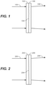
FIG. 1 depicts a blurring element with a substantially random surface as made in accordance with not forming part of the present invention. -
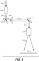
FIG. 2 depicts a blurring element with a substantially regular surface as made in accordance with the principles of the present application -
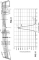
FIG. 3 shows one possible example of a dual modulator projector display system suitable for the purposes of the present application. -
FIG. 4 depicts one embodiment of a blurring element made in accordance with the principles of the present application. -
FIG. 5 depicts yet another example of a projector system not forming part of the present invention. -
FIG. 6 depicts a possible point spread function of the light as potentially produced at the second/later modulator. -
FIG. 7A-1 and 7A-2 depict one example of a blurring element in perspective view and cross-sectional view, respectively, not forming part of the invention. -
FIG. 7B-1 and 7B-2 depict another example of a blurring element in perspective view and cross-sectional view, respectively, not forming part of the present invention. -
FIG. 7C-1 and 7C-2 depict yet another example of a blurring element in perspective view and cross-sectional view, respectively, not forming part of the present invention. -
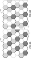
FIGS. 8A and 8B depict two possible examples of blurring elements comprising various patterns of surface features not forming part of the present invention. -
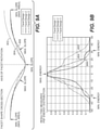
FIGS. 9A and 9B depict possible shapes of concave features and their associated calculated point spread functions, respectively. -
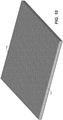
FIG. 10 depicts one example of a blurring element having a somewhat randomized surface variation thereof, not forming part of the present invention. -
FIG. 11 depicts yet another example of a projector system not forming part of the present invention. - As utilized herein, terms "component," "system," "interface," and the like are intended to refer to a computer-related entity (when the context of the discussion is computer-related in nature), either hardware, software (e.g., in execution), and/or firmware. For example, a component can be a process running on a processor, a processor, an object, an executable, a program, and/or a computer. By way of illustration, both an application running on a server and the server can be a component. One or more components can reside within a process and a component can be localized on one computer and/or distributed between two or more computers. A component may also be intended to refer to a communications-related entity, either hardware, software (e.g., in execution), and/or firmware and may further comprise sufficient wired or wireless hardware to affect communications.
- Throughout the following description, specific details are set forth in order to provide a more thorough understanding to persons skilled in the art. However, well known elements may not have been shown or described in detail to avoid unnecessarily obscuring the disclosure. Accordingly, the description and drawings are to be regarded in an illustrative, rather than a restrictive, sense.
- In the field of projector and other display systems, it is desirable to improve both image rendering performance and system efficiency. Systems, methods and techniques are described to affect these improvements by employing light field modeling for dual, or multi-modulation display systems. Light source models are developed and used to advantageous effect. Camera pictures of displayed images of known input images may be evaluated to improve light models. An iterative process may accumulate improvements. These techniques may be used on moving images to make live adjustments to improve image rendering performance.
- Dual modulation projector and display systems have been described in commonly-owned patents and patent applications, including:
- (1)
United States Patent Number 8,125,702 to Ward et al., issued on February 28, 2012 and entitled "SERIAL MODULATION DISPLAY HAVING BINARY LIGHT MODULATION STAGE"; - (2)
United States Patent Application 20130148037 to Whitehead et al., published on June 13, 2013 and entitled "PROJECTION DISPLAYS"; - (3)
United States Patent Application 20110227900 to Wallener, published on September 22, 2011 and entitled "CUSTOM PSFs USING CLUSTERED LIGHT SOURCES"; - (4)
United States Patent Application 20130106923 to Shields et al., published on May 2, 2013 and entitled "SYSTEMS AND METHODS FOR ACCURATELY REPRESENTING HIGH CONTRAST IMAGERY ON HIGH DYNAMIC RANGE DISPLAY SYSTEMS"; - (5)
United States Patent Application 20110279749 to Erinjippurath et al., published on November 17, 2011 and entitled "HIGH DYNAMIC RANGE DISPLAYS USING FILTERLESS LCD(S) FOR INCREASING CONTRAST AND RESOLUTION" and - (6)
United States Patent Application 20120133689 to Kwong, published on May 31, 2012 and entitled "REFLECTORS WITH SPATIALLY VARYING REFLECTANCE/ABSORPTION GRADIENTS FOR COLOR AND LUMINANCE COMPENSATION". - In general, a projector with a single Digital Micromirror Device (DMD) may tend to have a limited contrast ratio. To obtain a greater contrast ratio, two or more DMDs and/or other reflectors (e.g., MEMS) may be arranged in series. As a DMD may operate as a time-division or pulse-width modulator, operating two or more DMDs and/or reflectors in seriesboth acting as pulse-width modulators - tends to require precise time-division alignment and pixel-to-pixel correspondence of time-division sequencing. Such alignment and correspondence requirements may be difficult in practice. Thus, projector and/or display systems may employ different dual-modulation schemes to affect the desired performance.
- For merely one example,
FIG. 3 shows a projector display system that comprises: light 300 (e.g. from a light source - e.g., an array of individually controllable LEDs, lamps, partially coherent light sources, or any light source known in the art), an integrating rod 302 (e.g., that may be used for light recycling purposes, send light 304 further downstream), a first modulator 306 (e.g., a first DMD/modulator) as a "pre-modulator" or "premod" - that may spatially modulate light 304 by means of a halftone image that may be maintained for a desired period of time (e.g., a frame or a portion thereof) to produceintermediate light 308. -
Light 308 may illuminate ablurring element 310, as will be discussed in detail herein. Blurringelement 310 may blur this halftone image to create a spatially-reduced-bandwidth light field 312 that may be applied to a second DMD/modulator 314. The second DMD/modulator -- referred to as the primary modulator -- may further process this light - e.g., pulse-width modulate the blurred light field. This arrangement may tend to avoid both requirements mentioned above - e.g., the precise time-division alignment and/or the pixel-to-pixel correspondence. The two or more DMDs/modulator may be frame-aligned in time, and approximately spatially frame-aligned. The blurred light field from the premod DMD/modulator may substantially overlap the primary DMD/modulator. The spatial alignment may be known and accounted for - e.g., to aid in image rendering performance.Light 316 from the second modulator may be input into otheroptical components 318 to further process the light 316 forfinal projection light 320 ontoviewing screen 322. - It will be appreciated that several components of the projector system may be under control of a controller/processor, in communication with computer-readable media (e.g., RAM, ROM, DVD, CD, flash memory or the like) that stores computer readable instructions that cause the processor to read input image/video data, process that data, send control signals to various components (e.g., light sources, first modulator, second modulator, other modulators) to form a desired projected image, as is known in the art. The controller may receive video/image data and sent control signals to control the light source(s), the first modulator, the second modulator, the blurring element (if there is an actuator or motor control) - e.g., to form the final projected images/video.
- There may be lenses and other optical elements in the light path throughout the projector system - e.g., in
light path first modulator 306. - While the present application is presented in the context of a dual, multi-modulation projection system, it should be appreciated that the techniques and methods of the present application will find application in single modulation, or other dual, multi-modulation display systems. For example, a dual modulation display system comprising a backlight, a first modulator (e.g., LCD or the like), and a second modulator (e.g., LCD or the like) may employ suitable blurring optical components and image processing methods and techniques to affect the performance and efficiencies discussed herein in the context of the projection systems.
- It should also be appreciated that - even though
FIG. 3 depicts a two-stage or dual modulator display system - the methods and techniques of the present application may also find application in a display system with only one modulator or a display system with three or more modulator (multi-modulator) display systems. - As mentioned above, a blurring element may be introduced into the light path in a projector display system. As will be discussed further herein, a blurring element may provide a desired amount of spreading of the light for various reasons - e.g., to provide a desired light spot shape. The blurring element may provide a substantially Gaussian light spot shape coming from the first modulator to illuminate a portion of the second modulator.
- The blurring
element 310 is a lenslet array having certain characteristics in its light shaping ability. The blurring element includes a immersed optical components which is an immersed lenslet array.FIG. 1 shows a comparative example not forming part of the invention example of such acomponent 310. Twoplates interface 104 between the twoplates - The two plates (102 and 106) may be of the same material (e.g., glass, plastic or some other transmissive/translucent material). The two plates comprise materials with a difference of the index of refraction in the range of 0.1 to less than 0.01. This would compare, in distinction, with the difference of index of refraction between a material and air - e.g., typically on the order of 0.5 difference in index of refraction. Such a design of a
component 310 where the diffusion is primarily occurring at a surface between two materials would be called an "immersed" design. - Returning to
FIG. 1 , the diffusing/diffusive surface 104 is immersed between the twoplates surface 104 is substantially irregular.FIG. 10 is a perspective view of a portion of the blurring element. As may be seen, one plate (e.g. 102) may be machined and/or etched to affect a substantially irregular surface/interface 104. To complete the blurring element, the blurring element may be coated and/or encapsulated with an epoxy - or may be mated to another plate (e.g., 106 - not shown inFIG. 10 ) - to complete the blurring element in an immersed design. - It will be appreciated that while the embodiment herein is of the immersed design, it may be possible to create a surface of desired variance such that an air interface may give the desired amount of diffusion to effect a desired PSF shaped light spot in a comparative example not forming part of the invention.
-
FIG. 2 is is the embodiment ofcomponent 310 wherein twoplates output light 208. It should be appreciated that thecomponent 310 comprises one plate in an immersing medium.Component 310 comprises two or more plates with an immersing medium. - The substantially regular interface pattern may take many different configurations.
FIG. 4 is a perspective view of a partial plate inFIG. 2 - and shows one possible configuration of a pattern suitable for the purposes of the present application. As may be seen,plate 202 may be patterned with a set ofconcave features 204 to form the surface interface. As shown, the shape of the features is rectangular. Other features shapes not within the scope of the invention may be possible - e.g., hexagonal, other polygons, circular, or any other shapes. - In addition, while the features of
plate 202 inFIG. 4 are shown as primarily concave (e.g., from machining, etching or the like), it will be appreciated that the features may be convex (e.g., from some form of manufacturing, deposition, formation or the like). - In the embodiment of the present invention, the surface comprises a set of rectangular toroidal lenses with substantially the same radius of curvature in the x and y directions. The size of each lenslet may be on the order of 1 mm. In addition, the curvature may be in the range of 10 to 100 mm.
- As previously mentioned, the blurring element and/or
component 310 may be placed at various points in the optical path. For example,FIG. 5 shows a suitableoptical system 500 for a projector system suitable for the purposes of the present application.System 500 may comprise afirst modulator 502, some intermediate optical components (as shown) and asecond modulator 504. The arrows designated as "1", "2", "3" and "4" are all suitable places within the optical system where a blurring element may be placed in order to affect the desired amount of diffusion - e.g., to affect a desired PSF curve for light spots formed on thesecond modulator 504. It should be appreciated that a suitable blurring element may be placed within the system at other points in the optical pathway. -
FIG. 6 is one example of a possible PSF shape of a light spot produced by an exemplary blurring element described herein. PSF curve 602 may be substantially Gaussian shaped, as shown. Of course, curve 602 may exhibit features that are not precisely Gaussian. For example, curve 602 exhibits a peaked feature 604 - in addition, thebase region 606 may exhibit ripple features that also deviate from an ideal Gaussian spot. These features may be desirable over time and during the course of operation. -
FIGS. 7A-1, 7B-1 and 7C-1 depicted other possible examples of blurring element that may be suitable for the purposes of the present application.FIGS. 7A-2, 7B-2 and 7C-2 depict cross-section views of theFIGS. 7A-1, 7B-1 and 7C-1 , as will be described herein. - The blurring element of
FIG. 7A-1 may comprise aplate 702a having concave (or convex) features in whatever shape desired (e.g., hexagonal, polygonal or the like). As seen inFIG. 7A-2 , anotherplate 704a may be mated to plate 702a by an epoxy and/orsuitable adhesive 706a.Plate 704a may have a flat surface to match the surface ofplate 702a. The features may have a desired sagittal amount (e.g., -0.1 mm as shown - or any other sagittal). The horizontal dimension may be of a desired length (e.g., 4mm as shown - or any other desired amount). -
FIG. 7B-1 may be a blurring element that comprises substantially concentric circular features as shown.FIG. 7B-2 shows possible dimensions - andplate 702b may be matched with a substantially flat plate (not shown) as inFIG. 7A-2 . Alternatively,plate 702b may be passivated, coated and/or encapsulated by an epoxy, adhesive layer or the like (e.g., 704b). Of course, all embodiments herein may comprise such a layer - or not -- as desired. -
FIG. 7C-1 depicts an exemplary blurring element that may comprise aplate 702c with concave features to be geometrically matched with aplate 704c with convex features, as shown. These plates may be mated by an epoxy, adhesive or the like aslayer 706c, if desired. -
FIGS. 8A and 8B are yet other examples of blurringelements - For example, in
FIGS. 8A and 8B , it may be desired to machine, etch and/or pattern with varying sagittal dimensions. One example useful for understanding the invention may have a first, deepsagittal dimension 804, a second, mediumsagittal dimension 806 and a third, slightsagittal dimension 808. It should be appreciated that other dimensions may be possible and/or desired - as well as other feature dimensions (e.g., horizontal) may be varied similarly. As may also be seen, such varied features may be placed on the plate in an array fashion and/or hex pattern. Other patterns of feature placement may be possible and/or desired. -
FIG 9A depicts three possible feature shapes (902, 904 and 906) and/or facet designs - whileFIG. 9B depicts the corresponding estimated PSF shapes 908, 910 and 912 respectively. - As may be seen, for
facet design 902, the feature design comprises the greatest amount of variation - whiledesigns - As may be seen, the PSF shapes 908, 910 and 912 are shown in
FIG. 9B . Each PSF shape represents some deviation from an ideal Gaussian shape. Forexample Facet design 906 has a gradual slope that results in PSF shape 912 that is narrower than the target Gaussian shape.Facet design 902 has higher slopes that result in broader PSF shape 908, but still not matching the target Gaussian shape because it has a narrower peak at the top and broader shoulders at the bottom.Facet design 904 is constructed with spline fits that are betweenfacet design - As creating a substantially random diffusion may be desired to mimic an ideal Gaussian, other examples of the present system may comprise some mechanical motor to produce some motion or oscillation in the blurring element during imaging operation. For example, the blurring element may be made to rotate - or at least oscillate - so that any regular pattern for manufactured features do not show static structure on the PSF shapes as images are being projected through the system. In addition, a combination of lens adjustment and blurring element may also allow for the desired amount of PSF tuning for a desired shaped spot.
- The present use of a blurring element and/or PSF shaping diffusion may be employed to. (1) avoid thermal drift, alignment changes, or other changes in time, (2) avoid the problem of making a standard diffuser with very small diffusion angles and Gaussian PSF, and (3) potentially easier PSF tuning by swapping out known blurring elements with different amounts of spreading.
-
FIG. 11 is an alternative example to the optical system, similar to that shown inFIG. 5 .FIG. 11 incorporates an intermediate image plane where the modulators are imaged in free space - which also allows a blurring element to be located near an image plane. - For example, if a blurring element (i.e., the thick diagonal line shown at or near 1108) is placed near this image plane, then a conventional easy to manufacture diffuser could be used for the blurring element rather than the rather esoteric element needed without the intermediate image plane. The size of the PSF can be adjusted by moving the diffuser closer or further from the intermediate image plane, and the
imaging system 1100 does not need to have an offset focus and a known spherical aberration at the offset focal position. The optical system ofFIG. 11 may comprise: First modulator 1102 (e.g., DLP),lenses 1104, 1106 (formingintermediate image plane 1108, which may be telecentric). The thin diagonal line (near 1108) is the intermediate image plane.Lenses modulator 1114. - This example may employ a more complex relay imaging optical system, since the first modulator is imaged two times rather than just once. However, using the blurring element at the intermediate allows an image system with potentially less stringent requirements, such that it becomes practical without resorting to using double the number of elements of a single relay system. There is often times no need for a focus offset, and the aberrations may be minimized at focus like a conventional optical system.
- A detailed description of one or more embodiments of the invention, read along with accompanying figures, that illustrate the principles of the invention has now been given. It is to be appreciated that the invention is described in connection with such embodiments, but the invention is not limited to any embodiment. The scope of the invention is limited only by the claims.
- Numerous specific details have been set forth in this description in order to provide a thorough understanding of the invention. These details are provided for the purpose of example and the invention may be practiced according to the claims without some or all of these specific details. For the purpose of clarity, technical material that is known in the technical fields related to the invention has not been described in detail so that the invention is not unnecessarily obscured.
Claims (1)
- A blurring element, said blurring element comprises:a first plate (202), said first plate comprising a first transmissive material, the first transmissive material comprising a first surface, and said first surface comprising an interface pattern (204); anda second material, wherein the second material is an immersing material, said second material comprising a second transmissive material comprising a second surface, the second surface in optical communication with the first surface;wherein the first transmissive material comprises a material of different index of refraction than the second transmissive material,and wherein the difference of the index of refraction between the first transmissive material and the second transmissive material is in the range of 0.1 to less than 0.01 characterized in that the interface pattern comprises a set of rectangular toroidal lenses with substantially the same radius of curvature in the x and y directions.
Applications Claiming Priority (3)
| Application Number | Priority Date | Filing Date | Title |
|---|---|---|---|
| US201562162587P | 2015-05-15 | 2015-05-15 | |
| US201662281146P | 2016-01-20 | 2016-01-20 | |
| PCT/US2016/031666 WO2016186900A1 (en) | 2015-05-15 | 2016-05-10 | Control of light spreading with blurring element in projector systems |
Publications (2)
| Publication Number | Publication Date |
|---|---|
| EP3295666A1 EP3295666A1 (en) | 2018-03-21 |
| EP3295666B1 true EP3295666B1 (en) | 2022-02-16 |
Family
ID=56087521
Family Applications (1)
| Application Number | Title | Priority Date | Filing Date |
|---|---|---|---|
| EP16725981.1A Active EP3295666B1 (en) | 2015-05-15 | 2016-05-10 | Control of light spreading with blurring element in projector systems |
Country Status (4)
| Country | Link |
|---|---|
| US (2) | US10326967B2 (en) |
| EP (1) | EP3295666B1 (en) |
| ES (1) | ES2911308T3 (en) |
| WO (1) | WO2016186900A1 (en) |
Families Citing this family (4)
| Publication number | Priority date | Publication date | Assignee | Title |
|---|---|---|---|---|
| CN110313176A (en) * | 2017-02-27 | 2019-10-08 | 索尼公司 | Image processing apparatus, method and program |
| CN110874006B (en) * | 2018-09-03 | 2021-12-21 | 深圳光峰科技股份有限公司 | Light source system and control method thereof, and display device and control method thereof |
| CN114758054A (en) * | 2022-02-23 | 2022-07-15 | 维沃移动通信有限公司 | Light spot adding method, device, equipment and storage medium |
| CN116774501A (en) * | 2022-03-09 | 2023-09-19 | 中强光电股份有限公司 | Projection device and projection method thereof |
Citations (3)
| Publication number | Priority date | Publication date | Assignee | Title |
|---|---|---|---|---|
| JP2009042373A (en) * | 2007-08-07 | 2009-02-26 | Seiko Epson Corp | projector |
| WO2015054032A1 (en) * | 2013-10-10 | 2015-04-16 | Dolby Laboratories Licensing Corporation | Displaying dci and other content on an enhanced dynamic range projector |
| WO2015156120A1 (en) * | 2014-04-07 | 2015-10-15 | ナルックス株式会社 | Optical element |
Family Cites Families (39)
| Publication number | Priority date | Publication date | Assignee | Title |
|---|---|---|---|---|
| DE627460C (en) | 1936-03-16 | Ihagee Kamerawerk Steenbergen | Focusing screen for photographic purposes | |
| ES2813107T3 (en) | 2001-02-27 | 2021-03-22 | Dolby Laboratories Licensing Corp | Procedure and device for displaying an image |
| US6594090B2 (en) * | 2001-08-27 | 2003-07-15 | Eastman Kodak Company | Laser projection display system |
| KR100744892B1 (en) | 2003-03-28 | 2007-08-01 | 세이코 엡슨 가부시키가이샤 | Spatial light modulation device and projector with this spatial light modulation device |
| JP4182032B2 (en) | 2004-07-30 | 2008-11-19 | キヤノン株式会社 | Display optical system and image projection apparatus |
| KR100745869B1 (en) | 2004-10-15 | 2007-08-02 | 세이코 엡슨 가부시키가이샤 | Image display device and projector |
| JP2006251659A (en) | 2005-03-14 | 2006-09-21 | Fuji Photo Film Co Ltd | Viewing angle expansion film and display device using the viewing angle expansion film |
| JP4241776B2 (en) * | 2006-07-21 | 2009-03-18 | セイコーエプソン株式会社 | Image display device |
| TWI295355B (en) | 2006-08-30 | 2008-04-01 | Ind Tech Res Inst | Optical diffusion module and method of manufacturing optical diffusion structure |
| US20140098351A1 (en) * | 2007-07-30 | 2014-04-10 | Imax Corporation | Multiple Source High Performance Stereographic Projection System |
| KR100916304B1 (en) * | 2007-11-26 | 2009-09-10 | 엘지전자 주식회사 | Optical sheet |
| US7551341B1 (en) | 2008-01-28 | 2009-06-23 | Dolby Laboratories Licensing Corporation | Serial modulation display having binary light modulation stage |
| US20090296022A1 (en) | 2008-05-28 | 2009-12-03 | Junghoon Lee | Optical sheet, backlight unit, and liquid crystal display |
| JP5493483B2 (en) | 2008-07-24 | 2014-05-14 | セイコーエプソン株式会社 | projector |
| DE102008047969B4 (en) | 2008-09-18 | 2010-08-12 | Leica Camera Ag | Mirror arrangement for reflex cameras |
| US7988295B2 (en) | 2008-10-28 | 2011-08-02 | Heidelberg Engineering Gmbh | Laser control with phase plate feedback |
| WO2010056618A1 (en) | 2008-11-14 | 2010-05-20 | Dolby Laboratories Licensing Corporation | Custom psfs using clustered light sources |
| WO2011022170A1 (en) | 2009-08-18 | 2011-02-24 | Dolby Laboratories Licensing Corporation | Reflectors with spatially varying reflectance/absorption gradients for color and luminance compensation |
| US9864243B2 (en) | 2010-05-14 | 2018-01-09 | Dolby Laboratories Licensing Corporation | High dynamic range displays using filterless LCD(s) for increasing contrast and resolution |
| US9135864B2 (en) | 2010-05-14 | 2015-09-15 | Dolby Laboratories Licensing Corporation | Systems and methods for accurately representing high contrast imagery on high dynamic range display systems |
| WO2011161931A1 (en) | 2010-06-22 | 2011-12-29 | パナソニック株式会社 | Laser projector |
| CN103430553B (en) | 2011-03-14 | 2016-08-31 | 杜比实验室特许公司 | Display device and method for generating images |
| JP2012234393A (en) * | 2011-05-02 | 2012-11-29 | Sony Corp | Image processing device, image processing method, and program |
| CN102313244A (en) | 2011-09-09 | 2012-01-11 | 中国科学院宁波材料技术与工程研究所湖州新能源产业创新中心 | Light emitting diode (LED) lamp optical lens |
| US20130194644A1 (en) * | 2012-01-30 | 2013-08-01 | Light Blue Optics Ltd | Image display systems |
| US8860640B2 (en) | 2012-05-30 | 2014-10-14 | Christie Digital Systems Usa, Inc. | Zonal illumination for high dynamic range projection |
| US10553002B2 (en) * | 2012-08-31 | 2020-02-04 | Apple, Inc. | Information display using electronic diffusers |
| CN106647124A (en) | 2013-02-04 | 2017-05-10 | 深圳市光峰光电技术有限公司 | Laser light source, wavelength conversion light source, light composition light source and projection display equipment |
| US9224323B2 (en) * | 2013-05-06 | 2015-12-29 | Dolby Laboratories Licensing Corporation | Systems and methods for increasing spatial or temporal resolution for dual modulated display systems |
| CN105158913B (en) | 2013-05-13 | 2019-06-21 | 深圳光峰科技股份有限公司 | Laser light source, wavelength conversion light source, combined light source and projection system |
| US9049413B2 (en) | 2013-07-30 | 2015-06-02 | Dolby Laboratories Licensing Corporation | Multiple stage modulation projector display systems having efficient light utilization |
| WO2015023762A2 (en) | 2013-08-16 | 2015-02-19 | Dolby Laboratories Licensing Corporation | Systems and methods for light field modeling techniques for multi-modulation displays |
| EP4236287B1 (en) | 2013-11-03 | 2025-08-06 | Dolby Laboratories Licensing Corporation | Local dimming in multi-modulation displays |
| US9188767B2 (en) | 2013-11-04 | 2015-11-17 | Christie Digital Systems Usa, Inc. | Relay lens system for a high dynamic range projector |
| US9232172B2 (en) | 2013-11-04 | 2016-01-05 | Christie Digital Systems Usa, Inc. | Two-stage light modulation for high dynamic range |
| US20150124330A1 (en) | 2013-11-04 | 2015-05-07 | Christie Digital Systems Canada Inc. | Relay lens system for a high dynamic range projector |
| JP6471424B2 (en) | 2013-11-13 | 2019-02-20 | セイコーエプソン株式会社 | projector |
| JP2015102614A (en) * | 2013-11-22 | 2015-06-04 | セイコーエプソン株式会社 | Display device |
| US10386709B2 (en) | 2014-12-31 | 2019-08-20 | Dolby Laboratories Licensing Corporation | Methods and systems for high dynamic range image projectors |
-
2016
- 2016-05-10 US US15/574,017 patent/US10326967B2/en active Active
- 2016-05-10 ES ES16725981T patent/ES2911308T3/en active Active
- 2016-05-10 WO PCT/US2016/031666 patent/WO2016186900A1/en not_active Ceased
- 2016-05-10 EP EP16725981.1A patent/EP3295666B1/en active Active
-
2019
- 2019-05-03 US US16/403,287 patent/US10659739B2/en active Active
Patent Citations (4)
| Publication number | Priority date | Publication date | Assignee | Title |
|---|---|---|---|---|
| JP2009042373A (en) * | 2007-08-07 | 2009-02-26 | Seiko Epson Corp | projector |
| WO2015054032A1 (en) * | 2013-10-10 | 2015-04-16 | Dolby Laboratories Licensing Corporation | Displaying dci and other content on an enhanced dynamic range projector |
| WO2015156120A1 (en) * | 2014-04-07 | 2015-10-15 | ナルックス株式会社 | Optical element |
| US20170045648A1 (en) * | 2014-04-07 | 2017-02-16 | Nalux Co., Ltd. | Microlens array |
Non-Patent Citations (1)
| Title |
|---|
| ANONYMOUS: "Toric lens - Wikipedia", 11 April 2015 (2015-04-11), XP055717981, Retrieved from the Internet <URL:https://en.wikipedia.org/w/index.php?title=Toric_lens&oldid=655927124> [retrieved on 20200724] * |
Also Published As
| Publication number | Publication date |
|---|---|
| US10326967B2 (en) | 2019-06-18 |
| WO2016186900A1 (en) | 2016-11-24 |
| EP3295666A1 (en) | 2018-03-21 |
| US10659739B2 (en) | 2020-05-19 |
| ES2911308T3 (en) | 2022-05-18 |
| US20180295329A1 (en) | 2018-10-11 |
| US20190260975A1 (en) | 2019-08-22 |
Similar Documents
| Publication | Publication Date | Title |
|---|---|---|
| US11598966B2 (en) | Light projection system including an optical assembly for correction of differential distortion | |
| CN102428402B (en) | Projection with lenslet arrangement on speckle reduction element | |
| JP4407585B2 (en) | LIGHTING DEVICE, IMAGE DISPLAY DEVICE, AND PROJECTOR | |
| CN102483523B (en) | Optical laser projection system with speckle reduction element configured for out-of-plane movement | |
| US10659739B2 (en) | Control of light spreading with blurring element in projector systems | |
| US9170474B2 (en) | Efficient spatially modulated illumination system | |
| US20180149869A1 (en) | Apparatus and Method for Near Eye Display | |
| JP2012527645A5 (en) | ||
| RU2013156243A (en) | PROJECTIVE DISPLAY DEVICE AND METHOD FOR DISPLAYING A FULL IMAGE FOR PROJECTIVE SURFACES OF AN ARBITRARY FORM OR INCLINED PROJECTION SURFACES | |
| JPH08327900A (en) | Offset zoom lens for reflected light modulator | |
| CN101109890A (en) | image display device | |
| US20240089416A1 (en) | Multiplexing light field display | |
| JP2024505088A (en) | Projection system and method with dynamic target geometry | |
| JPH03216638A (en) | Projection type display device | |
| US20020101657A1 (en) | Stereoscopic display device | |
| JP6669812B2 (en) | Acousto-optic beam steering modulator for projection systems | |
| JP2004004256A (en) | Optical scanning device and two-dimensional image forming device | |
| US7883219B2 (en) | System and method for displaying images | |
| JP4598409B2 (en) | Display device and projection display device | |
| KR200315584Y1 (en) | Optical system of projecting apparatus | |
| KR101315981B1 (en) | Projector | |
| WO2006020583A3 (en) | Imaging material with improved contrast | |
| US20180275408A1 (en) | Head-mounted display apparatus | |
| US20250355322A1 (en) | Projector lens apertures for projection systems | |
| CN103293843B (en) | Polarization conversion element group for projection device and projection device |
Legal Events
| Date | Code | Title | Description |
|---|---|---|---|
| STAA | Information on the status of an ep patent application or granted ep patent |
Free format text: STATUS: THE INTERNATIONAL PUBLICATION HAS BEEN MADE |
|
| PUAI | Public reference made under article 153(3) epc to a published international application that has entered the european phase |
Free format text: ORIGINAL CODE: 0009012 |
|
| STAA | Information on the status of an ep patent application or granted ep patent |
Free format text: STATUS: REQUEST FOR EXAMINATION WAS MADE |
|
| 17P | Request for examination filed |
Effective date: 20171215 |
|
| AK | Designated contracting states |
Kind code of ref document: A1 Designated state(s): AL AT BE BG CH CY CZ DE DK EE ES FI FR GB GR HR HU IE IS IT LI LT LU LV MC MK MT NL NO PL PT RO RS SE SI SK SM TR |
|
| AX | Request for extension of the european patent |
Extension state: BA ME |
|
| DAV | Request for validation of the european patent (deleted) | ||
| DAX | Request for extension of the european patent (deleted) | ||
| STAA | Information on the status of an ep patent application or granted ep patent |
Free format text: STATUS: EXAMINATION IS IN PROGRESS |
|
| 17Q | First examination report despatched |
Effective date: 20190515 |
|
| REG | Reference to a national code |
Ref country code: DE Ref legal event code: R079 Ref document number: 602016069130 Country of ref document: DE Free format text: PREVIOUS MAIN CLASS: H04N0005740000 Ipc: G02B0005020000 |
|
| GRAP | Despatch of communication of intention to grant a patent |
Free format text: ORIGINAL CODE: EPIDOSNIGR1 |
|
| STAA | Information on the status of an ep patent application or granted ep patent |
Free format text: STATUS: GRANT OF PATENT IS INTENDED |
|
| RIC1 | Information provided on ipc code assigned before grant |
Ipc: H04N 9/31 20060101ALI20210805BHEP Ipc: G03B 21/00 20060101ALI20210805BHEP Ipc: H04N 5/74 20060101ALI20210805BHEP Ipc: G02B 5/02 20060101AFI20210805BHEP |
|
| INTG | Intention to grant announced |
Effective date: 20210901 |
|
| GRAS | Grant fee paid |
Free format text: ORIGINAL CODE: EPIDOSNIGR3 |
|
| GRAA | (expected) grant |
Free format text: ORIGINAL CODE: 0009210 |
|
| STAA | Information on the status of an ep patent application or granted ep patent |
Free format text: STATUS: THE PATENT HAS BEEN GRANTED |
|
| AK | Designated contracting states |
Kind code of ref document: B1 Designated state(s): AL AT BE BG CH CY CZ DE DK EE ES FI FR GB GR HR HU IE IS IT LI LT LU LV MC MK MT NL NO PL PT RO RS SE SI SK SM TR |
|
| REG | Reference to a national code |
Ref country code: GB Ref legal event code: FG4D |
|
| REG | Reference to a national code |
Ref country code: CH Ref legal event code: EP |
|
| REG | Reference to a national code |
Ref country code: DE Ref legal event code: R096 Ref document number: 602016069130 Country of ref document: DE |
|
| REG | Reference to a national code |
Ref country code: AT Ref legal event code: REF Ref document number: 1469239 Country of ref document: AT Kind code of ref document: T Effective date: 20220315 |
|
| REG | Reference to a national code |
Ref country code: IE Ref legal event code: FG4D |
|
| REG | Reference to a national code |
Ref country code: NL Ref legal event code: FP |
|
| REG | Reference to a national code |
Ref country code: ES Ref legal event code: FG2A Ref document number: 2911308 Country of ref document: ES Kind code of ref document: T3 Effective date: 20220518 |
|
| REG | Reference to a national code |
Ref country code: LT Ref legal event code: MG9D |
|
| REG | Reference to a national code |
Ref country code: AT Ref legal event code: MK05 Ref document number: 1469239 Country of ref document: AT Kind code of ref document: T Effective date: 20220216 |
|
| PG25 | Lapsed in a contracting state [announced via postgrant information from national office to epo] |
Ref country code: SE Free format text: LAPSE BECAUSE OF FAILURE TO SUBMIT A TRANSLATION OF THE DESCRIPTION OR TO PAY THE FEE WITHIN THE PRESCRIBED TIME-LIMIT Effective date: 20220216 Ref country code: RS Free format text: LAPSE BECAUSE OF FAILURE TO SUBMIT A TRANSLATION OF THE DESCRIPTION OR TO PAY THE FEE WITHIN THE PRESCRIBED TIME-LIMIT Effective date: 20220216 Ref country code: PT Free format text: LAPSE BECAUSE OF FAILURE TO SUBMIT A TRANSLATION OF THE DESCRIPTION OR TO PAY THE FEE WITHIN THE PRESCRIBED TIME-LIMIT Effective date: 20220616 Ref country code: NO Free format text: LAPSE BECAUSE OF FAILURE TO SUBMIT A TRANSLATION OF THE DESCRIPTION OR TO PAY THE FEE WITHIN THE PRESCRIBED TIME-LIMIT Effective date: 20220516 Ref country code: LT Free format text: LAPSE BECAUSE OF FAILURE TO SUBMIT A TRANSLATION OF THE DESCRIPTION OR TO PAY THE FEE WITHIN THE PRESCRIBED TIME-LIMIT Effective date: 20220216 Ref country code: HR Free format text: LAPSE BECAUSE OF FAILURE TO SUBMIT A TRANSLATION OF THE DESCRIPTION OR TO PAY THE FEE WITHIN THE PRESCRIBED TIME-LIMIT Effective date: 20220216 Ref country code: BG Free format text: LAPSE BECAUSE OF FAILURE TO SUBMIT A TRANSLATION OF THE DESCRIPTION OR TO PAY THE FEE WITHIN THE PRESCRIBED TIME-LIMIT Effective date: 20220516 |
|
| PG25 | Lapsed in a contracting state [announced via postgrant information from national office to epo] |
Ref country code: PL Free format text: LAPSE BECAUSE OF FAILURE TO SUBMIT A TRANSLATION OF THE DESCRIPTION OR TO PAY THE FEE WITHIN THE PRESCRIBED TIME-LIMIT Effective date: 20220216 Ref country code: LV Free format text: LAPSE BECAUSE OF FAILURE TO SUBMIT A TRANSLATION OF THE DESCRIPTION OR TO PAY THE FEE WITHIN THE PRESCRIBED TIME-LIMIT Effective date: 20220216 Ref country code: GR Free format text: LAPSE BECAUSE OF FAILURE TO SUBMIT A TRANSLATION OF THE DESCRIPTION OR TO PAY THE FEE WITHIN THE PRESCRIBED TIME-LIMIT Effective date: 20220517 Ref country code: FI Free format text: LAPSE BECAUSE OF FAILURE TO SUBMIT A TRANSLATION OF THE DESCRIPTION OR TO PAY THE FEE WITHIN THE PRESCRIBED TIME-LIMIT Effective date: 20220216 Ref country code: AT Free format text: LAPSE BECAUSE OF FAILURE TO SUBMIT A TRANSLATION OF THE DESCRIPTION OR TO PAY THE FEE WITHIN THE PRESCRIBED TIME-LIMIT Effective date: 20220216 |
|
| PG25 | Lapsed in a contracting state [announced via postgrant information from national office to epo] |
Ref country code: IS Free format text: LAPSE BECAUSE OF FAILURE TO SUBMIT A TRANSLATION OF THE DESCRIPTION OR TO PAY THE FEE WITHIN THE PRESCRIBED TIME-LIMIT Effective date: 20220617 |
|
| PG25 | Lapsed in a contracting state [announced via postgrant information from national office to epo] |
Ref country code: SM Free format text: LAPSE BECAUSE OF FAILURE TO SUBMIT A TRANSLATION OF THE DESCRIPTION OR TO PAY THE FEE WITHIN THE PRESCRIBED TIME-LIMIT Effective date: 20220216 Ref country code: SK Free format text: LAPSE BECAUSE OF FAILURE TO SUBMIT A TRANSLATION OF THE DESCRIPTION OR TO PAY THE FEE WITHIN THE PRESCRIBED TIME-LIMIT Effective date: 20220216 Ref country code: RO Free format text: LAPSE BECAUSE OF FAILURE TO SUBMIT A TRANSLATION OF THE DESCRIPTION OR TO PAY THE FEE WITHIN THE PRESCRIBED TIME-LIMIT Effective date: 20220216 Ref country code: EE Free format text: LAPSE BECAUSE OF FAILURE TO SUBMIT A TRANSLATION OF THE DESCRIPTION OR TO PAY THE FEE WITHIN THE PRESCRIBED TIME-LIMIT Effective date: 20220216 Ref country code: DK Free format text: LAPSE BECAUSE OF FAILURE TO SUBMIT A TRANSLATION OF THE DESCRIPTION OR TO PAY THE FEE WITHIN THE PRESCRIBED TIME-LIMIT Effective date: 20220216 Ref country code: CZ Free format text: LAPSE BECAUSE OF FAILURE TO SUBMIT A TRANSLATION OF THE DESCRIPTION OR TO PAY THE FEE WITHIN THE PRESCRIBED TIME-LIMIT Effective date: 20220216 |
|
| REG | Reference to a national code |
Ref country code: DE Ref legal event code: R097 Ref document number: 602016069130 Country of ref document: DE |
|
| PG25 | Lapsed in a contracting state [announced via postgrant information from national office to epo] |
Ref country code: AL Free format text: LAPSE BECAUSE OF FAILURE TO SUBMIT A TRANSLATION OF THE DESCRIPTION OR TO PAY THE FEE WITHIN THE PRESCRIBED TIME-LIMIT Effective date: 20220216 |
|
| PLBE | No opposition filed within time limit |
Free format text: ORIGINAL CODE: 0009261 |
|
| STAA | Information on the status of an ep patent application or granted ep patent |
Free format text: STATUS: NO OPPOSITION FILED WITHIN TIME LIMIT |
|
| REG | Reference to a national code |
Ref country code: CH Ref legal event code: PL |
|
| REG | Reference to a national code |
Ref country code: BE Ref legal event code: MM Effective date: 20220531 |
|
| 26N | No opposition filed |
Effective date: 20221117 |
|
| PG25 | Lapsed in a contracting state [announced via postgrant information from national office to epo] |
Ref country code: MC Free format text: LAPSE BECAUSE OF FAILURE TO SUBMIT A TRANSLATION OF THE DESCRIPTION OR TO PAY THE FEE WITHIN THE PRESCRIBED TIME-LIMIT Effective date: 20220216 Ref country code: LU Free format text: LAPSE BECAUSE OF NON-PAYMENT OF DUE FEES Effective date: 20220510 Ref country code: LI Free format text: LAPSE BECAUSE OF NON-PAYMENT OF DUE FEES Effective date: 20220531 Ref country code: CH Free format text: LAPSE BECAUSE OF NON-PAYMENT OF DUE FEES Effective date: 20220531 |
|
| PG25 | Lapsed in a contracting state [announced via postgrant information from national office to epo] |
Ref country code: SI Free format text: LAPSE BECAUSE OF FAILURE TO SUBMIT A TRANSLATION OF THE DESCRIPTION OR TO PAY THE FEE WITHIN THE PRESCRIBED TIME-LIMIT Effective date: 20220216 |
|
| PG25 | Lapsed in a contracting state [announced via postgrant information from national office to epo] |
Ref country code: IE Free format text: LAPSE BECAUSE OF NON-PAYMENT OF DUE FEES Effective date: 20220510 |
|
| PG25 | Lapsed in a contracting state [announced via postgrant information from national office to epo] |
Ref country code: BE Free format text: LAPSE BECAUSE OF NON-PAYMENT OF DUE FEES Effective date: 20220531 |
|
| P01 | Opt-out of the competence of the unified patent court (upc) registered |
Effective date: 20230513 |
|
| PG25 | Lapsed in a contracting state [announced via postgrant information from national office to epo] |
Ref country code: HU Free format text: LAPSE BECAUSE OF FAILURE TO SUBMIT A TRANSLATION OF THE DESCRIPTION OR TO PAY THE FEE WITHIN THE PRESCRIBED TIME-LIMIT; INVALID AB INITIO Effective date: 20160510 |
|
| PG25 | Lapsed in a contracting state [announced via postgrant information from national office to epo] |
Ref country code: MK Free format text: LAPSE BECAUSE OF FAILURE TO SUBMIT A TRANSLATION OF THE DESCRIPTION OR TO PAY THE FEE WITHIN THE PRESCRIBED TIME-LIMIT Effective date: 20220216 Ref country code: CY Free format text: LAPSE BECAUSE OF FAILURE TO SUBMIT A TRANSLATION OF THE DESCRIPTION OR TO PAY THE FEE WITHIN THE PRESCRIBED TIME-LIMIT Effective date: 20220216 |
|
| PG25 | Lapsed in a contracting state [announced via postgrant information from national office to epo] |
Ref country code: MT Free format text: LAPSE BECAUSE OF FAILURE TO SUBMIT A TRANSLATION OF THE DESCRIPTION OR TO PAY THE FEE WITHIN THE PRESCRIBED TIME-LIMIT Effective date: 20220216 |
|
| PG25 | Lapsed in a contracting state [announced via postgrant information from national office to epo] |
Ref country code: TR Free format text: LAPSE BECAUSE OF FAILURE TO SUBMIT A TRANSLATION OF THE DESCRIPTION OR TO PAY THE FEE WITHIN THE PRESCRIBED TIME-LIMIT Effective date: 20220216 |
|
| PGFP | Annual fee paid to national office [announced via postgrant information from national office to epo] |
Ref country code: GB Payment date: 20260317 Year of fee payment: 11 |
|
| PGFP | Annual fee paid to national office [announced via postgrant information from national office to epo] |
Ref country code: NL Payment date: 20260421 Year of fee payment: 11 |
|
| PGFP | Annual fee paid to national office [announced via postgrant information from national office to epo] |
Ref country code: ES Payment date: 20260601 Year of fee payment: 11 |
|
| PGFP | Annual fee paid to national office [announced via postgrant information from national office to epo] |
Ref country code: IT Payment date: 20260421 Year of fee payment: 11 |
|
| PGFP | Annual fee paid to national office [announced via postgrant information from national office to epo] |
Ref country code: DE Payment date: 20260421 Year of fee payment: 11 |
|
| PGFP | Annual fee paid to national office [announced via postgrant information from national office to epo] |
Ref country code: FR Payment date: 20260421 Year of fee payment: 11 |