EP3293760A1 - Wafer level semiconductor device with wettable flanks - Google Patents
Wafer level semiconductor device with wettable flanks Download PDFInfo
- Publication number
- EP3293760A1 EP3293760A1 EP17178522.3A EP17178522A EP3293760A1 EP 3293760 A1 EP3293760 A1 EP 3293760A1 EP 17178522 A EP17178522 A EP 17178522A EP 3293760 A1 EP3293760 A1 EP 3293760A1
- Authority
- EP
- European Patent Office
- Prior art keywords
- top surface
- semiconductor device
- metal layer
- die
- package body
- Prior art date
- Legal status (The legal status is an assumption and is not a legal conclusion. Google has not performed a legal analysis and makes no representation as to the accuracy of the status listed.)
- Pending
Links
Images




Classifications
-
- H—ELECTRICITY
- H10—SEMICONDUCTOR DEVICES; ELECTRIC SOLID-STATE DEVICES NOT OTHERWISE PROVIDED FOR
- H10W—GENERIC PACKAGES, INTERCONNECTIONS, CONNECTORS OR OTHER CONSTRUCTIONAL DETAILS OF DEVICES COVERED BY CLASS H10
- H10W74/00—Encapsulations, e.g. protective coatings
- H10W74/10—Encapsulations, e.g. protective coatings characterised by their shape or disposition
- H10W74/111—Encapsulations, e.g. protective coatings characterised by their shape or disposition the semiconductor body being completely enclosed
- H10W74/129—Encapsulations, e.g. protective coatings characterised by their shape or disposition the semiconductor body being completely enclosed forming a chip-scale package [CSP]
-
- H—ELECTRICITY
- H10—SEMICONDUCTOR DEVICES; ELECTRIC SOLID-STATE DEVICES NOT OTHERWISE PROVIDED FOR
- H10W—GENERIC PACKAGES, INTERCONNECTIONS, CONNECTORS OR OTHER CONSTRUCTIONAL DETAILS OF DEVICES COVERED BY CLASS H10
- H10W70/00—Package substrates; Interposers; Redistribution layers [RDL]
- H10W70/60—Insulating or insulated package substrates; Interposers; Redistribution layers
- H10W70/67—Insulating or insulated package substrates; Interposers; Redistribution layers characterised by their insulating layers or insulating parts
- H10W70/69—Insulating materials thereof
-
- H—ELECTRICITY
- H10—SEMICONDUCTOR DEVICES; ELECTRIC SOLID-STATE DEVICES NOT OTHERWISE PROVIDED FOR
- H10P—GENERIC PROCESSES OR APPARATUS FOR THE MANUFACTURE OR TREATMENT OF DEVICES COVERED BY CLASS H10
- H10P54/00—Cutting or separating of wafers, substrates or parts of devices
-
- H—ELECTRICITY
- H10—SEMICONDUCTOR DEVICES; ELECTRIC SOLID-STATE DEVICES NOT OTHERWISE PROVIDED FOR
- H10P—GENERIC PROCESSES OR APPARATUS FOR THE MANUFACTURE OR TREATMENT OF DEVICES COVERED BY CLASS H10
- H10P72/00—Handling or holding of wafers, substrates or devices during manufacture or treatment thereof
- H10P72/70—Handling or holding of wafers, substrates or devices during manufacture or treatment thereof for supporting or gripping
- H10P72/74—Handling or holding of wafers, substrates or devices during manufacture or treatment thereof for supporting or gripping using temporarily an auxiliary support
- H10P72/7402—Wafer tapes, e.g. grinding or dicing support tapes
-
- H—ELECTRICITY
- H10—SEMICONDUCTOR DEVICES; ELECTRIC SOLID-STATE DEVICES NOT OTHERWISE PROVIDED FOR
- H10W—GENERIC PACKAGES, INTERCONNECTIONS, CONNECTORS OR OTHER CONSTRUCTIONAL DETAILS OF DEVICES COVERED BY CLASS H10
- H10W42/00—Arrangements for protection of devices
- H10W42/20—Arrangements for protection of devices protecting against electromagnetic or particle radiation, e.g. light, X-rays, gamma-rays or electrons
-
- H—ELECTRICITY
- H10—SEMICONDUCTOR DEVICES; ELECTRIC SOLID-STATE DEVICES NOT OTHERWISE PROVIDED FOR
- H10W—GENERIC PACKAGES, INTERCONNECTIONS, CONNECTORS OR OTHER CONSTRUCTIONAL DETAILS OF DEVICES COVERED BY CLASS H10
- H10W70/00—Package substrates; Interposers; Redistribution layers [RDL]
- H10W70/01—Manufacture or treatment
- H10W70/05—Manufacture or treatment of insulating or insulated package substrates, or of interposers, or of redistribution layers
- H10W70/093—Connecting or disconnecting other interconnections thereto or therefrom, e.g. connecting bond wires or bumps
-
- H—ELECTRICITY
- H10—SEMICONDUCTOR DEVICES; ELECTRIC SOLID-STATE DEVICES NOT OTHERWISE PROVIDED FOR
- H10W—GENERIC PACKAGES, INTERCONNECTIONS, CONNECTORS OR OTHER CONSTRUCTIONAL DETAILS OF DEVICES COVERED BY CLASS H10
- H10W74/00—Encapsulations, e.g. protective coatings
- H10W74/01—Manufacture or treatment
- H10W74/016—Manufacture or treatment using moulds
-
- H—ELECTRICITY
- H10—SEMICONDUCTOR DEVICES; ELECTRIC SOLID-STATE DEVICES NOT OTHERWISE PROVIDED FOR
- H10W—GENERIC PACKAGES, INTERCONNECTIONS, CONNECTORS OR OTHER CONSTRUCTIONAL DETAILS OF DEVICES COVERED BY CLASS H10
- H10W74/00—Encapsulations, e.g. protective coatings
- H10W74/10—Encapsulations, e.g. protective coatings characterised by their shape or disposition
- H10W74/111—Encapsulations, e.g. protective coatings characterised by their shape or disposition the semiconductor body being completely enclosed
- H10W74/114—Encapsulations, e.g. protective coatings characterised by their shape or disposition the semiconductor body being completely enclosed by a substrate and the encapsulations
-
- H—ELECTRICITY
- H10—SEMICONDUCTOR DEVICES; ELECTRIC SOLID-STATE DEVICES NOT OTHERWISE PROVIDED FOR
- H10W—GENERIC PACKAGES, INTERCONNECTIONS, CONNECTORS OR OTHER CONSTRUCTIONAL DETAILS OF DEVICES COVERED BY CLASS H10
- H10W74/00—Encapsulations, e.g. protective coatings
- H10W74/10—Encapsulations, e.g. protective coatings characterised by their shape or disposition
- H10W74/131—Encapsulations, e.g. protective coatings characterised by their shape or disposition the semiconductor body being only partially enclosed
- H10W74/141—Encapsulations, e.g. protective coatings characterised by their shape or disposition the semiconductor body being only partially enclosed the encapsulations being on at least the sidewalls of the semiconductor body
-
- H—ELECTRICITY
- H10—SEMICONDUCTOR DEVICES; ELECTRIC SOLID-STATE DEVICES NOT OTHERWISE PROVIDED FOR
- H10W—GENERIC PACKAGES, INTERCONNECTIONS, CONNECTORS OR OTHER CONSTRUCTIONAL DETAILS OF DEVICES COVERED BY CLASS H10
- H10W70/00—Package substrates; Interposers; Redistribution layers [RDL]
- H10W70/60—Insulating or insulated package substrates; Interposers; Redistribution layers
- H10W70/62—Insulating or insulated package substrates; Interposers; Redistribution layers characterised by their interconnections
- H10W70/65—Shapes or dispositions of interconnections
-
- H—ELECTRICITY
- H10—SEMICONDUCTOR DEVICES; ELECTRIC SOLID-STATE DEVICES NOT OTHERWISE PROVIDED FOR
- H10W—GENERIC PACKAGES, INTERCONNECTIONS, CONNECTORS OR OTHER CONSTRUCTIONAL DETAILS OF DEVICES COVERED BY CLASS H10
- H10W70/00—Package substrates; Interposers; Redistribution layers [RDL]
- H10W70/60—Insulating or insulated package substrates; Interposers; Redistribution layers
- H10W70/67—Insulating or insulated package substrates; Interposers; Redistribution layers characterised by their insulating layers or insulating parts
- H10W70/69—Insulating materials thereof
- H10W70/698—Semiconductor materials that are electrically insulating, e.g. undoped silicon
-
- H—ELECTRICITY
- H10—SEMICONDUCTOR DEVICES; ELECTRIC SOLID-STATE DEVICES NOT OTHERWISE PROVIDED FOR
- H10W—GENERIC PACKAGES, INTERCONNECTIONS, CONNECTORS OR OTHER CONSTRUCTIONAL DETAILS OF DEVICES COVERED BY CLASS H10
- H10W72/00—Interconnections or connectors in packages
- H10W72/01—Manufacture or treatment
- H10W72/019—Manufacture or treatment of bond pads
- H10W72/01904—Manufacture or treatment of bond pads using temporary auxiliary members, e.g. using sacrificial coatings or handle substrates
-
- H—ELECTRICITY
- H10—SEMICONDUCTOR DEVICES; ELECTRIC SOLID-STATE DEVICES NOT OTHERWISE PROVIDED FOR
- H10W—GENERIC PACKAGES, INTERCONNECTIONS, CONNECTORS OR OTHER CONSTRUCTIONAL DETAILS OF DEVICES COVERED BY CLASS H10
- H10W72/00—Interconnections or connectors in packages
- H10W72/01—Manufacture or treatment
- H10W72/019—Manufacture or treatment of bond pads
- H10W72/01931—Manufacture or treatment of bond pads using blanket deposition
- H10W72/01933—Manufacture or treatment of bond pads using blanket deposition in liquid form, e.g. spin coating, spray coating or immersion coating
- H10W72/01935—Manufacture or treatment of bond pads using blanket deposition in liquid form, e.g. spin coating, spray coating or immersion coating by plating, e.g. electroless plating or electroplating
-
- H—ELECTRICITY
- H10—SEMICONDUCTOR DEVICES; ELECTRIC SOLID-STATE DEVICES NOT OTHERWISE PROVIDED FOR
- H10W—GENERIC PACKAGES, INTERCONNECTIONS, CONNECTORS OR OTHER CONSTRUCTIONAL DETAILS OF DEVICES COVERED BY CLASS H10
- H10W72/00—Interconnections or connectors in packages
- H10W72/01—Manufacture or treatment
- H10W72/019—Manufacture or treatment of bond pads
- H10W72/01931—Manufacture or treatment of bond pads using blanket deposition
- H10W72/01938—Manufacture or treatment of bond pads using blanket deposition in gaseous form, e.g. by CVD or PVD
-
- H—ELECTRICITY
- H10—SEMICONDUCTOR DEVICES; ELECTRIC SOLID-STATE DEVICES NOT OTHERWISE PROVIDED FOR
- H10W—GENERIC PACKAGES, INTERCONNECTIONS, CONNECTORS OR OTHER CONSTRUCTIONAL DETAILS OF DEVICES COVERED BY CLASS H10
- H10W72/00—Interconnections or connectors in packages
- H10W72/01—Manufacture or treatment
- H10W72/0198—Manufacture or treatment batch processes
-
- H—ELECTRICITY
- H10—SEMICONDUCTOR DEVICES; ELECTRIC SOLID-STATE DEVICES NOT OTHERWISE PROVIDED FOR
- H10W—GENERIC PACKAGES, INTERCONNECTIONS, CONNECTORS OR OTHER CONSTRUCTIONAL DETAILS OF DEVICES COVERED BY CLASS H10
- H10W72/00—Interconnections or connectors in packages
- H10W72/071—Connecting or disconnecting
- H10W72/073—Connecting or disconnecting of die-attach connectors
- H10W72/07331—Connecting techniques
-
- H—ELECTRICITY
- H10—SEMICONDUCTOR DEVICES; ELECTRIC SOLID-STATE DEVICES NOT OTHERWISE PROVIDED FOR
- H10W—GENERIC PACKAGES, INTERCONNECTIONS, CONNECTORS OR OTHER CONSTRUCTIONAL DETAILS OF DEVICES COVERED BY CLASS H10
- H10W72/00—Interconnections or connectors in packages
- H10W72/071—Connecting or disconnecting
- H10W72/073—Connecting or disconnecting of die-attach connectors
- H10W72/07331—Connecting techniques
- H10W72/07337—Connecting techniques using a polymer adhesive, e.g. an adhesive based on silicone or epoxy
-
- H—ELECTRICITY
- H10—SEMICONDUCTOR DEVICES; ELECTRIC SOLID-STATE DEVICES NOT OTHERWISE PROVIDED FOR
- H10W—GENERIC PACKAGES, INTERCONNECTIONS, CONNECTORS OR OTHER CONSTRUCTIONAL DETAILS OF DEVICES COVERED BY CLASS H10
- H10W72/00—Interconnections or connectors in packages
- H10W72/20—Bump connectors, e.g. solder bumps or copper pillars; Dummy bumps; Thermal bumps
- H10W72/281—Auxiliary members
- H10W72/287—Flow barriers
-
- H—ELECTRICITY
- H10—SEMICONDUCTOR DEVICES; ELECTRIC SOLID-STATE DEVICES NOT OTHERWISE PROVIDED FOR
- H10W—GENERIC PACKAGES, INTERCONNECTIONS, CONNECTORS OR OTHER CONSTRUCTIONAL DETAILS OF DEVICES COVERED BY CLASS H10
- H10W72/00—Interconnections or connectors in packages
- H10W72/20—Bump connectors, e.g. solder bumps or copper pillars; Dummy bumps; Thermal bumps
- H10W72/29—Bond pads specially adapted therefor
-
- H—ELECTRICITY
- H10—SEMICONDUCTOR DEVICES; ELECTRIC SOLID-STATE DEVICES NOT OTHERWISE PROVIDED FOR
- H10W—GENERIC PACKAGES, INTERCONNECTIONS, CONNECTORS OR OTHER CONSTRUCTIONAL DETAILS OF DEVICES COVERED BY CLASS H10
- H10W72/00—Interconnections or connectors in packages
- H10W72/30—Die-attach connectors
- H10W72/321—Structures or relative sizes of die-attach connectors
- H10W72/325—Die-attach connectors having a filler embedded in a matrix
-
- H—ELECTRICITY
- H10—SEMICONDUCTOR DEVICES; ELECTRIC SOLID-STATE DEVICES NOT OTHERWISE PROVIDED FOR
- H10W—GENERIC PACKAGES, INTERCONNECTIONS, CONNECTORS OR OTHER CONSTRUCTIONAL DETAILS OF DEVICES COVERED BY CLASS H10
- H10W72/00—Interconnections or connectors in packages
- H10W72/30—Die-attach connectors
- H10W72/351—Materials of die-attach connectors
- H10W72/353—Materials of die-attach connectors not comprising solid metals or solid metalloids, e.g. ceramics
- H10W72/354—Materials of die-attach connectors not comprising solid metals or solid metalloids, e.g. ceramics comprising polymers
-
- H—ELECTRICITY
- H10—SEMICONDUCTOR DEVICES; ELECTRIC SOLID-STATE DEVICES NOT OTHERWISE PROVIDED FOR
- H10W—GENERIC PACKAGES, INTERCONNECTIONS, CONNECTORS OR OTHER CONSTRUCTIONAL DETAILS OF DEVICES COVERED BY CLASS H10
- H10W72/00—Interconnections or connectors in packages
- H10W72/30—Die-attach connectors
- H10W72/381—Auxiliary members
- H10W72/387—Flow barriers
-
- H—ELECTRICITY
- H10—SEMICONDUCTOR DEVICES; ELECTRIC SOLID-STATE DEVICES NOT OTHERWISE PROVIDED FOR
- H10W—GENERIC PACKAGES, INTERCONNECTIONS, CONNECTORS OR OTHER CONSTRUCTIONAL DETAILS OF DEVICES COVERED BY CLASS H10
- H10W72/00—Interconnections or connectors in packages
- H10W72/50—Bond wires
- H10W72/59—Bond pads specially adapted therefor
-
- H—ELECTRICITY
- H10—SEMICONDUCTOR DEVICES; ELECTRIC SOLID-STATE DEVICES NOT OTHERWISE PROVIDED FOR
- H10W—GENERIC PACKAGES, INTERCONNECTIONS, CONNECTORS OR OTHER CONSTRUCTIONAL DETAILS OF DEVICES COVERED BY CLASS H10
- H10W72/00—Interconnections or connectors in packages
- H10W72/90—Bond pads, in general
- H10W72/921—Structures or relative sizes of bond pads
- H10W72/922—Bond pads being integral with underlying chip-level interconnections
-
- H—ELECTRICITY
- H10—SEMICONDUCTOR DEVICES; ELECTRIC SOLID-STATE DEVICES NOT OTHERWISE PROVIDED FOR
- H10W—GENERIC PACKAGES, INTERCONNECTIONS, CONNECTORS OR OTHER CONSTRUCTIONAL DETAILS OF DEVICES COVERED BY CLASS H10
- H10W72/00—Interconnections or connectors in packages
- H10W72/90—Bond pads, in general
- H10W72/921—Structures or relative sizes of bond pads
- H10W72/923—Bond pads having multiple stacked layers
-
- H—ELECTRICITY
- H10—SEMICONDUCTOR DEVICES; ELECTRIC SOLID-STATE DEVICES NOT OTHERWISE PROVIDED FOR
- H10W—GENERIC PACKAGES, INTERCONNECTIONS, CONNECTORS OR OTHER CONSTRUCTIONAL DETAILS OF DEVICES COVERED BY CLASS H10
- H10W72/00—Interconnections or connectors in packages
- H10W72/90—Bond pads, in general
- H10W72/941—Dispositions of bond pads
- H10W72/9413—Dispositions of bond pads on encapsulations
-
- H—ELECTRICITY
- H10—SEMICONDUCTOR DEVICES; ELECTRIC SOLID-STATE DEVICES NOT OTHERWISE PROVIDED FOR
- H10W—GENERIC PACKAGES, INTERCONNECTIONS, CONNECTORS OR OTHER CONSTRUCTIONAL DETAILS OF DEVICES COVERED BY CLASS H10
- H10W72/00—Interconnections or connectors in packages
- H10W72/90—Bond pads, in general
- H10W72/941—Dispositions of bond pads
- H10W72/9415—Dispositions of bond pads relative to the surface, e.g. recessed, protruding
-
- H—ELECTRICITY
- H10—SEMICONDUCTOR DEVICES; ELECTRIC SOLID-STATE DEVICES NOT OTHERWISE PROVIDED FOR
- H10W—GENERIC PACKAGES, INTERCONNECTIONS, CONNECTORS OR OTHER CONSTRUCTIONAL DETAILS OF DEVICES COVERED BY CLASS H10
- H10W72/00—Interconnections or connectors in packages
- H10W72/90—Bond pads, in general
- H10W72/941—Dispositions of bond pads
- H10W72/944—Dispositions of multiple bond pads
- H10W72/9445—Top-view layouts, e.g. mirror arrays
-
- H—ELECTRICITY
- H10—SEMICONDUCTOR DEVICES; ELECTRIC SOLID-STATE DEVICES NOT OTHERWISE PROVIDED FOR
- H10W—GENERIC PACKAGES, INTERCONNECTIONS, CONNECTORS OR OTHER CONSTRUCTIONAL DETAILS OF DEVICES COVERED BY CLASS H10
- H10W72/00—Interconnections or connectors in packages
- H10W72/90—Bond pads, in general
- H10W72/951—Materials of bond pads
- H10W72/952—Materials of bond pads comprising metals or metalloids, e.g. PbSn, Ag or Cu
-
- H—ELECTRICITY
- H10—SEMICONDUCTOR DEVICES; ELECTRIC SOLID-STATE DEVICES NOT OTHERWISE PROVIDED FOR
- H10W—GENERIC PACKAGES, INTERCONNECTIONS, CONNECTORS OR OTHER CONSTRUCTIONAL DETAILS OF DEVICES COVERED BY CLASS H10
- H10W90/00—Package configurations
- H10W90/701—Package configurations characterised by the relative positions of pads or connectors relative to package parts
- H10W90/731—Package configurations characterised by the relative positions of pads or connectors relative to package parts of die-attach connectors
- H10W90/734—Package configurations characterised by the relative positions of pads or connectors relative to package parts of die-attach connectors between a chip and a stacked insulating package substrate, interposer or RDL
-
- H—ELECTRICITY
- H10—SEMICONDUCTOR DEVICES; ELECTRIC SOLID-STATE DEVICES NOT OTHERWISE PROVIDED FOR
- H10W—GENERIC PACKAGES, INTERCONNECTIONS, CONNECTORS OR OTHER CONSTRUCTIONAL DETAILS OF DEVICES COVERED BY CLASS H10
- H10W99/00—Subject matter not provided for in other groups of this subclass
Definitions
- the present invention relates to integrated circuit (IC) device assembly and, more particularly, to a wafer level semiconductor device with wettable flanks.
- Wafer level packages are becoming increasingly important for applications that require a small footprint with improved electrical performance. Wafer level packages are commonly used, for instance, in mobile communications devices such as mobile telephones.
- FIG. 1 is a cross-sectional side view of a conventional WLP 100.
- the WLP 100 includes a plurality of active pads 102 exposed on a bottom surface of the WLP 100.
- the active pads 102 are mounted to contact elements 104, such as pads on a printed circuit board (PCB) with solder 106.
- PCB printed circuit board
- FIG. 2 is an enlarged schematic bottom plan view of a part 108 of the WLP 100 along line A-A of FIG. 1 .
- the bottom surface of the WLP 100 includes the active pad 102, which is a metal area, a saw scribe lane area 110 located at a peripheral area of the bottom surface of the WLP 100, which is a non-passivated area, and a passivation overlap area 112 located between the active pad 102 and the saw scribe lane area 110.
- the active pad 102 which is a metal area
- a saw scribe lane area 110 located at a peripheral area of the bottom surface of the WLP 100, which is a non-passivated area
- a passivation overlap area 112 located between the active pad 102 and the saw scribe lane area 110.
- the present invention provides a semiconductor device including a semiconductor die having a top surface that has one or more electrical contacts formed thereon, and an opposite bottom surface, and a molding material encapsulating the top surface and at least a part of a side surface of the semiconductor die.
- the molding material defines a package body that has a top surface and a side surface.
- a plurality of openings are formed on the top surface of the package body, and the plurality of electrical contacts are partially exposed from the molding material through the openings.
- the semiconductor device further includes a metal layer formed over and electrically connected to the electrical contacts through the openings. The metal layer extends to and at least partially covers the side surface of the package body.
- the present invention provides a method for packaging a semiconductor device.
- the method includes providing a wafer that has a top surface and an opposite bottom surface.
- the wafer includes a plurality of semiconductor dies and saw streets located between adjacent dies. Each semiconductor die has a plurality of electrical contacts formed on the top surface.
- the method also includes cutting the wafer along the saw streets to form a plurality of first trenches between adjacent semiconductor dies, and then encapsulating the semiconductor dies with a molding material.
- the molding material covers the top surfaces of the semiconductor dies and fills the first trenches. Openings are formed to at least partially expose the electrical contacts from the molding material.
- the method further includes cutting the first trenches to form a plurality of second trenches.
- the molding material defines a package body of each semiconductor device, such that each device has a top surface and a side surface.
- the method further includes forming a metal layer over the top surface of each package body.
- the metal layer fills the openings and electrically connects the electrical contacts.
- the metal layer also extends to the side surface of each package body and to a bottom surface of each second trench.
- the method includes selectively cutting the metal layer to electrically isolate the electrical contacts of each semiconductor die, and cutting the second trenches to singulate the semiconductor devices from each other.
- FIGS. 3A and 3B an example of a wafer level semiconductor device 200 with wettable flanks in accordance with an embodiment of the present invention is shown.
- FIG. 3A shows a cross-sectional side view of the wafer level semiconductor device 200
- FIG. 3B shows an isometric view of the device 200.
- the device 200 includes a semiconductor die 202 having a top surface 204 that has one or more electrical contacts 206 formed thereon, and an opposite bottom surface 208.
- the semiconductor die 202 comprises one or more active components (not shown) such as transistors or diodes, and the one or more electrical contacts 206.
- the electrical contacts preferably are formed by depositing a patterned metal layer on the die top surface 204, and provide electrical connections to the one or more active components within the semiconductor die 202.
- the semiconductor device 200 also includes a molding material 210 that covers the top surface 204 and at least a part of a side surface of the semiconductor die 202.
- the molding material 210 defines a package body that has a top surface 212 and a side surface 214.
- One or more openings 216 are formed in the top surface 212 of the package body such that the electrical contacts 206 are at least partially exposed from the molding material 210 through the openings 216.
- the device 200 further includes a metal layer 218 formed over and electrically connected to the electrical contacts 206 through the openings 216.
- the metal layer 218 extends to and at least partially covers the side surface 214 of the package body.
- the metal layers 218 form mounting pads of the semiconductor device 200.
- the metal layer 218 comprises copper.
- the metal layer 218 is coated with a wettable material 222, such as tin, by a plating process, such that the device 200 has wettable flanks that allow for solder joint inspection.
- the device 200 includes a die carrier 224.
- the bottom surface 208 of the die 202 is mounted to a top surface of the die carrier 224 with an adhesive material 226.
- the die carrier 224 is preferably a semiconductor substrate.
- the molding material 210 further covers a peripheral area 228 of the top surface of the die carrier 224 that is not covered by the semiconductor die 202, and the metal layer 218 extends over the molding material 210 that covers the peripheral area 228.
- the device 300 is substantially the same as the device 200 except that the device 300 further comprises a coating layer 302 formed on a bottom surface of the die carrier 224.
- the coating layer 302 provides mechanical and chemical protection to the back or bottom side of the device 300.
- the coating layer 302 blocks light.
- the coating layer 302 may comprise a non-conductive material such as plastic.
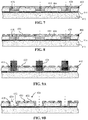
- FIGS. 5-18 are a series of diagrams illustrating steps in assembling a wafer level semiconductor device with wettable flanks in accordance with another embodiment of the present invention.
- FIG. 5A is an isometric view of the wafer 400 and FIG. 5B is a cross-sectional side view of the wafer 400 from the line B-B of FIG. 5A .
- the wafer 400 comprises a plurality of semiconductor dies 406 and has saw streets 408 located between adjacent dies. Each die 406 has one or more electrical contacts 410 formed on the top surface 402.
- each die 400 comprises one or more active components (i.e., internal circuitry not shown) such as transistors or diodes, and the electrical contacts 400 that are preferably formed by depositing a patterned metal layer on the top surface 402, provide electrical connections to the active components within the die 406.
- the bottom surface 404 of the wafer 400 is mounted on a top surface of a carrier 412 with an adhesive material 414.
- the carrier 412 is a semiconductor substrate.
- the wafer 400 is cut along the saw streets 408 with a first blade 416 to form a plurality of first trenches 418 between adjacent ones of the dies 406.
- the first blade 416 cuts down to the adhesive material 414.
- the first blade 416 cuts beyond the adhesive material 414 and into, and half-cuts, the carrier 412.
- the semiconductor dies 406 are encapsulated with a molding material 420.
- the molding material 420 covers the top surfaces 402 of the dies 406 and fills the first trenches 418.
- one or more openings 422 are formed over the top surface of each die 406 to at least partially expose the corresponding electrical contacts 410 from the molding material 420.
- the openings 422 are formed by etching or laser drilling.
- a half-cut is performed along the first trenches 418 with a second blade 424 to form a plurality of second trenches 426 respectively within the first trenches 418.
- the molding material 420 defines a package body of each semiconductor device 428, defining a top surface 430 and a side surface 432.
- a metal layer 434 is formed over the top surface 430 of each package body.
- the metal layer 434 fills the openings 422 and electrically connects the die electrical contacts 410.
- the metal layer 434 also extends to the side surface 432 of each package body and a bottom surface 436 of each of the second trenches 426.
- FIGS. 10A and 10B respectively show a cross-sectional side view and a top plan view of the wafer 400 after the metal layer 434 is formed thereover.
- the metal layer 434 is formed by sputtering or plating.
- the metal layer 434 comprises copper.
- FIGS. 11A and 11B openings 438 are selectively formed within the metal layer 434 by half-cutting to electrically isolate the electrical contacts 410 of each semiconductor die from each other.
- FIGS. 11A and 11B respectively show a cross-sectional side view and a top plan view of the wafer 400 after the openings 438 are formed in the metal layer 434.
- the molding material 420 is exposed from the openings 438.
- the openings 438 are parallel to the saw streets 408 in one direction.
- the openings 438 do not extend to the edge of the wafer 400, such that the metal layer 434 comprises one piece of metal and is not split by any of the openings 438.
- the metal layer 434 is coated with a wettable material 440 by electro-plating.
- the wettable material 440 may comprise tin.
- the electro-plating is performed before the openings 438 are formed.
- singulation is performed along the second trenches 426 with a second blade 442 to separate the semiconductor devices 428 from each other, where FIG. 13A shows the assembly being cut and FIG. 13B showing the separated devices 428.
- FIGS. 14, 15A and 15B illustrate steps that are substantially the same as the steps shown in FIGS. 12, 13A and 13B except that a coating layer 444 is formed on a bottom surface of the wafer carrier 412.
- the coating layer 444 provides mechanical and chemical protection to the backside of the semiconductor device 428.
- the coating layer 444 blocks out light.
- the coating layer 444 preferably comprises a non-conductive material such as plastic.
- FIGS. 16-18 illustrate steps performed after the step shown in FIG. 12 , in accordance with a preferred embodiment of the present invention.
- a coating layer 444 (same as the coating layer 444 of FIG. 14 ) is formed on a bottom surface of the molded package bodies of semiconductor devices 446.
- the coating layer 444 provides mechanical and chemical protection for a backside of the semiconductor devices 446, especially a backside of the semiconductor die.
- the coating layer 444 blocks out light.
- the coating layer 444 comprises a non-conductive material such as plastic.
- singulation is performed along the second trenches 426 to separate the semiconductor devices 446 from each other.
Landscapes
- Engineering & Computer Science (AREA)
- Microelectronics & Electronic Packaging (AREA)
- Physics & Mathematics (AREA)
- Structures Or Materials For Encapsulating Or Coating Semiconductor Devices Or Solid State Devices (AREA)
- Geometry (AREA)
- Dicing (AREA)
- Health & Medical Sciences (AREA)
- Electromagnetism (AREA)
- Toxicology (AREA)
- Manufacturing & Machinery (AREA)
- Encapsulation Of And Coatings For Semiconductor Or Solid State Devices (AREA)
Abstract
Description
- The present invention relates to integrated circuit (IC) device assembly and, more particularly, to a wafer level semiconductor device with wettable flanks.
- Wafer level packages (WLPs) are becoming increasingly important for applications that require a small footprint with improved electrical performance. Wafer level packages are commonly used, for instance, in mobile communications devices such as mobile telephones.
-
FIG. 1 is a cross-sectional side view of aconventional WLP 100. The WLP 100 includes a plurality ofactive pads 102 exposed on a bottom surface of theWLP 100. Theactive pads 102 are mounted tocontact elements 104, such as pads on a printed circuit board (PCB) withsolder 106. -
FIG. 2 is an enlarged schematic bottom plan view of apart 108 of theWLP 100 along line A-A ofFIG. 1 . The bottom surface of the WLP 100 includes theactive pad 102, which is a metal area, a sawscribe lane area 110 located at a peripheral area of the bottom surface of theWLP 100, which is a non-passivated area, and apassivation overlap area 112 located between theactive pad 102 and the sawscribe lane area 110. However, as shown inFIG. 2 , improper cleaning of theWLP 100, or excessive solder, together with a very narrow separation between theactive pad 102 and the sawscribe lane area 110 can result in a flux residue orsolder flake 114 may bridge theactive pad 102 and the saw scribedlane area 110, which raises the possibility of an IR leakage issue. In addition, since theactive pad 102 does not extend all the way to the side of theWLP 100, once theWLP 100 is mounted to the PCB and theactive pads 102 are soldered to thecorresponding contact elements 104, it is difficult to inspect the solder joints to determine if there are any potential solder joint defects. Accordingly, it would be advantageous to have a WLP with inspectable solder joints. - The invention, together with objects and advantages thereof, may best be understood by reference to the following description of preferred embodiments together with the accompanying drawings in which:
-
FIG. 1 is a cross-sectional side view of a conventional wafer level semiconductor device; -
FIG. 2 is an enlarged bottom plan view of the conventional wafer level semiconductor device ofFIG. 1 along line A-A ofFIG. 1 ; -
FIGS. 3A and 3B are respectively a cross-sectional side view and an isometric view of a wafer level semiconductor device with wettable flanks in accordance with an embodiment of the present invention; -
FIGS. 4A and 4B are respectively a cross-sectional side view and an isometric view of a wafer level semiconductor device with wettable flanks in accordance with another embodiment of the present invention; and -
FIGS. 5A-5B ,6A-6B, 7-8, 9A-9B, 10A-10B, 11A-11B, 12, 13A-13B, 14, 15A-15B, and 16-18 are a series of diagrams illustrating steps in assembling a wafer level semiconductor device with wettable flanks in accordance with an embodiment of the present invention. - The detailed description set forth below in connection with the appended drawings is intended as a description of presently preferred embodiments of the invention, and is not intended to represent the only forms in which the present invention may be practised. It is to be understood that the same or equivalent functions may be accomplished by different embodiments that are intended to be encompassed within the spirit and scope of the invention. In the drawings, like numerals are used to indicate like elements throughout. It also should be noted that the drawings provide enlarged views and may not be drawn to scale so that particular features of the invention may be better understood. The terms "comprises," "comprising," or any variations thereof, are intended to cover a non-exclusive inclusion, such that module, circuit, device components, structures and method steps that comprises a list of elements or steps does not include only those elements but may include other elements or steps not expressly listed or inherent to such module, circuit, device components or steps. An element or step proceeded by "comprises ... a" does not, without more constraints, preclude the existence of additional identical elements or steps that comprises the element or step.
- In one embodiment, the present invention provides a semiconductor device including a semiconductor die having a top surface that has one or more electrical contacts formed thereon, and an opposite bottom surface, and a molding material encapsulating the top surface and at least a part of a side surface of the semiconductor die. The molding material defines a package body that has a top surface and a side surface. A plurality of openings are formed on the top surface of the package body, and the plurality of electrical contacts are partially exposed from the molding material through the openings. The semiconductor device further includes a metal layer formed over and electrically connected to the electrical contacts through the openings. The metal layer extends to and at least partially covers the side surface of the package body. In another embodiment, the present invention provides a method for packaging a semiconductor device. The method includes providing a wafer that has a top surface and an opposite bottom surface. The wafer includes a plurality of semiconductor dies and saw streets located between adjacent dies. Each semiconductor die has a plurality of electrical contacts formed on the top surface. The method also includes cutting the wafer along the saw streets to form a plurality of first trenches between adjacent semiconductor dies, and then encapsulating the semiconductor dies with a molding material. The molding material covers the top surfaces of the semiconductor dies and fills the first trenches. Openings are formed to at least partially expose the electrical contacts from the molding material. The method further includes cutting the first trenches to form a plurality of second trenches. The molding material defines a package body of each semiconductor device, such that each device has a top surface and a side surface. The method further includes forming a metal layer over the top surface of each package body. The metal layer fills the openings and electrically connects the electrical contacts. The metal layer also extends to the side surface of each package body and to a bottom surface of each second trench. The method includes selectively cutting the metal layer to electrically isolate the electrical contacts of each semiconductor die, and cutting the second trenches to singulate the semiconductor devices from each other.
- Referring now to
FIGS. 3A and 3B , an example of a waferlevel semiconductor device 200 with wettable flanks in accordance with an embodiment of the present invention is shown. In particular,FIG. 3A shows a cross-sectional side view of the waferlevel semiconductor device 200, andFIG. 3B shows an isometric view of thedevice 200. Thedevice 200 includes asemiconductor die 202 having atop surface 204 that has one or moreelectrical contacts 206 formed thereon, and anopposite bottom surface 208. In a preferred embodiment, thesemiconductor die 202 comprises one or more active components (not shown) such as transistors or diodes, and the one or moreelectrical contacts 206. The electrical contacts preferably are formed by depositing a patterned metal layer on the dietop surface 204, and provide electrical connections to the one or more active components within thesemiconductor die 202. - The
semiconductor device 200 also includes amolding material 210 that covers thetop surface 204 and at least a part of a side surface of thesemiconductor die 202. Themolding material 210 defines a package body that has atop surface 212 and aside surface 214. One ormore openings 216 are formed in thetop surface 212 of the package body such that theelectrical contacts 206 are at least partially exposed from themolding material 210 through theopenings 216. Thedevice 200 further includes ametal layer 218 formed over and electrically connected to theelectrical contacts 206 through theopenings 216. Themetal layer 218 extends to and at least partially covers theside surface 214 of the package body. Themetal layers 218, which are respectively electrically connected to theelectrical contacts 206, are spaced and isolated from each other by agap 220 located therebetween. Themetal layers 218 form mounting pads of thesemiconductor device 200. In a preferred embodiment, themetal layer 218 comprises copper.In another preferred embodiment, themetal layer 218 is coated with awettable material 222, such as tin, by a plating process, such that thedevice 200 has wettable flanks that allow for solder joint inspection. - In a preferred embodiment, the
device 200 includes a diecarrier 224. Thebottom surface 208 of thedie 202 is mounted to a top surface of thedie carrier 224 with anadhesive material 226. Thedie carrier 224 is preferably a semiconductor substrate. In a preferred embodiment, themolding material 210 further covers aperipheral area 228 of the top surface of thedie carrier 224 that is not covered by the semiconductor die 202, and themetal layer 218 extends over themolding material 210 that covers theperipheral area 228. - Referring now to
FIGS. 4A and 4B , an example of a waferlevel semiconductor device 300 with wettable flanks in accordance with another embodiment of the present invention is shown. Thedevice 300 is substantially the same as thedevice 200 except that thedevice 300 further comprises acoating layer 302 formed on a bottom surface of thedie carrier 224. Thecoating layer 302 provides mechanical and chemical protection to the back or bottom side of thedevice 300. In a preferred embodiment, thecoating layer 302 blocks light. Thecoating layer 302 may comprise a non-conductive material such as plastic. -
FIGS. 5-18 are a series of diagrams illustrating steps in assembling a wafer level semiconductor device with wettable flanks in accordance with another embodiment of the present invention. - Starting with
FIGS. 5A and 5B , awafer 400 that has atop surface 402 and an oppositebottom surface 404 is provided.FIG. 5A is an isometric view of thewafer 400 andFIG. 5B is a cross-sectional side view of thewafer 400 from the line B-B ofFIG. 5A . Thewafer 400 comprises a plurality of semiconductor dies 406 and has sawstreets 408 located between adjacent dies. Each die 406 has one or moreelectrical contacts 410 formed on thetop surface 402. In a preferred embodiment, each die 400 comprises one or more active components (i.e., internal circuitry not shown) such as transistors or diodes, and theelectrical contacts 400 that are preferably formed by depositing a patterned metal layer on thetop surface 402, provide electrical connections to the active components within thedie 406. In a preferred embodiment, thebottom surface 404 of thewafer 400 is mounted on a top surface of acarrier 412 with anadhesive material 414. In a preferred embodiment, thecarrier 412 is a semiconductor substrate. - In the next step illustrated in
FIGS. 6A and 6B , thewafer 400 is cut along thesaw streets 408 with afirst blade 416 to form a plurality offirst trenches 418 between adjacent ones of the dies 406. In a preferred embodiment, thefirst blade 416 cuts down to theadhesive material 414. In another preferred embodiment, thefirst blade 416 cuts beyond theadhesive material 414 and into, and half-cuts, thecarrier 412. - In the next step illustrated in
FIG. 7 , the semiconductor dies 406 are encapsulated with amolding material 420. Themolding material 420 covers thetop surfaces 402 of the dies 406 and fills thefirst trenches 418. Then inFIG. 8 , one ormore openings 422 are formed over the top surface of each die 406 to at least partially expose the correspondingelectrical contacts 410 from themolding material 420. In a preferred embodiment, theopenings 422 are formed by etching or laser drilling. - In the next step illustrated in
FIGS. 9A and 9B , a half-cut is performed along thefirst trenches 418 with asecond blade 424 to form a plurality ofsecond trenches 426 respectively within thefirst trenches 418. After the half-cut, themolding material 420 defines a package body of eachsemiconductor device 428, defining atop surface 430 and aside surface 432. - In the next step illustrated in
FIGS. 10A and 10B , ametal layer 434 is formed over thetop surface 430 of each package body. Themetal layer 434 fills theopenings 422 and electrically connects the dieelectrical contacts 410. Themetal layer 434 also extends to theside surface 432 of each package body and abottom surface 436 of each of thesecond trenches 426. -
FIGS. 10A and 10B respectively show a cross-sectional side view and a top plan view of thewafer 400 after themetal layer 434 is formed thereover. In a preferred embodiment, themetal layer 434 is formed by sputtering or plating. In one embodiment, themetal layer 434 comprises copper. - Then in
FIGS. 11A and 11B ,openings 438 are selectively formed within themetal layer 434 by half-cutting to electrically isolate theelectrical contacts 410 of each semiconductor die from each other.FIGS. 11A and 11B respectively show a cross-sectional side view and a top plan view of thewafer 400 after theopenings 438 are formed in themetal layer 434. Themolding material 420 is exposed from theopenings 438. In a preferred embodiment, theopenings 438 are parallel to thesaw streets 408 in one direction. In another preferred embodiment, theopenings 438 do not extend to the edge of thewafer 400, such that themetal layer 434 comprises one piece of metal and is not split by any of theopenings 438. In a preferred embodiment, as shown inFIG. 12 , themetal layer 434 is coated with awettable material 440 by electro-plating. Thewettable material 440 may comprise tin. In an alternate embodiment, the electro-plating is performed before theopenings 438 are formed. - In the next step illustrated in
FIGS. 13A and 13B , singulation is performed along thesecond trenches 426 with asecond blade 442 to separate thesemiconductor devices 428 from each other, whereFIG. 13A shows the assembly being cut andFIG. 13B showing the separateddevices 428. -
FIGS. 14, 15A and 15B illustrate steps that are substantially the same as the steps shown inFIGS. 12, 13A and 13B except that acoating layer 444 is formed on a bottom surface of thewafer carrier 412. Thecoating layer 444 provides mechanical and chemical protection to the backside of thesemiconductor device 428. In a preferred embodiment, thecoating layer 444 blocks out light.Thecoating layer 444 preferably comprises a non-conductive material such as plastic. -
FIGS. 16-18 illustrate steps performed after the step shown inFIG. 12 , in accordance with a preferred embodiment of the present invention. - In the step illustrated in
FIG. 16 , thewafer carrier 412 shown inFIG. 12 is removed. Then in the step shown inFIG. 17 , a coating layer 444 (same as thecoating layer 444 ofFIG. 14 ) is formed on a bottom surface of the molded package bodies ofsemiconductor devices 446. Thecoating layer 444 provides mechanical and chemical protection for a backside of thesemiconductor devices 446, especially a backside of the semiconductor die. In a preferred embodiment, thecoating layer 444 blocks out light. In a preferred embodiment, thecoating layer 444 comprises a non-conductive material such as plastic. InFIG. 18 , singulation is performed along thesecond trenches 426 to separate thesemiconductor devices 446 from each other. - The description of the preferred embodiments of the present invention has been presented for purposes of illustration and description, but is not intended to be exhaustive or to limit the invention to the forms disclosed. It will be appreciated by those skilled in the art that changes could be made to the embodiments described above without departing from the broad inventive concept thereof. It is understood, therefore, that this invention is not limited to the particular embodiment disclosed, but covers modifications within the spirit and scope of the present invention as defined by the appended claims.
Claims (15)
- A semiconductor device, comprising:a semiconductor die having a top surface that has one or more electrical contacts formed thereon, and an opposite bottom surface;a molding material encapsulating the top surface and at least a part of a side surface of the semiconductor die, wherein the molding material defines a package body that has a top surface and a side surface;a plurality of openings formed on the top surface of the package body, wherein the plurality of electrical contacts are partially exposed from the molding material through the openings; anda metal layer formed over and electrically connected to the electrical contacts through the openings, wherein the metal layer extends to and at least partially covers the side surface of the package body.
- The semiconductor device of claim 1, wherein the metal layer is coated with a wettable material by electrically conductive plating.
- The semiconductor device of claim 1, wherein the metal layer comprises copper.
- The semiconductor device of claim 1, further comprising a layer of non-conductive material coated on a bottom surface of the package body.
- The semiconductor device of claim 1, further comprising a die carrier, wherein the bottom surface of the semiconductor die is mounted to a top surface of the die carrier.
- The semiconductor device of claim 5, further comprising an adhesive material that attaches the bottom surface of the semiconductor die to the top surface of the die carrier.
- The semiconductor device of claim 5, wherein the molding material encapsulates a peripheral area of the top surface of the die carrier that is not covered by the semiconductor die.
- The semiconductor device of claim 7, wherein the metal layer extends from the side surface of the package body to the peripheral area of the top surface of the die carrier.
- The semiconductor device of claim 5, further comprising a layer of non-conductive material coated on a bottom surface of the die carrier.
- A method for assembling a semiconductor device, the method comprising:providing a wafer that has a top surface and an opposite bottom surface, wherein the wafer comprises a plurality of semiconductor dies and saw streets located between adjacent ones of the dies, wherein each die has a plurality of electrical contacts formed on the top surface;cutting the wafer along the saw streets to form a plurality of first trenches between adjacent ones of the dies;encapsulating the dies with a molding material, wherein the molding material covers top surfaces of the dies and fills the first trenches;forming openings to at least partially expose the electrical contacts from the molding material;cutting the plurality of first trenches to form a plurality of second trenches, wherein the molding material defines a package body of each semiconductor device that has a top surface and a side surface;forming a metal layer over the top surface of each package body, wherein the metal layer fills the openings to electrically connect the electrical contacts, and extends to the side surface of each package body and a bottom surface of each second trench;selectively cutting the metal layer to electrically isolate the electrical contacts of each die from each other;cutting in the second trenches to singulate the semiconductor devices from each other.
- The method of claim 10, further comprising mounting the bottom surface of the wafer to a top surface of a wafer carrier, wherein the bottom surface of the wafer is mounted to the top surface of the wafer carrier with an adhesive material.
- The method of claim 10, wherein the metal layer comprises copper.
- The method of claim 10, wherein the metal layer is formed by sputtering or plating.
- The method of claim 10, further comprising coating the metal layer with a wettable material by electro-plating.
- The method of claim 10, further comprising forming a non-conductive coating layer on a bottom surface of the semiconductor device, wherein the non-conductive coating layer comprises a light-blocking plastic material.
Applications Claiming Priority (1)
| Application Number | Priority Date | Filing Date | Title |
|---|---|---|---|
| US15/259,063 US10410941B2 (en) | 2016-09-08 | 2016-09-08 | Wafer level semiconductor device with wettable flanks |
Publications (1)
| Publication Number | Publication Date |
|---|---|
| EP3293760A1 true EP3293760A1 (en) | 2018-03-14 |
Family
ID=59258022
Family Applications (1)
| Application Number | Title | Priority Date | Filing Date |
|---|---|---|---|
| EP17178522.3A Pending EP3293760A1 (en) | 2016-09-08 | 2017-06-28 | Wafer level semiconductor device with wettable flanks |
Country Status (3)
| Country | Link |
|---|---|
| US (1) | US10410941B2 (en) |
| EP (1) | EP3293760A1 (en) |
| CN (2) | CN117133750A (en) |
Cited By (6)
| Publication number | Priority date | Publication date | Assignee | Title |
|---|---|---|---|---|
| US11393699B2 (en) | 2019-12-24 | 2022-07-19 | Vishay General Semiconductor, Llc | Packaging process for plating with selective molding |
| US11450534B2 (en) | 2019-12-24 | 2022-09-20 | Vishay General Semiconductor, Llc | Packaging process for side-wall plating with a conductive film |
| US12211704B2 (en) | 2019-03-08 | 2025-01-28 | Siliconix Incorporated | Semiconductor package having side wall plating |
| US12224232B2 (en) | 2019-03-08 | 2025-02-11 | Siliconix Incorporated | Semiconductor package having side wall plating |
| FR3155948A1 (en) * | 2023-11-23 | 2025-05-30 | Stmicroelectronics International N.V. | Manufacturing process for wettable edge electronic components |
| EP4567869A1 (en) * | 2023-12-08 | 2025-06-11 | STMicroelectronics International N.V. | Method for manufacturing electronic components |
Families Citing this family (8)
| Publication number | Priority date | Publication date | Assignee | Title |
|---|---|---|---|---|
| US10818711B2 (en) * | 2017-04-24 | 2020-10-27 | California Institute Of Technology | Narrowband light filters |
| DE102018132447B4 (en) * | 2018-12-17 | 2022-10-13 | Infineon Technologies Ag | Semiconductor device and method of manufacturing a semiconductor device |
| US11121105B2 (en) * | 2019-07-06 | 2021-09-14 | Amkor Technology Singapore Holding Pte. Ltd. | Semiconductor devices and methods of manufacturing semiconductor devices |
| FR3104315B1 (en) | 2019-12-04 | 2021-12-17 | St Microelectronics Tours Sas | Electronic chip manufacturing process |
| FR3104317A1 (en) * | 2019-12-04 | 2021-06-11 | Stmicroelectronics (Tours) Sas | Electronic chip manufacturing process |
| CN110943041A (en) * | 2019-12-16 | 2020-03-31 | 山东砚鼎电子科技有限公司 | Semiconductor structure with side surface led out, manufacturing method thereof and stacking structure |
| FR3123148A1 (en) * | 2021-05-18 | 2022-11-25 | Stmicroelectronics (Tours) Sas | Manufacture of electronic chips |
| FR3126540A1 (en) | 2021-08-31 | 2023-03-03 | Stmicroelectronics (Tours) Sas | Process for manufacturing electronic chips |
Citations (5)
| Publication number | Priority date | Publication date | Assignee | Title |
|---|---|---|---|---|
| US6285085B1 (en) * | 1997-08-13 | 2001-09-04 | Citizen Watch Co., Ltd. | Semiconductor device, method of fabricating the same and structure for mounting the same |
| US20050121795A1 (en) * | 2003-10-31 | 2005-06-09 | Infineon Technologies Ag | Semiconductor component and corresponding fabrication/mounting method |
| US20090026591A1 (en) * | 2007-07-27 | 2009-01-29 | Seung Hyun Lee | Semiconductor package adapted for high-speed data processing and damage prevention of chips packaged therein and method for fabricating the same |
| US20090266593A1 (en) * | 2008-04-24 | 2009-10-29 | Vishay Semiconductor Gmbh | Surface-mountable electronic device |
| US20110018116A1 (en) * | 2009-07-22 | 2011-01-27 | Alpha And Omega Semiconductor Incorporated | Chip scale surface mounted semiconductor device package and process of manufacture |
Family Cites Families (8)
| Publication number | Priority date | Publication date | Assignee | Title |
|---|---|---|---|---|
| DE10202881B4 (en) | 2002-01-25 | 2007-09-20 | Infineon Technologies Ag | Method for producing semiconductor chips with a chip edge protection layer, in particular for wafer level packaging chips |
| JP2006339365A (en) * | 2005-06-01 | 2006-12-14 | Mitsui Mining & Smelting Co Ltd | WIRING BOARD AND ITS MANUFACTURING METHOD, MULTILAYER LAMINATED WIRING BOARD MANUFACTURING METHOD, AND VIA HOLE FORMING METHOD |
| US8927339B2 (en) * | 2010-11-22 | 2015-01-06 | Bridge Semiconductor Corporation | Method of making thermally enhanced semiconductor assembly with bump/base/flange heat spreader and build-up circuitry |
| CN102593018B (en) * | 2011-01-11 | 2016-04-20 | 王琮淇 | Wafer-level semiconductor chip packaging method and semiconductor chip package |
| WO2012126379A1 (en) * | 2011-03-23 | 2012-09-27 | Nantong Fujitsu Microelectronics Co., Ltd. | Three-dimensional system-level packaging methods and structures |
| US8853003B2 (en) * | 2011-08-09 | 2014-10-07 | Alpha & Omega Semiconductor, Inc. | Wafer level chip scale package with thick bottom metal exposed and preparation method thereof |
| US9892952B2 (en) | 2014-07-25 | 2018-02-13 | Semiconductor Components Industries, Llc | Wafer level flat no-lead semiconductor packages and methods of manufacture |
| US9646950B2 (en) * | 2014-12-18 | 2017-05-09 | Texas Instruments Incorporated | Corrosion-resistant copper bonds to aluminum |
-
2016
- 2016-09-08 US US15/259,063 patent/US10410941B2/en active Active
-
2017
- 2017-06-28 EP EP17178522.3A patent/EP3293760A1/en active Pending
- 2017-09-08 CN CN202311212788.8A patent/CN117133750A/en active Pending
- 2017-09-08 CN CN201710806591.5A patent/CN107808871A/en active Pending
Patent Citations (5)
| Publication number | Priority date | Publication date | Assignee | Title |
|---|---|---|---|---|
| US6285085B1 (en) * | 1997-08-13 | 2001-09-04 | Citizen Watch Co., Ltd. | Semiconductor device, method of fabricating the same and structure for mounting the same |
| US20050121795A1 (en) * | 2003-10-31 | 2005-06-09 | Infineon Technologies Ag | Semiconductor component and corresponding fabrication/mounting method |
| US20090026591A1 (en) * | 2007-07-27 | 2009-01-29 | Seung Hyun Lee | Semiconductor package adapted for high-speed data processing and damage prevention of chips packaged therein and method for fabricating the same |
| US20090266593A1 (en) * | 2008-04-24 | 2009-10-29 | Vishay Semiconductor Gmbh | Surface-mountable electronic device |
| US20110018116A1 (en) * | 2009-07-22 | 2011-01-27 | Alpha And Omega Semiconductor Incorporated | Chip scale surface mounted semiconductor device package and process of manufacture |
Cited By (10)
| Publication number | Priority date | Publication date | Assignee | Title |
|---|---|---|---|---|
| US12211704B2 (en) | 2019-03-08 | 2025-01-28 | Siliconix Incorporated | Semiconductor package having side wall plating |
| US12224232B2 (en) | 2019-03-08 | 2025-02-11 | Siliconix Incorporated | Semiconductor package having side wall plating |
| US11393699B2 (en) | 2019-12-24 | 2022-07-19 | Vishay General Semiconductor, Llc | Packaging process for plating with selective molding |
| US11450534B2 (en) | 2019-12-24 | 2022-09-20 | Vishay General Semiconductor, Llc | Packaging process for side-wall plating with a conductive film |
| US11764075B2 (en) | 2019-12-24 | 2023-09-19 | Vishay General Semiconductor, Llc | Package assembly for plating with selective molding |
| US11876003B2 (en) | 2019-12-24 | 2024-01-16 | Vishay General Semiconductor, Llc | Semiconductor package and packaging process for side-wall plating with a conductive film |
| FR3155948A1 (en) * | 2023-11-23 | 2025-05-30 | Stmicroelectronics International N.V. | Manufacturing process for wettable edge electronic components |
| EP4571825A1 (en) * | 2023-11-23 | 2025-06-18 | STMicroelectronics International N.V. | Method for producing electronic components with wettable flanks |
| EP4567869A1 (en) * | 2023-12-08 | 2025-06-11 | STMicroelectronics International N.V. | Method for manufacturing electronic components |
| FR3156587A1 (en) * | 2023-12-08 | 2025-06-13 | Stmicroelectronics International N.V. | Electronic component manufacturing process |
Also Published As
| Publication number | Publication date |
|---|---|
| US10410941B2 (en) | 2019-09-10 |
| CN107808871A (en) | 2018-03-16 |
| CN117133750A (en) | 2023-11-28 |
| US20180068920A1 (en) | 2018-03-08 |
Similar Documents
| Publication | Publication Date | Title |
|---|---|---|
| US10410941B2 (en) | Wafer level semiconductor device with wettable flanks | |
| TWI569398B (en) | Semiconductor component package and manufacturing method thereof | |
| KR101655897B1 (en) | A microelectronic assembly and a method of fabricating a stacked microelectronic assembly | |
| CN1320617C (en) | Semiconductor device chip scale surface assembling and packaging, and mfg. method therefor | |
| KR100917745B1 (en) | Semiconductor device and manufacturing method thereof | |
| CN102214623B (en) | Chip package and method for forming the same | |
| US8673690B2 (en) | Method for manufacturing a semiconductor device and a semiconductor device | |
| US7772698B2 (en) | Package structure for integrated circuit device | |
| TW201523825A (en) | Semiconductor device and method of manufacturing same | |
| EP3306660A2 (en) | Leadframe-less surface mount semiconductor device | |
| US8614488B2 (en) | Chip package and method for forming the same | |
| CN101290892A (en) | Sensing type semiconductor device and manufacturing method thereof | |
| US20080197438A1 (en) | Sensor semiconductor device and manufacturing method thereof | |
| CN110223925A (en) | The method of manufacturing semiconductor devices | |
| US9318461B2 (en) | Wafer level array of chips and method thereof | |
| US7443043B2 (en) | Circuit device and method of manufacture thereof | |
| US11094562B2 (en) | Semiconductor device and method of manufacture | |
| US10916485B2 (en) | Molded wafer level packaging | |
| CN100353532C (en) | Semiconductor device | |
| TW201705439A (en) | Semiconductor device | |
| US7696615B2 (en) | Semiconductor device having pillar-shaped terminal | |
| US10930615B2 (en) | Semiconductor device and method of manufacturing semiconductor device | |
| CN102263076A (en) | Package structure and method for forming package structure | |
| US20240413067A1 (en) | Electronic package module and method for fabrication of the same | |
| CN120977880A (en) | Method for manufacturing electronic components with wettable winglets |
Legal Events
| Date | Code | Title | Description |
|---|---|---|---|
| PUAI | Public reference made under article 153(3) epc to a published international application that has entered the european phase |
Free format text: ORIGINAL CODE: 0009012 |
|
| STAA | Information on the status of an ep patent application or granted ep patent |
Free format text: STATUS: THE APPLICATION HAS BEEN PUBLISHED |
|
| AK | Designated contracting states |
Kind code of ref document: A1 Designated state(s): AL AT BE BG CH CY CZ DE DK EE ES FI FR GB GR HR HU IE IS IT LI LT LU LV MC MK MT NL NO PL PT RO RS SE SI SK SM TR |
|
| AX | Request for extension of the european patent |
Extension state: BA ME |
|
| STAA | Information on the status of an ep patent application or granted ep patent |
Free format text: STATUS: REQUEST FOR EXAMINATION WAS MADE |
|
| 17P | Request for examination filed |
Effective date: 20180904 |
|
| RBV | Designated contracting states (corrected) |
Designated state(s): AL AT BE BG CH CY CZ DE DK EE ES FI FR GB GR HR HU IE IS IT LI LT LU LV MC MK MT NL NO PL PT RO RS SE SI SK SM TR |
|
| STAA | Information on the status of an ep patent application or granted ep patent |
Free format text: STATUS: EXAMINATION IS IN PROGRESS |
|
| 17Q | First examination report despatched |
Effective date: 20210610 |