EP3293519B1 - A physiological parameter measurement module - Google Patents
A physiological parameter measurement module Download PDFInfo
- Publication number
- EP3293519B1 EP3293519B1 EP17190413.9A EP17190413A EP3293519B1 EP 3293519 B1 EP3293519 B1 EP 3293519B1 EP 17190413 A EP17190413 A EP 17190413A EP 3293519 B1 EP3293519 B1 EP 3293519B1
- Authority
- EP
- European Patent Office
- Prior art keywords
- test strip
- strip reader
- main body
- module main
- conductive element
- Prior art date
- Legal status (The legal status is an assumption and is not a legal conclusion. Google has not performed a legal analysis and makes no representation as to the accuracy of the status listed.)
- Active
Links
Images




Classifications
-
- G—PHYSICS
- G01—MEASURING; TESTING
- G01N—INVESTIGATING OR ANALYSING MATERIALS BY DETERMINING THEIR CHEMICAL OR PHYSICAL PROPERTIES
- G01N33/00—Investigating or analysing materials by specific methods not covered by groups G01N1/00 - G01N31/00
- G01N33/48—Biological material, e.g. blood, urine; Haemocytometers
- G01N33/483—Physical analysis of biological material
- G01N33/487—Physical analysis of biological material of liquid biological material
- G01N33/49—Blood
-
- G—PHYSICS
- G01—MEASURING; TESTING
- G01N—INVESTIGATING OR ANALYSING MATERIALS BY DETERMINING THEIR CHEMICAL OR PHYSICAL PROPERTIES
- G01N27/00—Investigating or analysing materials by the use of electric, electrochemical, or magnetic means
- G01N27/02—Investigating or analysing materials by the use of electric, electrochemical, or magnetic means by investigating impedance
- G01N27/04—Investigating or analysing materials by the use of electric, electrochemical, or magnetic means by investigating impedance by investigating resistance
-
- G—PHYSICS
- G01—MEASURING; TESTING
- G01N—INVESTIGATING OR ANALYSING MATERIALS BY DETERMINING THEIR CHEMICAL OR PHYSICAL PROPERTIES
- G01N33/00—Investigating or analysing materials by specific methods not covered by groups G01N1/00 - G01N31/00
- G01N33/48—Biological material, e.g. blood, urine; Haemocytometers
- G01N33/483—Physical analysis of biological material
- G01N33/487—Physical analysis of biological material of liquid biological material
- G01N33/4875—Details of handling test elements, e.g. dispensing or storage, not specific to a particular test method
- G01N33/48771—Coding of information, e.g. calibration data, lot number
-
- G—PHYSICS
- G01—MEASURING; TESTING
- G01N—INVESTIGATING OR ANALYSING MATERIALS BY DETERMINING THEIR CHEMICAL OR PHYSICAL PROPERTIES
- G01N33/00—Investigating or analysing materials by specific methods not covered by groups G01N1/00 - G01N31/00
- G01N33/48—Biological material, e.g. blood, urine; Haemocytometers
- G01N33/483—Physical analysis of biological material
- G01N33/487—Physical analysis of biological material of liquid biological material
- G01N33/48785—Electrical and electronic details of measuring devices for physical analysis of liquid biological material not specific to a particular test method, e.g. user interface or power supply
Definitions
- the present invention is related to a test strip reader, and more particularly to a test strip reader disposed in an electronic device for measuring an analyte.
- Devices for measuring physiological parameters can obtain samples through test strips after sample collecting to facilitate the measurement under predetermined test conditions.
- Some analyte measuring devices can read different types of test strips such as the one disclosed in German Patent Application DE 10 2008 029715 A1 , which includes a retainer for receiving a sample strip.
- the analyte measuring device In order for the analyte measuring device to be able to identify the type of test strips or to enable anti-counterfeiting, one may mechanically encode the test strip at a certain portion of the test strip, for example by making some coding recesses.
- the analyte measurement device can be used to read the test strip, and at the same time can also be used for the identification of these recesses to identify the type of test strips to assist the reading module to select the appropriate test configuration as well as enable the anti-counterfeiting function.
- Fig. 1 is a schematic diagram showing an upper cover 101 having a top structure 104 of a strip slot before assembly according to a prior art design.
- the space for the strip slot is formed after the circuit board 103 having a strip reader module 100 has been assembled with the upper cover 101 and a back cover 102 piece by piece.
- the distance between the strip contacting surfaces of the strip slot varies due to the tolerances control of the upper cover 101 and the strip reader module 100 disposed on the circuit board 103 during manufacturing.
- Eventually a reworking for adjusting the space for the strip slot is inevitable when the space is out of specification or the strip reader module 100 cannot precisely identify the code on the strip due to measurement bias.
- contamination often occurs when the reader module receives a test strip containing a blood sample. If the blood sample accidentally enters the device for measuring physiological parameters, it may cause inspection errors due to contamination or even malfunctions of electronic components. Thus, there is also a need to avoid potential contamination.
- test strip reader disposed in an electronic device for measuring an analyte
- test strip reader according to independent claim 1 J Z is disclosed.
- the novel design in the present invention can fully satisfy the requirements in terms of controlling the manufacturing tolerance of the strip slot as well as contamination prevention and ease of assembly.
- the present invention has utility for industry.
- the test strip reader module 200 comprises a circuit board 280 and a module main body 240 disposed thereon.
- the module main body 240 includes an upper cover 245, and a strip insertion slot 210 is formed between the module main body 240 and the upper cover 245.
- the module main body 240 also includes two electrical contact portions 243 disposed at the location of the strip insertion slot 210.
- the two electrical contact portions 243 can be electrically connected to corresponding electrodes (not shown) on a test strip 120 when inserted into the strip insertion slot 210.
- Materials for the electrical contact portions 243 and the corresponding electrodes are preferably of gold material such as the material used by Rightest® blood test strip accompanied with an embedded gold electrode technology (for example, the Validus® technology) to have better stability and conductivity.
- the test strip reader module 200 comprises the module main body 240 including the upper cover 245. As shown in Fig. 2B , the module main body 240 and the upper cover 245 are formed integrally. An upper strip contacting surface 212 and a lower strip contacting surface 214 can be defined in the strip insertion slot 210.
- a height H1 of the strip insertion slot 210 for accommodating the test strip 120 is defined by the upper strip contacting surface 212 and the lower strip contacting surface 214 which makes the height of strip insertion slot 210 can be controlled by a single element since the height is defined when the module main body 240 was formed.
- the height H1 of the strip insertion slot 210 can be defined as a standard thickness of the test strip 120 plus a tolerance ranging between 0.05 and 0.5 millimeters.
- the height H1 ranges between 1.05 and 1.5 millimeters when the standard thickness of the test strip 120 is 1 millimeter.
- the module main body 240 also includes a first operation movement assembly 255 having an actuating element 250 for contacting a coding recess 122 on the test strip 120 and a blocking element 260 disposed below the actuating element 250, and a second operation movement assembly 275 having a conductive element 270 disposed under the blocking element 260 and an elastic element 220 for pushing the conductive element 270 upward. It is appreciated that a set of the first and the second operation movement assemblies 255, 275 are contained in one of operation holes 242 of the module main body 240. Alternatively, in other embodiments, the first operation movement assembly 255 is disposed in one operation hole 242 while the second operation movement assembly 275 is accommodated in a supporting portion 295 of the module main body 240.
- the elastic element 220 can be, but not limited to, a spring, a metal elastic sheet or a metal dome.
- the shape of the conductive element 270 can be, but is not limited to, a column or ball-like element.
- the material of the conductive element 270 can be a metal material such as steel.
- the blocking element 260 is made of an elastic material such as rubber or silicone.
- a grounding element 290 is disposed under the blocking element 260, and the circuit board 280 has a signal source 282 providing an electronic signal Vs.
- Vs electronic signal
- the conductive element 270 contacts the grounding element 290 due to a push from the elastic element 220, and a conducting condition is formed when the conductive element 270 is in contact with the grounding element 290 so the electronic signal Vs from the signal source 282 can come all the way through a circuit via the conductive element 270 to the grounding element 290.
- a current may exist in the circuit if the electronic signal is a voltage.
- the actuating element 250 is not pushed down if the actuating element 250 is located under the corresponding coding recess 122 without a protrusion portion 124. Consequently, the conducting condition occurs, which can be determined as a first encoding signal or a first read signal.
- a height H2 of the protrusion portion 124 for pressing the actuation element 250 ranges between 0.4 and 0.8 millimeters. Consequently, a non-conducting condition is formed when the conductive element 270 is separated from the grounding element 290 and the electronic signal Vs from the signal source 282 cannot be transmitted to the grounding element 290, which can be determined as a second encoding signal or a second read signal.
- the read signal for a coding recess 122 at the corresponding position of the operation hole 242 can be determined based on one of the conducting and the non-conducting conditions.
- One may decode or identify the coding of a single recess 122 on the test strip 120 based on whether the current is formed due to the electronic signal Vs from the signal source 282 in the circuit board 280. For instance in a binary coding system, one of the coding conditions can be zero while the other can be one, and vice versa.
- FIG. 2D shows a sectional view of the test strip reader module according to another embodiment of the present invention.
- the operating concept for decoding the coding recesses 122 on the test strips 120 in Fig. 2D is similar to that of the embodiments illustrated in Figs. 2B and 2C , and the difference is that each of the blocking elements 260 disposed in the operation holes 242 is operated independently. Deformation of a single blocking element 260 due to the vertical movement of the corresponding actuating element 250 in response to the coding in the coding recesses 122 will not cause any influence on the movement of the blocking elements 260 in different operation holes 242, so the issue of misreading due to the influence of the movement of adjacent actuating elements 250 may never exist.
- a protrusion 268 is formed in the blocking element 260 at a location corresponding to the actuating element 250, and may have a shape to match that of the actuating element 250, so additional pressure from the actuating element 250 toward the blocking element 260 is needed for allowing the actuating element 250 moving downward.
- the portion of the conductive element 270 facing the blocking element 260 is flat. Consequently, the movement of conductive element 270 due to the compression of the blocking element 260 becomes more precise, and thus the judgment for the reading signal will be more accurate.
- the blocking element 260 includes a first blocker 262 having a cantilever shape and a second blocker 264 connected to the first blocker 262, and renders each of the actuating elements 250 disposed thereon can be moved independently without being effected by the movement in other operation holes 242 and causing a misread.
- first block 262 will deform when the blocking element 260 is compressed by the actuating element 250, and thus additional pressure from the actuating element 250 will be needed for pushing the conductive element 270 downward to achieve more accurate code reading.
- contamination such as a particle (not shown) can be collected into an L-shaped contamination collection portion 266 without effecting the electrical function down below when the contamination material accidently enters the test strip reader module 200 via the operation holes 242.
- FIG. 3 shows a sectional view of the test strip reader module 300 when the test strip 120 is inserted into the strip insertion slot 210 according to another embodiment of the present invention, wherein the disposition of the elements such as the test strip 120, circuit board 280, the upper cover 345 and the main module body 340 are similar to those in the descriptions set forth above, and the differences are in that the actuating element is replaced by an elongated conductive element 350 having a first end 352 for contacting the coding recesses 122, a second end 354 for contacting the elastic element 220, a side groove 356 having a first groove wall 357 near the first end 352 and a second groove wall 358 disposed opposite to the first groove wall 357.
- the actuating element is replaced by an elongated conductive element 350 having a first end 352 for contacting the coding recesses 122, a second end 354 for contacting the elastic element 220, a side groove 356 having a first groove wall 357 near the first end 352 and
- the second end 354 and elastic element 220 are contained in the supporting portion 395.
- the conductive element 350 at the left side faces the corresponding coding recess 122 without a protrusion, so the conductive element 350 at the left side is not compressed and the second groove wall 358 contacts the grounding element 390 to form a conducting status which can be identified as a first encoding signal
- the conductive element 350 at the right side faces to the corresponding coding recess 122 with a protrusion 124, so the conductive element 350 at the right side is compressed and moves downward and forms a separation status with the grounding element 390 which can be identified as a second encoding signal since the electronic signal Vs from the signal source 282 in the circuit board 280 cannot be transmitted to the grounding element 390 to generate a current.
- the blocking element 360 is preferably made of elastic material so it can be deformed along the vertical movement of the conductive element 350 while keeping a match condition with the first groove wall 357.
- the signal source 282 can include an ESD protection circuit for preventing the influence of electrostatic discharge caused by movement of the conductive element 350.
- the blocking elements may result in elastic fatigue and cause the test strip reader module operate abnormally.
- the present invention also provides solutions for avoiding the issue of contamination entering the inside of the reader module as described below.
- the actuating element in Figs. 2B-2D is replaced by the conductive element 350 having a cylinder-like shape while the operation holes 342 are sleeve-shaped, each of which contains one conductive element 350.
- the blocking element 360 includes a first side wall 362 matching the first groove wall 357 of the conductive element 350 and deforming along with the vertical movement of the conductive element 350. Therefore, the conductive element 350 can operate independently without being affected by the other conductive elements 350 in different operation holes 342.
- a contamination collecting device 366 is formed between the first side wall 362 and a second side wall 364, as illustrated in Fig. 3 .
- the contamination P When a contamination P such as overflow sample, quality control fluid, ash or particles accidentally enters the test strip reader module 300 from the operation holes 342, the contamination P will be contained in the contamination collecting device 366 without falling into the lower portion of the module main body 340 and affecting the electrical function thereof. It can be appreciated by the skilled person in the art based on Fig. 3 that the contamination collecting device 366 has a shape of a groove surrounding the side groove 356 of the conductive element 350.
- Fig. 4 shows how the test strip reader module 200/300 according to the present invention is assembled into an electronic device.
- the test strip reader module 200 itself has comprehensive functions for reading test strips, and can be connected to a communication module (not shown) disposed on a variety of mobile electronic devices such as cell phones, PDA or wearable electronic devices to allow the mobile electronic devices to analyze the analyte as well as transmitting the measurement data.
- the test strip reader module 200 can be adapted to the assembly accessory 205 to be disposed between the top cover 201 and the back over 202.
- the top cover 201 has an upper structure to accommodate the test strip reader module 200 and optionally shelter the upper cover 245 partly or wholly for modifying the front appearance of the electronic device while allowing the strip 120 to be easily inserted into the test strip reader module 200.
- the test strip reader module 200 has a thickness of about 12 millimeters which can be easily assembled. An electronic device furnished with the test strip reader module 200 can readily have all the functions of the test strip reader module 200.
Landscapes
- Health & Medical Sciences (AREA)
- Life Sciences & Earth Sciences (AREA)
- Engineering & Computer Science (AREA)
- Biomedical Technology (AREA)
- Physics & Mathematics (AREA)
- Chemical & Material Sciences (AREA)
- Biophysics (AREA)
- Hematology (AREA)
- Pathology (AREA)
- Immunology (AREA)
- General Physics & Mathematics (AREA)
- General Health & Medical Sciences (AREA)
- Biochemistry (AREA)
- Analytical Chemistry (AREA)
- Medicinal Chemistry (AREA)
- Food Science & Technology (AREA)
- Molecular Biology (AREA)
- Urology & Nephrology (AREA)
- Human Computer Interaction (AREA)
- Ecology (AREA)
- Optics & Photonics (AREA)
- Chemical Kinetics & Catalysis (AREA)
- Electrochemistry (AREA)
- Investigating Or Analysing Biological Materials (AREA)
- Investigating Or Analyzing Materials By The Use Of Electric Means (AREA)
- Measuring Leads Or Probes (AREA)
Description
- The application claims the benefit of Taiwan Patent Application No.
105129875, filed on September 13, 2016 - The present invention is related to a test strip reader, and more particularly to a test strip reader disposed in an electronic device for measuring an analyte.
- Devices for measuring physiological parameters such as blood glucose concentration, cholesterol value, uric acid concentration, or PH value can obtain samples through test strips after sample collecting to facilitate the measurement under predetermined test conditions. Some analyte measuring devices can read different types of test strips such as the one disclosed in German Patent Application
DE 10 2008 029715 A1 , which includes a retainer for receiving a sample strip. In order for the analyte measuring device to be able to identify the type of test strips or to enable anti-counterfeiting, one may mechanically encode the test strip at a certain portion of the test strip, for example by making some coding recesses. The analyte measurement device can be used to read the test strip, and at the same time can also be used for the identification of these recesses to identify the type of test strips to assist the reading module to select the appropriate test configuration as well as enable the anti-counterfeiting function. - Modules designed for mechanically readable encoding may have some practical issues concerning instrument assembly. For example, the assembly of multiple components makes dimensional tolerances difficult to control. Please refer to
Fig. 1 , which is a schematic diagram showing anupper cover 101 having atop structure 104 of a strip slot before assembly according to a prior art design. The space for the strip slot is formed after thecircuit board 103 having astrip reader module 100 has been assembled with theupper cover 101 and aback cover 102 piece by piece. However, the distance between the strip contacting surfaces of the strip slot varies due to the tolerances control of theupper cover 101 and thestrip reader module 100 disposed on thecircuit board 103 during manufacturing. Eventually a reworking for adjusting the space for the strip slot is inevitable when the space is out of specification or thestrip reader module 100 cannot precisely identify the code on the strip due to measurement bias. - Moreover, contamination often occurs when the reader module receives a test strip containing a blood sample. If the blood sample accidentally enters the device for measuring physiological parameters, it may cause inspection errors due to contamination or even malfunctions of electronic components. Thus, there is also a need to avoid potential contamination.
- In order to overcome the drawbacks in the prior art, a novel design of a test strip reader disposed in an electronic device for measuring an analyte is required.
- In accordance with one aspect of the present invention, a test strip reader according to independent claim 1 J Z is disclosed.
- The novel design in the present invention can fully satisfy the requirements in terms of controlling the manufacturing tolerance of the strip slot as well as contamination prevention and ease of assembly. Thus, the present invention has utility for industry.
- The objectives and advantages of the present invention will become more readily apparent to those ordinarily skilled in the art after reviewing the following detailed descriptions and accompanying drawings, in which:
-
Fig. 1 is a schematic diagram showing a prior art design of a device for measuring physiological parameters; -
Fig. 2A is a perspective view showing a test strip reader module according to one embodiment of the present invention; -
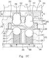
Fig. 2B-2C are schematic diagrams showing sectional views of the test strip reader module according toFig. 2A when the strip is inserted therein; -
Fig. 2D is a schematic diagram showing a sectional view of the test strip reader module according to another embodiment of the present invention; -
Figs. 3 is a schematic diagram showing a sectional view of the test strip reader module according to another embodiment of the present invention; -
Fig. 4 is a perspective view showing how the test strip reader module is assembled into an electronic device, according to the present invention. - Please refer to
Fig. 2A , which shows a perspective view showing a teststrip reader module 200 according to one embodiment of the present invention. The teststrip reader module 200 comprises acircuit board 280 and a modulemain body 240 disposed thereon. The modulemain body 240 includes anupper cover 245, and astrip insertion slot 210 is formed between the modulemain body 240 and theupper cover 245. The modulemain body 240 also includes twoelectrical contact portions 243 disposed at the location of thestrip insertion slot 210. The twoelectrical contact portions 243 can be electrically connected to corresponding electrodes (not shown) on atest strip 120 when inserted into thestrip insertion slot 210. Materials for theelectrical contact portions 243 and the corresponding electrodes are preferably of gold material such as the material used by Rightest® blood test strip accompanied with an embedded gold electrode technology (for example, the Validus® technology) to have better stability and conductivity. - Referring to
Figs. 2B and2C , which show sectional views of the teststrip reader module 200 illustrated inFig. 2A when thestrip 120 is inserted therein. The teststrip reader module 200 comprises the modulemain body 240 including theupper cover 245. As shown inFig. 2B , the modulemain body 240 and theupper cover 245 are formed integrally. An upperstrip contacting surface 212 and a lowerstrip contacting surface 214 can be defined in thestrip insertion slot 210. From a different point of view, a height H1 of thestrip insertion slot 210 for accommodating thetest strip 120 is defined by the upperstrip contacting surface 212 and the lowerstrip contacting surface 214 which makes the height ofstrip insertion slot 210 can be controlled by a single element since the height is defined when the modulemain body 240 was formed. In one embodiment of the present invention, the height H1 of thestrip insertion slot 210 can be defined as a standard thickness of thetest strip 120 plus a tolerance ranging between 0.05 and 0.5 millimeters. For example, the height H1 ranges between 1.05 and 1.5 millimeters when the standard thickness of thetest strip 120 is 1 millimeter. - The module
main body 240 also includes a firstoperation movement assembly 255 having anactuating element 250 for contacting acoding recess 122 on thetest strip 120 and ablocking element 260 disposed below the actuatingelement 250, and a secondoperation movement assembly 275 having aconductive element 270 disposed under theblocking element 260 and anelastic element 220 for pushing theconductive element 270 upward. It is appreciated that a set of the first and the second operation movement assemblies 255, 275 are contained in one ofoperation holes 242 of the modulemain body 240. Alternatively, in other embodiments, the firstoperation movement assembly 255 is disposed in oneoperation hole 242 while the secondoperation movement assembly 275 is accommodated in a supportingportion 295 of the modulemain body 240. - The
elastic element 220 can be, but not limited to, a spring, a metal elastic sheet or a metal dome. The shape of theconductive element 270 can be, but is not limited to, a column or ball-like element. The material of theconductive element 270 can be a metal material such as steel. The blockingelement 260 is made of an elastic material such as rubber or silicone. - According to
Figs 2B and2C , agrounding element 290 is disposed under theblocking element 260, and thecircuit board 280 has asignal source 282 providing an electronic signal Vs. It can be understood by the skilled person in the art that, under one condition that thetest strip 120 is not inserted into thestrip insertion slot 210, theconductive element 270 contacts thegrounding element 290 due to a push from theelastic element 220, and a conducting condition is formed when theconductive element 270 is in contact with thegrounding element 290 so the electronic signal Vs from thesignal source 282 can come all the way through a circuit via theconductive element 270 to thegrounding element 290. A current may exist in the circuit if the electronic signal is a voltage. When thetest strip 120 is inserted in thestrip insertion slot 210, as shown inFigs 2B and2C , theactuating element 250 is not pushed down if theactuating element 250 is located under thecorresponding coding recess 122 without aprotrusion portion 124. Consequently, the conducting condition occurs, which can be determined as a first encoding signal or a first read signal. - On the other hand, the
actuating element 250 in theoperation hole 242 is pushed down and theconductive element 270 is separated from thegrounding element 290 if theactuating element 250 is located under thecorresponding coding recess 122 having aprotrusion portion 124. According to one embodiment, a height H2 of theprotrusion portion 124 for pressing theactuation element 250 ranges between 0.4 and 0.8 millimeters. Consequently, a non-conducting condition is formed when theconductive element 270 is separated from thegrounding element 290 and the electronic signal Vs from thesignal source 282 cannot be transmitted to thegrounding element 290, which can be determined as a second encoding signal or a second read signal. Therefore, the read signal for acoding recess 122 at the corresponding position of theoperation hole 242 can be determined based on one of the conducting and the non-conducting conditions. One may decode or identify the coding of asingle recess 122 on thetest strip 120 based on whether the current is formed due to the electronic signal Vs from thesignal source 282 in thecircuit board 280. For instance in a binary coding system, one of the coding conditions can be zero while the other can be one, and vice versa. - Please refer to
Fig. 2D , which shows a sectional view of the test strip reader module according to another embodiment of the present invention. The operating concept for decoding the coding recesses 122 on thetest strips 120 inFig. 2D is similar to that of the embodiments illustrated inFigs. 2B and2C , and the difference is that each of the blockingelements 260 disposed in the operation holes 242 is operated independently. Deformation of asingle blocking element 260 due to the vertical movement of the correspondingactuating element 250 in response to the coding in the coding recesses 122 will not cause any influence on the movement of the blockingelements 260 in different operation holes 242, so the issue of misreading due to the influence of the movement ofadjacent actuating elements 250 may never exist. Aprotrusion 268 is formed in the blockingelement 260 at a location corresponding to theactuating element 250, and may have a shape to match that of theactuating element 250, so additional pressure from theactuating element 250 toward the blockingelement 260 is needed for allowing theactuating element 250 moving downward. In one embodiment, the portion of theconductive element 270 facing the blockingelement 260 is flat. Consequently, the movement ofconductive element 270 due to the compression of the blockingelement 260 becomes more precise, and thus the judgment for the reading signal will be more accurate. - In this embodiment, the blocking
element 260 includes afirst blocker 262 having a cantilever shape and asecond blocker 264 connected to thefirst blocker 262, and renders each of theactuating elements 250 disposed thereon can be moved independently without being effected by the movement in other operation holes 242 and causing a misread. In addition,first block 262 will deform when the blockingelement 260 is compressed by theactuating element 250, and thus additional pressure from theactuating element 250 will be needed for pushing theconductive element 270 downward to achieve more accurate code reading. Furthermore, contamination such as a particle (not shown) can be collected into an L-shapedcontamination collection portion 266 without effecting the electrical function down below when the contamination material accidently enters the teststrip reader module 200 via the operation holes 242. - Please refer to
Fig. 3 , which shows a sectional view of the teststrip reader module 300 when thetest strip 120 is inserted into thestrip insertion slot 210 according to another embodiment of the present invention, wherein the disposition of the elements such as thetest strip 120,circuit board 280, theupper cover 345 and themain module body 340 are similar to those in the descriptions set forth above, and the differences are in that the actuating element is replaced by an elongatedconductive element 350 having afirst end 352 for contacting the coding recesses 122, asecond end 354 for contacting theelastic element 220, aside groove 356 having afirst groove wall 357 near thefirst end 352 and asecond groove wall 358 disposed opposite to thefirst groove wall 357. Thesecond end 354 andelastic element 220 are contained in the supportingportion 395. According toFig. 3 , theconductive element 350 at the left side faces the correspondingcoding recess 122 without a protrusion, so theconductive element 350 at the left side is not compressed and thesecond groove wall 358 contacts thegrounding element 390 to form a conducting status which can be identified as a first encoding signal, while theconductive element 350 at the right side faces to thecorresponding coding recess 122 with aprotrusion 124, so theconductive element 350 at the right side is compressed and moves downward and forms a separation status with thegrounding element 390 which can be identified as a second encoding signal since the electronic signal Vs from thesignal source 282 in thecircuit board 280 cannot be transmitted to thegrounding element 390 to generate a current. The blockingelement 360 is preferably made of elastic material so it can be deformed along the vertical movement of theconductive element 350 while keeping a match condition with thefirst groove wall 357. Thesignal source 282 can include an ESD protection circuit for preventing the influence of electrostatic discharge caused by movement of theconductive element 350. - In addition to the dimensional variation due to element combination, the blocking elements may result in elastic fatigue and cause the test strip reader module operate abnormally. The present invention also provides solutions for avoiding the issue of contamination entering the inside of the reader module as described below.
- Referring again to
Fig. 3 , in which the actuating element inFigs. 2B-2D is replaced by theconductive element 350 having a cylinder-like shape while the operation holes 342 are sleeve-shaped, each of which contains oneconductive element 350. The blockingelement 360 includes afirst side wall 362 matching thefirst groove wall 357 of theconductive element 350 and deforming along with the vertical movement of theconductive element 350. Therefore, theconductive element 350 can operate independently without being affected by the otherconductive elements 350 in different operation holes 342. Acontamination collecting device 366 is formed between thefirst side wall 362 and a second side wall 364, as illustrated inFig. 3 . When a contamination P such as overflow sample, quality control fluid, ash or particles accidentally enters the teststrip reader module 300 from the operation holes 342, the contamination P will be contained in thecontamination collecting device 366 without falling into the lower portion of the modulemain body 340 and affecting the electrical function thereof. It can be appreciated by the skilled person in the art based onFig. 3 that thecontamination collecting device 366 has a shape of a groove surrounding theside groove 356 of theconductive element 350. - Please refer to
Fig. 4 , which shows how the teststrip reader module 200/300 according to the present invention is assembled into an electronic device. The teststrip reader module 200 itself has comprehensive functions for reading test strips, and can be connected to a communication module (not shown) disposed on a variety of mobile electronic devices such as cell phones, PDA or wearable electronic devices to allow the mobile electronic devices to analyze the analyte as well as transmitting the measurement data. The teststrip reader module 200 can be adapted to theassembly accessory 205 to be disposed between thetop cover 201 and the back over 202. Thetop cover 201 has an upper structure to accommodate the teststrip reader module 200 and optionally shelter theupper cover 245 partly or wholly for modifying the front appearance of the electronic device while allowing thestrip 120 to be easily inserted into the teststrip reader module 200. In one embodiment of the present invention, the teststrip reader module 200 has a thickness of about 12 millimeters which can be easily assembled. An electronic device furnished with the teststrip reader module 200 can readily have all the functions of the teststrip reader module 200.
Claims (9)
- A test strip reader (200, 300), comprising:a module main body (240, 340) including an upper cover (245), a grounding element (290, 390) and at least one operation hole (242, 342) containing a first operation movement assembly (255);a blocking element (260); anda circuit board (280),characterized in that:the first operation movement assembly (255) includes an actuating element (250),the module main body (240, 340) further includes a second operation movement assembly (275) having a conductive element (270) and an elastic element (220),the upper cover (245) and the module main body (240, 340) are formed integrally,whereby the test strip reader is configured such that a condition of one of a contact status and a separation status between the second operation movement assembly (275) and the grounding element (290, 390) determines a read signal,a conducting condition is formed when the conductive element (270) is in contact with the grounding element (290), a non-conducting condition is formed when the conductive element (270) is separated from the grounding element (290), andthe read signal for a coding recess (122) of a test trip (120) at the corresponding position of the operation hole (242, 342) is determined based on one of the conducting and the non-conducting conditions,whereby the conductive element (270) is disposed under the blocking element (260) and the elastic element (220) for pushing the conductive element (270) to contact with the grounding element (290, 390), and the actuating element (250) contacts the coding recess (122).
- The test strip reader (200, 300) as claimed in Claim 1, characterized in that the module main body (240, 340) further includes an upper strip contacting surface (212) and a lower strip contacting surface (214) to form a strip insertion slot (210) integrally with the module main body (240, 340) for accommodating a test strip (120).
- The test strip reader (200, 300) as claimed in Claim 2, characterized in that the strip insertion slot has a height (H1) being equal to a standard thickness of the test strip (120) plus a tolerance ranging between 0.05 and 0.5 millimeters.
- The test strip reader (200, 300) as claimed in Claim 2, characterized in that the test strip (120) includes at least one protrusion (124) having a protrusion height (H2) ranging between 0.4 and 0.8 millimeters.
- The test strip reader (200, 300) as claimed in Claim 1, characterized in that the circuit board (280) includes a signal source (282) providing an electronic signal Vs.
- The test strip reader (200, 300) as claimed in Claim 5, characterized in that the circuit board (280) is disposed below the elastic element (220).
- The test strip reader as claimed in Claim 6, characterized in that the first operation movement assembly (255) further includes a blocking element (260, 360) disposed below the actuating element (250).
- The test strip reader (200, 300) as claimed in Claim 7, characterized in that the blocking element (260, 360) includes a contamination-collecting portion (266, 366) formed of a first sidewall (262, 362) and a second sidewall (264, 364).
- The test strip reader (200, 300) as claimed in Claim 7, characterized in that the blocking element includes a protrusion (268) matching with the actuating element (250).
Applications Claiming Priority (1)
| Application Number | Priority Date | Filing Date | Title |
|---|---|---|---|
| TW105129875A TWI628438B (en) | 2016-09-13 | 2016-09-13 | Analyte measurement module |
Publications (2)
| Publication Number | Publication Date |
|---|---|
| EP3293519A1 EP3293519A1 (en) | 2018-03-14 |
| EP3293519B1 true EP3293519B1 (en) | 2021-05-19 |
Family
ID=59856410
Family Applications (1)
| Application Number | Title | Priority Date | Filing Date |
|---|---|---|---|
| EP17190413.9A Active EP3293519B1 (en) | 2016-09-13 | 2017-09-11 | A physiological parameter measurement module |
Country Status (3)
| Country | Link |
|---|---|
| US (1) | US10718752B2 (en) |
| EP (1) | EP3293519B1 (en) |
| TW (1) | TWI628438B (en) |
Families Citing this family (2)
| Publication number | Priority date | Publication date | Assignee | Title |
|---|---|---|---|---|
| US11852643B2 (en) * | 2020-10-13 | 2023-12-26 | Bionime Corporation | Physiological signal monitoring device |
| TWD223565S (en) * | 2022-03-04 | 2023-02-11 | 華廣生技股份有限公司 | Physiological signal monitoring device |
Family Cites Families (9)
| Publication number | Priority date | Publication date | Assignee | Title |
|---|---|---|---|---|
| TWI265677B (en) * | 2005-06-01 | 2006-11-01 | Bionime Corp | Coding module, bio measuring meter and system for operating bio measuring meter |
| DE102008029715B4 (en) * | 2008-06-23 | 2011-08-25 | Bionime Corporation, Taichung | Coding module, bio-meter and system for operating the bio-meter |
| KR101146900B1 (en) * | 2010-08-27 | 2012-05-23 | 주식회사 인포피아 | Apparatus for analyzing of biosensor |
| US8707392B2 (en) * | 2010-10-15 | 2014-04-22 | Roche Diagnostics Operations, Inc. | Systems and methods for disease management |
| US20120252133A1 (en) * | 2011-03-31 | 2012-10-04 | Cilag Gmbh International | Test meter with a strip port connector configured for fluid entrapment |
| KR101299795B1 (en) * | 2011-11-18 | 2013-08-23 | 주식회사 세라젬메디시스 | Biosensor having identification information and decipherment apparatus thereof |
| US9188561B2 (en) * | 2013-03-03 | 2015-11-17 | Yue Xu | Test strip |
| KR101425662B1 (en) * | 2013-03-05 | 2014-08-05 | 주식회사 세라젬메디시스 | Biosensor having identification information |
| US20150176053A1 (en) * | 2013-12-23 | 2015-06-25 | Cilag Gmbh International | Test strip insertion drive mechanism for analyte meter |
-
2016
- 2016-09-13 TW TW105129875A patent/TWI628438B/en not_active IP Right Cessation
-
2017
- 2017-09-11 EP EP17190413.9A patent/EP3293519B1/en active Active
- 2017-09-12 US US15/701,901 patent/US10718752B2/en active Active
Non-Patent Citations (1)
| Title |
|---|
| None * |
Also Published As
| Publication number | Publication date |
|---|---|
| US20180074041A1 (en) | 2018-03-15 |
| EP3293519A1 (en) | 2018-03-14 |
| TWI628438B (en) | 2018-07-01 |
| US10718752B2 (en) | 2020-07-21 |
| TW201812303A (en) | 2018-04-01 |
Similar Documents
| Publication | Publication Date | Title |
|---|---|---|
| EP2175531B1 (en) | Coaxial connector | |
| CN111952811B (en) | Connection method, connection structure, and connection terminal assembly | |
| CN108344771B (en) | Test piece reading device | |
| US20130012070A1 (en) | Card Connector | |
| CN101620944B (en) | Button switch | |
| KR101797654B1 (en) | Card socket for electronic device | |
| CN103367949B (en) | Card connector | |
| US9236695B2 (en) | Coaxial connector | |
| JP3148538U (en) | Card connector | |
| US10718752B2 (en) | Physiological parameter measurement module | |
| CN107817337B (en) | Analyte measuring module | |
| US8598481B2 (en) | Switch with sinuated air-passageway | |
| CN101345153A (en) | switch | |
| TWI607217B (en) | A physiological parameter measurement module | |
| CN107818275B (en) | Analyte measuring module | |
| US7372136B2 (en) | Chip card retaining mechanism | |
| JP5281538B2 (en) | Slide operation switch | |
| US20150269397A1 (en) | Card contact-making apparatus | |
| JP4595741B2 (en) | switch | |
| CN104701114A (en) | Switch | |
| KR101402999B1 (en) | Contact terminal for a sim card connector for wireless mobile terminal | |
| CN106104734B (en) | Button switch | |
| TWI803016B (en) | A test strip code reader and analyte detection device | |
| EP1667053A1 (en) | Memory pack | |
| JPH11251022A (en) | Contact pin of ic socket, contact pin unit and ic socket |
Legal Events
| Date | Code | Title | Description |
|---|---|---|---|
| PUAI | Public reference made under article 153(3) epc to a published international application that has entered the european phase |
Free format text: ORIGINAL CODE: 0009012 |
|
| STAA | Information on the status of an ep patent application or granted ep patent |
Free format text: STATUS: THE APPLICATION HAS BEEN PUBLISHED |
|
| AK | Designated contracting states |
Kind code of ref document: A1 Designated state(s): AL AT BE BG CH CY CZ DE DK EE ES FI FR GB GR HR HU IE IS IT LI LT LU LV MC MK MT NL NO PL PT RO RS SE SI SK SM TR |
|
| AX | Request for extension of the european patent |
Extension state: BA ME |
|
| STAA | Information on the status of an ep patent application or granted ep patent |
Free format text: STATUS: REQUEST FOR EXAMINATION WAS MADE |
|
| 17P | Request for examination filed |
Effective date: 20180913 |
|
| RBV | Designated contracting states (corrected) |
Designated state(s): AL AT BE BG CH CY CZ DE DK EE ES FI FR GB GR HR HU IE IS IT LI LT LU LV MC MK MT NL NO PL PT RO RS SE SI SK SM TR |
|
| STAA | Information on the status of an ep patent application or granted ep patent |
Free format text: STATUS: EXAMINATION IS IN PROGRESS |
|
| RIC1 | Information provided on ipc code assigned before grant |
Ipc: G01N 33/487 20060101AFI20200302BHEP |
|
| 17Q | First examination report despatched |
Effective date: 20200407 |
|
| GRAP | Despatch of communication of intention to grant a patent |
Free format text: ORIGINAL CODE: EPIDOSNIGR1 |
|
| STAA | Information on the status of an ep patent application or granted ep patent |
Free format text: STATUS: GRANT OF PATENT IS INTENDED |
|
| INTG | Intention to grant announced |
Effective date: 20210127 |
|
| RIN1 | Information on inventor provided before grant (corrected) |
Inventor name: LUI, TUNG-LIANG Inventor name: CHEN, MING-TA |
|
| GRAS | Grant fee paid |
Free format text: ORIGINAL CODE: EPIDOSNIGR3 |
|
| GRAA | (expected) grant |
Free format text: ORIGINAL CODE: 0009210 |
|
| STAA | Information on the status of an ep patent application or granted ep patent |
Free format text: STATUS: THE PATENT HAS BEEN GRANTED |
|
| AK | Designated contracting states |
Kind code of ref document: B1 Designated state(s): AL AT BE BG CH CY CZ DE DK EE ES FI FR GB GR HR HU IE IS IT LI LT LU LV MC MK MT NL NO PL PT RO RS SE SI SK SM TR |
|
| REG | Reference to a national code |
Ref country code: GB Ref legal event code: FG4D |
|
| REG | Reference to a national code |
Ref country code: CH Ref legal event code: EP |
|
| REG | Reference to a national code |
Ref country code: DE Ref legal event code: R096 Ref document number: 602017038739 Country of ref document: DE |
|
| REG | Reference to a national code |
Ref country code: AT Ref legal event code: REF Ref document number: 1394488 Country of ref document: AT Kind code of ref document: T Effective date: 20210615 |
|
| REG | Reference to a national code |
Ref country code: IE Ref legal event code: FG4D |
|
| REG | Reference to a national code |
Ref country code: LT Ref legal event code: MG9D |
|
| REG | Reference to a national code |
Ref country code: AT Ref legal event code: MK05 Ref document number: 1394488 Country of ref document: AT Kind code of ref document: T Effective date: 20210519 |
|
| REG | Reference to a national code |
Ref country code: NL Ref legal event code: MP Effective date: 20210519 |
|
| PG25 | Lapsed in a contracting state [announced via postgrant information from national office to epo] |
Ref country code: FI Free format text: LAPSE BECAUSE OF FAILURE TO SUBMIT A TRANSLATION OF THE DESCRIPTION OR TO PAY THE FEE WITHIN THE PRESCRIBED TIME-LIMIT Effective date: 20210519 Ref country code: LT Free format text: LAPSE BECAUSE OF FAILURE TO SUBMIT A TRANSLATION OF THE DESCRIPTION OR TO PAY THE FEE WITHIN THE PRESCRIBED TIME-LIMIT Effective date: 20210519 Ref country code: BG Free format text: LAPSE BECAUSE OF FAILURE TO SUBMIT A TRANSLATION OF THE DESCRIPTION OR TO PAY THE FEE WITHIN THE PRESCRIBED TIME-LIMIT Effective date: 20210819 Ref country code: AT Free format text: LAPSE BECAUSE OF FAILURE TO SUBMIT A TRANSLATION OF THE DESCRIPTION OR TO PAY THE FEE WITHIN THE PRESCRIBED TIME-LIMIT Effective date: 20210519 Ref country code: HR Free format text: LAPSE BECAUSE OF FAILURE TO SUBMIT A TRANSLATION OF THE DESCRIPTION OR TO PAY THE FEE WITHIN THE PRESCRIBED TIME-LIMIT Effective date: 20210519 |
|
| PG25 | Lapsed in a contracting state [announced via postgrant information from national office to epo] |
Ref country code: GR Free format text: LAPSE BECAUSE OF FAILURE TO SUBMIT A TRANSLATION OF THE DESCRIPTION OR TO PAY THE FEE WITHIN THE PRESCRIBED TIME-LIMIT Effective date: 20210820 Ref country code: IS Free format text: LAPSE BECAUSE OF FAILURE TO SUBMIT A TRANSLATION OF THE DESCRIPTION OR TO PAY THE FEE WITHIN THE PRESCRIBED TIME-LIMIT Effective date: 20210919 Ref country code: LV Free format text: LAPSE BECAUSE OF FAILURE TO SUBMIT A TRANSLATION OF THE DESCRIPTION OR TO PAY THE FEE WITHIN THE PRESCRIBED TIME-LIMIT Effective date: 20210519 Ref country code: PL Free format text: LAPSE BECAUSE OF FAILURE TO SUBMIT A TRANSLATION OF THE DESCRIPTION OR TO PAY THE FEE WITHIN THE PRESCRIBED TIME-LIMIT Effective date: 20210519 Ref country code: PT Free format text: LAPSE BECAUSE OF FAILURE TO SUBMIT A TRANSLATION OF THE DESCRIPTION OR TO PAY THE FEE WITHIN THE PRESCRIBED TIME-LIMIT Effective date: 20210920 Ref country code: NO Free format text: LAPSE BECAUSE OF FAILURE TO SUBMIT A TRANSLATION OF THE DESCRIPTION OR TO PAY THE FEE WITHIN THE PRESCRIBED TIME-LIMIT Effective date: 20210819 Ref country code: RS Free format text: LAPSE BECAUSE OF FAILURE TO SUBMIT A TRANSLATION OF THE DESCRIPTION OR TO PAY THE FEE WITHIN THE PRESCRIBED TIME-LIMIT Effective date: 20210519 Ref country code: SE Free format text: LAPSE BECAUSE OF FAILURE TO SUBMIT A TRANSLATION OF THE DESCRIPTION OR TO PAY THE FEE WITHIN THE PRESCRIBED TIME-LIMIT Effective date: 20210519 |
|
| PG25 | Lapsed in a contracting state [announced via postgrant information from national office to epo] |
Ref country code: NL Free format text: LAPSE BECAUSE OF FAILURE TO SUBMIT A TRANSLATION OF THE DESCRIPTION OR TO PAY THE FEE WITHIN THE PRESCRIBED TIME-LIMIT Effective date: 20210519 |
|
| PG25 | Lapsed in a contracting state [announced via postgrant information from national office to epo] |
Ref country code: ES Free format text: LAPSE BECAUSE OF FAILURE TO SUBMIT A TRANSLATION OF THE DESCRIPTION OR TO PAY THE FEE WITHIN THE PRESCRIBED TIME-LIMIT Effective date: 20210519 Ref country code: RO Free format text: LAPSE BECAUSE OF FAILURE TO SUBMIT A TRANSLATION OF THE DESCRIPTION OR TO PAY THE FEE WITHIN THE PRESCRIBED TIME-LIMIT Effective date: 20210519 Ref country code: EE Free format text: LAPSE BECAUSE OF FAILURE TO SUBMIT A TRANSLATION OF THE DESCRIPTION OR TO PAY THE FEE WITHIN THE PRESCRIBED TIME-LIMIT Effective date: 20210519 Ref country code: CZ Free format text: LAPSE BECAUSE OF FAILURE TO SUBMIT A TRANSLATION OF THE DESCRIPTION OR TO PAY THE FEE WITHIN THE PRESCRIBED TIME-LIMIT Effective date: 20210519 Ref country code: DK Free format text: LAPSE BECAUSE OF FAILURE TO SUBMIT A TRANSLATION OF THE DESCRIPTION OR TO PAY THE FEE WITHIN THE PRESCRIBED TIME-LIMIT Effective date: 20210519 Ref country code: SK Free format text: LAPSE BECAUSE OF FAILURE TO SUBMIT A TRANSLATION OF THE DESCRIPTION OR TO PAY THE FEE WITHIN THE PRESCRIBED TIME-LIMIT Effective date: 20210519 Ref country code: SM Free format text: LAPSE BECAUSE OF FAILURE TO SUBMIT A TRANSLATION OF THE DESCRIPTION OR TO PAY THE FEE WITHIN THE PRESCRIBED TIME-LIMIT Effective date: 20210519 |
|
| REG | Reference to a national code |
Ref country code: DE Ref legal event code: R097 Ref document number: 602017038739 Country of ref document: DE |
|
| PLBE | No opposition filed within time limit |
Free format text: ORIGINAL CODE: 0009261 |
|
| STAA | Information on the status of an ep patent application or granted ep patent |
Free format text: STATUS: NO OPPOSITION FILED WITHIN TIME LIMIT |
|
| 26N | No opposition filed |
Effective date: 20220222 |
|
| REG | Reference to a national code |
Ref country code: CH Ref legal event code: PL |
|
| REG | Reference to a national code |
Ref country code: BE Ref legal event code: MM Effective date: 20210930 |
|
| GBPC | Gb: european patent ceased through non-payment of renewal fee |
Effective date: 20210911 |
|
| PG25 | Lapsed in a contracting state [announced via postgrant information from national office to epo] |
Ref country code: IS Free format text: LAPSE BECAUSE OF FAILURE TO SUBMIT A TRANSLATION OF THE DESCRIPTION OR TO PAY THE FEE WITHIN THE PRESCRIBED TIME-LIMIT Effective date: 20210919 Ref country code: MC Free format text: LAPSE BECAUSE OF FAILURE TO SUBMIT A TRANSLATION OF THE DESCRIPTION OR TO PAY THE FEE WITHIN THE PRESCRIBED TIME-LIMIT Effective date: 20210519 Ref country code: AL Free format text: LAPSE BECAUSE OF FAILURE TO SUBMIT A TRANSLATION OF THE DESCRIPTION OR TO PAY THE FEE WITHIN THE PRESCRIBED TIME-LIMIT Effective date: 20210519 |
|
| PG25 | Lapsed in a contracting state [announced via postgrant information from national office to epo] |
Ref country code: LU Free format text: LAPSE BECAUSE OF NON-PAYMENT OF DUE FEES Effective date: 20210911 Ref country code: IT Free format text: LAPSE BECAUSE OF FAILURE TO SUBMIT A TRANSLATION OF THE DESCRIPTION OR TO PAY THE FEE WITHIN THE PRESCRIBED TIME-LIMIT Effective date: 20210519 Ref country code: IE Free format text: LAPSE BECAUSE OF NON-PAYMENT OF DUE FEES Effective date: 20210911 Ref country code: GB Free format text: LAPSE BECAUSE OF NON-PAYMENT OF DUE FEES Effective date: 20210911 Ref country code: FR Free format text: LAPSE BECAUSE OF NON-PAYMENT OF DUE FEES Effective date: 20210930 Ref country code: BE Free format text: LAPSE BECAUSE OF NON-PAYMENT OF DUE FEES Effective date: 20210930 |
|
| PG25 | Lapsed in a contracting state [announced via postgrant information from national office to epo] |
Ref country code: LI Free format text: LAPSE BECAUSE OF NON-PAYMENT OF DUE FEES Effective date: 20210930 Ref country code: CH Free format text: LAPSE BECAUSE OF NON-PAYMENT OF DUE FEES Effective date: 20210930 |
|
| PG25 | Lapsed in a contracting state [announced via postgrant information from national office to epo] |
Ref country code: HU Free format text: LAPSE BECAUSE OF FAILURE TO SUBMIT A TRANSLATION OF THE DESCRIPTION OR TO PAY THE FEE WITHIN THE PRESCRIBED TIME-LIMIT; INVALID AB INITIO Effective date: 20170911 |
|
| PG25 | Lapsed in a contracting state [announced via postgrant information from national office to epo] |
Ref country code: CY Free format text: LAPSE BECAUSE OF FAILURE TO SUBMIT A TRANSLATION OF THE DESCRIPTION OR TO PAY THE FEE WITHIN THE PRESCRIBED TIME-LIMIT Effective date: 20210519 |
|
| PG25 | Lapsed in a contracting state [announced via postgrant information from national office to epo] |
Ref country code: MK Free format text: LAPSE BECAUSE OF FAILURE TO SUBMIT A TRANSLATION OF THE DESCRIPTION OR TO PAY THE FEE WITHIN THE PRESCRIBED TIME-LIMIT Effective date: 20210519 |
|
| PG25 | Lapsed in a contracting state [announced via postgrant information from national office to epo] |
Ref country code: MT Free format text: LAPSE BECAUSE OF FAILURE TO SUBMIT A TRANSLATION OF THE DESCRIPTION OR TO PAY THE FEE WITHIN THE PRESCRIBED TIME-LIMIT Effective date: 20210519 |
|
| PGFP | Annual fee paid to national office [announced via postgrant information from national office to epo] |
Ref country code: DE Payment date: 20250912 Year of fee payment: 9 |
|
| PG25 | Lapsed in a contracting state [announced via postgrant information from national office to epo] |
Ref country code: TR Free format text: LAPSE BECAUSE OF FAILURE TO SUBMIT A TRANSLATION OF THE DESCRIPTION OR TO PAY THE FEE WITHIN THE PRESCRIBED TIME-LIMIT Effective date: 20210519 |