EP3292404B1 - Sensor chip with electrostatic discharge protection element - Google Patents
Sensor chip with electrostatic discharge protection element Download PDFInfo
- Publication number
- EP3292404B1 EP3292404B1 EP17702401.5A EP17702401A EP3292404B1 EP 3292404 B1 EP3292404 B1 EP 3292404B1 EP 17702401 A EP17702401 A EP 17702401A EP 3292404 B1 EP3292404 B1 EP 3292404B1
- Authority
- EP
- European Patent Office
- Prior art keywords
- protection element
- carrier
- sensor device
- encapsulation
- electronic component
- Prior art date
- Legal status (The legal status is an assumption and is not a legal conclusion. Google has not performed a legal analysis and makes no representation as to the accuracy of the status listed.)
- Active
Links
Images




Classifications
-
- G—PHYSICS
- G01—MEASURING; TESTING
- G01N—INVESTIGATING OR ANALYSING MATERIALS BY DETERMINING THEIR CHEMICAL OR PHYSICAL PROPERTIES
- G01N33/00—Investigating or analysing materials by specific methods not covered by groups G01N1/00 - G01N31/00
- G01N33/0004—Gaseous mixtures, e.g. polluted air
- G01N33/0009—General constructional details of gas analysers, e.g. portable test equipment
-
- G—PHYSICS
- G01—MEASURING; TESTING
- G01N—INVESTIGATING OR ANALYSING MATERIALS BY DETERMINING THEIR CHEMICAL OR PHYSICAL PROPERTIES
- G01N27/00—Investigating or analysing materials by the use of electric, electrochemical, or magnetic means
- G01N27/02—Investigating or analysing materials by the use of electric, electrochemical, or magnetic means by investigating impedance
- G01N27/04—Investigating or analysing materials by the use of electric, electrochemical, or magnetic means by investigating impedance by investigating resistance
- G01N27/12—Investigating or analysing materials by the use of electric, electrochemical, or magnetic means by investigating impedance by investigating resistance of a solid body in dependence upon absorption of a fluid; of a solid body in dependence upon reaction with a fluid, for detecting components in the fluid
- G01N27/121—Investigating or analysing materials by the use of electric, electrochemical, or magnetic means by investigating impedance by investigating resistance of a solid body in dependence upon absorption of a fluid; of a solid body in dependence upon reaction with a fluid, for detecting components in the fluid for determining moisture content, e.g. humidity, of the fluid
-
- H—ELECTRICITY
- H10—SEMICONDUCTOR DEVICES; ELECTRIC SOLID-STATE DEVICES NOT OTHERWISE PROVIDED FOR
- H10D—INORGANIC ELECTRIC SEMICONDUCTOR DEVICES
- H10D89/00—Aspects of integrated devices not covered by groups H10D84/00 - H10D88/00
- H10D89/60—Integrated devices comprising arrangements for electrical or thermal protection, e.g. protection circuits against electrostatic discharge [ESD]
Definitions
- the present idea refers to an electronic component and to a method for manufacturing an electronic component.
- sensors tend to be integrated into sensor chips in today's world of miniaturization.
- This kind of manufacturing is beneficial in that the size of a sensor device can significantly be reduced compared to a discrete type sensor and a sensing element of such a sensor can be arranged next to electronic circuitry integrated into the very same sensor chip which circuitry may include functions acting on a signal delivered by the sensing element such as amplification, evaluation, etc.
- DE 10 2007 029720 A1 relates to a simple, compact, and inexpensive design of a subassembly comprising at least one ASIC and a housing for the ASIC.
- the housing is fitted with terminals for externally connecting the ASIC by means of electric lines, while at least one electronic component is provided for protecting the ASIC against electrostatic discharges (ESD protection) and suppressing disturbance voltages (EMC) induced by means of the lines or terminals.
- ESD protection electrostatic discharges
- EMC disturbance voltages
- the at least one component is disposed inside the housing and is connected to at least one terminal.
- An electronic component according to the features of claim 1 comprises, and a method for manufacturing an electronic component according to claim 28 makes use of a sensor device which sensor device comprises a sensor chip.
- the sensor chip preferably is a semiconductor chip comprising a semiconductor substrate such as a silicon substrate, and preferably comprising a sensing element, for example sensitive to one or more of a chemical analyte, humidity, a flow of a fluid, a pressure, light or temperature.
- the sensor chip may, or may not comprise integrated circuitry connected to the sensing element.
- the sensor device may in one embodiment consist of the sensor chip, while in a different embodiment, the sensor device may in addition to the sensor chip comprise a package, such that the sensor device is represented by a packaged sensor chip. In a further embodiment the sensor device may comprise the sensor chip and additionally a cap substrate, for example. Preferably, and in particular in case the sensor chip is embodied for sensing an environmental measure such as humidity, a gas or pressure, the electronic component provides an access opening for allowing the medium to be measured to access the sensing element.
- an environmental measure such as humidity, a gas or pressure
- the sensor device is arranged on a carrier.
- the carrier supports the sensor device, and possibly one or more other elements, such as an IC, discrete electrical elements, a plug, etc.
- the carrier may be one of a printed circuit board, either in a non-flexible or in a flexible form, a ceramic circuit board, or a different kind of a circuit board allowing the elements carried to be electrically interconnected.
- the sensor device - and in particular its sensor chip - may be exposed to an electrostatic discharge from the environment which may damage the sensor chip.
- an electric discharge protection element - in short: protection element - is arranged on the carrier. This protection element provides for an effective protection of the sensor chip from such electric discharge.
- the protection element can be considered as a retrofit solution for protecting a sensor device originally lacking of an electric discharge protection.
- the protection element is an electrically conductive structure, and in particular is a metallic structure.
- the protection element may be punched from a sheet of metal, and be folded thereafter to the desired final shape.
- the material of the protection element may be tinned bronze.
- the protection element preferably is physically separated from the sensor chip, and preferably is also separated from the sensor device, such that there is no mechanical link there between other than via the carrier, of course, and, if applicable, by a common encapsulation.
- an efficient protection is realized by allowing an electric discharge being trapped by the protection element and being electrically isolated from the sensor chip.
- a minimum distance between the protection element and the sensor device is 0.1 mm. This is beneficial in preventing flash-arcs.
- the circuit board also comprises a contact, and preferably a contact pad for a ground connection, and preferably for ground connecting the electronic component.
- the protection element preferably is electrically connected to this contact for draining any electric discharge trapped to ground.
- the circuit board may include an electrically conducting path between the ground contact and the protection element.
- the protection element exceeds the sensor device in height. Hence, the protection element is more attractive to trap an electric discharge than the sensor chip and/or the sensor device, respectively.
- the protection element may comprises a rod including a single terminal mounted on the carrier.
- Such protection element includes a portion extending into a space above the sensor device.
- the protection element comprises a bridging structure including at least two, and preferably one of exactly two, three or four terminals resting on the carrier. Such protection element spans the sensor device at a distance. Such arrangement favors the trapping of electrical discharges. In addition, such protection element offers an enhanced mechanical stability given that the at least two of its terminals rest on the carrier.
- the bridging structure not only spans the sensor device but also one or more other chips in case such chips being present on the carrier.
- the sensor device is configured to sense a parameter of the environment, such as a flow of a fluid, light, temperature, gas, humidity, or pressure.
- a sensing element may be arranged on or integrated at a front side of the sensor chip which front side faces away from the carrier when the sensor chip is mounted onto the carrier.
- the sensing element requires an access to the environment for performing a sensing of the desired environmental variable.
- the sensor device comprises a package in addition to the sensor chip, the package preferably includes an access opening for allowing access to the sensing element.
- the package of the sensor device protects the sensor chip from mechanical impact and/or light, and may seal the chip against an undesired impact of liquids or gases.
- the package may cover at least parts of the sensor chip in form of an encapsulation, e.g. in form of a mold compound.
- the material used may preferably be a resist, in particular a dry resist, for example SU-8.
- the package may be an element formed separate from the chip and may be attached to the chip later on, for example, by gluing, bonding, etc.
- the package may be a silicon-on-insulator, or other semiconducting layer arrangement.
- the package may be made from one of a semiconductor, silicon, silicon and a silicon-oxide coating, silicon and a solderable coating, ceramic, ceramic and a silicon-oxide coating, ceramic and a solderable coating, glass, glass and a silicon-oxide coating, glass and a solderable coating, metal, metal and a solderable coating, dielectric material and a polymer.
- the sensor chip typically is arranged on a support such as a leadframe, which leadframe includes a die pad for arranging the sensor chip on, and contact pads electrically connected to the sensor chip, e.g. by means of bond wires.
- the encapsulation partly encapsulates the chip except for the access opening, and partly encapsulates the leadframe, e.g. except for the contact pads and/or the die pads.
- the access opening may take the form of a recess in the package thereby exposing the sensitive element to the outside world.
- the protection element has the shape of a bridging structure and at least partly bridges the sensor device
- the bridging structure is designed in geometry and arranged relative to the sensor device such that on the one hand an effective electric discharge protection is realized, and that on the other hand a sensing function of the sensor chip is not impaired by the protection element.
- the bridging structure spans an area of a top surface of the sensor device that is between a third and half of the entire top surface of the sensor device.
- the sensor device has a rectangular footprint owed to a typical rectangular footprint of the sensor chip diced out of a wafer.
- the sensor device preferably has contact pads exposed at least at a bottom surface of the sensor device, and preferably at edges of the sensor device.
- the sensor device only provides contact pads along two opposing edges of its footprint - also referred to as first pair of edges - such sensor device may also be referred to as DFN (Dual-Flat No-Leads).
- DFN Dual-Flat No-Leads
- QFN Quad-Flat No-Leads
- such sensor device is SMD-mounted (Surface Mounted Device) to the carrier.
- the carrier shows contact pads being prepared with a contact material such as a solder paste prior to the sensor device being placed onto the carrier.
- solder joints remain optically inspectable, and preferably automatically optically inspectable, for verifying the electrical connection between the sensor device and the carrier.
- the bridging structure is arranged on the carrier such that it does not affect the automated optical inspection of the electrical connections.
- the terminals of the bridging structure are arranged facing the sensor device at a second pair of opposed edges of its rectangular footprint.
- the sensor device may be represented by a QFN package even if optical inspection accessibility to two edges of the sensor device is limited owed to the arrangement of the bridging structure protection element.
- the bridging structure is arranged to bridge the sensor device in parallel to one of a longitudinal or lateral extension of the sensor chip, in a different embodiment, the bridging structure is arranged to bridge the sensor device diagonally.
- the protection element is a multi-use element.
- the protection element not only serves as an electric discharge protection element, but can also be used for mounting a housing to the carrier.
- the protection element in combination with a mounting element of the housing provides for a fixture for the housing.
- the mounting element on the housing side may include one or more clamps which are clamped to the protection element thereby securing the housing to the carrier.
- the housing may protect the sensor device and/or any further electronics from mechanical and/or fluid impact.
- the housing preferably is made from plastics and in a mounted state is clamped to the bridging structure.
- the sensor device and the protection element each are partly encapsulated by the same encapsulation.
- the sensor device includes a packaged sensor chip including the package and an access opening in the package.
- the sensor device does not consist of a bare semiconductor chip. However, it could apply to a capped semiconductor chip, e.g. capped by a silicon or other type cap.
- the encapsulation is applied after the sensor device and the protection element are arranged on the carrier such that the encapsulation at least partly encapsulates the sensor device and the protection element each, in view of the sensor device comprising the access opening in its package which preferably is not encapsulated by the encapsulation.
- the protection element remains uncovered from the encapsulation, and hence exposed in order to trap electrical charges.
- the encapsulation hence may encapsulate the package, however, e.g. leaving the access opening in the package uncovered.
- the encapsulation preferably also comprises an ingress via which ingress access to the sensor chip is granted. Accordingly, a medium to be measured may reach a sensing element of the sensor chip through the ingress of the encapsulation and through the access opening of the package. Accordingly, it is preferred that the access opening in the package and the ingress in the encapsulation are aligned, or at least are connected in order to allow the supply of the medium towards the sensing element. Given that the encapsulation is applied to the arrangement containing the sensor device and the protection element both attached to the carrier, it is preferred that the encapsulation also partly encapsulates the carrier.
- the encapsulation may protect the sensor device, and also the protection element.
- the encapsulation is created by a molding process, and specifically by one of
- the encapsulation is created by a hotmelt molding or potting process representing a low pressure injection molding process.
- the hotmelt which preferably is a thermoplastic adhesive, preferably is injected into the mold in a molten state and solidifies thereafter.
- the hotmelt may be one of Polyurethane, Polyamide, Polyolefine, Ethylen-Copolymere, Blockcopolymere or Polyester. This processing is preferred in that the sensor device is exposed to less heat and to less pressure than in injection molding.
- the mold remains at room temperature while the molten hotmelt preferably is injected into the mold at a temperature in a temperature range between 130° C and 180° C for a Polyurethane based hotmelt, and at a temperature in a temperature range between 180° C and 240° C for a Polyamide based hotmelt.
- a temperature at the devices to be molded remain significantly below these temperatures in view of the hotmelt cooling down immediately when meeting the device and acting as a thermal insulator while at the same time the mold acts as a heat sink.
- this molding process still offers a desired low viscosity of the hotmelt at reasonable temperatures.
- the hotmelt preferably partly encapsulates the cable and / or preferably the electrical connection between the cable and the carrier, too.
- the hotmelt can act as a protection element for the cable as well as any electrical or mechanical connection between the cable and the carrier. Since the solidified hotmelt still is a rather soft, it can react flexible on movement of the cable. In case the hotmelt adheres to the cable, it can absorb any tension or torsion stress acting on the cable.
- encapsulating the arrangement by a hotmelt is considered as a variant of molding given that for the subject purpose a mold is provided into which the material to be molded is injected / filled into.
- the package of the sensor device is manufactured by injection or transfer molding. Accordingly, it is preferred that different molding processes are applied sequentially for building the package first and the encapsulation thereafter.
- Transfer molding preferably makes use of a duroplast (Epoxide) as mold compound, which may be injected into the mold by a pressure up to a maximum of 100 bar. Injection molding is widely known and makes use of pressures up to 400 bar.
- the protection element shows a bridge structure and rests on the carrier with at least two terminals while a horizontal portion of the protection element bridges the access opening of the sensor device, it is preferred that such protection element also bridges the ingress.
- the horizontal portion of the bridges structure preferably extends above the access opening of the sensor device while it spans the ingress thereby, e.g. emerging from side walls of the encapsulation defining the ingress.
- the protection element may protrude from a top surface of the encapsulation and extends above the ingress.
- protection element is represented by single terminal element such as a rod.
- Such protection element may either emerge from a side wall of the encapsulation defining the ingress and reach into the ingress, or may emerge from a top surface of the encapsulation and be formed so as to reach into the space above the ingress. This may be achieved either by a pre-bent protection element, or by bending the protection element after having applied the encapsulation.
- the protection element may be bent by the mold used for encapsulating the sensor device, e.g. in response to closing the mold.
- a horizontal portion of the bridge spanning the ingress and the access opening may also be attributed a function during manufacturing the encapsulation:
- a part of the mold, and specifically a plunger used for forming the ingress preferably needs to cover the access opening of the sensor device to prevent molding compound or other contamination to access the sensor chip.
- the horizontal portion of the bridge structure may be arranged distant from the top surface of the sensor device and hence, distant from the access opening. Accordingly, it is preferred that the plunger not only rests on the horizontal portion of the protection element during molding but pushes the horizontal portion towards the top surface of the sensor device, and specifically towards the package including its access opening, in response to closing the mold.
- the horizontal portion of the protection element may at least partially rest or be in contact with the package of the sensor device such that it seals the access opening, or, in case the horizontal portion comprises an opening, that the plunger covers the opening while the horizontal portion seals the access opening.
- mold compound preferably is filled into the mold.
- the protection element is designed such its deformation evoked by the mold is not reversible and the protection element remains deformed after molding. In such state, the protection element preferably does not exert mechanical stress on the encapsulation.
- the protection element may be designed as elastic element such that its deformation evoked by the mold as such would be reversible. However, after the mold compound is solidified, the encapsulation urges the protection element to remain in its deformed state. In such state, the protection element may exert mechanical stress on the encapsulation.
- the elastic modulus of the protection element in combination with the dimensioning of the mold is selected such, that the mold is prevented from exerting exceeding pressure onto the sensor device when being closed.
- the protection element not only serves as an element for protecting the sensor chip from electric discharge, but at the same time protects the sensor chip and the entire sensor device during encapsulating the sensor device, and hence acts as a spacer during the encapsulation process.
- the horizontal portion of the protection element When the horizontal portion of the protection element is meant to rest on the sensor device after encapsulation, it is preferred that it has an opening that preferably is aligned with the access opening of the sensor device after encapsulating. This allows the medium to be measured to reach the access opening in the package and finally the sensing element.
- the plunger of the mold may - in the process of being moved towards the sensor device when closing the mold - capture a free end of the protection element on purpose, and thereby deform the protection element.
- the free end may be bent by the mold from its previous vertical position orthogonal to the plane of the carrier into a horizontal position in parallel to the plane of the carrier.
- a predetermined bending point in the protection element and / or a guide in the mold may support the desired deformation.
- the rod shaped protection element is not deformed on purpose during closing the mold but remains un-deformed.
- the plunger of the mold directly sits on the sensor device when the mold is closed, in order to cover the access opening.
- a mechanical impact of the mold may be alleviated by applying an elastic film either to the plunger, or to the sensor device, in any case spanning the access opening. Additionally, surface irregularities are balanced.
- Such elastic film may also be applied during molding in connection with the bridge structured protection element.
- the first variant where the film is attached to the mold is also known as film assisted molding. In the latter variant, the film may be permanently attached to the sensor device and not be removed after molding. Accordingly, such elastic film later on acts as a membrane for further protecting the sensor chip and shielding the access opening from contamination etc.
- Such material may be a perforated PTFE, for example.
- the protection element having a single terminal and a free end which is not deformed on purpose when applying the mold, it is preferred that after molding the encapsulation the free end emerging from the encapsulation is bent in order to bring it closer to the sensor chip. Preferably, the free end reaches into the ingress after bending. A middle portion of the protection element between the terminal and the free end remains encapsulated.
- a component is prefabricated which component contains a partly encapsulated protection element, the encapsulation of which is referred to as encapsulation member.
- encapsulation member a partly encapsulated protection element, the encapsulation of which is referred to as encapsulation member.
- the one or more terminals of the protection element is exposed.
- This component may then be mounted onto the carrier with its bottom surface facing a top surface of the carrier.
- the sensor device remains uncovered by the encapsulation member.
- the encapsulation member encircles the sensor device.
- a housing is provided for at least a part of the carrier.
- the sensor device preferably is premounted to the carrier.
- the housing e.g. in form of a plastic housing may have an opening in order to grant access to the sensor device.
- the protection element again is preferred to have a bridge structure, and to actually bridge the sensor device after being mounted to the carrier.
- at least two terminals of the protection element rest on the carrier and preferably are electrically connected thereto.
- each terminal may comprise an extension that preferably is arranged on a common level together with a horizontal portion of the protection element bridging the sensor.
- the protection element is attached to the carrier prior to the housing being attached to the carrier.
- the housing may finally be attached to the carrier by e.g. elements of the housing being clamped between the carrier and the extensions of the protection element.
- the housing may be brought into its desired position with respect to the carrier, and the extensions of the protection element may be bent into a form fit with the elements of the housing in order to fix the housing in this position.
- the electronic component is used in an automotive application.
- a method for manufacturing an electronic component.
- a sensor device is provided including contact pads as well as an electrostatic discharge protection element including at least one terminal. This order in providing the sensor device and the protection element is arbitrary and may be reversed.
- the sensor device is arranged on a carrier with the contact pads facing the carrier, and the protection element is arranged on the carrier with its one or more terminals facing the carrier. Again, this order is arbitrary and may be reversed.
- a common reflow soldering step is applied to both the sensor device and the protection element.
- the common reflow soldering step in particular may comprise a heating of a solder paste arranged between the contact pads / terminals of the sensor device and the protection element on the one hand and contact pads of the carrier on the other hand, thereby electrically and/or mechanically connecting the sensor device and the protection element to the carrier.
- an electronic component including a protection element for protecting from electrical discharge which protection element comprises at least one terminal mounted on and / or resting on the carrier.
- the protection element can be reflow soldered on the carrier together with the sensor device to protect from electrical discharge, or it can be pressed or snapped or clipped in or to the carrier by way of its one or more terminals.
- the protection element is shaped not to encase the sensor device.
- the protection element is not a closed structure in form of a cap capping the sensor device.
- the protection element preferably is shaped according to one or more of: not to fully encircle the sensor device; not comprising a wall in complete form fully encircling the sensor device; not of rectangular footprint.
- Embodiments disclosed in connection with the component shall also be considered disclosed in connection with the method and vice versa.
- FIG. 1 illustrates an electronic component according to an embodiment of the present invention.
- the electronic component includes at least an electric discharge protection element 1, a sensor device 2, and a carrier 3, but may contain additional elements not shown.
- the electronic component is shown in a perspective view in diagram a), in a side cut along line B - B' in diagram b), in a top view in diagram c), and in a side view in diagram d).
- the protection element 1 and the sensor device 2 are arranged on a front side of the carrier 3.
- the protection element 1 has the shape of a bridging structure that is arranged to bridge the sensor device 2.
- the protection element 1 contains two terminals 11 and 12 resting on the carrier 3.
- the bridging structure further includes two vertical portions 14 and 15, and a horizontal portion 13.
- the protection element 1 is a single piece made from a metal or any other electrically conducting material, and preferably is punched and bent into its present shape.
- the sensor device 2 is a packaged sensor chip 21 containing the sensor chip 21 and a package 22 in form of an encapsulation.
- the sensor chip 2 is arranged on a leadframe. Portions of the leadframe build contact pads 231 that are exposed at a bottom face of the sensor device 2 and as such face the carrier 3. In addition, portions of these contact pads 231 are exposed from side walls of the package 22 as can be seen in diagrams 1a) and 1b).
- the package 22 comprises an access opening 221 in form of a recess in a top surface of the package 22 for granting access to the sensor chip 2, and in particular for granting access to a sensitive element that is exposed from the package 22 by means of the access opening 221.
- the protection element 1 is electrically connected to a ground contact 31 of the carrier 3, via a conductor 32. Hence, any electrical discharge trapped by the protection element 1 is drained to the ground contact 31.
- a horizontal portion 13 of the protection element 1 spans the sensor device 2, and in particular spans a part of the access opening 221, since the exposed sensor chip 21 including the sensing element is most endangered by an electrical discharge. As can be seen from diagram 1c) it is not the entire surface of the sensor device 2 that is covered by the horizontal portion 13 of the protection element 1. Instead, a width w1 of the horizontal portion 13 is less than a width w2 of the sensor device 2 which ensures that the exposed portion of the sensor chip 2 receives a sufficient amount of the medium to be measured. Preferably, between a third and half of the top surface/footprint of the sensor device 2 is spanned by the protection element 1.
- the protection element 1 is arranged distant from the sensor device 2.
- a distance md which reflects a distance between a side wall of the sensor device 2 and the portion of the protection element 1 facing this side wall is equal to or less than 10 mm to prevent a direct discharge into the sensor device 2 on the one hand, and preferably is equal to or more than 0,05 mm, in order to prevent an arc-over on the one hand.
- the protection element 1 exceeds the sensor device 2 in height as can be derived from diagrams 1a) and 1b).
- a minimum height distance mh between the protection element 1 and the sensor device 2 is 1 mm.
- the contact pads 231 are arranged at an edge E1 of the sensor device 2 that does not face a terminal 11, 12 of the protection element 1.
- electrical connections - also referred to as solder joints in this context - between the carrier 3 and the contact pads 231 remain inspectable, and in particular optically inspectable.
- the sensor device 2 may comprise further contact pads 231 and solder joints at the opposed edge E2 which are optically inspectable in the same manner.
- FIG. 2 illustrates an electrical component according to an embodiment of the present invention.
- Diagram 2a) illustrates its perspective view
- diagram 2b) shows the electronic component in a lateral cut.
- the basic elements such as the protection element 1, the sensor device 2 and the carrier 3 may be identical to the ones shown in FIG. 1 , or may be of different shape and/or arrangement.
- the present electronic component includes a housing 4, e.g. made from plastics, only a portion of which housing 4 is shown, and which housing 4 shall protect the sensor device 2 and possibly any other elements arranged on the carrier 3.
- the housing 4 has two bars 41 and 42 forming an opening 43 there between.
- the bridge structured protection element 1 reaches into the opening 43, in particular with its horizontal portion 13, a top surface of which remains exposed to the outside world for trapping electrical discharges. Remainders of the opening not filled of the protection element 1 are dimensioned such that a sufficient amount of the medium reaches the sensor chip underneath.
- the two bars 41 and 42 each comprise an integrated clamp 411, 421, which clamp into the horizontal portion 13 of the protection element 1.
- the housing 4 and the carrier 3 are attached, such that the protection element 1 not only serves for draining an electric discharge but also serves for mounting the housing 4 to the carrier 3.
- the sensor device 2 comprises the sensor chip 21 arranged on a die pad 232 of a leadframe 32.
- contact portions 231 are made from the leadframe 23 and are connected to the sensor chip 2, e.g. by bond wires not shown.
- An encapsulation in form of a package 22 encloses portions of the sensor chip 21 and the leadframe 23.
- An access opening 221 in the package 22 provides access to a top surface of the sensor chip 21 including a sensitive element 211 being exposed through the access opening 221.
- the sensor chip 21 preferably is a semiconductor chip with a substrate, such as a silicon substrate, and a stack of material layers such as a CMOS layer stack on top of the substrate.
- the sensing element 211 is integrated into the sensor chip 21, e.g. is arranged in the stack of material layers in the present example.
- the sensing element 211 may be connected by means of at least two electrodes, such as interdigitated electrodes.
- the sensing element 211 may cover the electrodes.
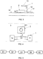
- FIG. 3 illustrates an electrical component in a side cut according to an embodiment of the present invention.
- the present protection element 1 is not of a bridge shape but rather of a rod shape including a single terminal 11 only.
- a vertical portion 12 holds a horizontal portion 13 reaching into a space above the sensor device 2 for providing an effective discharge protection.
- a height h1 of the protection element 1 exceeds a height h2 of the sensor device 2.
- the protection element 1 is arranged separate from the sensor device 2.
- the single terminal 11 in combination with the rest of the protection element 1 is configured in its dimension and / or weight such that a center of gravity of the protection element is configured to make the protection element 1 remain in an upright position after being placed on the carrier 3 for surface mounting.
- the overall shape of the protection element in this embodiment may be considered as a step.
- FIG. 4 illustrates an electrical component not in accordance with the present invention, in a top view.
- the protection element 1 again is bridge shaped such as in FIG. 1
- the protection element 1 now is arranged next to the sensor device 2, in particular at a distance d from the sensor device 2.
- This arrangement also provides an effective protection from an electric discharge.
- a housing (not shown) may be attached to the protection element 1 in the same manner as introduced with respect to FIG. 2 .
- FIG. 5 illustrates a method for manufacturing an electronic component according to an embodiment of the present invention.
- a sensor device is provided, the sensor device including contact pads.
- an electrostatic discharge protection element is provided, the protection element including at least one terminal.
- the sensor device is arranged on a carrier with the contact pads facing the carrier.
- the protection element is arranged on the carrier with the terminal facing the carrier.
- the contact pads and the at least one terminal are reflow soldered in a common reflow soldering step.
- Steps S1 and S2 can be interchanged in order.
- Steps S3 and S4 can be interchanged in order.
- Steps S1 and S3 can be performed in sequence, followed by steps S2 and S4.
- Steps S2 and S4 can be performed in sequence, followed by steps S1 and S3.
- the carrier is provided prepared, by having attached solder paste to the contact pads of the carrier the protection element and the sensor device are to be deposited on with their corresponding contact pads and terminals.
- a placement of the sensor device and the protection element onto the carrier includes a placement onto the solder paste.
- the common reflow soldering step may then include a heating of the solder paste for generating a sound electrical connection between the carrier and the sensor device and between the carrier and the protection element.
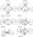
- FIGs. 6 to 10 each shows an electrical component in a top view, according to embodiments of the present invention.
- the protection element 1 is shaped as a bridging structure bridging a sensor device 2.
- the sensor device 2 preferably is a packaged sensor chip 21, but could take any other form of sensor device 2, too.
- the protection element 1 of FIG. 6 has four terminals 11, 12, 16 and 17 resting on the carrier. Accordingly, four vertical portions 14, 15, 18 and 19 are provided in the bridging structure, as well as a cross-shaped horizontal portion 13. This embodiment provides for an excellent mechanical stability.
- the protection element 1 of FIG. 7 has three terminals 11, 12 and 16 resting on the carrier. Accordingly, three vertical portions 14, 15, and 18 are provided in the bridging structure, as well as a T-shaped horizontal portion 13. This embodiment also provides for an excellent mechanical stability.
- the protection element 1 of FIG. 8 has two terminals 11, 12.
- the present horizontal portion 13 has cross-like extensions as such providing a bigger coverage of the sensor device 2 and as such providing an even better electric discharge protection.
- the protection element 1 of FIG. 9 has two terminals 11, 12, and a ring-shaped horizontal portion 13. Through the ring-shaped horizontal portion 13 an excellent access is provided to the sensor chip 21 for the medium to be measured, while at the same time the increased area of the ring-shaped horizontal portion 13 provides an excellent coverage of the sensor device 2 and as such provides an excellent electric discharge protection.
- the protection element 1 is identical to the protection element 1 of FIG. 9 . However, its orientation is different with respect to the sensor device 2. While in the embodiment of FIG. 9 , the basic orientation of the protection element 1 is in parallel to the edges of the sensor device 2 with its rectangular footprint, the protection element 1 of FIG. 10 is aligned diagonally across the sensor device 1. This orientation may also be implemented for any other shape of protection element 1.
- the protection element 1 is a single piece made from a metal or any other electrically conducting material, and preferably is punched and bent into its present shape.
- FIG. 11 illustrates an electrical component in a side cut, according to an embodiment of the present invention.
- the sensor device is represented by a sensor chip 21 with a sensing element 211 of the sensor chip 21 facing the carrier 3.
- the sensor chip 21 is flip-chip mounted onto the carrier 3 by means of e.g. solder balls 31. Access is granted to the sensing element 211 from side-ways - as indicated by the arrow - through a gap between the sensor chip 21 and the carrier 3.
- the protection element 1 bridges the sensor chip 2.
- FIG. 12 illustrates an electronic component in a cut view according to an embodiment of the present invention.
- the sensor device 1 is a packaged sensor chip comprising a package 22, contact pads 231 exposed from the package 22 and a sensor chip inside the package 22 (not visible). It is assumed that an access opening (not visible) is comprised in the package 22 in its top surface for granting access to a sensing element of the sensor chip.
- the protection element 1 is a bridge structure including a horizontal portion 13 extending in parallel to the plane of the carrier 3, which horizontal portion 13 spans the sensor device 2, and in particular spans the access opening.
- the protection element 1 extends beyond the terminals 11 and 12 and wraps around the carrier 3, thus, giving the protection element 1 the shape and function of a bracket.
- the protection element 1 may simply be clipped to the carrier 3.
- the terminals 11 and 12 may still be soldered to the carrier 3, in a different embodiment no such soldering is applied, and a sufficient electrical connection and mechanical support may be achieved just by the bracket shaped protection element 1 sitting tight on the carrier 3.
- the protection element 1 may be electrically connected to metallizations arranged on a backside / bottom surface of the carrier 3, i.e. opposite its front side / top surface to which the sensor device 2 is attached.
- the extensions wrapping around the carrier 3 can rather be considered as terminals 11 and 12.
- FIG. 13 illustrates another embodiment of an electronic component according to an embodiment of the present invention.
- the sensor device 2 preferably is a packaged sensor chip including an access opening (not visible).
- a housing 6, e.g. premanufactured, shall be attached to the carrier 3 thereby preferably being in contact with the carrier 3.
- the housing 6 does not cover the sensor device 2. Instead a gap is provided between the housing 6 and the sensor device 2.
- the protection element 1 is mounted to the carrier 3 carrying the sensor device 2 first.
- the protection element 1 preferably is a bridge structure so as to bridge the sensor device 2.
- the protection element 1 preferably shows extensions 111 and 121 at each of its terminals 11 and 12.
- extensions 111 preferably extend to a level elevated with respect to the level of the terminals 11 and 12.
- the housing 6 may be clipped or snapped under or otherwise attached to the extensions 111, 121 of the protection element 1.
- the extensions 111, 121 may be deformed in order to provide for a long lasting form-fit with the housing 6 thereby attaching the housing 6 to the carrier 3.
- the protection element 1 has two-fold functionality, i.e. ESD protection, and mechanical fixation at the same time.
- these extensions 111, 121 contribute to a form fit with the housing 6.
- the present protection element 1 may be prefabricated, e.g. by bending into the shape as shown.
- the level the extensions 111, 121 reach to the same level of the horizontal portion 13.
- the protection element 1 may comprise more than two terminals 11,12 and preferably is soldered by its two or more terminals 11,12 to corresponding metallizations of the carrier 3.
- the protection element 1 may instead by otherwise attached and electrically connected to the carrier 3.
- the housing 6 may provide means such as guides, snap fits, etc., to facilitate the orientation of the protection element on the carrier 3, and / or to support the attachment between the housing 6 and the protection element 1.
- FIG. 14 illustrates another embodiment of an electronic component according to an embodiment of the present invention.
- the sensor device 1 preferably is a packaged sensor device 2 including contact pads 231 and a package 22 partly covering a sensor chip, and an access opening (not visible) in the package 22 to allow a medium to be sensed to reach the sensor chip.
- the sensor device 2 is mounted to a carrier 3.
- a component comprising an encapsulation member 5 and a protection element 1 is not finally mounted to the carrier 3 yet.
- the component preferably is prefabricated, by partly encapsulating the protection element 1, preferably in a molding process.
- the encapsulation member 5 comprises a bottom surface presently facing a top surface of the carrier 3 the sensor device 2 is arranged on.
- the at least one terminal 11 of a first protection element 1 is exposed from the bottom surface of the encapsulation member 5 and the at least one terminal 12 of another first protection element 1' is exposed from the bottom surface of the encapsulation member 5 to enable mounting of the component to the top surface of the carrier 3 as is indicated by the arrows.
- the component preferably is prefabricated and mounted to the carrier 3 as a whole. In one embodiment, the component may be mounted to the carrier 3 solely by means of the one or more terminals 11 of the protection element 1, e.g. by soldering or pressing into or snapping into the carrier 3.
- the protection element 1 may, as presently shown, include two individual elements in form of rods, or a single protection element 1 including two or more terminals.
- each protection element 1 may be bent after being encapsulated as is shown in FIG. 14 .
- the protection element 1 as shown in FIG. 14 may be a single protection element 1 including a single terminal 11 encircling the sensor device 2 but not bridging it.
- the sensor device 2 is not in contact with the encapsulation member 5.
- the encapsulation member 5 can be considered to comprise an ingress 51 in form of an opening that allows medium to pass to the sensor device 2.
- the encapsulation member 5 includes additional mounting means such as snap fits to mount the component to the carrier 3.
- FIG. 15 illustrates another embodiment of an electronic component according to an embodiment of the present invention.
- the cut view in diagram 15b) resembles the electrical component of FIG. 1b ).
- a bridge structured protection element 1 bridges a packaged sensor device 2, the package 22 and contact pads 231 of which are shown.
- the protection element 1 includes a horizontal portion 13 spanning the sensor device 2, while terminals 11 and 12 rest on the carrier 3 and are electrically connected thereto. From the perspective view of diagram 15b) it can be derived that the present protection element 1 has an opening 131 in its horizontal portion 13 that allows access to the underlying access opening 221 of the sensor device 2.
- the electronic component of FIG. 15 may represent a complete electrical component, or may represent an intermediary product.
- FIG. 16 illustrates a method for manufacturing an electrical component according to an embodiment of the present invention, starting from the intermediary product of FIG. 15 :
- an arrangement including the sensor device 2 and the protection element 1 both mounted onto the carrier 3 is inserted in an (open state) of a mold 71,72 presently represented by a plunger 71 acting from the top and a support 72 acting from the bottom.
- the support 28 evokes an access to the backside of the carrier 3 in the future encapsulation.
- the support 72 of the mold may take different shapes subject to the needs.
- the support 72 may be supporting the entire backside of the carrier 3, such that the backside of the carrier 3 remains totally exposed from the future encapsulation.
- the support 72 may e.g. only engage with the sides of the carrier 3 such the backside of the carrier 3 becomes completely encapsulated by the future encapsulation.
- a mold compound is applied into / to the mold 71,72, preferably in form of a hotmelt, thereby generating an encapsulation 6.
- the mold not only consists of plunger 71 and support 72 but contains more elements (not shown) responsible for forming the outer shape of the encapsulation 6.
- the final product is illustrated in diagram 16d):
- the plunger 71 has caused an ingress 61 in the encapsulation 6 for the medium to be sensed to reach the sensor device 2, and in particular the sensor chip embedded in the sensor device 2.
- the access opening in the package 22 of the sensor device 2 opens to the top and leads into the ingress 61.
- Another recess 62 is built in the encapsulation 6 resulting from the support 72 of the mold 71,72, which in different embodiments may not be needed.
- the protection element 1 preferably is permanently deformed, in order to reduce mechanical stress in the encapsulation 6.
- FIGs. 17 and 18 illustrate modifications in the method for manufacturing the electronic component according to FIG. 16 according to embodiments of the present invention.
- the plunger 71 may be covered by an elastic film 711 that reduces mechanical stress on the protection element 1 during molding, and hence, protects the protection element 1.
- the elastic film 711 preferably is attached to the plunger 71 or is applied between the protection element 1 and the plunger 71, and will be removed after molding.
- an elastic film 8 is preferably placed on a top surface of the sensor device 2, i.e. between the sensor device 2 and the protection element 1.
- the film 8 protects the sensor device 2, and in particular its package 22. Since the film 8 is assumed to span the access opening in the package 22, it is preferred that the film 8 not only is elastic but also is permeable to the medium to be sensed given that it is not envisaged to remove the film 8 after molding.
- the elastic film can enhance a sealing of the access opening in the sensor device (not visible) in order to prevent hotmelt residuals to enter the access opening from the side while the plunger 71 is applied.
- the film 8 is removed after molding.
- the elastic film 8 as well as the elastic film 711 of FIG. 17 support the generation of smooth surfaces of the encapsulation.
- FIG. 19 illustrates another method for manufacturing an electronic component according to an embodiment of the present invention. Again it is started from an electrical component that in one embodiment is a final product, but in another embodiment represents an intermediary product that is similar to the intermediary product shown in FIG. 15 .
- a single terminal 11 protection element 1 in form of a rod is used and presently extends in z-direction orthogonal to the plane x / y defined by the carrier 3, see diagram 19a).
- the protection element 1 has the single terminal 11 by which it is mounted to the carrier 3, a free end If, and a middle portion 1m between the terminal 11 and the free end If.
- the arrangement of diagram 19a) is inserted into a mold containing a plunger 71, see diagram 19b).
- the mold may additionally contain a receptacle 712 for the rod shaped protection element 1, in particular its free end If.
- the mold may include multiple more shapes / elements.
- the plunger 71 does not directly act on the protection element 1 but sits on the sensor device 2 when being closed, optionally protected by an elastic film such as shown in FIG. 17 or in FIG. 18 .
- an encapsulation 6 is formed, see diagram 19c).
- the encapsulation 6 encloses the carrier 3, portions of the sensor device 2, but leaves an ingress 61 towards the sensor device 2.
- the protection element 1 protrudes from the encapsulation 6 by its free end If while the middle portion 1m thereof is covered and enclosed by the encapsulation 6.
- the free end If of the protection element 1 is bent into a horizontal position extending into the ingress 61 and hence improving its function as electrical discharge protection. It can be derived from diagram 19c), that the free end If terminates at the same level as the encapsulation 6: Hence, the free end If may be bent while the mold compound of the encapsulation 6 still is in a deformable state so as to press the free end If of the protection element 1 into the encapsulation 6.
- the plunger 71 includes a lateral protrusion to build a channel in the upper surface of the encapsulation 6 extending from the rim of the ingress 61 into which channel the free end If of the protection element 1 is bent, preferably after the mold compound is hardened.
- FIGs. 20 and 21 show modifications in the method of FIG. 19 and in the resulting electronic component, according to embodiments of the present invention.
- the final bending step is concerned.
- the free end If of the protection element 1 protrudes from the encapsulation 6 even after bending. Accordingly, it is assumed that the free end If is bent after the mold compound forming the encapsulation 6 is hardened.
- the bending is performed in the same manner as in the example of diagram 19c). However, two rod shaped protection elements 1 are provided instead of a single one. The free end If of each protection element 1 is bent towards the ingress 61 and reaches into the ingress 61.
- FIG. 22 shows a variant of FIG. 19b ): While there, a receptacle is provided in the mold for the rod shaped protection element that remains in its vertical position after molding, the receptacle 712 of FIG. 19b ) is not provided in the example of FIG. 22 . Instead, the free end If of the protection element 1 is pre-bent such that its free end is inclined towards the carrier 3 and will be bent when closing the mold halves, and preferably is bent towards the ingress in the encapsulation that will be produced by the plunger 71. Accordingly, in this embodiment, closing the mold and bending the protection element 1 is achieved in a single step.
Landscapes
- Chemical & Material Sciences (AREA)
- Health & Medical Sciences (AREA)
- Life Sciences & Earth Sciences (AREA)
- General Health & Medical Sciences (AREA)
- Immunology (AREA)
- Engineering & Computer Science (AREA)
- Analytical Chemistry (AREA)
- Biochemistry (AREA)
- Pathology (AREA)
- General Physics & Mathematics (AREA)
- Physics & Mathematics (AREA)
- Chemical Kinetics & Catalysis (AREA)
- Electrochemistry (AREA)
- Combustion & Propulsion (AREA)
- Food Science & Technology (AREA)
- Medicinal Chemistry (AREA)
- Pressure Sensors (AREA)
Description
- The present idea refers to an electronic component and to a method for manufacturing an electronic component.
- Subject to the application, sensors tend to be integrated into sensor chips in today's world of miniaturization. This kind of manufacturing is beneficial in that the size of a sensor device can significantly be reduced compared to a discrete type sensor and a sensing element of such a sensor can be arranged next to electronic circuitry integrated into the very same sensor chip which circuitry may include functions acting on a signal delivered by the sensing element such as amplification, evaluation, etc.
-
DE 10 2007 029720 A1 relates to a simple, compact, and inexpensive design of a subassembly comprising at least one ASIC and a housing for the ASIC. The housing is fitted with terminals for externally connecting the ASIC by means of electric lines, while at least one electronic component is provided for protecting the ASIC against electrostatic discharges (ESD protection) and suppressing disturbance voltages (EMC) induced by means of the lines or terminals. The at least one component is disposed inside the housing and is connected to at least one terminal. - Further background art is shown in
US 2011/278703 A1 ,GB 2 484 339 AUS 6 714 392 B2 ,US 5 407 854 A ,FR 3 014 094 A1JP 2012 242253 A - It is a general object of the invention to provide an electronic component including a sensor device with an improved electrostatic discharge protection.
- An electronic component according to the features of
claim 1 comprises, and a method for manufacturing an electronic component according to claim 28 makes use of a sensor device which sensor device comprises a sensor chip. The sensor chip preferably is a semiconductor chip comprising a semiconductor substrate such as a silicon substrate, and preferably comprising a sensing element, for example sensitive to one or more of a chemical analyte, humidity, a flow of a fluid, a pressure, light or temperature. The sensor chip may, or may not comprise integrated circuitry connected to the sensing element. - The sensor device may in one embodiment consist of the sensor chip, while in a different embodiment, the sensor device may in addition to the sensor chip comprise a package, such that the sensor device is represented by a packaged sensor chip. In a further embodiment the sensor device may comprise the sensor chip and additionally a cap substrate, for example. Preferably, and in particular in case the sensor chip is embodied for sensing an environmental measure such as humidity, a gas or pressure, the electronic component provides an access opening for allowing the medium to be measured to access the sensing element.
- The sensor device is arranged on a carrier. The carrier supports the sensor device, and possibly one or more other elements, such as an IC, discrete electrical elements, a plug, etc. The carrier may be one of a printed circuit board, either in a non-flexible or in a flexible form, a ceramic circuit board, or a different kind of a circuit board allowing the elements carried to be electrically interconnected.
- The sensor device - and in particular its sensor chip - may be exposed to an electrostatic discharge from the environment which may damage the sensor chip. In order to prevent such damage, an electric discharge protection element - in short: protection element - is arranged on the carrier. This protection element provides for an effective protection of the sensor chip from such electric discharge.
- In particular, if the sensor device itself does not include any electric discharge protection, the present approach allows for a still effective protection without the necessity to amend the design of the sensor device, and in particular the sensor chip. Hence, the protection element can be considered as a retrofit solution for protecting a sensor device originally lacking of an electric discharge protection.
- In a very preferred embodiment, the protection element is an electrically conductive structure, and in particular is a metallic structure. The protection element may be punched from a sheet of metal, and be folded thereafter to the desired final shape. The material of the protection element may be tinned bronze.
- The protection element preferably is physically separated from the sensor chip, and preferably is also separated from the sensor device, such that there is no mechanical link there between other than via the carrier, of course, and, if applicable, by a common encapsulation. By this means, an efficient protection is realized by allowing an electric discharge being trapped by the protection element and being electrically isolated from the sensor chip. Preferably, a minimum distance between the protection element and the sensor device is 0.1 mm. This is beneficial in preventing flash-arcs.
- In case of the carrier being a circuit board comprising circuit paths, it is preferred that the circuit board also comprises a contact, and preferably a contact pad for a ground connection, and preferably for ground connecting the electronic component. The protection element preferably is electrically connected to this contact for draining any electric discharge trapped to ground. The circuit board may include an electrically conducting path between the ground contact and the protection element.
- In a preferred embodiment, the protection element exceeds the sensor device in height. Hence, the protection element is more attractive to trap an electric discharge than the sensor chip and/or the sensor device, respectively.
- In a first alternative in accordance with the invention, the protection element may comprises a rod including a single terminal mounted on the carrier. Such protection element includes a portion extending into a space above the sensor device.
- In a second alternative, the protection element comprises a bridging structure including at least two, and preferably one of exactly two, three or four terminals resting on the carrier. Such protection element spans the sensor device at a distance. Such arrangement favors the trapping of electrical discharges. In addition, such protection element offers an enhanced mechanical stability given that the at least two of its terminals rest on the carrier. In a different embodiment, the bridging structure not only spans the sensor device but also one or more other chips in case such chips being present on the carrier.
- In a preferred embodiment, the sensor device is configured to sense a parameter of the environment, such as a flow of a fluid, light, temperature, gas, humidity, or pressure. In such example, a sensing element may be arranged on or integrated at a front side of the sensor chip which front side faces away from the carrier when the sensor chip is mounted onto the carrier.
- In many of the above applications, the sensing element requires an access to the environment for performing a sensing of the desired environmental variable. If in such case the sensor device comprises a package in addition to the sensor chip, the package preferably includes an access opening for allowing access to the sensing element. Preferably, the package of the sensor device protects the sensor chip from mechanical impact and/or light, and may seal the chip against an undesired impact of liquids or gases. In a preferred embodiment, the package may cover at least parts of the sensor chip in form of an encapsulation, e.g. in form of a mold compound. The material used may preferably be a resist, in particular a dry resist, for example SU-8. Or, the package may be an element formed separate from the chip and may be attached to the chip later on, for example, by gluing, bonding, etc. Here, the package may be a silicon-on-insulator, or other semiconducting layer arrangement. The package may be made from one of a semiconductor, silicon, silicon and a silicon-oxide coating, silicon and a solderable coating, ceramic, ceramic and a silicon-oxide coating, ceramic and a solderable coating, glass, glass and a silicon-oxide coating, glass and a solderable coating, metal, metal and a solderable coating, dielectric material and a polymer.
- In such sensor device, the sensor chip typically is arranged on a support such as a leadframe, which leadframe includes a die pad for arranging the sensor chip on, and contact pads electrically connected to the sensor chip, e.g. by means of bond wires. The encapsulation partly encapsulates the chip except for the access opening, and partly encapsulates the leadframe, e.g. except for the contact pads and/or the die pads. The access opening may take the form of a recess in the package thereby exposing the sensitive element to the outside world. If in such case the protection element has the shape of a bridging structure and at least partly bridges the sensor device, it is desired that the bridging structure is designed in geometry and arranged relative to the sensor device such that on the one hand an effective electric discharge protection is realized, and that on the other hand a sensing function of the sensor chip is not impaired by the protection element. In a preferred embodiment, the bridging structure spans an area of a top surface of the sensor device that is between a third and half of the entire top surface of the sensor device.
- Preferably, the sensor device has a rectangular footprint owed to a typical rectangular footprint of the sensor chip diced out of a wafer. The sensor device preferably has contact pads exposed at least at a bottom surface of the sensor device, and preferably at edges of the sensor device. In case the sensor device only provides contact pads along two opposing edges of its footprint - also referred to as first pair of edges - such sensor device may also be referred to as DFN (Dual-Flat No-Leads). In case the sensor device provides contact pads along all edges of its footprint such sensor device may also be referred to as QFN (Quad-Flat No-Leads).
- It is preferred, that such sensor device is SMD-mounted (Surface Mounted Device) to the carrier. The carrier shows contact pads being prepared with a contact material such as a solder paste prior to the sensor device being placed onto the carrier. After having placed the sensor device onto the carrier with its contact pads being aligned with the contact pads of the carrier and hence being deposited onto the solder paste, the electrical connections are established by heating the solder paste. In such scenario, it is preferred that solder joints remain optically inspectable, and preferably automatically optically inspectable, for verifying the electrical connection between the sensor device and the carrier.
- Taking the desire for an automated optical inspection of the electrical connections into account, it is preferred that the bridging structure is arranged on the carrier such that it does not affect the automated optical inspection of the electrical connections. Hence, in case of a DFN package with contact pads arranged along the first pair of edges, it is preferred that the terminals of the bridging structure are arranged facing the sensor device at a second pair of opposed edges of its rectangular footprint. However, in a different embodiment, the sensor device may be represented by a QFN package even if optical inspection accessibility to two edges of the sensor device is limited owed to the arrangement of the bridging structure protection element.
- While in one embodiment of the present invention - and provided the sensor chip has a rectangular footprint - the bridging structure is arranged to bridge the sensor device in parallel to one of a longitudinal or lateral extension of the sensor chip, in a different embodiment, the bridging structure is arranged to bridge the sensor device diagonally.
- In a preferred embodiment, the protection element is a multi-use element. The protection element not only serves as an electric discharge protection element, but can also be used for mounting a housing to the carrier. In particular when the protection element is embodied as a bridging structure, the protection element in combination with a mounting element of the housing provides for a fixture for the housing. The mounting element on the housing side may include one or more clamps which are clamped to the protection element thereby securing the housing to the carrier. The housing may protect the sensor device and/or any further electronics from mechanical and/or fluid impact. The housing preferably is made from plastics and in a mounted state is clamped to the bridging structure.
- The sensor device and the protection element each are partly encapsulated by the same encapsulation. Preferably, the sensor device includes a packaged sensor chip including the package and an access opening in the package. Preferably, the sensor device does not consist of a bare semiconductor chip. However, it could apply to a
capped semiconductor chip, e.g. capped by a silicon or other type cap. - Accordingly, in case of a sensor device including a packaged sensor chip, it is preferred that the encapsulation is applied after the sensor device and the protection element are arranged on the carrier such that the encapsulation at least partly encapsulates the sensor device and the protection element each, in view of the sensor device comprising the access opening in its package which preferably is not encapsulated by the encapsulation. On the other hand, at least a portion of the protection element remains uncovered from the encapsulation, and hence exposed in order to trap electrical charges. With respect to the sensor device, the encapsulation hence may encapsulate the package, however, e.g. leaving the access opening in the package uncovered. Hence, the encapsulation preferably also comprises an ingress via which ingress access to the sensor chip is granted. Accordingly, a medium to be measured may reach a sensing element of the sensor chip through the ingress of the encapsulation and through the access opening of the package. Accordingly, it is preferred that the access opening in the package and the ingress in the encapsulation are aligned, or at least are connected in order to allow the supply of the medium towards the sensing element. Given that the encapsulation is applied to the arrangement containing the sensor device and the protection element both attached to the carrier, it is preferred that the encapsulation also partly encapsulates the carrier.
- The encapsulation may protect the sensor device, and also the protection element.
- Preferably, the encapsulation is created by a molding process, and specifically by one of
- injection molding;
- low pressure injection molding;
- transfer molding;
- Most preferably, the encapsulation is created by a hotmelt molding or potting process representing a low pressure injection molding process. The hotmelt, which preferably is a thermoplastic adhesive, preferably is injected into the mold in a molten state and solidifies thereafter. The hotmelt may be one of Polyurethane, Polyamide, Polyolefine, Ethylen-Copolymere, Blockcopolymere or Polyester. This processing is preferred in that the sensor device is exposed to less heat and to less pressure than in injection molding. Preferably, in hotmelt molding the mold remains at room temperature while the molten hotmelt preferably is injected into the mold at a temperature in a temperature range between 130° C and 180° C for a Polyurethane based hotmelt, and at a temperature in a temperature range between 180° C and 240° C for a Polyamide based hotmelt. A temperature at the devices to be molded remain significantly below these temperatures in view of the hotmelt cooling down immediately when meeting the device and acting as a thermal insulator while at the same time the mold acts as a heat sink. However, this molding process still offers a desired low viscosity of the hotmelt at reasonable temperatures. One of the advantages is that owed to the lower pressure the hotmelt is injected into the mold - i.e. at pressures between 5 bar and 40 bar, compared to pressures of 100 bar to 1000 bar in injection molding - usage of an elastic film protecting structures during molding can be avoided. In case a cable e.g. is mounted or connected to the carrier, the hotmelt preferably partly encapsulates the cable and / or preferably the electrical connection between the cable and the carrier, too. Hence, the hotmelt can act as a protection element for the cable as well as any electrical or mechanical connection between the cable and the carrier. Since the solidified hotmelt still is a rather soft, it can react flexible on movement of the cable. In case the hotmelt adheres to the cable, it can absorb any tension or torsion stress acting on the cable.
- It is explicitly noted in this context that encapsulating the arrangement by a hotmelt is considered as a variant of molding given that for the subject purpose a mold is provided into which the material to be molded is injected / filled into.
- In contrast, it is preferred that the package of the sensor device is manufactured by injection or transfer molding. Accordingly, it is preferred that different molding processes are applied sequentially for building the package first and the encapsulation thereafter. Transfer molding preferably makes use of a duroplast (Epoxide) as mold compound, which may be injected into the mold by a pressure up to a maximum of 100 bar. Injection molding is widely known and makes use of pressures up to 400 bar.
- In case the protection element shows a bridge structure and rests on the carrier with at least two terminals while a horizontal portion of the protection element bridges the access opening of the sensor device, it is preferred that such protection element also bridges the ingress. Accordingly, the horizontal portion of the bridges structure preferably extends above the access opening of the sensor device while it spans the ingress thereby, e.g. emerging from side walls of the encapsulation defining the ingress. In a different embodiment, the protection element may protrude from a top surface of the encapsulation and extends above the ingress.
- The same holds in case the protection element is represented by single terminal element such as a rod. Such protection element may either emerge from a side wall of the encapsulation defining the ingress and reach into the ingress, or may emerge from a top surface of the encapsulation and be formed so as to reach into the space above the ingress. This may be achieved either by a pre-bent protection element, or by bending the protection element after having applied the encapsulation. In a third alternative, the protection element may be bent by the mold used for encapsulating the sensor device, e.g. in response to closing the mold.
- In case the protection element is of a bridge structure, a horizontal portion of the bridge spanning the ingress and the access opening may also be attributed a function during manufacturing the encapsulation: A part of the mold, and specifically a plunger used for forming the ingress, preferably needs to cover the access opening of the sensor device to prevent molding compound or other contamination to access the sensor chip. However, the horizontal portion of the bridge structure may be arranged distant from the top surface of the sensor device and hence, distant from the access opening. Accordingly, it is preferred that the plunger not only rests on the horizontal portion of the protection element during molding but pushes the horizontal portion towards the top surface of the sensor device, and specifically towards the package including its access opening, in response to closing the mold. Accordingly, during molding, the horizontal portion of the protection element may at least partially rest or be in contact with the package of the sensor device such that it seals the access opening, or, in case the horizontal portion comprises an opening, that the plunger covers the opening while the horizontal portion seals the access opening. In this state mold compound preferably is filled into the mold.
- In one embodiment, the protection element is designed such its deformation evoked by the mold is not reversible and the protection element remains deformed after molding. In such state, the protection element preferably does not exert mechanical stress on the encapsulation. In a different embodiment, the protection element may be designed as elastic element such that its deformation evoked by the mold as such would be reversible. However, after the mold compound is solidified, the encapsulation urges the protection element to remain in its deformed state. In such state, the protection element may exert mechanical stress on the encapsulation. In both scenarios, however, it is preferred that the elastic modulus of the protection element in combination with the dimensioning of the mold is selected such, that the mold is prevented from exerting exceeding pressure onto the sensor device when being closed. In this regard, the protection element not only serves as an element for protecting the sensor chip from electric discharge, but at the same time protects the sensor chip and the entire sensor device during encapsulating the sensor device, and hence acts as a spacer during the encapsulation process.
- When the horizontal portion of the protection element is meant to rest on the sensor device after encapsulation, it is preferred that it has an opening that preferably is aligned with the access opening of the sensor device after encapsulating. This allows the medium to be measured to reach the access opening in the package and finally the sensing element.
- In case the protection element is not bridge structured but rather an element containing a single terminal, the same concept may apply as indicated above: The plunger of the mold may - in the process of being moved towards the sensor device when closing the mold - capture a free end of the protection element on purpose, and thereby deform the protection element. In particular, the free end may be bent by the mold from its previous vertical position orthogonal to the plane of the carrier into a horizontal position in parallel to the plane of the carrier. A predetermined bending point in the protection element and / or a guide in the mold may support the desired deformation.
- However, in a different approach, the rod shaped protection element is not deformed on purpose during closing the mold but remains un-deformed. In this example, the plunger of the mold directly sits on the sensor device when the mold is closed, in order to cover the access opening.
- A mechanical impact of the mold may be alleviated by applying an elastic film either to the plunger, or to the sensor device, in any case spanning the access opening. Additionally, surface irregularities are balanced. Such elastic film may also be applied during molding in connection with the bridge structured protection element. The first variant where the film is attached to the mold is also known as film assisted molding. In the latter variant, the film may be permanently attached to the sensor device and not be removed after molding. Accordingly, such elastic film later on acts as a membrane for further protecting the sensor chip and shielding the access opening from contamination etc. In such case, it is desired to select a material of the film that not only is elastic but also is permeable to the medium to be measured, such as a gas or a liquid. Such material may be a perforated PTFE, for example.
- In case of the protection element having a single terminal and a free end which is not deformed on purpose when applying the mold, it is preferred that after molding the encapsulation the free end emerging from the encapsulation is bent in order to bring it closer to the sensor chip. Preferably, the free end reaches into the ingress after bending. A middle portion of the protection element between the terminal and the free end remains encapsulated.
- In a different approach, a component is prefabricated which component contains a partly encapsulated protection element, the encapsulation of which is referred to as encapsulation member. At a bottom surface of this encapsulation member, the one or more terminals of the protection element is exposed. This component may then be mounted onto the carrier with its bottom surface facing a top surface of the carrier. In one embodiment, it is only the one or more terminals of the protection element that provides for the mechanical mounting of the component to the carrier, which at the same time serves for an electrical connection to the carrier. In this approach, it is preferred that the sensor device remains uncovered by the encapsulation member. Preferably, the encapsulation member encircles the sensor device.
- In a different embodiment, a housing is provided for at least a part of the carrier. In this embodiment, the sensor device preferably is premounted to the carrier. The housing, e.g. in form of a plastic housing may have an opening in order to grant access to the sensor device. In this embodiment, the protection element again is preferred to have a bridge structure, and to actually bridge the sensor device after being mounted to the carrier. Again, at least two terminals of the protection element rest on the carrier and preferably are electrically connected thereto. However, each terminal may comprise an extension that preferably is arranged on a common level together with a horizontal portion of the protection element bridging the sensor. In a first variant, the protection element is attached to the carrier prior to the housing being attached to the carrier. Accordingly, the housing may finally be attached to the carrier by e.g. elements of the housing being clamped between the carrier and the extensions of the protection element. Or, the housing may be brought into its desired position with respect to the carrier, and the extensions of the protection element may be bent into a form fit with the elements of the housing in order to fix the housing in this position.
- Preferably, the electronic component is used in an automotive application.
- According to another aspect of the present invention, a method is provided for manufacturing an electronic component. A sensor device is provided including contact pads as well as an electrostatic discharge protection element including at least one terminal. This order in providing the sensor device and the protection element is arbitrary and may be reversed.
- The sensor device is arranged on a carrier with the contact pads facing the carrier, and the protection element is arranged on the carrier with its one or more terminals facing the carrier. Again, this order is arbitrary and may be reversed.
- Preferably, once both the sensor device and the protection element are arranged on the carrier, a common reflow soldering step is applied to both the sensor device and the protection element. The common reflow soldering step in particular may comprise a heating of a solder paste arranged between the contact pads / terminals of the sensor device and the protection element on the one hand and contact pads of the carrier on the other hand, thereby electrically and/or mechanically connecting the sensor device and the protection element to the carrier.
- This present idea results in an effective protection of the sensor chip including any circuitry from an electric discharge. Accordingly, an electronic component is provided including a protection element for protecting from electrical discharge which protection element comprises at least one terminal mounted on and / or resting on the carrier. The protection element can be reflow soldered on the carrier together with the sensor device to protect from electrical discharge, or it can be pressed or snapped or clipped in or to the carrier by way of its one or more terminals.
- Preferably, the protection element is shaped not to encase the sensor device. Hence, it is preferred that the protection element is not a closed structure in form of a cap capping the sensor device. Instead, the protection element preferably is shaped according to one or more of: not to fully encircle the sensor device; not comprising a wall in complete form fully encircling the sensor device; not of rectangular footprint.
- Embodiments disclosed in connection with the component shall also be considered disclosed in connection with the method and vice versa.
- Other advantageous embodiments are listed in the dependent claims as well as in the description below.
- The embodiments defined above and further embodiments, features and advantages of the present invention can also be derived from the examples of embodiments to be described hereinafter in connection with the drawings in which the figures illustrate:
-
FIG. 1 an electrical component according to an embodiment of the present invention, in diagram a) in a perspective view, in diagram b) in a side cut, in diagram c) in a top view, and in diagram d) in a side view; -
FIG. 2 an electrical component according to an embodiment of the present invention, in diagram a) in a perspective view, and in diagram b) in a lateral cut; -
FIG. 3 an electrical component in a side cut, according to an embodiment of the present invention; -
FIG. 4 an electrical component not encompassed by the present invention, in a top view; and -
FIG. 5 a method for manufacturing an electronic component according to an embodiment of the present invention; -
FIGs. 6 to 10 each an electrical component in a top view, according to embodiments of the present invention; -
FIGs. 11 to 14 each an electrical component in a side cut, according to an embodiment of the present invention, -
FIG. 15 an electrical component, in a side cut in diagram a) and in a perspective view in diagram b), according to an embodiment of the present invention; -
FIG. 16 a method for manufacturing an electrical component, according to an embodiment of the present invention; -
FIGs. 17 and 18 modifications in the method according toFIG. 16 , according to embodiments of the present invention; -
FIG. 19 another method for manufacturing an electrical component, according to an embodiment of the present invention; -
FIGs. 20, 21 and 22 modifications in the method and the resulting electronic component ofFIG. 19 , according to embodiments of the present invention. -
FIG. 1 illustrates an electronic component according to an embodiment of the present invention. The electronic component includes at least an electricdischarge protection element 1, asensor device 2, and acarrier 3, but may contain additional elements not shown. The electronic component is shown in a perspective view in diagram a), in a side cut along line B - B' in diagram b), in a top view in diagram c), and in a side view in diagram d). - The
carrier 3, for example, is a printed circuit board. Theprotection element 1 and thesensor device 2 are arranged on a front side of thecarrier 3. In the present embodiment, theprotection element 1 has the shape of a bridging structure that is arranged to bridge thesensor device 2. Theprotection element 1 contains twoterminals carrier 3. The bridging structure further includes twovertical portions horizontal portion 13. Theprotection element 1 is a single piece made from a metal or any other electrically conducting material, and preferably is punched and bent into its present shape. - The
sensor device 2 is a packagedsensor chip 21 containing thesensor chip 21 and apackage 22 in form of an encapsulation. Thesensor chip 2 is arranged on a leadframe. Portions of the leadframebuild contact pads 231 that are exposed at a bottom face of thesensor device 2 and as such face thecarrier 3. In addition, portions of thesecontact pads 231 are exposed from side walls of thepackage 22 as can be seen in diagrams 1a) and 1b). Thepackage 22 comprises an access opening 221 in form of a recess in a top surface of thepackage 22 for granting access to thesensor chip 2, and in particular for granting access to a sensitive element that is exposed from thepackage 22 by means of theaccess opening 221. - As can be derived from diagram 1b), the
protection element 1 is electrically connected to aground contact 31 of thecarrier 3, via aconductor 32. Hence, any electrical discharge trapped by theprotection element 1 is drained to theground contact 31. - A
horizontal portion 13 of theprotection element 1 spans thesensor device 2, and in particular spans a part of the access opening 221, since the exposedsensor chip 21 including the sensing element is most endangered by an electrical discharge. As can be seen from diagram 1c) it is not the entire surface of thesensor device 2 that is covered by thehorizontal portion 13 of theprotection element 1. Instead, a width w1 of thehorizontal portion 13 is less than a width w2 of thesensor device 2 which ensures that the exposed portion of thesensor chip 2 receives a sufficient amount of the medium to be measured. Preferably, between a third and half of the top surface/footprint of thesensor device 2 is spanned by theprotection element 1. - As can be seen from diagrams 1a) and 1b), the
protection element 1 is arranged distant from thesensor device 2. Preferably, a distance md, which reflects a distance between a side wall of thesensor device 2 and the portion of theprotection element 1 facing this side wall is equal to or less than 10 mm to prevent a direct discharge into thesensor device 2 on the one hand, and preferably is equal to or more than 0,05 mm, in order to prevent an arc-over on the one hand. - When it comes to a height relation between the
sensor device 2 and theprotection element 1, it is preferred that theprotection element 1 exceeds thesensor device 2 in height as can be derived from diagrams 1a) and 1b). In particular, a minimum height distance mh between theprotection element 1 and thesensor device 2 is 1 mm. - As can be derived from diagram 1a), the
contact pads 231 are arranged at an edge E1 of thesensor device 2 that does not face a terminal 11, 12 of theprotection element 1. Hence, electrical connections - also referred to as solder joints in this context - between thecarrier 3 and thecontact pads 231 remain inspectable, and in particular optically inspectable. Thesensor device 2 may comprisefurther contact pads 231 and solder joints at the opposed edge E2 which are optically inspectable in the same manner. -
FIG. 2 illustrates an electrical component according to an embodiment of the present invention. Diagram 2a) illustrates its perspective view, while diagram 2b) shows the electronic component in a lateral cut. The basic elements such as theprotection element 1, thesensor device 2 and thecarrier 3 may be identical to the ones shown inFIG. 1 , or may be of different shape and/or arrangement. In addition, the present electronic component includes ahousing 4, e.g. made from plastics, only a portion of whichhousing 4 is shown, and whichhousing 4 shall protect thesensor device 2 and possibly any other elements arranged on thecarrier 3. - The
housing 4 has twobars opening 43 there between. The bridge structuredprotection element 1 reaches into theopening 43, in particular with itshorizontal portion 13, a top surface of which remains exposed to the outside world for trapping electrical discharges. Remainders of the opening not filled of theprotection element 1 are dimensioned such that a sufficient amount of the medium reaches the sensor chip underneath. - The two
bars integrated clamp horizontal portion 13 of theprotection element 1. Hence, thehousing 4 and thecarrier 3 are attached, such that theprotection element 1 not only serves for draining an electric discharge but also serves for mounting thehousing 4 to thecarrier 3. - According to the cut view shown in diagram 2b), the
sensor device 2 comprises thesensor chip 21 arranged on adie pad 232 of aleadframe 32. In addition,contact portions 231 are made from theleadframe 23 and are connected to thesensor chip 2, e.g. by bond wires not shown. An encapsulation in form of apackage 22 encloses portions of thesensor chip 21 and theleadframe 23. An access opening 221 in thepackage 22 provides access to a top surface of thesensor chip 21 including asensitive element 211 being exposed through theaccess opening 221. - The
sensor chip 21 preferably is a semiconductor chip with a substrate, such as a silicon substrate, and a stack of material layers such as a CMOS layer stack on top of the substrate. Thesensing element 211 is integrated into thesensor chip 21, e.g. is arranged in the stack of material layers in the present example. Thesensing element 211 may be connected by means of at least two electrodes, such as interdigitated electrodes. Thesensing element 211 may cover the electrodes. -
FIG. 3 illustrates an electrical component in a side cut according to an embodiment of the present invention. In contrast to theprotection element 1 introduced inFIG. 1 , thepresent protection element 1 is not of a bridge shape but rather of a rod shape including asingle terminal 11 only. In addition, avertical portion 12 holds ahorizontal portion 13 reaching into a space above thesensor device 2 for providing an effective discharge protection. Notably, a height h1 of theprotection element 1 exceeds a height h2 of thesensor device 2. Theprotection element 1 is arranged separate from thesensor device 2. It is preferred, that thesingle terminal 11 in combination with the rest of theprotection element 1 is configured in its dimension and / or weight such that a center of gravity of the protection element is configured to make theprotection element 1 remain in an upright position after being placed on thecarrier 3 for surface mounting. The overall shape of the protection element in this embodiment may be considered as a step. -
FIG. 4 illustrates an electrical component not in accordance with the present invention, in a top view. Although theprotection element 1 again is bridge shaped such as inFIG. 1 , theprotection element 1 now is arranged next to thesensor device 2, in particular at a distance d from thesensor device 2. This arrangement also provides an effective protection from an electric discharge. A housing (not shown) may be attached to theprotection element 1 in the same manner as introduced with respect toFIG. 2 . -
FIG. 5 illustrates a method for manufacturing an electronic component according to an embodiment of the present invention. In step S1, a sensor device is provided, the sensor device including contact pads. In step S2, an electrostatic discharge protection element is provided, the protection element including at least one terminal. In step S3, the sensor device is arranged on a carrier with the contact pads facing the carrier. In step S4, the protection element is arranged on the carrier with the terminal facing the carrier. In step S5, the contact pads and the at least one terminal are reflow soldered in a common reflow soldering step. - Steps S1 and S2 can be interchanged in order. Steps S3 and S4 can be interchanged in order. Steps S1 and S3 can be performed in sequence, followed by steps S2 and S4. Steps S2 and S4 can be performed in sequence, followed by steps S1 and S3.
- In a preferred embodiment, the carrier is provided prepared, by having attached solder paste to the contact pads of the carrier the protection element and the sensor device are to be deposited on with their corresponding contact pads and terminals. Hence, a placement of the sensor device and the protection element onto the carrier includes a placement onto the solder paste. The common reflow soldering step may then include a heating of the solder paste for generating a sound electrical connection between the carrier and the sensor device and between the carrier and the protection element.
-
FIGs. 6 to 10 each shows an electrical component in a top view, according to embodiments of the present invention. In each of these embodiments, theprotection element 1 is shaped as a bridging structure bridging asensor device 2. Thesensor device 2 preferably is a packagedsensor chip 21, but could take any other form ofsensor device 2, too. - Instead of two
terminals protection element 1 ofFIG. 6 has fourterminals vertical portions horizontal portion 13. This embodiment provides for an excellent mechanical stability. - The
protection element 1 ofFIG. 7 has threeterminals vertical portions horizontal portion 13. This embodiment also provides for an excellent mechanical stability. - The
protection element 1 ofFIG. 8 has twoterminals horizontal portion 13 has cross-like extensions as such providing a bigger coverage of thesensor device 2 and as such providing an even better electric discharge protection. - The
protection element 1 ofFIG. 9 has twoterminals horizontal portion 13. Through the ring-shapedhorizontal portion 13 an excellent access is provided to thesensor chip 21 for the medium to be measured, while at the same time the increased area of the ring-shapedhorizontal portion 13 provides an excellent coverage of thesensor device 2 and as such provides an excellent electric discharge protection. - In the embodiment of
FIG. 10 , theprotection element 1 is identical to theprotection element 1 ofFIG. 9 . However, its orientation is different with respect to thesensor device 2. While in the embodiment ofFIG. 9 , the basic orientation of theprotection element 1 is in parallel to the edges of thesensor device 2 with its rectangular footprint, theprotection element 1 ofFIG. 10 is aligned diagonally across thesensor device 1. This orientation may also be implemented for any other shape ofprotection element 1. - Again, it is preferred that for any of the previous embodiments the
protection element 1 is a single piece made from a metal or any other electrically conducting material, and preferably is punched and bent into its present shape. -
FIG. 11 illustrates an electrical component in a side cut, according to an embodiment of the present invention. In this embodiment, the sensor device is represented by asensor chip 21 with asensing element 211 of thesensor chip 21 facing thecarrier 3. Hence, thesensor chip 21 is flip-chip mounted onto thecarrier 3 by means ofe.g. solder balls 31. Access is granted to thesensing element 211 from side-ways - as indicated by the arrow - through a gap between thesensor chip 21 and thecarrier 3. Theprotection element 1 bridges thesensor chip 2. -
FIG. 12 illustrates an electronic component in a cut view according to an embodiment of the present invention. Thesensor device 1 is a packaged sensor chip comprising apackage 22,contact pads 231 exposed from thepackage 22 and a sensor chip inside the package 22 (not visible). It is assumed that an access opening (not visible) is comprised in thepackage 22 in its top surface for granting access to a sensing element of the sensor chip. Similar to the embodiment ofFIG. 1 , theprotection element 1 is a bridge structure including ahorizontal portion 13 extending in parallel to the plane of thecarrier 3, whichhorizontal portion 13 spans thesensor device 2, and in particular spans the access opening. However, in this embodiment theprotection element 1 extends beyond theterminals carrier 3, thus, giving theprotection element 1 the shape and function of a bracket. Hence, in such embodiment, theprotection element 1 may simply be clipped to thecarrier 3. While in one embodiment, theterminals carrier 3, in a different embodiment no such soldering is applied, and a sufficient electrical connection and mechanical support may be achieved just by the bracket shapedprotection element 1 sitting tight on thecarrier 3. In an embodiment, theprotection element 1 may be electrically connected to metallizations arranged on a backside / bottom surface of thecarrier 3, i.e. opposite its front side / top surface to which thesensor device 2 is attached. In this embodiment, the extensions wrapping around thecarrier 3 can rather be considered asterminals -
FIG. 13 illustrates another embodiment of an electronic component according to an embodiment of the present invention. Again, thesensor device 2 preferably is a packaged sensor chip including an access opening (not visible). In this embodiment, ahousing 6, e.g. premanufactured, shall be attached to thecarrier 3 thereby preferably being in contact with thecarrier 3. Preferably, thehousing 6 does not cover thesensor device 2. Instead a gap is provided between thehousing 6 and thesensor device 2. In one embodiment, theprotection element 1 is mounted to thecarrier 3 carrying thesensor device 2 first. Theprotection element 1 preferably is a bridge structure so as to bridge thesensor device 2. However, theprotection element 1 preferably showsextensions terminals extensions 111 preferably extend to a level elevated with respect to the level of theterminals housing 6 may be clipped or snapped under or otherwise attached to theextensions protection element 1. In a possible final step, theextensions housing 6 thereby attaching thehousing 6 to thecarrier 3. Hence, theprotection element 1 has two-fold functionality, i.e. ESD protection, and mechanical fixation at the same time. In an assembled state, theseextensions housing 6. Thepresent protection element 1 may be prefabricated, e.g. by bending into the shape as shown. Preferably, the level theextensions horizontal portion 13. Theprotection element 1 may comprise more than twoterminals more terminals carrier 3. However, theprotection element 1 may instead by otherwise attached and electrically connected to thecarrier 3. In one embodiment, thehousing 6 may provide means such as guides, snap fits, etc., to facilitate the orientation of the protection element on thecarrier 3, and / or to support the attachment between thehousing 6 and theprotection element 1. -
FIG. 14 illustrates another embodiment of an electronic component according to an embodiment of the present invention. Again, thesensor device 1 preferably is a packagedsensor device 2 includingcontact pads 231 and apackage 22 partly covering a sensor chip, and an access opening (not visible) in thepackage 22 to allow a medium to be sensed to reach the sensor chip. In the state shown inFIG. 14 , thesensor device 2 is mounted to acarrier 3. A component comprising anencapsulation member 5 and aprotection element 1 is not finally mounted to thecarrier 3 yet. The component preferably is prefabricated, by partly encapsulating theprotection element 1, preferably in a molding process. Theencapsulation member 5 comprises a bottom surface presently facing a top surface of thecarrier 3 thesensor device 2 is arranged on. The at least oneterminal 11 of afirst protection element 1 is exposed from the bottom surface of theencapsulation member 5 and the at least oneterminal 12 of another first protection element 1' is exposed from the bottom surface of theencapsulation member 5 to enable mounting of the component to the top surface of thecarrier 3 as is indicated by the arrows. The component preferably is prefabricated and mounted to thecarrier 3 as a whole. In one embodiment, the component may be mounted to thecarrier 3 solely by means of the one ormore terminals 11 of theprotection element 1, e.g. by soldering or pressing into or snapping into thecarrier 3. Theprotection element 1 may, as presently shown, include two individual elements in form of rods, or asingle protection element 1 including two or more terminals. In case of one or more singleterminal protection elements 1, a free end of eachprotection element 1 may be bent after being encapsulated as is shown inFIG. 14 . In a different embodiment, theprotection element 1 as shown inFIG. 14 may be asingle protection element 1 including asingle terminal 11 encircling thesensor device 2 but not bridging it. Preferably, after mounting the component to thecarrier 3, thesensor device 2 is not in contact with theencapsulation member 5. Theencapsulation member 5 can be considered to comprise aningress 51 in form of an opening that allows medium to pass to thesensor device 2. Preferably, theencapsulation member 5 includes additional mounting means such as snap fits to mount the component to thecarrier 3. -
FIG. 15 illustrates another embodiment of an electronic component according to an embodiment of the present invention. The cut view in diagram 15b) resembles the electrical component ofFIG. 1b ). A bridge structuredprotection element 1 bridges a packagedsensor device 2, thepackage 22 andcontact pads 231 of which are shown. Theprotection element 1 includes ahorizontal portion 13 spanning thesensor device 2, whileterminals carrier 3 and are electrically connected thereto. From the perspective view of diagram 15b) it can be derived that thepresent protection element 1 has anopening 131 in itshorizontal portion 13 that allows access to the underlying access opening 221 of thesensor device 2. The electronic component ofFIG. 15 may represent a complete electrical component, or may represent an intermediary product. - In the latter case,
FIG. 16 illustrates a method for manufacturing an electrical component according to an embodiment of the present invention, starting from the intermediary product ofFIG. 15 : According to the diagram 16a), an arrangement including thesensor device 2 and theprotection element 1 both mounted onto thecarrier 3 is inserted in an (open state) of amold plunger 71 acting from the top and asupport 72 acting from the bottom. Presently, the support 28 evokes an access to the backside of thecarrier 3 in the future encapsulation. Of course, thesupport 72 of the mold may take different shapes subject to the needs. For example, thesupport 72 may be supporting the entire backside of thecarrier 3, such that the backside of thecarrier 3 remains totally exposed from the future encapsulation. In a different embodiment, thesupport 72 may e.g. only engage with the sides of thecarrier 3 such the backside of thecarrier 3 becomes completely encapsulated by the future encapsulation. - When closing the
mold plunger 71 and thesupport 72 towards each other, e.g. by clamping, theplunger 71 sits on thehorizontal portion 13 of theprotection element 1, and in the following deforms theprotection element 1. This deformed state of theprotection element 1 is shown in diagram 16b). It is assumed that closing themold sensor device 2 resulting in a damage. However, as can be derived from diagram 16b), the closing of themold horizontal portion 13 of theprotection element 1 at least partly resting on thesensor device 2, in particular on itspackage 22. - In the step shown in diagram 16c), a mold compound is applied into / to the
mold encapsulation 6. Of course, in this case the mold not only consists ofplunger 71 andsupport 72 but contains more elements (not shown) responsible for forming the outer shape of theencapsulation 6. The final product is illustrated in diagram 16d): Theplunger 71 has caused aningress 61 in theencapsulation 6 for the medium to be sensed to reach thesensor device 2, and in particular the sensor chip embedded in thesensor device 2. The access opening in thepackage 22 of thesensor device 2 opens to the top and leads into theingress 61. Anotherrecess 62 is built in theencapsulation 6 resulting from thesupport 72 of themold - As can be derived from diagram 16d), the
protection element 1 preferably is permanently deformed, in order to reduce mechanical stress in theencapsulation 6. -
FIGs. 17 and 18 illustrate modifications in the method for manufacturing the electronic component according toFIG. 16 according to embodiments of the present invention. According toFIG. 17 , theplunger 71 may be covered by anelastic film 711 that reduces mechanical stress on theprotection element 1 during molding, and hence, protects theprotection element 1. Theelastic film 711 preferably is attached to theplunger 71 or is applied between theprotection element 1 and theplunger 71, and will be removed after molding. - According to
FIG. 18 , anelastic film 8 is preferably placed on a top surface of thesensor device 2, i.e. between thesensor device 2 and theprotection element 1. When theplunger 71 exerts pressure on thehorizontal portion 13 of theprotection element 1 and pushes it towards thesensor device 2, thefilm 8 protects thesensor device 2, and in particular itspackage 22. Since thefilm 8 is assumed to span the access opening in thepackage 22, it is preferred that thefilm 8 not only is elastic but also is permeable to the medium to be sensed given that it is not envisaged to remove thefilm 8 after molding. In addition, the elastic film can enhance a sealing of the access opening in the sensor device (not visible) in order to prevent hotmelt residuals to enter the access opening from the side while theplunger 71 is applied. In a different embodiment, thefilm 8 is removed after molding. In addition, theelastic film 8 as well as theelastic film 711 ofFIG. 17 support the generation of smooth surfaces of the encapsulation. -
FIG. 19 illustrates another method for manufacturing an electronic component according to an embodiment of the present invention. Again it is started from an electrical component that in one embodiment is a final product, but in another embodiment represents an intermediary product that is similar to the intermediary product shown inFIG. 15 . Instead of the bridge structuredprotection element 1 ofFIG. 15 , asingle terminal 11protection element 1 in form of a rod is used and presently extends in z-direction orthogonal to the plane x / y defined by thecarrier 3, see diagram 19a). Theprotection element 1 has thesingle terminal 11 by which it is mounted to thecarrier 3, a free end If, and amiddle portion 1m between the terminal 11 and the free end If. - In a next step the arrangement of diagram 19a) is inserted into a mold containing a
plunger 71, see diagram 19b). The mold may additionally contain areceptacle 712 for the rod shapedprotection element 1, in particular its free end If. However, the mold may include multiple more shapes / elements. Theplunger 71 does not directly act on theprotection element 1 but sits on thesensor device 2 when being closed, optionally protected by an elastic film such as shown inFIG. 17 or inFIG. 18 . After having applied a mold compound, anencapsulation 6 is formed, see diagram 19c). Theencapsulation 6 encloses thecarrier 3, portions of thesensor device 2, but leaves aningress 61 towards thesensor device 2. Theprotection element 1 protrudes from theencapsulation 6 by its free end If while themiddle portion 1m thereof is covered and enclosed by theencapsulation 6. - In a next step shown in diagram 19d), the free end If of the
protection element 1 is bent into a horizontal position extending into theingress 61 and hence improving its function as electrical discharge protection. It can be derived from diagram 19c), that the free end If terminates at the same level as the encapsulation 6: Hence, the free end If may be bent while the mold compound of theencapsulation 6 still is in a deformable state so as to press the free end If of theprotection element 1 into theencapsulation 6. In a different embodiment, theplunger 71 includes a lateral protrusion to build a channel in the upper surface of theencapsulation 6 extending from the rim of theingress 61 into which channel the free end If of theprotection element 1 is bent, preferably after the mold compound is hardened. -
FIGs. 20 and 21 show modifications in the method ofFIG. 19 and in the resulting electronic component, according to embodiments of the present invention. In each of the embodiments, the final bending step is concerned. In the embodiment ofFIG. 20 , the free end If of theprotection element 1 protrudes from theencapsulation 6 even after bending. Accordingly, it is assumed that the free end If is bent after the mold compound forming theencapsulation 6 is hardened. In the embodiment ofFIG. 21 , the bending is performed in the same manner as in the example of diagram 19c). However, two rod shapedprotection elements 1 are provided instead of a single one. The free end If of eachprotection element 1 is bent towards theingress 61 and reaches into theingress 61. -
FIG. 22 shows a variant ofFIG. 19b ): While there, a receptacle is provided in the mold for the rod shaped protection element that remains in its vertical position after molding, thereceptacle 712 ofFIG. 19b ) is not provided in the example ofFIG. 22 . Instead, the free end If of theprotection element 1 is pre-bent such that its free end is inclined towards thecarrier 3 and will be bent when closing the mold halves, and preferably is bent towards the ingress in the encapsulation that will be produced by theplunger 71. Accordingly, in this embodiment, closing the mold and bending theprotection element 1 is achieved in a single step. - While there are shown and described presently preferred embodiments of the invention, it is to be distinctly understood that the invention is not limited thereto but may be otherwise variously embodied and practiced within the scope of the following claims.
Claims (15)
- Electronic component, comprising
a carrier (3),
a sensor device (2) mounted on the carrier (3), which sensor device (2) comprises a sensor chip (21),
an electrostatic discharge protection element (1) for protecting the sensor chip (21) from an electrostatic discharge, which protection element (1) is mounted on the carrier (3),
an encapsulation (6) partly encapsulating the sensor device (2), and partly encapsulating the protection element (1),
wherein the protection element (1) comprises a bridging structure including at least two terminals (11,12) resting on the carrier (3) and wherein the protection element (1) is arranged to bridge the sensor device (2), or
wherein the protection element (1) comprises a rod including a single terminal (11) mounted on the carrier (3) and wherein the rod includes a portion (13) extending into a space above the sensor device (2). - Electronic component according to claim 1,
wherein the sensor device (2) comprises a package (22) in addition to the sensor chip (21),
preferably wherein the sensor chip (21) comprises a sensing element (211) arranged on or integrated at a front side of the sensor chip (21),
preferably wherein the package (22) comprises an access opening (221) for providing access to the sensing element (211) from the outside,
preferably wherein the protection element (1) is physically separated from the sensor device (2). - Electronic component according to claim 2,
wherein the protection element (1) is arranged to bridge at least a part of the access opening (221). - Electronic component according to claim 1,
wherein the single terminal (11) is configured in its dimension and / or weight that the protection element (1) remains in an upright position after being placed on the carrier (3) for surface mounting. - Electronic component according to any one of the preceding claims,
wherein the carrier (3) is a circuit board, and in particular a printed circuit board,
wherein the carrier (3) comprises a contact (31) for a ground connection, and
wherein the protection element (1) is electrically connected to the contact (31) for ground connection. - Electronic component according to any one of the preceding claims,
wherein the encapsulation (6) partly encapsulates the carrier (3). - Electronic component according to claim 3,
wherein the encapsulation (6) comprises an ingress (61) for providing access to the sensing element (211),
wherein the protection element (1) is arranged to emerge from the encapsulation (6) and to at least partly bridge the ingress (61). - Electronic component according to claim 7,
wherein a portion of the protection element (1) rests on the sensor device (2). - Electronic component according to any of the preceding claims,
wherein the protection element (1) exhibits a deformation resulting from manufacturing the encapsulation (6). - Electronic component according to claim 4,
wherein a free end (1f) of the protection element (1) protrudes from the encapsulation (6),
in particular wherein the free end (1f) extends in parallel to a plane extension of the carrier (3),
in particular wherein a portion (1m) of the protection element (1) between the free end (1f) and the terminal (11) extends orthogonal to the plane extension of the carrier (3) and represents the portion of the protection element (1) that is encapsulated by the encapsulation (6). - Method for manufacturing an electronic component, comprising
providing a sensor device (2) including contact pads (231),
providing an electrostatic discharge protection element (1) including at least one terminal (11),
arranging the sensor device (2) on a carrier (3) with the contact pads facing the carrier (3),
arranging the protection element (1) on the carrier (3) with the at least one terminal (11) facing the carrier (3) wherein the protection element (1) comprises a bridging structure including at least two terminals (11,12) the protection element (1) is arranged to bridge the sensor device (2) and the at least two terminals rest on the carrier, or wherein the protection element (1) comprises a rod including a single terminal (11) a portion (13) of the rod extends into a space above the sensor device (2) and the single terminal (11) is mounted on the carrier (3),
forming an encapsulation (6) partly encapsulating the sensor device (2) arranged on the carrier (3), and partly encapsulating the protection element (1) arranged on the carrier (3). - Method according to claim 11, comprising
forming the encapsulation (6) by one of:- injection molding;- low pressure injection molding, preferably hotmelt molding or potting;- transfer molding. - Method according to claim 11 or claim 12, comprising
forming the encapsulation (6) to comprise an ingress (61) for providing access to the sensing element (211),
wherein the encapsulation (6) is formed to make the protection element (1) emerge from the encapsulation (6). - Method according to claim 13, comprising
forming the encapsulation (6) by arranging the carrier (3) carrying the sensor device (2) and the protection element (1) into a mold (71,72) comprising a plunger (71) for pressing onto the protection element (1), and
filling the mold (71,72) by a mold compound resulting in the encapsulation (6) including the ingress (61) formed by means of the plunger (71),
in particular wherein the mold (71,72) is dimensioned with respect to the carrier (3) carrying the sensor device (2) and the protection element (1) to deform the protection element (1) by the plunger (71) in response to closing the mold (71,72),
preferably wherein the protection element (1) remains deformed after molding. - Method according to claim 14,
wherein the protection element (1) comprises the bridging structure including the at least two terminals (11,12) resting on the carrier (3),
wherein the encapsulation (6) is formed to make the protection element (1) at least partly bridge the ingress (61),
preferably wherein a horizontal portion (13) of the protection element (1) rests on the sensor device (2) after molding,
preferably wherein the horizontal portion (13) of the protection element (1) rests on the package (22) of the sensor device (2) after molding.
Applications Claiming Priority (3)
| Application Number | Priority Date | Filing Date | Title |
|---|---|---|---|
| EP2016155356 | 2016-02-11 | ||
| EP2016163475 | 2016-04-01 | ||
| PCT/EP2017/052404 WO2017137325A1 (en) | 2016-02-11 | 2017-02-03 | Sensor chip with electrostatic discharge protection element |
Publications (2)
| Publication Number | Publication Date |
|---|---|
| EP3292404A1 EP3292404A1 (en) | 2018-03-14 |
| EP3292404B1 true EP3292404B1 (en) | 2019-05-22 |
Family
ID=57944447
Family Applications (1)
| Application Number | Title | Priority Date | Filing Date |
|---|---|---|---|
| EP17702401.5A Active EP3292404B1 (en) | 2016-02-11 | 2017-02-03 | Sensor chip with electrostatic discharge protection element |
Country Status (1)
| Country | Link |
|---|---|
| EP (1) | EP3292404B1 (en) |
Families Citing this family (1)
| Publication number | Priority date | Publication date | Assignee | Title |
|---|---|---|---|---|
| CN113629089B (en) * | 2021-08-06 | 2023-12-01 | 武汉新芯集成电路制造有限公司 | Semiconductor device and manufacturing method thereof |
Citations (1)
| Publication number | Priority date | Publication date | Assignee | Title |
|---|---|---|---|---|
| US20080150050A1 (en) * | 2006-12-26 | 2008-06-26 | Lightuning Tech. Inc. | Information sensing device and method of manufacturing the same |
-
2017
- 2017-02-03 EP EP17702401.5A patent/EP3292404B1/en active Active
Patent Citations (1)
| Publication number | Priority date | Publication date | Assignee | Title |
|---|---|---|---|---|
| US20080150050A1 (en) * | 2006-12-26 | 2008-06-26 | Lightuning Tech. Inc. | Information sensing device and method of manufacturing the same |
Also Published As
| Publication number | Publication date |
|---|---|
| EP3292404A1 (en) | 2018-03-14 |
Similar Documents
| Publication | Publication Date | Title |
|---|---|---|
| US11022590B2 (en) | Electronic component including sensor device and method of manufacturing same | |
| AU2009307832B2 (en) | Integrated sensor including sensing and processing die mounted on opposite sides of package substrate | |
| KR100636580B1 (en) | Semiconductor acceleration sensor device and method for manufacturing the same | |
| EP0502710B1 (en) | Flexible film semiconductor package | |
| CA1040747A (en) | Integrated circuit package utilizing novel heat sink structure | |
| KR100559062B1 (en) | Semiconductor device and its manufacturing method | |
| US20140210062A1 (en) | Leadframe-Based Semiconductor Package Having Terminals on Top and Bottom Surfaces | |
| CN104422558B (en) | Die edge protection for pressure sensor packages | |
| US9475691B1 (en) | Molded package structure with glue bleed stopper for sealing a MEMs device method of packaging a MEMs device | |
| EP3396329A1 (en) | Sensor package | |
| US10118816B2 (en) | Method of forming a protective coating for a packaged semiconductor device | |
| US7056765B2 (en) | Semiconductor device package and method of manufacture | |
| US6147398A (en) | Semiconductor device package | |
| US5963782A (en) | Semiconductor component and method of manufacture | |
| EP3292404A1 (en) | Sensor chip with electrostatic discharge protection element | |
| US20030001250A1 (en) | TCP optical device | |
| GB2396963A (en) | Semiconductor packaging structure | |
| US20220085004A1 (en) | Electronic device | |
| KR101744351B1 (en) | Sensor module and sensor module arrangement | |
| JPH1038730A (en) | Pressure sensor and pressure detector using the same | |
| TWI712177B (en) | Micromechanical pressure sensor | |
| KR940008559B1 (en) | Manufacturing method and apparatus of sensor deivce | |
| JPH0491475A (en) | Semiconductor chip and semiconductor integrated circuit device using same | |
| KR19980058302A (en) | Multichip Package Method | |
| KR19980015937A (en) | Resin dam - Lead frame with bar formed |
Legal Events
| Date | Code | Title | Description |
|---|---|---|---|
| STAA | Information on the status of an ep patent application or granted ep patent |
Free format text: STATUS: UNKNOWN |
|
| STAA | Information on the status of an ep patent application or granted ep patent |
Free format text: STATUS: THE INTERNATIONAL PUBLICATION HAS BEEN MADE |
|
| PUAI | Public reference made under article 153(3) epc to a published international application that has entered the european phase |
Free format text: ORIGINAL CODE: 0009012 |
|
| STAA | Information on the status of an ep patent application or granted ep patent |
Free format text: STATUS: REQUEST FOR EXAMINATION WAS MADE |
|
| 17P | Request for examination filed |
Effective date: 20171205 |
|
| AK | Designated contracting states |
Kind code of ref document: A1 Designated state(s): AL AT BE BG CH CY CZ DE DK EE ES FI FR GB GR HR HU IE IS IT LI LT LU LV MC MK MT NL NO PL PT RO RS SE SI SK SM TR |
|
| AX | Request for extension of the european patent |
Extension state: BA ME |
|
| STAA | Information on the status of an ep patent application or granted ep patent |
Free format text: STATUS: EXAMINATION IS IN PROGRESS |
|
| 17Q | First examination report despatched |
Effective date: 20180329 |
|
| RAP1 | Party data changed (applicant data changed or rights of an application transferred) |
Owner name: SENSIRON AUTOMOTIVE SOLUTIONS AG |
|
| RAP1 | Party data changed (applicant data changed or rights of an application transferred) |
Owner name: SENSIRION AUTOMOTIVE SOLUTIONS AG |
|
| GRAP | Despatch of communication of intention to grant a patent |
Free format text: ORIGINAL CODE: EPIDOSNIGR1 |
|
| STAA | Information on the status of an ep patent application or granted ep patent |
Free format text: STATUS: GRANT OF PATENT IS INTENDED |
|
| INTG | Intention to grant announced |
Effective date: 20181219 |
|
| GRAS | Grant fee paid |
Free format text: ORIGINAL CODE: EPIDOSNIGR3 |
|
| GRAJ | Information related to disapproval of communication of intention to grant by the applicant or resumption of examination proceedings by the epo deleted |
Free format text: ORIGINAL CODE: EPIDOSDIGR1 |
|
| GRAL | Information related to payment of fee for publishing/printing deleted |
Free format text: ORIGINAL CODE: EPIDOSDIGR3 |
|
| STAA | Information on the status of an ep patent application or granted ep patent |
Free format text: STATUS: EXAMINATION IS IN PROGRESS |
|
| GRAP | Despatch of communication of intention to grant a patent |
Free format text: ORIGINAL CODE: EPIDOSNIGR1 |
|
| STAA | Information on the status of an ep patent application or granted ep patent |
Free format text: STATUS: GRANT OF PATENT IS INTENDED |
|
| INTC | Intention to grant announced (deleted) | ||
| INTG | Intention to grant announced |
Effective date: 20190304 |
|
| GRAA | (expected) grant |
Free format text: ORIGINAL CODE: 0009210 |
|
| STAA | Information on the status of an ep patent application or granted ep patent |
Free format text: STATUS: THE PATENT HAS BEEN GRANTED |
|
| DAV | Request for validation of the european patent (deleted) | ||
| DAX | Request for extension of the european patent (deleted) | ||
| AK | Designated contracting states |
Kind code of ref document: B1 Designated state(s): AL AT BE BG CH CY CZ DE DK EE ES FI FR GB GR HR HU IE IS IT LI LT LU LV MC MK MT NL NO PL PT RO RS SE SI SK SM TR |
|
| REG | Reference to a national code |
Ref country code: GB Ref legal event code: FG4D |
|
| REG | Reference to a national code |
Ref country code: CH Ref legal event code: EP |
|
| REG | Reference to a national code |
Ref country code: IE Ref legal event code: FG4D |
|
| REG | Reference to a national code |
Ref country code: DE Ref legal event code: R096 Ref document number: 602017004144 Country of ref document: DE |
|
| REG | Reference to a national code |
Ref country code: AT Ref legal event code: REF Ref document number: 1136725 Country of ref document: AT Kind code of ref document: T Effective date: 20190615 |
|
| REG | Reference to a national code |
Ref country code: NL Ref legal event code: MP Effective date: 20190522 |
|
| REG | Reference to a national code |
Ref country code: LT Ref legal event code: MG4D |
|
| PG25 | Lapsed in a contracting state [announced via postgrant information from national office to epo] |
Ref country code: PT Free format text: LAPSE BECAUSE OF FAILURE TO SUBMIT A TRANSLATION OF THE DESCRIPTION OR TO PAY THE FEE WITHIN THE PRESCRIBED TIME-LIMIT Effective date: 20190922 Ref country code: HR Free format text: LAPSE BECAUSE OF FAILURE TO SUBMIT A TRANSLATION OF THE DESCRIPTION OR TO PAY THE FEE WITHIN THE PRESCRIBED TIME-LIMIT Effective date: 20190522 Ref country code: NO Free format text: LAPSE BECAUSE OF FAILURE TO SUBMIT A TRANSLATION OF THE DESCRIPTION OR TO PAY THE FEE WITHIN THE PRESCRIBED TIME-LIMIT Effective date: 20190822 Ref country code: SE Free format text: LAPSE BECAUSE OF FAILURE TO SUBMIT A TRANSLATION OF THE DESCRIPTION OR TO PAY THE FEE WITHIN THE PRESCRIBED TIME-LIMIT Effective date: 20190522 Ref country code: ES Free format text: LAPSE BECAUSE OF FAILURE TO SUBMIT A TRANSLATION OF THE DESCRIPTION OR TO PAY THE FEE WITHIN THE PRESCRIBED TIME-LIMIT Effective date: 20190522 Ref country code: AL Free format text: LAPSE BECAUSE OF FAILURE TO SUBMIT A TRANSLATION OF THE DESCRIPTION OR TO PAY THE FEE WITHIN THE PRESCRIBED TIME-LIMIT Effective date: 20190522 Ref country code: NL Free format text: LAPSE BECAUSE OF FAILURE TO SUBMIT A TRANSLATION OF THE DESCRIPTION OR TO PAY THE FEE WITHIN THE PRESCRIBED TIME-LIMIT Effective date: 20190522 Ref country code: LT Free format text: LAPSE BECAUSE OF FAILURE TO SUBMIT A TRANSLATION OF THE DESCRIPTION OR TO PAY THE FEE WITHIN THE PRESCRIBED TIME-LIMIT Effective date: 20190522 Ref country code: FI Free format text: LAPSE BECAUSE OF FAILURE TO SUBMIT A TRANSLATION OF THE DESCRIPTION OR TO PAY THE FEE WITHIN THE PRESCRIBED TIME-LIMIT Effective date: 20190522 |
|
| PG25 | Lapsed in a contracting state [announced via postgrant information from national office to epo] |
Ref country code: BG Free format text: LAPSE BECAUSE OF FAILURE TO SUBMIT A TRANSLATION OF THE DESCRIPTION OR TO PAY THE FEE WITHIN THE PRESCRIBED TIME-LIMIT Effective date: 20190822 Ref country code: RS Free format text: LAPSE BECAUSE OF FAILURE TO SUBMIT A TRANSLATION OF THE DESCRIPTION OR TO PAY THE FEE WITHIN THE PRESCRIBED TIME-LIMIT Effective date: 20190522 Ref country code: LV Free format text: LAPSE BECAUSE OF FAILURE TO SUBMIT A TRANSLATION OF THE DESCRIPTION OR TO PAY THE FEE WITHIN THE PRESCRIBED TIME-LIMIT Effective date: 20190522 Ref country code: GR Free format text: LAPSE BECAUSE OF FAILURE TO SUBMIT A TRANSLATION OF THE DESCRIPTION OR TO PAY THE FEE WITHIN THE PRESCRIBED TIME-LIMIT Effective date: 20190823 |
|
| REG | Reference to a national code |
Ref country code: AT Ref legal event code: MK05 Ref document number: 1136725 Country of ref document: AT Kind code of ref document: T Effective date: 20190522 |
|
| PG25 | Lapsed in a contracting state [announced via postgrant information from national office to epo] |
Ref country code: DK Free format text: LAPSE BECAUSE OF FAILURE TO SUBMIT A TRANSLATION OF THE DESCRIPTION OR TO PAY THE FEE WITHIN THE PRESCRIBED TIME-LIMIT Effective date: 20190522 Ref country code: AT Free format text: LAPSE BECAUSE OF FAILURE TO SUBMIT A TRANSLATION OF THE DESCRIPTION OR TO PAY THE FEE WITHIN THE PRESCRIBED TIME-LIMIT Effective date: 20190522 Ref country code: RO Free format text: LAPSE BECAUSE OF FAILURE TO SUBMIT A TRANSLATION OF THE DESCRIPTION OR TO PAY THE FEE WITHIN THE PRESCRIBED TIME-LIMIT Effective date: 20190522 Ref country code: CZ Free format text: LAPSE BECAUSE OF FAILURE TO SUBMIT A TRANSLATION OF THE DESCRIPTION OR TO PAY THE FEE WITHIN THE PRESCRIBED TIME-LIMIT Effective date: 20190522 Ref country code: EE Free format text: LAPSE BECAUSE OF FAILURE TO SUBMIT A TRANSLATION OF THE DESCRIPTION OR TO PAY THE FEE WITHIN THE PRESCRIBED TIME-LIMIT Effective date: 20190522 Ref country code: SK Free format text: LAPSE BECAUSE OF FAILURE TO SUBMIT A TRANSLATION OF THE DESCRIPTION OR TO PAY THE FEE WITHIN THE PRESCRIBED TIME-LIMIT Effective date: 20190522 |
|
| REG | Reference to a national code |
Ref country code: DE Ref legal event code: R097 Ref document number: 602017004144 Country of ref document: DE |
|
| PG25 | Lapsed in a contracting state [announced via postgrant information from national office to epo] |
Ref country code: IT Free format text: LAPSE BECAUSE OF FAILURE TO SUBMIT A TRANSLATION OF THE DESCRIPTION OR TO PAY THE FEE WITHIN THE PRESCRIBED TIME-LIMIT Effective date: 20190522 Ref country code: SM Free format text: LAPSE BECAUSE OF FAILURE TO SUBMIT A TRANSLATION OF THE DESCRIPTION OR TO PAY THE FEE WITHIN THE PRESCRIBED TIME-LIMIT Effective date: 20190522 |
|
| PLBE | No opposition filed within time limit |
Free format text: ORIGINAL CODE: 0009261 |
|
| STAA | Information on the status of an ep patent application or granted ep patent |
Free format text: STATUS: NO OPPOSITION FILED WITHIN TIME LIMIT |
|
| PG25 | Lapsed in a contracting state [announced via postgrant information from national office to epo] |
Ref country code: TR Free format text: LAPSE BECAUSE OF FAILURE TO SUBMIT A TRANSLATION OF THE DESCRIPTION OR TO PAY THE FEE WITHIN THE PRESCRIBED TIME-LIMIT Effective date: 20190522 |
|
| 26N | No opposition filed |
Effective date: 20200225 |
|
| PG25 | Lapsed in a contracting state [announced via postgrant information from national office to epo] |
Ref country code: PL Free format text: LAPSE BECAUSE OF FAILURE TO SUBMIT A TRANSLATION OF THE DESCRIPTION OR TO PAY THE FEE WITHIN THE PRESCRIBED TIME-LIMIT Effective date: 20190522 |
|
| PG25 | Lapsed in a contracting state [announced via postgrant information from national office to epo] |
Ref country code: SI Free format text: LAPSE BECAUSE OF FAILURE TO SUBMIT A TRANSLATION OF THE DESCRIPTION OR TO PAY THE FEE WITHIN THE PRESCRIBED TIME-LIMIT Effective date: 20190522 |
|
| REG | Reference to a national code |
Ref country code: BE Ref legal event code: MM Effective date: 20200229 |
|
| PG25 | Lapsed in a contracting state [announced via postgrant information from national office to epo] |
Ref country code: MC Free format text: LAPSE BECAUSE OF FAILURE TO SUBMIT A TRANSLATION OF THE DESCRIPTION OR TO PAY THE FEE WITHIN THE PRESCRIBED TIME-LIMIT Effective date: 20190522 Ref country code: LU Free format text: LAPSE BECAUSE OF NON-PAYMENT OF DUE FEES Effective date: 20200203 |
|
| PG25 | Lapsed in a contracting state [announced via postgrant information from national office to epo] |
Ref country code: IE Free format text: LAPSE BECAUSE OF NON-PAYMENT OF DUE FEES Effective date: 20200203 |
|
| PG25 | Lapsed in a contracting state [announced via postgrant information from national office to epo] |
Ref country code: BE Free format text: LAPSE BECAUSE OF NON-PAYMENT OF DUE FEES Effective date: 20200229 |
|
| REG | Reference to a national code |
Ref country code: GB Ref legal event code: 732E Free format text: REGISTERED BETWEEN 20210902 AND 20210908 |
|
| REG | Reference to a national code |
Ref country code: DE Ref legal event code: R081 Ref document number: 602017004144 Country of ref document: DE Owner name: SENSIRION AG, CH Free format text: FORMER OWNER: SENSIRION AUTOMOTIVE SOLUTIONS AG, STAEFA, CH |
|
| PG25 | Lapsed in a contracting state [announced via postgrant information from national office to epo] |
Ref country code: MT Free format text: LAPSE BECAUSE OF FAILURE TO SUBMIT A TRANSLATION OF THE DESCRIPTION OR TO PAY THE FEE WITHIN THE PRESCRIBED TIME-LIMIT Effective date: 20190522 Ref country code: CY Free format text: LAPSE BECAUSE OF FAILURE TO SUBMIT A TRANSLATION OF THE DESCRIPTION OR TO PAY THE FEE WITHIN THE PRESCRIBED TIME-LIMIT Effective date: 20190522 |
|
| PG25 | Lapsed in a contracting state [announced via postgrant information from national office to epo] |
Ref country code: MK Free format text: LAPSE BECAUSE OF FAILURE TO SUBMIT A TRANSLATION OF THE DESCRIPTION OR TO PAY THE FEE WITHIN THE PRESCRIBED TIME-LIMIT Effective date: 20190522 Ref country code: IS Free format text: LAPSE BECAUSE OF FAILURE TO SUBMIT A TRANSLATION OF THE DESCRIPTION OR TO PAY THE FEE WITHIN THE PRESCRIBED TIME-LIMIT Effective date: 20190922 |
|
| P01 | Opt-out of the competence of the unified patent court (upc) registered |
Effective date: 20230602 |
|
| REG | Reference to a national code |
Ref country code: CH Ref legal event code: U11 Free format text: ST27 STATUS EVENT CODE: U-0-0-U10-U11 (AS PROVIDED BY THE NATIONAL OFFICE) Effective date: 20260301 |
|
| PGFP | Annual fee paid to national office [announced via postgrant information from national office to epo] |
Ref country code: GB Payment date: 20260219 Year of fee payment: 10 |
|
| PGFP | Annual fee paid to national office [announced via postgrant information from national office to epo] |
Ref country code: DE Payment date: 20260217 Year of fee payment: 10 |
|
| PGFP | Annual fee paid to national office [announced via postgrant information from national office to epo] |
Ref country code: FR Payment date: 20260219 Year of fee payment: 10 |
|
| PGFP | Annual fee paid to national office [announced via postgrant information from national office to epo] |
Ref country code: CH Payment date: 20260301 Year of fee payment: 10 |