EP3292391B1 - Screening of nanoparticle properties - Google Patents
Screening of nanoparticle properties Download PDFInfo
- Publication number
- EP3292391B1 EP3292391B1 EP16721127.5A EP16721127A EP3292391B1 EP 3292391 B1 EP3292391 B1 EP 3292391B1 EP 16721127 A EP16721127 A EP 16721127A EP 3292391 B1 EP3292391 B1 EP 3292391B1
- Authority
- EP
- European Patent Office
- Prior art keywords
- screening chip
- nanoparticles
- nanoparticle
- nanoparticle screening
- areas
- Prior art date
- Legal status (The legal status is an assumption and is not a legal conclusion. Google has not performed a legal analysis and makes no representation as to the accuracy of the status listed.)
- Active
Links
Images

Classifications
-
- G—PHYSICS
- G01—MEASURING; TESTING
- G01N—INVESTIGATING OR ANALYSING MATERIALS BY DETERMINING THEIR CHEMICAL OR PHYSICAL PROPERTIES
- G01N15/00—Investigating characteristics of particles; Investigating permeability, pore-volume or surface-area of porous materials
- G01N15/02—Investigating particle size or size distribution
- G01N15/0205—Investigating particle size or size distribution by optical means
- G01N15/0227—Investigating particle size or size distribution by optical means using imaging; using holography
-
- G—PHYSICS
- G01—MEASURING; TESTING
- G01N—INVESTIGATING OR ANALYSING MATERIALS BY DETERMINING THEIR CHEMICAL OR PHYSICAL PROPERTIES
- G01N15/00—Investigating characteristics of particles; Investigating permeability, pore-volume or surface-area of porous materials
-
- B—PERFORMING OPERATIONS; TRANSPORTING
- B01—PHYSICAL OR CHEMICAL PROCESSES OR APPARATUS IN GENERAL
- B01J—CHEMICAL OR PHYSICAL PROCESSES, e.g. CATALYSIS OR COLLOID CHEMISTRY; THEIR RELEVANT APPARATUS
- B01J2219/00—Chemical, physical or physico-chemical processes in general; Their relevant apparatus
- B01J2219/00274—Sequential or parallel reactions; Apparatus and devices for combinatorial chemistry or for making arrays; Chemical library technology
- B01J2219/00583—Features relative to the processes being carried out
- B01J2219/00603—Making arrays on substantially continuous surfaces
- B01J2219/00605—Making arrays on substantially continuous surfaces the compounds being directly bound or immobilised to solid supports
- B01J2219/00614—Delimitation of the attachment areas
- B01J2219/00617—Delimitation of the attachment areas by chemical means
- B01J2219/00619—Delimitation of the attachment areas by chemical means using hydrophilic or hydrophobic regions
-
- B—PERFORMING OPERATIONS; TRANSPORTING
- B01—PHYSICAL OR CHEMICAL PROCESSES OR APPARATUS IN GENERAL
- B01J—CHEMICAL OR PHYSICAL PROCESSES, e.g. CATALYSIS OR COLLOID CHEMISTRY; THEIR RELEVANT APPARATUS
- B01J2219/00—Chemical, physical or physico-chemical processes in general; Their relevant apparatus
- B01J2219/00274—Sequential or parallel reactions; Apparatus and devices for combinatorial chemistry or for making arrays; Chemical library technology
- B01J2219/00583—Features relative to the processes being carried out
- B01J2219/00603—Making arrays on substantially continuous surfaces
- B01J2219/00605—Making arrays on substantially continuous surfaces the compounds being directly bound or immobilised to solid supports
- B01J2219/00614—Delimitation of the attachment areas
- B01J2219/00621—Delimitation of the attachment areas by physical means, e.g. trenches, raised areas
-
- B—PERFORMING OPERATIONS; TRANSPORTING
- B01—PHYSICAL OR CHEMICAL PROCESSES OR APPARATUS IN GENERAL
- B01J—CHEMICAL OR PHYSICAL PROCESSES, e.g. CATALYSIS OR COLLOID CHEMISTRY; THEIR RELEVANT APPARATUS
- B01J2219/00—Chemical, physical or physico-chemical processes in general; Their relevant apparatus
- B01J2219/00274—Sequential or parallel reactions; Apparatus and devices for combinatorial chemistry or for making arrays; Chemical library technology
- B01J2219/00583—Features relative to the processes being carried out
- B01J2219/00603—Making arrays on substantially continuous surfaces
- B01J2219/00605—Making arrays on substantially continuous surfaces the compounds being directly bound or immobilised to solid supports
- B01J2219/00632—Introduction of reactive groups to the surface
- B01J2219/00635—Introduction of reactive groups to the surface by reactive plasma treatment
-
- B—PERFORMING OPERATIONS; TRANSPORTING
- B01—PHYSICAL OR CHEMICAL PROCESSES OR APPARATUS IN GENERAL
- B01J—CHEMICAL OR PHYSICAL PROCESSES, e.g. CATALYSIS OR COLLOID CHEMISTRY; THEIR RELEVANT APPARATUS
- B01J2219/00—Chemical, physical or physico-chemical processes in general; Their relevant apparatus
- B01J2219/00274—Sequential or parallel reactions; Apparatus and devices for combinatorial chemistry or for making arrays; Chemical library technology
- B01J2219/00583—Features relative to the processes being carried out
- B01J2219/00603—Making arrays on substantially continuous surfaces
- B01J2219/00605—Making arrays on substantially continuous surfaces the compounds being directly bound or immobilised to solid supports
- B01J2219/00632—Introduction of reactive groups to the surface
- B01J2219/00637—Introduction of reactive groups to the surface by coating it with another layer
-
- G—PHYSICS
- G01—MEASURING; TESTING
- G01N—INVESTIGATING OR ANALYSING MATERIALS BY DETERMINING THEIR CHEMICAL OR PHYSICAL PROPERTIES
- G01N15/00—Investigating characteristics of particles; Investigating permeability, pore-volume or surface-area of porous materials
- G01N15/02—Investigating particle size or size distribution
- G01N15/0205—Investigating particle size or size distribution by optical means
-
- G—PHYSICS
- G01—MEASURING; TESTING
- G01N—INVESTIGATING OR ANALYSING MATERIALS BY DETERMINING THEIR CHEMICAL OR PHYSICAL PROPERTIES
- G01N15/00—Investigating characteristics of particles; Investigating permeability, pore-volume or surface-area of porous materials
- G01N2015/0038—Investigating nanoparticles
Definitions
- the present invention generally relates to nanoparticles and in particular to a method and device to rapidly determine certain properties of nanoparticles.
- NMs nanomaterials
- NPs nanoparticles
- NM surface hydrophobicity has e.g. been reported to have a critical role in the cellular uptake, toxicity, and immune responses to nanomaterials.
- NMs with a high degree of surface hydrophobicity were also shown to demonstrate severe hemolysis. According to some sources, NMs with decreasing surface hydrophobicities have an influence on plasma protein adsorption.
- the hydrophobicity of NMs was said to be a key factor for changing the interaction with immune cells.
- NMs size and size distribution can be determined by using a combination of optical/imaging techniques, whereas surface properties can be determined with surface analysis techniques (XPS [X-ray photoelectron spectroscopy], ToF-SIMS [Time of Flight Secondary Ion Mass Spectrometry]).
- XPS X-ray photoelectron spectroscopy
- ToF-SIMS Time of Flight Secondary Ion Mass Spectrometry
- WO2006/093055 discloses a chip for analyzing a substance.
- the chip consists of a dielectric material comprising grooves.
- the grooves are made hydrophilic, whereas the matrix is hydrophobic.
- the analysis target material is spread over the surface, it will populate the hydrophilic areas.
- the analysis material is then optically analyzed.
- the number of areas preferably is from 5 to 100, more preferably from 10 to 50, whereas the number of subareas preferably is from 2 to 10, more preferably from 3 to 6.
- the number of areas and subareas can be chosen to be higher than indicated above if so desired e.g. for increasing the finesse of the analysis, especially for complex samples with a huge number of different nanoparticles.
- the greater the number of areas and/or subareas the greater the number of information to be captured and treated.
- the substrate of the nanoparticle screening chip is preferably a highly flat substrate, preferably selected from glass or silicon.
- the substrate will further be chosen to be highly reflective, such as by depositing a one dimensional dielectric mirror or a flat gold or another noble metal on the substrate.
- a so-called dark field setup for the determination is particularly advantageous; hence highly reflective substrates are particularly preferred.
- the surface properties (such as surface charge, hydrophobicity) of at least one area have been modified to capture nanoparticles having corresponding properties.
- a modification of the surface properties may be made by any appropriate means, such as plasma or ion beam treatments, wet chemistry, dip coating, spin-coating, self-assembly, etc.
- a particularly preferred means to modify the local surface properties is by plasma deposition of one or more layers of at least one optionally functionalised polymer with controlled surface properties.
- Non limiting examples are polytetrafluoroethylene (PTFE), polyethylene oxide (PEO), poly(acrylic acid)
- the surface properties of the substrate can be then finely tuned and properly modified e.g. by using molecular self-assembly of polyelectrolytes, such as, poly(diallyldimethylammonium chloride) (PDDA) and poly(sodium 4styrene sulfonate) (PSS) and other polyelectrolytes normally used for surface properties modification.
- polyelectrolytes such as, poly(diallyldimethylammonium chloride) (PDDA) and poly(sodium 4styrene sulfonate) (PSS) and other polyelectrolytes normally used for surface properties modification.
- PDDA poly(diallyldimethylammonium chloride)
- PSS poly(sodium 4styrene sulfonate)
- the polymers or polyelectrolytes may be combined as desired or required to obtain surface properties suitable for discriminating the nanoparticles according to their physical properties.
- hydrophobic surfaces might not attract hydrophobic nanoparticles contained in an aqueous medium as they should, based on their hydrophobic nature.
- a thin superficial layer ⁇ 100 nm
- hydrophilic compound the overall affinity to hydrophobic NPs increases significantly.
- some of the areas are hydrophobic areas comprising one or more hydrophobic layer(s) may further comprise a superficial hydrophilic layer to increase their hydrophobic behavior.
- the invention discloses a method for screening nanoparticles to determine physical properties thereof, the method comprising the steps of
- a first advantage of the invention is that the feeding of the nanoparticles in step (a) may be made in suspension or (colloidal) solution, which in the context of the present invention includes the original fluids the nanoparticles may be contained in, possibly after dilution if desired or necessary. So, for most applications, there is no need for complex or time-consuming preparation of the sample to analyze.
- Appropriate fluids can be any samples directly taken from the environment, airborne samples, such as surface or ground water or soil leaching; from the animal or human body, such as urine, blood, serum, sweat, tears, synovial fluid or saliva; from plants, such as oils, juices and other beverages; from food or from man-made products, such as paints, additives, lubricants, medicaments; etc.
- these samples may be diluted with an appropriate solvent.
- the device is used to regularly screen nanoparticles-based products during their industrial manufacturing process as a quality control system to check NMs surface properties and average size, this is especially interesting for nanomedicine products.
- the aim of the incubation in step (b) is to give the nanoparticles sufficient time to spread over the working surface and to reach those areas and subareas corresponding to their physical properties as further described herein.
- this time t actually needed for good results may vary depending on a certain number of properties, among which the size/density of the NPs, their affinity with the solvent/suspension medium; the viscosity of the solvent/suspension medium, temperature, etc.
- the time t required for an appropriate incubation may be easily determined by the skilled person knowing that this time is the time to properly define the affinity of the NP with the different surfaces. In most cases, the time t will be between 2 seconds and 60 minutes, more generally however between 5 seconds and 45 minutes. In other cases, e.g. especially when the medium is viscous or the NPs have a fair affinity with the medium, the incubation time t may be chosen to be longer, such as up to 2 hours or even more.
- the pH and/or the salt concentration of the nanoparticles containing solution or suspension is preferably adjusted in step (a) and/or in step (b).
- Lifshitz-Van der Waals interaction and ⁇ n(AB) , ⁇ l(AB) and ⁇ s(AB) are the acid base (resp. Lifshitz-Van der Waals) components of the surface energies of the nanoparticle (n), solution/suspension medium (I) and solid surface (s) of the area.
- the determination of the physical properties of the nanoparticles can be done by any appropriate method, such as microscopy, by determining their location on the screening chip.
- the location within an area reflects the nanoparticle's surface properties (hydrophobicity and charge), whereas their location within particular subareas allows for deducing size and/or size distribution.
- the nanoparticle screening chip is inserted in a dedicated reading device allowing for optically determining the presence and the location of nanoparticles within the areas and subareas of working surface, wherein the reading device comprising a light source, a holding port arranged for holding said nanoparticle screening chip relative to said light source and a microscope enabling to measure the image of the working surface, preferably the reflection image of the working surface by means of a dark field microscope, more preferably further integrating a camera such as a CCD camera.
- a dedicated reading device comprising a light source, a holding port arranged for holding said nanoparticle screening chip relative to said light source and a microscope enabling to measure the image of the working surface, preferably the reflection image of the working surface by means of a dark field microscope, more preferably further integrating a camera such as a CCD camera.
- a nanoparticle screening chip reading device configured for optically determining the presence and further physical properties of nanoparticles on a nanoparticle screening chip as described herein.
- a reading device generally comprises a light source, a holding port arranged for holding said nanoparticle screening chip in front of said light source, a (reflected) light detector and/or an imaging device.
- the reading device comprises a microscope enabling to measure the reflection image of the whole working surface, preferably said microscope is operated in dark field configuration, advantageously in combination with a CCD camera.
- the optical reading device is preferably characterized by a certain Field of View (FoV) and a Numerical Aperture (NA).
- the NA determines the angle of incidence of the detection light beam.
- flat areas non-structured, without diffraction grating
- areas with the diffraction grating will be reflected at a given wavelength, function of the geometrical parameter of the grating and the refractive index of the holes (with or without presence of NMs).
- the present invention provides for (among others) a method and device allowing for the measurement of the NP properties through adsorption kinetics studies, that this is performed very elegantly and rapidly.
- the determination of the surface properties of NP is not well performed nowadays: it is done e.g. through measurement of adsorption of a dye (Bengal Rose) at different concentrations and measuring the adsorbed dye equilibrium concentration of adsorption.
- adsorption of a dye Bengal Rose
- the slope gives a relative value of hydrophobicity. But it does not work for all hydrophobicity ranges and it does not give a hydrophobicity value in SI units.
- Another method of measurement can be done by measuring the adsorption of NP on columns with a filler of different hydrophobicities. Here again, no absolute value of the surface energy components of the NP surface.
- the surface energy component of the nanoparticle ⁇ LW and ⁇ AB are preferably calculated by multiparameter fitting of the total free enthalpy calculation based on the extended DLVO theory, knowing that the adsorption rate of NP on e.g. 16 different surfaces is proportional to the free enthalpy. So one measures the adsorption rates on these 16 different surfaces with known surface energy components, the free enthalpy of adsorption is calculated with 4 unknowns relative to the NP surface: ⁇ LW , ⁇ + and ⁇ - (which represent the two components of ⁇ AB ) and the slope s of adsorption rate vs free enthalpy. It must be emphasized that the electrostatic interaction, if present, is known from the measurement of the Zeta potentials of the surface and the nanoparticles.
- the method preferably uses a screening chip 1 (also called sensing chip) comprising an optically reflective substrate 10 with a (working) surface 11 provided with areas 12 having different surface properties.
- a screening chip 1 also called sensing chip
- an optically reflective substrate 10 with a (working) surface 11 provided with areas 12 having different surface properties.
- Each single area 12 of the surface can thus be defined by the three components (also called triplet) (d,b,a).
- the surface 11 of the sensing chip 1 can thus be characterised by a plurality of areas 12 and each of them presents different surface properties i.e. surface energy component (d,b,a).
- NMs 20 in suspension or in a colloidal solution are characterised by the equivalent triplets of values of the surface energy according to their surface properties.
- a triplet (d,b,a) can be defined for any given NM, (d,b,a)NMs.
- NMs having different surface properties will not be attracted or even be repulsed (arrows pointing away from surface 11) and thus stay within the liquid until they reach an area corresponding to their surface properties (d,b,a)NMs.
- the (d,b,a) triplet of the NMs will be reconstructed according to the affinity of the NMs to the different areas with the corresponding surface properties.
- each area 12 on the sensor chip is composed of different smaller areas (subareas 13) as shown in Fig. 3(B) characterised by an array of sub-micrometric holes or grooves 15.
- Each subarea 13 is characterized by holes or grooves 15 with different aperture sizes, S, such as S1, S2, S3, ..., Sn.
- Each subarea 13 is characterised by a particular optical response, when illuminated by a beam of visible light at a certain angle of incidence and polarization.
- the incident light is diffracted at a given wavelength as a function of the refractive index of the hole or groove 15 containing or not the NMs.
- the presence of NMs 20 in the holes or grooves 15 can be thus monitored by measuring the wavelength of the diffracted light.
- NMs 20 during their transport along the surface 11 of the chip 1 are attracted (or not) by hydrophobic or other forces towards the surface.
- the attracted NMs only those with a diameter smaller than the aperture size of the holes S will be captured within the holes or grooves 15.
- NMs captured within the holes will locally change the refractive index of the nanoholes and modify the optical response of the grating.
- S min hole size
- the optical reader preferably consists of a microscope in dark field (DF) configuration, in particular with a CCD camera enabling to capture and to measure the reflection image of the whole sensing surface.
- DF microscope in dark field
- the optical reader is characterised by a certain Field of View (FoV) and a Numerical Aperture (NA).
- the NA determines the angle of incidence of the detection light beam.
- flat areas non-structured, without diffraction grating
- areas with the diffraction grating will be reflected at a given wavelength, function of the geometrical parameter of the grating and the refractive index of the holes (with or without presence of NMs).
- the invention in particular relates to the sensing chip (nanoparticle screening chip) having the features as described herein.
- the main advantage of the invention is that the proposed solution enables the rapid screening of samples containing NMs.
- the sensor will enable the detection within a few seconds (and with very limited sample amount, such as few hundreds of ⁇ l) the presence of NMs smaller than size S min .
- the use of different S min within one subarea and hence the presence and proportion of NMs within one or more of the differently sized holes will provide information about NM size distribution.
- the device will allow to characterise the surface property of the NMs, determining their acidic, basic or dispersive components, as well as their sizes and size distributions.
- a silicon substrate (it might be glass or any other flat surface) was modified by different plasma deposition in order to tune the surface hydrophobicity.
- Polytetrafluoroethylene was used to generate a hydrophobic surface, the deposition was realized using pure octofluorocyclobutane (C 4 F 8 ) as the gas precursor at a pressure of 3.2 Pa (27 mTorr), applying a power of 142 W for 5 min.
- Plasma-polymerized acrylic acid was deposited as a hydrophilic surface, using acrylic acid as the gas precursor at a pressure of 2.1 Pa (16 mTorr), applying a bias power of 400 W for 5 min.
- a layer-by-layer deposition of two polyelectrolytes was realized.
- the plasma-modified substrates were incubated for 2 min in Poly(diallyldimethylammonium chloride) (PDDA) 2% solution in water or in Poly(sodium 4-styrene sulfonate) (PSS) 2% in water for the self-assembly deposition of each polyelectrolyte layer-by-layer, starting from PDDA (positively charged) and alternating with PSS (negatively charged).
- PDDA Poly(diallyldimethylammonium chloride)
- PSS Poly(sodium 4-styrene sulfonate)
- the modified surfaces were incubated with the model particles in order to evaluate the binding, associated to the interaction forces between the particles and the surfaces.
- the incubation took place with the substrate fully immersed in the different solutions for 30 min, then rinsed thoroughly with milliQ water and dried under nitrogen flow.
- the surfaces were finally imaged with Scanning Electron Microscopy (SEM).
- a first set of Silicon samples had been coated first with a plasma deposited layer of PTFE and then several layers of polyelectrolyte (PPS/PDDA) for decreasing the hydrophobicity level.
- PPS/PDDA polyelectrolyte
- a second set of sample has been prepared with a starting layer of PAA. Theses samples have been modified as well with PE deposition to decrease the surface hydrophobicity.
- Table 1 Summary of the characterization of the PTFE modified surface Contact angle (°) Ellipsometry Height (nm) AFM Roughness (nm) Z-potential at pH 7 PSS #3 19.8 ⁇ 0.4 0.65 ⁇ 0.01 0.76 ⁇ 0.08 -57.64 ⁇ 0.31 PDDA #3 37.4 ⁇ 0.3 0.44 ⁇ 0.01 0.85 ⁇ 0.09 -4.13 ⁇ 0.33 PSS #2 53.3 ⁇ 0.8 0.69 ⁇ 0.01 0.83 ⁇ 0.08 -62.37 ⁇ 0.59 PDDA #2 65.4 ⁇ 0.6 1.11 ⁇ 0.02 0.85 ⁇ 0.09 -4.93 ⁇ 0.25 PSS #1 64.6 ⁇ 0.7 0.66 ⁇ 0.01 0.48 ⁇ 0.05 -60.22 ⁇ 0.90 PDDA #1 79.3 ⁇ 0.7 1.43 ⁇ 0.02 0.45 ⁇ 0.05 -26.28 ⁇ 0.24 PTFE 106.8 ⁇ 0.4 0.29 ⁇ 0.
- the sample coated with PTFE plasma-deposited layer was highly hydrophobic, with a contact angle of 106°.
- the contact angle measurement showed a decrease in the hydrophobicity of the surface, from 80° (hydrophobic) for the first layer, to 20° (highly hydrophilic) for the 6 th layer.
- the ellipsometry optical technique for investigating the dielectric properties of thin films
- the PSS layers were around 0.7 nm thick, and each PDDA between 1.4 and 0.4 nm, the first one being the thickest.
- the AFM provided information on roughness that was increasing with the first 3 layers from 0.3 to 0.8 before being stable around 0.8 nm for the last 3 layers.
- the z-potential was measured for different pH, for all layers a negative z-potential was obtained for the whole range of pH, especially for the PTFE non-modified and the PSS layers, and closer to neutral for the different PDDA layers. This result can be explained knowing that the PDDA is positively charged and the PDDA and PTFE negatively charged.
- the XPS and ToF-SIMS analysis of the surface modifications by PTFE plasma deposition and layer-by-layer polyelectrolytes deposition was also performed (data not shown).
- the surface analysis through XPS experiments demonstrated the presence of the PTFE on the silicon substrate, and the ToF-SIMS experiment confirmed those observations, with an analysis that is more surface sensitive, the coverage of the silicon substrate with the PTFE plasma, and of the PTFE base layer with the 6 layers of polyelectrolytes.
- the binding rate was low for all conditions, with a slight trend to a higher binding for low pH and high salt concentration.
- the low binding of NP on the hydrophobic PTFE surface was hypothetically attributed to the poor wettability of the PTFE surface with the creation of micro-bubbles, which impede the contact between the surface and the particles in the water suspension, preventing the hydrophobic forces to take place.
- the interface between the surface and the particles should be considered as multiple interfaces: since the particles are incubated in an aqueous solution, the water is playing an important role into the substrate-particles interaction with a substrate-water interface and another interface particles-water.
- the exposition of the highly hydrophobic substrate to water would generate micro-air bubbles to limit the contact, and the same would happen on the surface of the hydrophobic particles.
- Those micro-bubbles could create a physical barrier, preventing the particles to approach to the surface close enough for the hydrophobic interactions to take place.
- the hydrophobicity should then be decreased.
- FIG. 4 A schematic interaction model of the long-range hydrophobic forces and the effect of the hydrophobicity of the substrate is presented in Fig. 4 .
- the hydrophobic PTFE was in direct contact with the aqueous medium containing the particles. In this condition an air interface is generated to limit the contacts between water and the hydrophilic substrate, and this prevents the physical interaction between the particles and the substrate. In addition, if the electrostatic repulsion is not avoided through a decrease of pH and/or an increase of ionic strength, the hydrophobic interactions acting at shorter range can't take place.
- the most favorable conditions can be obtained for the binding of hydrophobic particles on the hydrophobic substrate.
- the hydrophilic layer has to be thin enough ( ⁇ 100nm) in order for the hydrophobic interactions to take place at the long range.
- the use of a polyelectrolyte layer is in this case a good way to obtain a high hydrophilicity with a thin coverage of the hydrophobic substrate.
- the superficial hydrophobicity/ hydrophilicity degree also called wettability, is therefore not driving the binding but enables the hydrophobic interactions to take place.
- the second part of the study consisted in the evaluation of the binding of hydrophilic particles on the previously used substrates. Considering that the system mechanism is based on hydrophobic interactions, its interest would be to enable to characterize the particles hydrophobicity thanks to different binding response on the patterned areas.
- the particles used for this part of the study were the same polystyrene particles but modified with hydroxyl groups which give them hydrophilic properties.
- PTFE + PE [NaCl] mM 0 0.3 0.2 0.0 0.0 1 0.9 0.4 0.0 0.2 10 0.6 0.7 0.1 0.1 100 2.6 10.2 1.9 6.5 c.
- PAA [NaCl] mM 0 0.2 0.0 0.0 0.0 1 0.8 0.5 0.0 0.0 10 0.2 0.1 0.1 0.0 100 36.5 51.7 22.2 1.6 d.
- PAA + PE [NaCl] mM 0 0.3 0.0 0.0 0.0 1 0.3 0.0 0.0 0.0 10 2.3 0.1 0.0 0.0 100 54.0 37.8 1.0 1.4
- the hydrophilic particles have a binding rate extremely low ( ⁇ 1% in most of the cases) for all conditions on the hydrophobic substrate, modified or not.
- the hydrophilic substrate modified with the polyelectrolytes or not, there is no binding in most of the conditions, with a significant binding only for high salt concentration and negative pH as already observed before.
- the Lifshitz-Van der Waals component is always attractive and always present.
- the Electrostatic component can be attractive or repulsive, but anyway can be totally screened by the increase of the salt concentration. In any case, its values are known from the measurement of the Zeta potentials of the nanoparticles and the chip active surfaces. Between two surfaces with the same charge they are repulsive.
- the AB forces include the hydrophobic interaction.
- the attraction forces are ONLY the AB forces, they are long-range (acting when the NP is at several nm from the surface) and they are strong (this is controlled by the present experimental conditions).
- NPs are attracted to the surface and they stay there only if they are in a situation that minimizes the surface free energy of the system surface-liquid-NP.
- l liquid
- n nanoparticle s: substrate
- the surface free energy balance ( ⁇ G adh ) is the balance between the interfacial energies (of the NP and the surface) with the liquid and the interface of the NP and the surface.
- the present goal is to calculate the ⁇ nl (the surface energy component of the NP, in particular the LW-hydrophobic component).
- AB (resp. LW) represents the acid-base (resp. Lifshitz-Van der Waals) interaction
- ⁇ n(AB) , ⁇ l (AB) and ⁇ s(AB) (resp. ⁇ n(LW) , ⁇ l(LW) and ⁇ s(LW) ) are the acid base (resp.
- ⁇ l (AB) is known from the literature and ⁇ s(AB) is known for each modified surface (and it is measured and known for each area of the device).
- ⁇ n(AB) is the unknown parameter from the NP to be determined by the present method.
- the ⁇ G adh can be measured directly by measuring the kinetics of adsorption the nanoparticles on the surface.
- ⁇ G adh is proportional to the slope s of the kinetics of adsorption (see Fig. 5 ).
- the areas characterized by controlled surface properties can be micro-patterned on a same surface e.g. by the following microfluidic device (MFD) designed by the inventors.
- MFD microfluidic device
- the physical filters or capturing structures for the nanoparticles are nanofabricated on the surface of the chip e.g. by Ion Beam Milling, but the same structure can be made using different fabrication techniques.
- the basic purpose is:
- Grating 1 which has lines (grooves) of 300 nm wide is fed with 200 nm nanoparticles
- Grating 2 which has lines of 100 nm wide is fed with 200 nm NP, It is clear that 200 nm NP will fall inside the 300 nm grooves, while they stay on top of the 100 nm grooves (See Fig. 6(A) and (B) which are SEM images of Polystyrene NP on a hydrophobic surface)
- the changes in the optical response can be following in real time during the NP adsorption and the kinetics curve can be reconstructed to calculate ⁇ G adh (see above and Fig. 5 ). Moreover, it is possible to do a fast screening of the NP size.
- a preferred system to analyze the NP on the screening chip basically comprises of a dark field microscope with a large Field-of-view (to detect all the areas of the chip at the same time), which allows detecting NPs inside or outside the diffraction gratings and wherein the detection may be done in real time.
- a light source 41 emits light passing through a first lens system 42, reflected by beam splitter 43 through illumination pupil 44 and a second lens system 45 onto the nanoparticle screening chip 46.
- the light which is refracted by the screening chip 46 passes through illumination pupil 44, splitter 43 and a third lens system 47 through the aperture 48 of a camera 49.
- such a system may comprise: from Edmund Optics / Thorlabs:
- the illumination angle can be adjusted by moving the hole plate in illumination pupil 44.
Landscapes
- Chemical & Material Sciences (AREA)
- Dispersion Chemistry (AREA)
- Physics & Mathematics (AREA)
- Health & Medical Sciences (AREA)
- Life Sciences & Earth Sciences (AREA)
- Analytical Chemistry (AREA)
- Biochemistry (AREA)
- General Health & Medical Sciences (AREA)
- General Physics & Mathematics (AREA)
- Immunology (AREA)
- Pathology (AREA)
- Investigating Or Analysing Materials By Optical Means (AREA)
- Analysing Materials By The Use Of Radiation (AREA)
- Investigating, Analyzing Materials By Fluorescence Or Luminescence (AREA)
Description
- The present invention generally relates to nanoparticles and in particular to a method and device to rapidly determine certain properties of nanoparticles.
- Extensive characterization of pristine nanomaterials (NMs), also called nanoparticles (NPs), is of importance to understand and control their interactions with biological systems. Indeed it becomes more and more apparent that NMs, besides their advantages in a large number of areas, potentially present negative effects on living organisms.
- Indeed the NM surface hydrophobicity has e.g. been reported to have a critical role in the cellular uptake, toxicity, and immune responses to nanomaterials. NMs with a high degree of surface hydrophobicity were also shown to demonstrate severe hemolysis. According to some sources, NMs with decreasing surface hydrophobicities have an influence on plasma protein adsorption. Furthermore, in the development of nanoparticle-based vaccine adjuvants, the hydrophobicity of NMs was said to be a key factor for changing the interaction with immune cells.
- Although these are only a few examples, it seems that main properties for which determination of reliable and reproducible data would be desirable are:
- (1) NMs size and size distribution,
- (2) Surface properties (surface charge, hydrophobicity), and
- (3) Optical, mechanical, magnetic properties.
- In particular, surface charge and hydrophobicity properties have shown to have direct effects on NMs functionality and toxicity.
- Multiple characterization techniques allowing the characterization of NM properties exist, but there is currently no single method enabling the determination of the surface properties and the size distribution in one step.
- NMs size and size distribution can be determined by using a combination of optical/imaging techniques, whereas surface properties can be determined with surface analysis techniques (XPS [X-ray photoelectron spectroscopy], ToF-SIMS [Time of Flight Secondary Ion Mass Spectrometry]). These methods are very sensitive, but unfortunately are time consuming and require expensive equipment and specialized expertise.
- The constant increase of the NMs present in consumer products in a huge number of fields and the high number of new nanomedicines based on NMs make urgent the need to develop new tools enabling rapid characterization of NMs properties such as particular size, surface chemistry and hydrophobicity.
WO2006/093055 discloses a chip for analyzing a substance. The chip consists of a dielectric material comprising grooves. The grooves are made hydrophilic, whereas the matrix is hydrophobic. When the analysis target material is spread over the surface, it will populate the hydrophilic areas. The analysis material is then optically analyzed. - It is therefore an object of the present invention to provide an appropriate equipment and screening method for rapidly and easily identifying and/or quantifying a plurality of properties of nanoparticles, in particular size and preferably size distribution, surface charge and/or acidity and/or basicity, hydrophobicity and/or hydrophilicity.
- In order to overcome the above-mentioned problem, the present invention proposes in a first aspect a nanoparticle screening chip arranged for determining physical properties of nanoparticles, wherein the screening chip comprises a substrate having a working surface divided into a plurality of areas, wherein each of these areas presents different surface properties defined by surface energy component (d,b,a), the total free energy γTOT of the surface of each area being defined as follows:

- γLW = dispersive component = d
- γAB = acid base component, expressed by:
- γ+ = electron acceptor component = b
- γ- = electron donor component = a
- In the nanoparticle screening chip of the invention, the number of areas preferably is from 5 to 100, more preferably from 10 to 50, whereas the number of subareas preferably is from 2 to 10, more preferably from 3 to 6.
- Of course, the number of areas and subareas can be chosen to be higher than indicated above if so desired e.g. for increasing the finesse of the analysis, especially for complex samples with a huge number of different nanoparticles. However, the greater the number of areas and/or subareas, the greater the number of information to be captured and treated.
- The substrate of the nanoparticle screening chip is preferably a highly flat substrate, preferably selected from glass or silicon. For dark field microscopy in reflection mode (see below), the substrate will further be chosen to be highly reflective, such as by depositing a one dimensional dielectric mirror or a flat gold or another noble metal on the substrate. As will be shown below, a so-called dark field setup for the determination is particularly advantageous; hence highly reflective substrates are particularly preferred.
- In the nanoparticle screening chips of the invention, the surface properties (such as surface charge, hydrophobicity) of at least one area have been modified to capture nanoparticles having corresponding properties. Such a modification of the surface properties may be made by any appropriate means, such as plasma or ion beam treatments, wet chemistry, dip coating, spin-coating, self-assembly, etc. A particularly preferred means to modify the local surface properties is by plasma deposition of one or more layers of at least one optionally functionalised polymer with controlled surface properties. Non limiting examples are polytetrafluoroethylene (PTFE), polyethylene oxide (PEO), poly(acrylic acid)
- (PAA). The surface properties of the substrate can be then finely tuned and properly modified e.g. by using molecular self-assembly of polyelectrolytes, such as, poly(diallyldimethylammonium chloride) (PDDA) and poly(sodium 4styrene sulfonate) (PSS) and other polyelectrolytes normally used for surface properties modification. It is clear in the context of the present invention that the polymers or polyelectrolytes may be combined as desired or required to obtain surface properties suitable for discriminating the nanoparticles according to their physical properties.
- As will be shown more in detail below, the inventors discovered that hydrophobic surfaces might not attract hydrophobic nanoparticles contained in an aqueous medium as they should, based on their hydrophobic nature. Surprisingly, by covering the hydrophobic layer by a thin superficial layer (<< 100 nm) of hydrophilic compound, the overall affinity to hydrophobic NPs increases significantly. Hence, in a nanoparticle screening chip according to the invention, some of the areas are hydrophobic areas comprising one or more hydrophobic layer(s) may further comprise a superficial hydrophilic layer to increase their hydrophobic behavior.
- In a second aspect, the invention discloses a method for screening nanoparticles to determine physical properties thereof, the method comprising the steps of
- (a) feeding nanoparticles in solution/suspension over the working surface of a nanoparticle screening chip as described herein,
- (b) incubating the nanoparticles in solution over the working surface during a time t and preferably thereafter rinsing the nanoparticle screening chip,
- (c) determining physical properties of the nanoparticles by analyzing the nanoparticle screening chip by microscopy, preferably optical microscopy.
- A first advantage of the invention is that the feeding of the nanoparticles in step (a) may be made in suspension or (colloidal) solution, which in the context of the present invention includes the original fluids the nanoparticles may be contained in, possibly after dilution if desired or necessary. So, for most applications, there is no need for complex or time-consuming preparation of the sample to analyze. Appropriate fluids can be any samples directly taken from the environment, airborne samples, such as surface or ground water or soil leaching; from the animal or human body, such as urine, blood, serum, sweat, tears, synovial fluid or saliva; from plants, such as oils, juices and other beverages; from food or from man-made products, such as paints, additives, lubricants, medicaments; etc. If required or desired, these samples may be diluted with an appropriate solvent. In a preferred application the device is used to regularly screen nanoparticles-based products during their industrial manufacturing process as a quality control system to check NMs surface properties and average size, this is especially interesting for nanomedicine products.
- The aim of the incubation in step (b) is to give the nanoparticles sufficient time to spread over the working surface and to reach those areas and subareas corresponding to their physical properties as further described herein. Hence this time t actually needed for good results may vary depending on a certain number of properties, among which the size/density of the NPs, their affinity with the solvent/suspension medium; the viscosity of the solvent/suspension medium, temperature, etc. In any case, the time t required for an appropriate incubation may be easily determined by the skilled person knowing that this time is the time to properly define the affinity of the NP with the different surfaces. In most cases, the time t will be between 2 seconds and 60 minutes, more generally however between 5 seconds and 45 minutes. In other cases, e.g. especially when the medium is viscous or the NPs have a fair affinity with the medium, the incubation time t may be chosen to be longer, such as up to 2 hours or even more.
- In the method presented herein, the pH and/or the salt concentration of the nanoparticles containing solution or suspension is preferably adjusted in step (a) and/or in step (b).
- As further explained below, the determination of the physical properties of the nanoparticles may further comprise the calculation of the surface properties of the nanoparticles by determining the acid-base and Lifshitz-Van der Waals surface free energy components (ΔGAB adh and ΔGLW adh)


- The determination of the physical properties of the nanoparticles can be done by any appropriate method, such as microscopy, by determining their location on the screening chip. The location within an area reflects the nanoparticle's surface properties (hydrophobicity and charge), whereas their location within particular subareas allows for deducing size and/or size distribution. Preferably, in step (c), the nanoparticle screening chip is inserted in a dedicated reading device allowing for optically determining the presence and the location of nanoparticles within the areas and subareas of working surface, wherein the reading device comprising a light source, a holding port arranged for holding said nanoparticle screening chip relative to said light source and a microscope enabling to measure the image of the working surface, preferably the reflection image of the working surface by means of a dark field microscope, more preferably further integrating a camera such as a CCD camera.
- Still further aspects and embodiments of the invention relate to a nanoparticle screening chip reading device, configured for optically determining the presence and further physical properties of nanoparticles on a nanoparticle screening chip as described herein. Such a reading device generally comprises a light source, a holding port arranged for holding said nanoparticle screening chip in front of said light source, a (reflected) light detector and/or an imaging device. In a particular embodiment, the reading device comprises a microscope enabling to measure the reflection image of the whole working surface, preferably said microscope is operated in dark field configuration, advantageously in combination with a CCD camera.
- The optical reading device is preferably characterized by a certain Field of View (FoV) and a Numerical Aperture (NA). The NA determines the angle of incidence of the detection light beam. For a given NA, flat areas (non-structured, without diffraction grating) will not reflect light and will appear black to the detector. On the contrary, areas with the diffraction grating will be reflected at a given wavelength, function of the geometrical parameter of the grating and the refractive index of the holes (with or without presence of NMs).
- As a summary, it may be said that the present invention provides for (among others) a method and device allowing for the measurement of the NP properties through adsorption kinetics studies, that this is performed very elegantly and rapidly.
- Indeed, to the contrary of the case of flat surfaces, the determination of the surface properties of NP is not well performed nowadays: it is done e.g. through measurement of adsorption of a dye (Bengal Rose) at different concentrations and measuring the adsorbed dye equilibrium concentration of adsorption. By measuring the slope (c-c0)/c0 for different c0 concentrations (c is the concentration of dye not adsorbed, c0 the total dye concentration) for a given number of nanoparticles, the slope gives a relative value of hydrophobicity. But it does not work for all hydrophobicity ranges and it does not give a hydrophobicity value in SI units.
- Another method of measurement can be done by measuring the adsorption of NP on columns with a filler of different hydrophobicities. Here again, no absolute value of the surface energy components of the NP surface.
- With the present invention, on the contrary, the surface energy component of the nanoparticle γLW and γAB are preferably calculated by multiparameter fitting of the total free enthalpy calculation based on the extended DLVO theory, knowing that the adsorption rate of NP on e.g. 16 different surfaces is proportional to the free enthalpy. So one measures the adsorption rates on these 16 different surfaces with known surface energy components, the free enthalpy of adsorption is calculated with 4 unknowns relative to the NP surface: γLW, γ+ and γ- (which represent the two components of γAB) and the slope s of adsorption rate vs free enthalpy. It must be emphasized that the electrostatic interaction, if present, is known from the measurement of the Zeta potentials of the surface and the nanoparticles.
- Preferred embodiments of the invention will now be described, by way of example, with reference to the accompanying drawings in which:
-
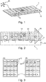
Fig. 1 is a schematic perspective view of an embodiment of a nanoparticle screening chip; -
Fig. 2 is a schematic section across a further embodiment of a nanoparticle screening chip during feeding with a nanoparticle containing fluid; -
Fig. 3 is a schematic representation of a further embodiment of a nanoparticle screening chip showing a plurality of areas (noted A01, ... inFig. 3(A) ) with different dispersive, Acid-Base and charge properties, and within each of said areas are located subareas with different hole sizes (shown as three rectangles inside areas A01, A02 and A03, although not represented, each other of the areas preferably have the same or equivalent subareas); -
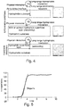
Fig. 4 is a schematic representation of unfavorable conditions preventing hydrophobic nanoparticles to bind to a hydrophobic surface, as well as a way to make these conditions more favorable. -
Fig. 5 is a diagram showing the kinetics of the binding of nanoparticles to a surface, the slope s (straight line) of the curve being proportional to the surface free energy balance ΔGadh. -
Fig. 6 are two SEM photographs of 200 nm nanoparticles, once on a substrate having grooves of 300 nm aperture (A) and once on a substrate having grooves of 100 nm aperture (B). -
Fig. 7 is a schematic setup of a reading device useable for implementing a method as described herein in particular with a nanoparticle screening chip of the invention. - Further details and advantages of the present invention will be apparent from the following detailed description of several not limiting embodiments with reference to the attached drawings.
- As depicted in
Fig. 1 - 3 , the method preferably uses a screening chip 1 (also called sensing chip) comprising an opticallyreflective substrate 10 with a (working)surface 11 provided withareas 12 having different surface properties. - As schematically represented in
Fig. 1 and 3 , eacharea 12 is characterised by given values of the surface free energy components, the Total Free Energy of a solid surface being defined as:
- γLW = dispersive (Lifshitz-van der Waals) component = d
- γ+ = electron acceptor component = b
- γ- = electron donor component = a
- Each
single area 12 of the surface can thus be defined by the three components (also called triplet) (d,b,a). Thesurface 11 of the sensing chip 1 can thus be characterised by a plurality ofareas 12 and each of them presents different surface properties i.e. surface energy component (d,b,a). - Hence,
NMs 20 in suspension or in a colloidal solution are characterised by the equivalent triplets of values of the surface energy according to their surface properties. - So, a triplet (d,b,a) can be defined for any given NM, (d,b,a)NMs.
- As shown in
Fig. 2 ,NMs 20 flowing (as indicated by horizontal arrow 30) along the sensing chip'ssurface 11 by means e.g. of a liquid cell will be attracted (illustrated by arrows pointing to surface 11) by the respective areas A = A(d,b,a) according to their surface properties (d,b,a)NMs. NMs having different surface properties will not be attracted or even be repulsed (arrows pointing away from surface 11) and thus stay within the liquid until they reach an area corresponding to their surface properties (d,b,a)NMs. - By this method, the (d,b,a) triplet of the NMs will be reconstructed according to the affinity of the NMs to the different areas with the corresponding surface properties.
- Furthermore, each
area 12 on the sensor chip is composed of different smaller areas (subareas 13) as shown inFig. 3(B) characterised by an array of sub-micrometric holes orgrooves 15. Eachsubarea 13 is characterized by holes orgrooves 15 with different aperture sizes, S, such as S1, S2, S3, ..., Sn. - Each
subarea 13 is characterised by a particular optical response, when illuminated by a beam of visible light at a certain angle of incidence and polarization. As a result of the nanograting, the incident light is diffracted at a given wavelength as a function of the refractive index of the hole or groove 15 containing or not the NMs. The presence ofNMs 20 in the holes orgrooves 15 can be thus monitored by measuring the wavelength of the diffracted light. - Hence,
NMs 20 during their transport along thesurface 11 of the chip 1 are attracted (or not) by hydrophobic or other forces towards the surface. Among the attracted NMs, only those with a diameter smaller than the aperture size of the holes S will be captured within the holes orgrooves 15. NMs captured within the holes will locally change the refractive index of the nanoholes and modify the optical response of the grating. By monitoring the optical response, the presence of NMs with a diameter smaller than a certain size Smin (hole size) are detectable. - The optical reader preferably consists of a microscope in dark field (DF) configuration, in particular with a CCD camera enabling to capture and to measure the reflection image of the whole sensing surface.
- The optical reader is characterised by a certain Field of View (FoV) and a Numerical Aperture (NA). The NA determines the angle of incidence of the detection light beam. For a given NA, flat areas (non-structured, without diffraction grating) will not reflect light and will appear black to the detector. On the contrary, areas with the diffraction grating will be reflected at a given wavelength, function of the geometrical parameter of the grating and the refractive index of the holes (with or without presence of NMs).
- When NMs fill the holes of the grating the reflected colour of the area will change accordingly, so the presence of NMs in the holes can be by monitored by colour changes visually or with a camera sensor.
- In another aspect, the invention in particular relates to the sensing chip (nanoparticle screening chip) having the features as described herein.
- According to the inventors, the main advantage of the invention is that the proposed solution enables the rapid screening of samples containing NMs. Indeed, the sensor will enable the detection within a few seconds (and with very limited sample amount, such as few hundreds of µl) the presence of NMs smaller than size Smin. Furthermore, the use of different Smin within one subarea and hence the presence and proportion of NMs within one or more of the differently sized holes will provide information about NM size distribution. Together with the minimum size, the device will allow to characterise the surface property of the NMs, determining their acidic, basic or dispersive components, as well as their sizes and size distributions.
- Below are described some experiments and considerations done in the context of making the present invention. These experiments provide further guidance for the skilled person in order to reduce to practice the present invention. The information below should however not be construed as limiting the invention to the particular embodiments and results described.
- A silicon substrate (it might be glass or any other flat surface) was modified by different plasma deposition in order to tune the surface hydrophobicity. Polytetrafluoroethylene was used to generate a hydrophobic surface, the deposition was realized using pure octofluorocyclobutane (C4F8) as the gas precursor at a pressure of 3.2 Pa (27 mTorr), applying a power of 142 W for 5 min. Plasma-polymerized acrylic acid was deposited as a hydrophilic surface, using acrylic acid as the gas precursor at a pressure of 2.1 Pa (16 mTorr), applying a bias power of 400 W for 5 min.
- In order to tune the surface hydrophobicity, a layer-by-layer deposition of two polyelectrolytes was realized. The plasma-modified substrates were incubated for 2 min in Poly(diallyldimethylammonium chloride) (PDDA) 2% solution in water or in Poly(sodium 4-styrene sulfonate) (PSS) 2% in water for the self-assembly deposition of each polyelectrolyte layer-by-layer, starting from PDDA (positively charged) and alternating with PSS (negatively charged). After each step, the substrate was rinsed with milliQ water and dried under nitrogen flow.
- A first study was realized using 200 nm diameter polystyrene particles (Polybead® microspheres, Polysciences). Those commercial particles were chosen as a model because of the large range of sizes and surface functionalization (corresponding to different hydrophobicity and charges) offered by the provider. The non-modified particles are stabilized by sulfonate groups; they are negatively charged and hydrophobic.
- The modified surfaces were incubated with the model particles in order to evaluate the binding, associated to the interaction forces between the particles and the surfaces. The experiment was realized using 16 different conditions of salt concentration ([NaCl] = 0 / 1 / 10 / 100 mM) and pH (2 / 4 / 7 / 10) in aqueous solution in which the particles were dispersed at the original concentration. The incubation took place with the substrate fully immersed in the different solutions for 30 min, then rinsed thoroughly with milliQ water and dried under nitrogen flow. The surfaces were finally imaged with Scanning Electron Microscopy (SEM).
- The same experiment was realized with polystyrene particles modified with hydroxyl groups. This surface modification conferred to the particles a higher hydrophilicity.
- In order to study the selective binding of NPs on chemically modified surfaces, two set of samples have been prepared. A first set of Silicon samples had been coated first with a plasma deposited layer of PTFE and then several layers of polyelectrolyte (PPS/PDDA) for decreasing the hydrophobicity level. A second set of sample has been prepared with a starting layer of PAA. Theses samples have been modified as well with PE deposition to decrease the surface hydrophobicity.
- The results of characterization are presented in Tables 1 and 2.
Table 1: Summary of the characterization of the PTFE modified surface Contact angle (°) Ellipsometry Height (nm) AFM Roughness (nm) Z-potential at pH 7 PSS #3 19.8 ± 0.4 0.65 ± 0.01 0.76 ± 0.08 -57.64 ± 0.31 PDDA #3 37.4 ±0.3 0.44 ± 0.01 0.85 ± 0.09 -4.13 ± 0.33 PSS #2 53.3 ± 0.8 0.69 ± 0.01 0.83 ± 0.08 -62.37 ± 0.59 PDDA #2 65.4 ± 0.6 1.11 ± 0.02 0.85 ± 0.09 -4.93 ± 0.25 PSS #1 64.6 ± 0.7 0.66 ± 0.01 0.48 ± 0.05 -60.22 ± 0.90 PDDA #1 79.3 ± 0.7 1.43 ± 0.02 0.45 ± 0.05 -26.28 ± 0.24 PTFE 106.8 ±0.4 0.29 ± 0.03 -61.18 ± 0.13 Table 2: Summary of the characterization of the PAA modified surface Contact angle (°) Ellipsometry Height (nm) AFM Roughness (nm) Z-potential at pH 7 PSS #3 22.8 ± 0.4 0.65 ± 0.01 1.87 ± 0.19 -62.60 ± 0.33 PDDA #3 28.2 ± 0.6 0.44 ± 0.01 1.88 ± 0.19 -6.53 ± 0.68 PSS #2 25.2 ± 0.1 0.69 ± 0.01 1.09 ± 0.11 -50.37 ± 0.92 PDDA #2 30.9 ± 0.4 1.11 ± 0.02 0.77 ± 0.08 2.80 ± 0.15 PSS#1 41.4 ± 0.8 0.66 ± 0.01 0.65 ± 0.07 -47.36 ± 0.29 PDDA #1 52.1 ± 0.5 1.43 ± 0.02 0.12 ± 0.01 -5.04 ± 0.53 PAA 58.3 ± 0.5 0.23 ± 0.02 -78.12 ± 1.38 - As shown in Table 1, the sample coated with PTFE plasma-deposited layer was highly hydrophobic, with a contact angle of 106°. For each polyelectrolyte layer the contact angle measurement showed a decrease in the hydrophobicity of the surface, from 80° (hydrophobic) for the first layer, to 20° (highly hydrophilic) for the 6th layer. The ellipsometry (optical technique for investigating the dielectric properties of thin films) enabled to measure the thickness of each polyelectrolyte layer. The PSS layers were around 0.7 nm thick, and each PDDA between 1.4 and 0.4 nm, the first one being the thickest. The AFM provided information on roughness that was increasing with the first 3 layers from 0.3 to 0.8 before being stable around 0.8 nm for the last 3 layers. The z-potential was measured for different pH, for all layers a negative z-potential was obtained for the whole range of pH, especially for the PTFE non-modified and the PSS layers, and closer to neutral for the different PDDA layers. This result can be explained knowing that the PDDA is positively charged and the PDDA and PTFE negatively charged.
- The experiments performed on the PAA modified surface (Table 2) showed the same trend. With a base layer of PAA more hydrophilic, one could indeed reach the same surface properties with an increase in hydrophilicity with the polyelectrolytes layers, a more important increase in roughness and a zeta-potential negative for all conditions. The 6th layer enabled to obtain close surface properties with two substrates of different properties, PTFE or PAA.
- The XPS and ToF-SIMS analysis of the surface modifications by PTFE plasma deposition and layer-by-layer polyelectrolytes deposition was also performed (data not shown). The surface analysis through XPS experiments demonstrated the presence of the PTFE on the silicon substrate, and the ToF-SIMS experiment confirmed those observations, with an analysis that is more surface sensitive, the coverage of the silicon substrate with the PTFE plasma, and of the PTFE base layer with the 6 layers of polyelectrolytes.
- Considering that the silicon substrates modified by plasma deposition of PTFE shows a high hydrophobicity, a first experiment was performed with hydrophobic particles in different conditions. The PS particles in 16 conditions of pH and ionic strength were incubated on the surface in order to evaluate the binding of hydrophobic particles with a hydrophobic surface, expected to be high because of the hydrophobic forces. The surfaces were then analyzed with SEM and the ratio of the surface coverage was calculated for the different conditions using ImageJ software. Those results are presented in Table 3.
Table 3. Surface coverage (%) of PS particles on PTFE, contact angle = 105° pH 2 4 7 10 Z-potential 3 -32 -54 -140 [NaCl] mM 0 2.5 2.4 0.8 0.6 1 2.1 0.2 0.1 0.9 10 5.6 6.6 0.1 0.0 100 2.5 27.0 2.8 0.3 - Surprisingly, the binding rate was low for all conditions, with a slight trend to a higher binding for low pH and high salt concentration.
- The low binding of NP on the hydrophobic PTFE surface was hypothetically attributed to the poor wettability of the PTFE surface with the creation of micro-bubbles, which impede the contact between the surface and the particles in the water suspension, preventing the hydrophobic forces to take place.
- The negative charges at the surface of the PTFE layer and of the particles would indeed be decreased for low pH and high ionic strength, in those conditions the long range repulsion by electrostatic forces would then be drastically decreased, enabling the shorter range hydrophobic forces to take place.
- The following hypothesis is proposed to understand the low binding for all conditions. The interface between the surface and the particles should be considered as multiple interfaces: since the particles are incubated in an aqueous solution, the water is playing an important role into the substrate-particles interaction with a substrate-water interface and another interface particles-water. The exposition of the highly hydrophobic substrate to water would generate micro-air bubbles to limit the contact, and the same would happen on the surface of the hydrophobic particles. Those micro-bubbles could create a physical barrier, preventing the particles to approach to the surface close enough for the hydrophobic interactions to take place. To limit the presence of those air bubbles enabling the water contact on the surface, the hydrophobicity should then be decreased.
- In order to verify this hypothesis, the same experiments were performed with the PTFE surface modified with polyelectrolyte layers. Since the number of polyelectrolyte layers has a direct influence on the hydrophobicity (as seen with the contact angle measurements), it was possible to achieve four different degree of hydrophobicity, corresponding to contact angles of 105°, 70°, 50° and 20°. The observation of the surfaces after incubation of the particles showed a progressive increase of the binding, with a more and more important surface coverage of the surface for a decreasing contact angle. The calculated surface coverage by the particles for the lowest contact angle is presented in Table 4.
Table 4: Surface coverage of PS particles on PTFE+PE (6 layers), contact angle = 20° pH 2 4 7 10 Z-potential -3 -49 -60 -100 [NaCl] mM 0 54.2 57.2 33.0 3.6 1 40.4 37.8 30.5 30.9 10 49.2 43.4 48.0 47.6 100 83.3 64.3 55.1 51.5 - Compared to the results without polyelectrolytes, the surface coverage by the particles is dramatically increased with the 6 polyelectrolytes layers. Moreover, the trend already observed is confirmed, with an important increase of the binding with the decrease in pH and the increase of ionic strength. To compare the binding rate obtained on a hydrophobic substrate + hydrophilic superficial layer with the binding rate on a hydrophilic substrate and to verify the theory of the long range interactions, another experiment was performed using the previously described plasma deposited PAA, with and without the polyelectrolyte modification. The degree of hydrophobicity was tuned from around 60° of contact angle without polyelectrolyte to 20° with six layers of polyelectrolytes. The different surfaces after incubation of hydrophobic polystyrene particles in the same conditions as before were observed by SEM and the results in terms of surface coverage is presented in Table 5 for PAA alone (a) and PAA with six layers of polyelectrolytes (b).
Table 5: Surface coverage of PS particles on a. PAA, b. PAA + PE pH 2 4 7 10 a. PAA Z-potential -26 -45 -78 -83 [NaCl] mM 0 0,0 3,4 0,0 0,0 1 0,9 0,1 0,0 0,0 10 0,1 0,2 1,8 0,0 100 80,8 51,6 39,4 0,4 b. PAA + PE Z-potential -20 -50 -63 -53 [NaCl] mM 0 1,0 0,0 0,0 0,0 1 43,1 0,0 0,0 0,0 10 32,0 0,6 0,0 0,1 100 59,3 54,2 19,9 27,5 - As can be observed for both PAA alone and PAA + PE, the surface coverage is extremely low for most of the conditions, with salt concentration between 0 and 10, and all pH on PAA alone and
pH 4 to 10 on PAA + PE. The trend already observed before is still present with an increase of the binding rate with the increase of ionic strength and the decrease of pH, but even more than before since the particles binding increases only in those extreme conditions. Comparing the results on the PAA and PTFE substrates without polyelectrolytes (Table 3 and 5a), it can be assumed that, with the highest ionic strength, the binding is more important on PAA than on PTFE because of the physical barrier existing because of the highly hydrophobic properties of the PTFE. But, the main difference appears to be between PTFE + PE and PAA + PE (Table 4 and 5b). Indeed, adding the polyelectrolytes layers induce a large increase in the binding on the hydrophobic substrate, whereas the change with polyelectrolyte on PAA is significant only forpH 2 with salt, showing that the hydrophilic superficial layer only permit the hydrophobic interactions to take place, resulting in the binding of the hydrophobic particles only on the hydrophobic substrate. - A schematic interaction model of the long-range hydrophobic forces and the effect of the hydrophobicity of the substrate is presented in
Fig. 4 . - As presented in
Fig. 4 showing the theoretical model of interactions according to different conditions, in the first tested case, the hydrophobic PTFE was in direct contact with the aqueous medium containing the particles. In this condition an air interface is generated to limit the contacts between water and the hydrophilic substrate, and this prevents the physical interaction between the particles and the substrate. In addition, if the electrostatic repulsion is not avoided through a decrease of pH and/or an increase of ionic strength, the hydrophobic interactions acting at shorter range can't take place. On the contrary, by minimizing the electrostatic repulsion thanks to low pH and high salt concentration, and enabling the physical interaction through the use of a superficial hydrophilic layer in top of the hydrophobic substrate, the most favorable conditions can be obtained for the binding of hydrophobic particles on the hydrophobic substrate. The hydrophilic layer has to be thin enough (<< 100nm) in order for the hydrophobic interactions to take place at the long range. The use of a polyelectrolyte layer is in this case a good way to obtain a high hydrophilicity with a thin coverage of the hydrophobic substrate. The superficial hydrophobicity/ hydrophilicity degree, also called wettability, is therefore not driving the binding but enables the hydrophobic interactions to take place. - The second part of the study consisted in the evaluation of the binding of hydrophilic particles on the previously used substrates. Considering that the system mechanism is based on hydrophobic interactions, its interest would be to enable to characterize the particles hydrophobicity thanks to different binding response on the patterned areas. The particles used for this part of the study were the same polystyrene particles but modified with hydroxyl groups which give them hydrophilic properties.
- The PS-OH particles in 16 conditions of pH and ionic strength were incubated on the different surfaces. The analysis by SEM enabled then to calculate the ratio of the surface coverage for the different conditions. The results obtained on PTFE, PTFE + PE, PAA and PAA + PE are presented in Table 6.
Table 6: Surface coverage of PS-OH particles on a. PTFE, b. PTFE+PE, c. PAA, d. PAA+ PE pH 2 4 7 10 a. PTFE [NaCl] mM 0 0.0 0.2 0.0 0.0 1 0.0 0.0 0.0 0.0 10 6.9 0.0 0.0 0.0 100 0.0 0.6 4.0 0.0 b. PTFE + PE [NaCl] mM 0 0.3 0.2 0.0 0.0 1 0.9 0.4 0.0 0.2 10 0.6 0.7 0.1 0.1 100 2.6 10.2 1.9 6.5 c. PAA [NaCl] mM 0 0.2 0.0 0.0 0.0 1 0.8 0.5 0.0 0.0 10 0.2 0.1 0.1 0.0 100 36.5 51.7 22.2 1.6 d. PAA + PE [NaCl] mM 0 0.3 0.0 0.0 0.0 1 0.3 0.0 0.0 0.0 10 2.3 0.1 0.0 0.0 100 54.0 37.8 1.0 1.4 - As can be seen, the hydrophilic particles have a binding rate extremely low (<1% in most of the cases) for all conditions on the hydrophobic substrate, modified or not. On the hydrophilic substrate, modified with the polyelectrolytes or not, there is no binding in most of the conditions, with a significant binding only for high salt concentration and negative pH as already observed before. Those results confirm what was expected, with no hydrophobic interactions the hydrophilic particles did not bind to the different surfaces.
- The generic method for the determination of the surface energy of an unknown sample of nanoparticles is similar to the extended DLVO model (Van Oss et al., J. Colloid Interface Sci. 111, 378-390).
- When a nanoparticle in solution (many nanoparticles) gets in close contact with a surface there are different forces attracting or repelling the NP to/from the surface
- The forces are according

- With FLW : Lifshitz-Van der Waals interaction force (attractive, short range)
- FEL : Electrostatic interaction force (attractive or repulsive, long range)
- FAB : Acid-base interaction force (hydrophobic interaction)
- The Lifshitz-Van der Waals component is always attractive and always present.
- The Electrostatic component can be attractive or repulsive, but anyway can be totally screened by the increase of the salt concentration. In any case, its values are known from the measurement of the Zeta potentials of the nanoparticles and the chip active surfaces. Between two surfaces with the same charge they are repulsive.
- The AB forces include the hydrophobic interaction.
- If one assumes that the attraction forces are ONLY the AB forces, they are long-range (acting when the NP is at several nm from the surface) and they are strong (this is controlled by the present experimental conditions).
- The NPs are attracted to the surface and they stay there only if they are in a situation that minimizes the surface free energy of the system surface-liquid-NP. By definition:
l: liquid n: nanoparticle s: substrate - Interfacial free energies:
- γsl KNOWN
- γsn MEASURED
- γnl TO BE DETERMINED
- Free energy of adhesion ΔGadh = γnl - γsn - γsl
- The surface free energy balance (ΔGadh) is the balance between the interfacial energies (of the NP and the surface) with the liquid and the interface of the NP and the surface.
- The present goal is to calculate the γnl (the surface energy component of the NP, in particular the LW-hydrophobic component).
- The geometric relationship between the surface components can be expressed as follows:


- With the presented system, the ΔGadh can be measured directly by measuring the kinetics of adsorption the nanoparticles on the surface. In particular ΔGadh is proportional to the slope s of the kinetics of adsorption (see
Fig. 5 ). - Hence, a preferred determination step of a method of the invention could be summarized as follows:
- (a) One measures and one knows the surface properties of each surface
- (b) One measures the kinetics of adsorption of the NP on each surface
- (c) One calculates the surface properties of the NP.
- The areas characterized by controlled surface properties (as explained above) can be micro-patterned on a same surface e.g. by the following microfluidic device (MFD) designed by the inventors.
- 1) The surface of the chip can be modified by PTFE or PAA or any other polymer with controlled hydrophobicity/hydrophilicity,
- 2) The MFD is applied on top of the chip,
- 3) In each area of the MFD is flown as certain number of polyelectrolytes layers in order to locally modify the surface properties.
- The physical filters or capturing structures for the nanoparticles (holes arrays or grooves arrays) are nanofabricated on the surface of the chip e.g. by Ion Beam Milling, but the same structure can be made using different fabrication techniques.
- The basic purpose is:
- 1) to create a diffraction grating (made of holes or grooves)
- 2) The same diffraction grating is filtering the NP
- 3) Only the NP smaller than the grating size can fall inside the grating
- 4) The optical response of the diffraction grating changes only when NP are located inside the grooves
- 5) In this way, particles smaller than a chosen size can easily be detected.
- Grating 1 which has lines (grooves) of 300 nm wide is fed with 200 nm nanoparticles,
-
Grating 2 which has lines of 100 nm wide is fed with 200 nm NP,
It is clear that 200 nm NP will fall inside the 300 nm grooves, while they stay on top of the 100 nm grooves (SeeFig. 6(A) and (B) which are SEM images of Polystyrene NP on a hydrophobic surface) - 1) The optical response of the diffraction spectrum of the Grating 1 is modified by the presence of the NP in the grooves (
Fig. 6(A) ) - 2) The optical response of the diffraction spectrum of the
Grating 2 is modified by the presence of the NP on top of the grooves (Fig. 6(B) ) - The changes in the optical response can be following in real time during the NP adsorption and the kinetics curve can be reconstructed to calculate ΔGadh (see above and
Fig. 5 ). Moreover, it is possible to do a fast screening of the NP size. - A preferred system to analyze the NP on the screening chip basically comprises of a dark field microscope with a large Field-of-view (to detect all the areas of the chip at the same time), which allows detecting NPs inside or outside the diffraction gratings and wherein the detection may be done in real time.
- An example is shown in
Fig. 7 , wherein alight source 41 emits light passing through afirst lens system 42, reflected bybeam splitter 43 throughillumination pupil 44 and asecond lens system 45 onto thenanoparticle screening chip 46. The light which is refracted by thescreening chip 46 passes throughillumination pupil 44,splitter 43 and athird lens system 47 through theaperture 48 of acamera 49. - As an example, such a system may comprise:
from Edmund Optics / Thorlabs: - two Erfle eyepieces 41-347 as
lens systems - 50mm beamsplitter cube 32-704 as
beam splitter 43 - 3-4 PCX (or achromatic pairs) lenses and lens mounting system (cage etc.) for
lens system 47 - As there is a common path for imaging and illumination between
screening chip 46 andbeam splitter 43, there may be some reflections to the image. In fact, the illumination angle can be adjusted by moving the hole plate inillumination pupil 44. -
- 1
- Nanoparticle screening chip
- 10
- Substrate
- 11
- Working surface
- 12
- Areas
- 13
- Subareas
- 15
- Submicronic hole or groove
- 20
- Nanoparticle(s)
- 30
- Liquid flow
- 40
- Dark field detection setup
- 41
- Light source
- 42
- First lens system
- 43
- Beam splitter
- 44
- Illumination pupil
- 45
- Second lens system
- 46
- Sample/screening chip
- 47
- Third lens system
- 48
- Imaging NA adjustment from camera lens
- 49
- Camera
Claims (15)
- A nanoparticle screening chip (1) allowing for determining physical properties of nanoparticles (20), wherein the screening chip comprises a substrate (10) having a working surface (11) divided into a plurality of areas (12), wherein(1) each of these areas (12) presents different surface properties defined by surface energy component (d,b,a), the total free energy γTOT of the surface of each area being defined as follows:
 γLW = dispersive component = dγ+ = electron acceptor component = bγ- = electron donor component = aand(2) each of these areas (12) comprises a plurality of subareas (13), each subarea comprising an array of sub-micrometric holes or elongated grooves (15) with a different aperture size (S1, S2, S3, ...).
 - The nanoparticle screening chip (1) according to claim 1, wherein the number of areas (12) is from 5 to 100, preferably from 10 to 50.
- The nanoparticle screening chip according to claim 1 or 2, wherein the number of subareas (13) is from 2 to 10, preferably from 3 to 6.
- The nanoparticle screening chip (1) according to any of claims 1 to 3, wherein the substrate (10) is a highly flat substrate, preferably selected from glass or silicon.
- The nanoparticle screening chip (1) according to any of claims 1 to 4, wherein a one dimensional dielectric mirror or a noble metal, preferably gold, has been deposited on the substrate (10).
- The nanoparticle screening chip (1) according to any of claims 1 to 5, wherein the surface properties of at least one area have been modified by plasma deposition of one or more layers of at least one optionally functionalized polymer, such as polytetrafluoroethylene, polyethylene oxide or poly(acrylic acid).
- The nanoparticle screening chip (1) according to claim 6, wherein the surface properties of the substrate (10) have been further modified by using self-assembly of polyelectrolytes, such as poly(diallyldimethylammonium chloride) and/or poly(sodium 4styrene sulfonate).
- The nanoparticle screening chip (1) according to any of claims 1 to 7, wherein a number of said areas (12) presenting different surface properties comprise one or more hydrophobic layer(s) with a superficial hydrophilic layer to increase hydrophobicity.
- A method for screening nanoparticles to determining physical properties thereof, the method comprising the steps of(a) feeding nanoparticles in solution/suspension over the working surface (11) of a nanoparticle screening chip (1) according to any of claims 1 to 8,(b) incubating the nanoparticles in solution over the working surface (11) during an incubation time t and thereafter rinsing the nanoparticle screening chip (1),(c) determining physical properties of the nanoparticles by analyzing the nanoparticle screening chip (1) by optical microscopy.
- The method according to claim 9, wherein in step (b) the incubation time t is between 2 seconds and 60 minutes, preferably between 5 seconds and 45 minutes.
- The method according to claim 9 or 10, wherein in step (a) and/or in step (b), pH and/or salt concentration of the nanoparticles containing solution or suspension is adjusted.
- The method according to any of claims 9 to 11, wherein the determination of the physical properties of the nanoparticles further comprises the calculation of the surface properties of the nanoparticles by determining the surface free energy balance, including the electrostatic interactions and in particular the two surface energy components:


- The method according to any of claims 9 to 12, wherein in step (c) the nanoparticle screening chip (1) is inserted in a reading device allowing for optically determining the presence and the location of nanoparticles within the areas (12) and subareas (13) of working surface (11), wherein the reading device comprising a light source (41), a holding port arranged for holding said nanoparticle screening chip (1) in front of said light source and a microscope enabling to measure the reflection image of the working surface (11), preferably said microscope is a dark field microscope, more preferably integrating a CCD camera.
- A nanoparticle screening chip reading device, configured to optically determine the presence and further physical properties of nanoparticles on a nanoparticle screening chip (1) according to any of claims 1 to 8, comprising a light source (41), a holding port arranged for holding said nanoparticle screening chip relative to said light source, a light detector and/or an imaging device, in particular a microscope capable of measuring a reflection image of the whole working surface (11), preferably said microscope has a dark field configuration, more preferably in combination with a CCD camera.
- Use of a nanoparticle screening chip (1) according to any of claims 1 to 8, of a nanoparticle screening chip reading device according to claim 14 or of a method according to any of claims 9 to 13 for quality control in industrial manufacturing processes, especially in nanomedicine.
Applications Claiming Priority (2)
| Application Number | Priority Date | Filing Date | Title |
|---|---|---|---|
| EP15166302.8A EP3091347A1 (en) | 2015-05-04 | 2015-05-04 | Screening of nanoparticle properties |
| PCT/EP2016/059633 WO2016177641A1 (en) | 2015-05-04 | 2016-04-29 | Screening of nanoparticle properties |
Publications (3)
| Publication Number | Publication Date |
|---|---|
| EP3292391A1 EP3292391A1 (en) | 2018-03-14 |
| EP3292391B1 true EP3292391B1 (en) | 2019-06-05 |
| EP3292391B8 EP3292391B8 (en) | 2019-07-17 |
Family
ID=53039789
Family Applications (2)
| Application Number | Title | Priority Date | Filing Date |
|---|---|---|---|
| EP15166302.8A Withdrawn EP3091347A1 (en) | 2015-05-04 | 2015-05-04 | Screening of nanoparticle properties |
| EP16721127.5A Active EP3292391B8 (en) | 2015-05-04 | 2016-04-29 | Screening of nanoparticle properties |
Family Applications Before (1)
| Application Number | Title | Priority Date | Filing Date |
|---|---|---|---|
| EP15166302.8A Withdrawn EP3091347A1 (en) | 2015-05-04 | 2015-05-04 | Screening of nanoparticle properties |
Country Status (10)
| Country | Link |
|---|---|
| US (1) | US10408727B2 (en) |
| EP (2) | EP3091347A1 (en) |
| JP (1) | JP6684827B2 (en) |
| CN (1) | CN107709966B (en) |
| AU (1) | AU2016257244B2 (en) |
| BR (1) | BR112017023759B1 (en) |
| CA (1) | CA2984581C (en) |
| ES (1) | ES2737726T3 (en) |
| HK (1) | HK1251652B (en) |
| WO (1) | WO2016177641A1 (en) |
Families Citing this family (2)
| Publication number | Priority date | Publication date | Assignee | Title |
|---|---|---|---|---|
| TWI912371B (en) * | 2021-01-14 | 2026-01-21 | 瑞士商通用表面增強光譜學股份有限公司 | A method for determining the size of particles and an assembly therefor |
| CN116008126B (en) * | 2022-12-29 | 2026-01-09 | 暨南大学 | A method for determining the critical hydrochemical conditions for the aggregation and deposition of biochar nanoparticles |
Family Cites Families (21)
| Publication number | Priority date | Publication date | Assignee | Title |
|---|---|---|---|---|
| JPS60163901A (en) * | 1984-02-04 | 1985-08-26 | Japan Synthetic Rubber Co Ltd | Plasma polymerization treatment method |
| IL126544A (en) * | 1996-04-25 | 2004-08-31 | Genicon Sciences Inc | Analyte assay using scattered-light detectable particles |
| US7264973B2 (en) * | 2000-10-30 | 2007-09-04 | Sru Biosystems, Inc. | Label-free methods for performing assays using a colorimetric resonant optical biosensor |
| JP2003057173A (en) * | 2001-08-09 | 2003-02-26 | Mitsubishi Chemicals Corp | Sample analysis method and analyzer using surface plasmon resonance, and surface plasmon resonance sensor chip |
| TW200304385A (en) * | 2002-03-13 | 2003-10-01 | Novartis Ag | Materials containing multiple layers of vesicles |
| US20050084980A1 (en) * | 2003-10-17 | 2005-04-21 | Intel Corporation | Method and device for detecting a small number of molecules using surface-enhanced coherant anti-stokes raman spectroscopy |
| JP2005152849A (en) * | 2003-11-27 | 2005-06-16 | Kitakyushu Foundation For The Advancement Of Industry Science & Technology | Floating particulate collection filter, suspended particulate collection method using the same, suspended particulate analysis method, and suspended particulate collection apparatus |
| JP4375576B2 (en) * | 2004-08-30 | 2009-12-02 | 株式会社島津製作所 | Optical measuring apparatus and method, and nanoparticle measuring method and apparatus |
| WO2006098772A2 (en) * | 2004-10-13 | 2006-09-21 | U.S. Genomics, Inc. | Systems and methods for measurement optimization |
| JP4117665B2 (en) * | 2005-03-03 | 2008-07-16 | 独立行政法人物質・材料研究機構 | Optical analysis chip and manufacturing method thereof, optical analysis device, and optical analysis method |
| US7752931B2 (en) * | 2005-11-03 | 2010-07-13 | University Of Massachusetts | Nanopatterned surfaces and related methods for selective adhesion, sensing and separation |
| DE102006029032A1 (en) * | 2006-02-17 | 2007-08-23 | Poly-An Gesellschaft zur Herstellung von Polymeren für spezielle Anwendungen und Analytik mbH | Apparatus, method and kit for detecting analytes in a sample |
| US7842352B2 (en) * | 2006-08-09 | 2010-11-30 | Massachusetts Institute Of Technology | Nanoparticle coatings and methods of making |
| US7993525B2 (en) * | 2006-12-29 | 2011-08-09 | Intel Corporation | Device and method for particle complex handling |
| WO2009002386A2 (en) * | 2007-05-24 | 2008-12-31 | The Regents Of The University Of Californina | Size-dependent biological effect of nanoparticles |
| WO2008152712A1 (en) * | 2007-06-13 | 2008-12-18 | Shimadzu Corporation | Nanoparticle measuring instrument |
| US8283936B2 (en) * | 2009-02-09 | 2012-10-09 | Board Of Regents, The University Of Texas System | Nano-scale biosensors |
| SE535087C2 (en) * | 2010-08-24 | 2012-04-10 | A method of preparing a flat surface with a controlled density gradient of deposited nanoparticle particles | |
| US10794904B2 (en) * | 2013-03-15 | 2020-10-06 | Nicoya Lifesciences Inc. | Self-referencing sensor for chemical detection |
| WO2016036409A1 (en) * | 2014-09-05 | 2016-03-10 | California Institute Of Technology | Surface enhanced raman spectroscopy detection of gases, particles and liquids through nanopillar structures |
| CN104568684B (en) * | 2015-01-30 | 2017-06-27 | 中国科学院重庆绿色智能技术研究院 | A kind of nano particle detecting system and screening assays |
-
2015
- 2015-05-04 EP EP15166302.8A patent/EP3091347A1/en not_active Withdrawn
-
2016
- 2016-04-29 WO PCT/EP2016/059633 patent/WO2016177641A1/en not_active Ceased
- 2016-04-29 CN CN201680038727.6A patent/CN107709966B/en active Active
- 2016-04-29 HK HK18110968.7A patent/HK1251652B/en unknown
- 2016-04-29 CA CA2984581A patent/CA2984581C/en active Active
- 2016-04-29 JP JP2017557926A patent/JP6684827B2/en active Active
- 2016-04-29 BR BR112017023759-8A patent/BR112017023759B1/en active IP Right Grant
- 2016-04-29 EP EP16721127.5A patent/EP3292391B8/en active Active
- 2016-04-29 ES ES16721127T patent/ES2737726T3/en active Active
- 2016-04-29 AU AU2016257244A patent/AU2016257244B2/en active Active
- 2016-04-29 US US15/571,808 patent/US10408727B2/en active Active
Non-Patent Citations (1)
| Title |
|---|
| None * |
Also Published As
| Publication number | Publication date |
|---|---|
| CA2984581A1 (en) | 2016-11-10 |
| CN107709966A (en) | 2018-02-16 |
| US10408727B2 (en) | 2019-09-10 |
| HK1251652B (en) | 2020-05-15 |
| EP3091347A1 (en) | 2016-11-09 |
| EP3292391B8 (en) | 2019-07-17 |
| US20180266932A1 (en) | 2018-09-20 |
| CA2984581C (en) | 2022-03-15 |
| JP2018524555A (en) | 2018-08-30 |
| ES2737726T3 (en) | 2020-01-15 |
| EP3292391A1 (en) | 2018-03-14 |
| WO2016177641A1 (en) | 2016-11-10 |
| CN107709966B (en) | 2020-04-24 |
| WO2016177641A9 (en) | 2016-12-29 |
| JP6684827B2 (en) | 2020-04-22 |
| HK1251652A1 (en) | 2019-02-01 |
| AU2016257244B2 (en) | 2021-01-28 |
| BR112017023759A2 (en) | 2018-07-31 |
| BR112017023759B1 (en) | 2021-06-29 |
| AU2016257244A1 (en) | 2017-12-07 |
Similar Documents
| Publication | Publication Date | Title |
|---|---|---|
| Wang et al. | Holographic characterization of colloidal fractal aggregates | |
| Kim et al. | Microfluidic designing microgels containing highly concentrated gold nanoparticles for SERS analysis of complex fluids | |
| EP2233923B1 (en) | Method and apparatus for the characterisation of the coagulation dynamics or sedimentation of blood or blood serum | |
| Kadunc et al. | In-line monitoring of pellet coating thickness growth by means of visual imaging | |
| US20070229823A1 (en) | Determination of the number concentration and particle size distribution of nanoparticles using dark-field microscopy | |
| CN108369170B (en) | Method for determining the mean radius of gyration of particles of a size ≤ 1 μm in suspension and equipment for carrying out the method | |
| CN106461571A (en) | Method for particle detection on flexible substrates | |
| US10408727B2 (en) | Screening of nanoparticle properties | |
| Cavicchi et al. | Particle shape effects on subvisible particle sizing measurements | |
| WO2018005687A1 (en) | Method for calibrating investigated volume for light sheet based nanoparticle tracking and counting apparatus | |
| Qu et al. | Asymmetric flow field flow fractionation for the characterization of globule size distribution in complex formulations: a cyclosporine ophthalmic emulsion case | |
| Haiden et al. | Sizing of metallic nanoparticles confined to a microfluidic film applying dark-field particle tracking | |
| US8158409B2 (en) | Nanoscale surface plasmonics sensor with nanofluidic control | |
| Matsuura et al. | Determination of an accurate size distribution of nanoparticles using particle tracking analysis corrected for the adverse effect of random Brownian motion | |
| Tabaei et al. | Probing Membrane Viscosity and Interleaflet Friction of Supported Lipid Bilayers by Tracking Electrostatically Adsorbed, Nano‐Sized Vesicles | |
| Largillière et al. | Diffusion coefficients of coated plasmonic nanoparticles in viscous environment | |
| Batys et al. | Structure analysis of layer-by-layer multilayer films of colloidal particles | |
| JP4946047B2 (en) | Particle standard reagent for formed component classifier | |
| Heider et al. | Structural characterization of individual vesicles using fluorescence microscopy | |
| Walschus et al. | Quantitative immunohistochemical examination of the local cellular reactions following implantation of biomaterials | |
| US7598037B2 (en) | Method for implementing non-destructive quality control of substrates and printed biological microarrays | |
| Zhang et al. | Interferometric detection of single gold nanoparticles calibrated against TEM size distributions | |
| Liao et al. | A lateral nanoflow assay reveals nanoplastic fluorescence heterogeneity | |
| EP4657011A1 (en) | Method and system for determining a layer thickness or a surface occupancy density of a coating of a test object | |
| Bremer-Hoffmann et al. | Are existing standard methods suitable for the evaluation of nanomedicines: some case studies |
Legal Events
| Date | Code | Title | Description |
|---|---|---|---|
| STAA | Information on the status of an ep patent application or granted ep patent |
Free format text: STATUS: THE INTERNATIONAL PUBLICATION HAS BEEN MADE |
|
| PUAI | Public reference made under article 153(3) epc to a published international application that has entered the european phase |
Free format text: ORIGINAL CODE: 0009012 |
|
| STAA | Information on the status of an ep patent application or granted ep patent |
Free format text: STATUS: REQUEST FOR EXAMINATION WAS MADE |
|
| 17P | Request for examination filed |
Effective date: 20171208 |
|
| AK | Designated contracting states |
Kind code of ref document: A1 Designated state(s): AL AT BE BG CH CY CZ DE DK EE ES FI FR GB GR HR HU IE IS IT LI LT LU LV MC MK MT NL NO PL PT RO RS SE SI SK SM TR |
|
| AX | Request for extension of the european patent |
Extension state: BA ME |
|
| DAV | Request for validation of the european patent (deleted) | ||
| DAX | Request for extension of the european patent (deleted) | ||
| STAA | Information on the status of an ep patent application or granted ep patent |
Free format text: STATUS: EXAMINATION IS IN PROGRESS |
|
| 17Q | First examination report despatched |
Effective date: 20180907 |
|
| GRAP | Despatch of communication of intention to grant a patent |
Free format text: ORIGINAL CODE: EPIDOSNIGR1 |
|
| STAA | Information on the status of an ep patent application or granted ep patent |
Free format text: STATUS: GRANT OF PATENT IS INTENDED |
|
| REG | Reference to a national code |
Ref country code: HK Ref legal event code: DE Ref document number: 1251652 Country of ref document: HK |
|
| INTG | Intention to grant announced |
Effective date: 20190110 |
|
| GRAS | Grant fee paid |
Free format text: ORIGINAL CODE: EPIDOSNIGR3 |
|
| RIN1 | Information on inventor provided before grant (corrected) |
Inventor name: VALSESIA, ANDREA Inventor name: COLPO, PASCAL Inventor name: ROSSI, FRANCOIS Inventor name: DESMET, CLOE |
|
| GRAA | (expected) grant |
Free format text: ORIGINAL CODE: 0009210 |
|
| STAA | Information on the status of an ep patent application or granted ep patent |
Free format text: STATUS: THE PATENT HAS BEEN GRANTED |
|
| GRAT | Correction requested after decision to grant or after decision to maintain patent in amended form |
Free format text: ORIGINAL CODE: EPIDOSNCDEC |
|
| AK | Designated contracting states |
Kind code of ref document: B1 Designated state(s): AL AT BE BG CH CY CZ DE DK EE ES FI FR GB GR HR HU IE IS IT LI LT LU LV MC MK MT NL NO PL PT RO RS SE SI SK SM TR |
|
| REG | Reference to a national code |
Ref country code: GB Ref legal event code: FG4D |
|
| REG | Reference to a national code |
Ref country code: CH Ref legal event code: EP |
|
| REG | Reference to a national code |
Ref country code: AT Ref legal event code: REF Ref document number: 1140511 Country of ref document: AT Kind code of ref document: T Effective date: 20190615 |
|
| RIN2 | Information on inventor provided after grant (corrected) |
Inventor name: VALSESIA, ANDREA Inventor name: ROSSI, FRANCOIS Inventor name: DESMET, CLOE Inventor name: COLPO, PASCAL |
|
| REG | Reference to a national code |
Ref country code: IE Ref legal event code: FG4D |
|
| REG | Reference to a national code |
Ref country code: DE Ref legal event code: R096 Ref document number: 602016014826 Country of ref document: DE |
|
| REG | Reference to a national code |
Ref country code: CH Ref legal event code: PK Free format text: BERICHTIGUNG B8 |
|
| REG | Reference to a national code |
Ref country code: DE Ref legal event code: R083 Ref document number: 602016014826 Country of ref document: DE |
|
| REG | Reference to a national code |
Ref country code: NL Ref legal event code: MP Effective date: 20190605 |
|
| REG | Reference to a national code |
Ref country code: LT Ref legal event code: MG4D |
|
| PG25 | Lapsed in a contracting state [announced via postgrant information from national office to epo] |
Ref country code: HR Free format text: LAPSE BECAUSE OF FAILURE TO SUBMIT A TRANSLATION OF THE DESCRIPTION OR TO PAY THE FEE WITHIN THE PRESCRIBED TIME-LIMIT Effective date: 20190605 Ref country code: LT Free format text: LAPSE BECAUSE OF FAILURE TO SUBMIT A TRANSLATION OF THE DESCRIPTION OR TO PAY THE FEE WITHIN THE PRESCRIBED TIME-LIMIT Effective date: 20190605 Ref country code: SE Free format text: LAPSE BECAUSE OF FAILURE TO SUBMIT A TRANSLATION OF THE DESCRIPTION OR TO PAY THE FEE WITHIN THE PRESCRIBED TIME-LIMIT Effective date: 20190605 Ref country code: NO Free format text: LAPSE BECAUSE OF FAILURE TO SUBMIT A TRANSLATION OF THE DESCRIPTION OR TO PAY THE FEE WITHIN THE PRESCRIBED TIME-LIMIT Effective date: 20190905 Ref country code: FI Free format text: LAPSE BECAUSE OF FAILURE TO SUBMIT A TRANSLATION OF THE DESCRIPTION OR TO PAY THE FEE WITHIN THE PRESCRIBED TIME-LIMIT Effective date: 20190605 Ref country code: AL Free format text: LAPSE BECAUSE OF FAILURE TO SUBMIT A TRANSLATION OF THE DESCRIPTION OR TO PAY THE FEE WITHIN THE PRESCRIBED TIME-LIMIT Effective date: 20190605 |
|
| PG25 | Lapsed in a contracting state [announced via postgrant information from national office to epo] |
Ref country code: BG Free format text: LAPSE BECAUSE OF FAILURE TO SUBMIT A TRANSLATION OF THE DESCRIPTION OR TO PAY THE FEE WITHIN THE PRESCRIBED TIME-LIMIT Effective date: 20190905 Ref country code: GR Free format text: LAPSE BECAUSE OF FAILURE TO SUBMIT A TRANSLATION OF THE DESCRIPTION OR TO PAY THE FEE WITHIN THE PRESCRIBED TIME-LIMIT Effective date: 20190906 Ref country code: RS Free format text: LAPSE BECAUSE OF FAILURE TO SUBMIT A TRANSLATION OF THE DESCRIPTION OR TO PAY THE FEE WITHIN THE PRESCRIBED TIME-LIMIT Effective date: 20190605 Ref country code: LV Free format text: LAPSE BECAUSE OF FAILURE TO SUBMIT A TRANSLATION OF THE DESCRIPTION OR TO PAY THE FEE WITHIN THE PRESCRIBED TIME-LIMIT Effective date: 20190605 |
|
| REG | Reference to a national code |
Ref country code: ES Ref legal event code: FG2A Ref document number: 2737726 Country of ref document: ES Kind code of ref document: T3 Effective date: 20200115 Ref country code: AT Ref legal event code: MK05 Ref document number: 1140511 Country of ref document: AT Kind code of ref document: T Effective date: 20190605 |
|
| PG25 | Lapsed in a contracting state [announced via postgrant information from national office to epo] |
Ref country code: EE Free format text: LAPSE BECAUSE OF FAILURE TO SUBMIT A TRANSLATION OF THE DESCRIPTION OR TO PAY THE FEE WITHIN THE PRESCRIBED TIME-LIMIT Effective date: 20190605 Ref country code: NL Free format text: LAPSE BECAUSE OF FAILURE TO SUBMIT A TRANSLATION OF THE DESCRIPTION OR TO PAY THE FEE WITHIN THE PRESCRIBED TIME-LIMIT Effective date: 20190605 Ref country code: RO Free format text: LAPSE BECAUSE OF FAILURE TO SUBMIT A TRANSLATION OF THE DESCRIPTION OR TO PAY THE FEE WITHIN THE PRESCRIBED TIME-LIMIT Effective date: 20190605 Ref country code: AT Free format text: LAPSE BECAUSE OF FAILURE TO SUBMIT A TRANSLATION OF THE DESCRIPTION OR TO PAY THE FEE WITHIN THE PRESCRIBED TIME-LIMIT Effective date: 20190605 Ref country code: PT Free format text: LAPSE BECAUSE OF FAILURE TO SUBMIT A TRANSLATION OF THE DESCRIPTION OR TO PAY THE FEE WITHIN THE PRESCRIBED TIME-LIMIT Effective date: 20191007 Ref country code: CZ Free format text: LAPSE BECAUSE OF FAILURE TO SUBMIT A TRANSLATION OF THE DESCRIPTION OR TO PAY THE FEE WITHIN THE PRESCRIBED TIME-LIMIT Effective date: 20190605 Ref country code: SK Free format text: LAPSE BECAUSE OF FAILURE TO SUBMIT A TRANSLATION OF THE DESCRIPTION OR TO PAY THE FEE WITHIN THE PRESCRIBED TIME-LIMIT Effective date: 20190605 |
|
| PG25 | Lapsed in a contracting state [announced via postgrant information from national office to epo] |
Ref country code: SM Free format text: LAPSE BECAUSE OF FAILURE TO SUBMIT A TRANSLATION OF THE DESCRIPTION OR TO PAY THE FEE WITHIN THE PRESCRIBED TIME-LIMIT Effective date: 20190605 Ref country code: IS Free format text: LAPSE BECAUSE OF FAILURE TO SUBMIT A TRANSLATION OF THE DESCRIPTION OR TO PAY THE FEE WITHIN THE PRESCRIBED TIME-LIMIT Effective date: 20191005 |
|
| REG | Reference to a national code |
Ref country code: DE Ref legal event code: R097 Ref document number: 602016014826 Country of ref document: DE |
|
| PG25 | Lapsed in a contracting state [announced via postgrant information from national office to epo] |
Ref country code: TR Free format text: LAPSE BECAUSE OF FAILURE TO SUBMIT A TRANSLATION OF THE DESCRIPTION OR TO PAY THE FEE WITHIN THE PRESCRIBED TIME-LIMIT Effective date: 20190605 |
|
| PLBE | No opposition filed within time limit |
Free format text: ORIGINAL CODE: 0009261 |
|
| STAA | Information on the status of an ep patent application or granted ep patent |
Free format text: STATUS: NO OPPOSITION FILED WITHIN TIME LIMIT |
|
| PG25 | Lapsed in a contracting state [announced via postgrant information from national office to epo] |
Ref country code: DK Free format text: LAPSE BECAUSE OF FAILURE TO SUBMIT A TRANSLATION OF THE DESCRIPTION OR TO PAY THE FEE WITHIN THE PRESCRIBED TIME-LIMIT Effective date: 20190605 Ref country code: PL Free format text: LAPSE BECAUSE OF FAILURE TO SUBMIT A TRANSLATION OF THE DESCRIPTION OR TO PAY THE FEE WITHIN THE PRESCRIBED TIME-LIMIT Effective date: 20190605 |
|
| 26N | No opposition filed |
Effective date: 20200306 |
|
| PG25 | Lapsed in a contracting state [announced via postgrant information from national office to epo] |
Ref country code: SI Free format text: LAPSE BECAUSE OF FAILURE TO SUBMIT A TRANSLATION OF THE DESCRIPTION OR TO PAY THE FEE WITHIN THE PRESCRIBED TIME-LIMIT Effective date: 20190605 |
|
| PG25 | Lapsed in a contracting state [announced via postgrant information from national office to epo] |
Ref country code: MC Free format text: LAPSE BECAUSE OF FAILURE TO SUBMIT A TRANSLATION OF THE DESCRIPTION OR TO PAY THE FEE WITHIN THE PRESCRIBED TIME-LIMIT Effective date: 20190605 |
|
| REG | Reference to a national code |
Ref country code: CH Ref legal event code: PL |
|
| PG25 | Lapsed in a contracting state [announced via postgrant information from national office to epo] |
Ref country code: LI Free format text: LAPSE BECAUSE OF NON-PAYMENT OF DUE FEES Effective date: 20200430 Ref country code: LU Free format text: LAPSE BECAUSE OF NON-PAYMENT OF DUE FEES Effective date: 20200429 Ref country code: CH Free format text: LAPSE BECAUSE OF NON-PAYMENT OF DUE FEES Effective date: 20200430 |
|
| REG | Reference to a national code |
Ref country code: BE Ref legal event code: MM Effective date: 20200430 |
|
| PG25 | Lapsed in a contracting state [announced via postgrant information from national office to epo] |
Ref country code: BE Free format text: LAPSE BECAUSE OF NON-PAYMENT OF DUE FEES Effective date: 20200430 |
|
| PG25 | Lapsed in a contracting state [announced via postgrant information from national office to epo] |
Ref country code: IE Free format text: LAPSE BECAUSE OF NON-PAYMENT OF DUE FEES Effective date: 20200429 |
|
| PG25 | Lapsed in a contracting state [announced via postgrant information from national office to epo] |
Ref country code: MT Free format text: LAPSE BECAUSE OF FAILURE TO SUBMIT A TRANSLATION OF THE DESCRIPTION OR TO PAY THE FEE WITHIN THE PRESCRIBED TIME-LIMIT Effective date: 20190605 Ref country code: CY Free format text: LAPSE BECAUSE OF FAILURE TO SUBMIT A TRANSLATION OF THE DESCRIPTION OR TO PAY THE FEE WITHIN THE PRESCRIBED TIME-LIMIT Effective date: 20190605 |
|
| PG25 | Lapsed in a contracting state [announced via postgrant information from national office to epo] |
Ref country code: MK Free format text: LAPSE BECAUSE OF FAILURE TO SUBMIT A TRANSLATION OF THE DESCRIPTION OR TO PAY THE FEE WITHIN THE PRESCRIBED TIME-LIMIT Effective date: 20190605 |
|
| REG | Reference to a national code |
Ref country code: FR Ref legal event code: PLFP Year of fee payment: 8 |
|
| PGFP | Annual fee paid to national office [announced via postgrant information from national office to epo] |
Ref country code: GB Payment date: 20260325 Year of fee payment: 11 |
|
| PGFP | Annual fee paid to national office [announced via postgrant information from national office to epo] |
Ref country code: IT Payment date: 20260324 Year of fee payment: 11 |
|
| PGFP | Annual fee paid to national office [announced via postgrant information from national office to epo] |
Ref country code: ES Payment date: 20260511 Year of fee payment: 11 |
|
| PGFP | Annual fee paid to national office [announced via postgrant information from national office to epo] |
Ref country code: DE Payment date: 20260421 Year of fee payment: 11 |
|
| PGFP | Annual fee paid to national office [announced via postgrant information from national office to epo] |
Ref country code: FR Payment date: 20260423 Year of fee payment: 11 |