EP3291442A1 - Photovoltaic inverter - Google Patents
Photovoltaic inverter Download PDFInfo
- Publication number
- EP3291442A1 EP3291442A1 EP17171334.0A EP17171334A EP3291442A1 EP 3291442 A1 EP3291442 A1 EP 3291442A1 EP 17171334 A EP17171334 A EP 17171334A EP 3291442 A1 EP3291442 A1 EP 3291442A1
- Authority
- EP
- European Patent Office
- Prior art keywords
- solar cell
- cell array
- link capacitor
- voltage
- power
- Prior art date
- Legal status (The legal status is an assumption and is not a legal conclusion. Google has not performed a legal analysis and makes no representation as to the accuracy of the status listed.)
- Granted
Links
Images




Classifications
-
- H—ELECTRICITY
- H02—GENERATION; CONVERSION OR DISTRIBUTION OF ELECTRIC POWER
- H02S—GENERATION OF ELECTRIC POWER BY CONVERSION OF INFRARED RADIATION, VISIBLE LIGHT OR ULTRAVIOLET LIGHT, e.g. USING PHOTOVOLTAIC [PV] MODULES
- H02S40/00—Components or accessories in combination with PV modules, not provided for in groups H02S10/00 - H02S30/00
- H02S40/30—Electrical components
-
- H—ELECTRICITY
- H02—GENERATION; CONVERSION OR DISTRIBUTION OF ELECTRIC POWER
- H02M—APPARATUS FOR CONVERSION BETWEEN AC AND AC, BETWEEN AC AND DC, OR BETWEEN DC AND DC, AND FOR USE WITH MAINS OR SIMILAR POWER SUPPLY SYSTEMS; CONVERSION OF DC OR AC INPUT POWER INTO SURGE OUTPUT POWER; CONTROL OR REGULATION THEREOF
- H02M1/00—Details of apparatus for conversion
- H02M1/14—Arrangements for reducing ripples from DC input or output
-
- H—ELECTRICITY
- H02—GENERATION; CONVERSION OR DISTRIBUTION OF ELECTRIC POWER
- H02J—ELECTRIC POWER NETWORKS; CIRCUIT ARRANGEMENTS OR SYSTEMS FOR SUPPLYING OR DISTRIBUTING ELECTRIC POWER; SYSTEMS FOR STORING ELECTRIC ENERGY
- H02J1/00—Circuit arrangements for DC mains or DC distribution networks
- H02J1/02—Arrangements for reducing harmonics or ripples
-
- H—ELECTRICITY
- H02—GENERATION; CONVERSION OR DISTRIBUTION OF ELECTRIC POWER
- H02M—APPARATUS FOR CONVERSION BETWEEN AC AND AC, BETWEEN AC AND DC, OR BETWEEN DC AND DC, AND FOR USE WITH MAINS OR SIMILAR POWER SUPPLY SYSTEMS; CONVERSION OF DC OR AC INPUT POWER INTO SURGE OUTPUT POWER; CONTROL OR REGULATION THEREOF
- H02M7/00—Conversion of AC power input into DC power output; Conversion of DC power input into AC power output
- H02M7/42—Conversion of DC power input into AC power output without possibility of reversal
- H02M7/44—Conversion of DC power input into AC power output without possibility of reversal by static converters
- H02M7/48—Conversion of DC power input into AC power output without possibility of reversal by static converters using discharge tubes with control electrode or semiconductor devices with control electrode
- H02M7/4826—Conversion of DC power input into AC power output without possibility of reversal by static converters using discharge tubes with control electrode or semiconductor devices with control electrode operating from a resonant DC source, i.e. the DC input voltage varies periodically, e.g. resonant DC-link inverters
-
- H—ELECTRICITY
- H02—GENERATION; CONVERSION OR DISTRIBUTION OF ELECTRIC POWER
- H02S—GENERATION OF ELECTRIC POWER BY CONVERSION OF INFRARED RADIATION, VISIBLE LIGHT OR ULTRAVIOLET LIGHT, e.g. USING PHOTOVOLTAIC [PV] MODULES
- H02S40/00—Components or accessories in combination with PV modules, not provided for in groups H02S10/00 - H02S30/00
- H02S40/30—Electrical components
- H02S40/32—Electrical components comprising DC/AC inverter means associated with the PV module itself, e.g. AC modules
-
- H—ELECTRICITY
- H02—GENERATION; CONVERSION OR DISTRIBUTION OF ELECTRIC POWER
- H02S—GENERATION OF ELECTRIC POWER BY CONVERSION OF INFRARED RADIATION, VISIBLE LIGHT OR ULTRAVIOLET LIGHT, e.g. USING PHOTOVOLTAIC [PV] MODULES
- H02S50/00—Monitoring or testing of PV systems, e.g. load balancing or fault identification
-
- H—ELECTRICITY
- H10—SEMICONDUCTOR DEVICES; ELECTRIC SOLID-STATE DEVICES NOT OTHERWISE PROVIDED FOR
- H10F—INORGANIC SEMICONDUCTOR DEVICES SENSITIVE TO INFRARED RADIATION, LIGHT, ELECTROMAGNETIC RADIATION OF SHORTER WAVELENGTH OR CORPUSCULAR RADIATION
- H10F19/00—Integrated devices, or assemblies of multiple devices, comprising at least one photovoltaic cell covered by group H10F10/00, e.g. photovoltaic modules
-
- H—ELECTRICITY
- H02—GENERATION; CONVERSION OR DISTRIBUTION OF ELECTRIC POWER
- H02M—APPARATUS FOR CONVERSION BETWEEN AC AND AC, BETWEEN AC AND DC, OR BETWEEN DC AND DC, AND FOR USE WITH MAINS OR SIMILAR POWER SUPPLY SYSTEMS; CONVERSION OF DC OR AC INPUT POWER INTO SURGE OUTPUT POWER; CONTROL OR REGULATION THEREOF
- H02M1/00—Details of apparatus for conversion
- H02M1/0003—Details of control, feedback or regulation circuits
- H02M1/0006—Arrangements for supplying an adequate voltage to the control circuit of converters
-
- H—ELECTRICITY
- H02—GENERATION; CONVERSION OR DISTRIBUTION OF ELECTRIC POWER
- H02M—APPARATUS FOR CONVERSION BETWEEN AC AND AC, BETWEEN AC AND DC, OR BETWEEN DC AND DC, AND FOR USE WITH MAINS OR SIMILAR POWER SUPPLY SYSTEMS; CONVERSION OF DC OR AC INPUT POWER INTO SURGE OUTPUT POWER; CONTROL OR REGULATION THEREOF
- H02M7/00—Conversion of AC power input into DC power output; Conversion of DC power input into AC power output
- H02M7/42—Conversion of DC power input into AC power output without possibility of reversal
- H02M7/44—Conversion of DC power input into AC power output without possibility of reversal by static converters
- H02M7/48—Conversion of DC power input into AC power output without possibility of reversal by static converters using discharge tubes with control electrode or semiconductor devices with control electrode
-
- H—ELECTRICITY
- H02—GENERATION; CONVERSION OR DISTRIBUTION OF ELECTRIC POWER
- H02M—APPARATUS FOR CONVERSION BETWEEN AC AND AC, BETWEEN AC AND DC, OR BETWEEN DC AND DC, AND FOR USE WITH MAINS OR SIMILAR POWER SUPPLY SYSTEMS; CONVERSION OF DC OR AC INPUT POWER INTO SURGE OUTPUT POWER; CONTROL OR REGULATION THEREOF
- H02M7/00—Conversion of AC power input into DC power output; Conversion of DC power input into AC power output
- H02M7/42—Conversion of DC power input into AC power output without possibility of reversal
- H02M7/44—Conversion of DC power input into AC power output without possibility of reversal by static converters
- H02M7/48—Conversion of DC power input into AC power output without possibility of reversal by static converters using discharge tubes with control electrode or semiconductor devices with control electrode
- H02M7/53—Conversion of DC power input into AC power output without possibility of reversal by static converters using discharge tubes with control electrode or semiconductor devices with control electrode using devices of a triode or transistor type requiring continuous application of a control signal
- H02M7/537—Conversion of DC power input into AC power output without possibility of reversal by static converters using discharge tubes with control electrode or semiconductor devices with control electrode using devices of a triode or transistor type requiring continuous application of a control signal using semiconductor devices only, e.g. single switched pulse inverters
- H02M7/539—Conversion of DC power input into AC power output without possibility of reversal by static converters using discharge tubes with control electrode or semiconductor devices with control electrode using devices of a triode or transistor type requiring continuous application of a control signal using semiconductor devices only, e.g. single switched pulse inverters with automatic control of output wave form or frequency
- H02M7/5395—Conversion of DC power input into AC power output without possibility of reversal by static converters using discharge tubes with control electrode or semiconductor devices with control electrode using devices of a triode or transistor type requiring continuous application of a control signal using semiconductor devices only, e.g. single switched pulse inverters with automatic control of output wave form or frequency by pulse-width modulation
-
- Y—GENERAL TAGGING OF NEW TECHNOLOGICAL DEVELOPMENTS; GENERAL TAGGING OF CROSS-SECTIONAL TECHNOLOGIES SPANNING OVER SEVERAL SECTIONS OF THE IPC; TECHNICAL SUBJECTS COVERED BY FORMER USPC CROSS-REFERENCE ART COLLECTIONS [XRACs] AND DIGESTS
- Y02—TECHNOLOGIES OR APPLICATIONS FOR MITIGATION OR ADAPTATION AGAINST CLIMATE CHANGE
- Y02E—REDUCTION OF GREENHOUSE GAS [GHG] EMISSIONS, RELATED TO ENERGY GENERATION, TRANSMISSION OR DISTRIBUTION
- Y02E10/00—Energy generation through renewable energy sources
- Y02E10/10—Geothermal energy
-
- Y—GENERAL TAGGING OF NEW TECHNOLOGICAL DEVELOPMENTS; GENERAL TAGGING OF CROSS-SECTIONAL TECHNOLOGIES SPANNING OVER SEVERAL SECTIONS OF THE IPC; TECHNICAL SUBJECTS COVERED BY FORMER USPC CROSS-REFERENCE ART COLLECTIONS [XRACs] AND DIGESTS
- Y02—TECHNOLOGIES OR APPLICATIONS FOR MITIGATION OR ADAPTATION AGAINST CLIMATE CHANGE
- Y02E—REDUCTION OF GREENHOUSE GAS [GHG] EMISSIONS, RELATED TO ENERGY GENERATION, TRANSMISSION OR DISTRIBUTION
- Y02E10/00—Energy generation through renewable energy sources
- Y02E10/50—Photovoltaic [PV] energy
- Y02E10/56—Power conversion systems, e.g. maximum power point trackers
-
- Y—GENERAL TAGGING OF NEW TECHNOLOGICAL DEVELOPMENTS; GENERAL TAGGING OF CROSS-SECTIONAL TECHNOLOGIES SPANNING OVER SEVERAL SECTIONS OF THE IPC; TECHNICAL SUBJECTS COVERED BY FORMER USPC CROSS-REFERENCE ART COLLECTIONS [XRACs] AND DIGESTS
- Y02—TECHNOLOGIES OR APPLICATIONS FOR MITIGATION OR ADAPTATION AGAINST CLIMATE CHANGE
- Y02E—REDUCTION OF GREENHOUSE GAS [GHG] EMISSIONS, RELATED TO ENERGY GENERATION, TRANSMISSION OR DISTRIBUTION
- Y02E70/00—Other energy conversion or management systems reducing GHG emissions
- Y02E70/30—Systems combining energy storage with energy generation of non-fossil origin
Definitions
- the present disclosure relates to a photovoltaic inverter, and more specifically to a photovoltaic inverter that prevents degradation in the efficiency of photovoltaic generation by applying a reverse voltage of a DC voltage stored in a DC link capacitor to a solar cell array.
- renewable energy is attracting attention as coal and oil are depleted. Accordingly, a renewable energy generation system is becoming important as it is capable of producing environmentally friendly electric power and supplying the produced electric power stably and efficiently.
- the photovoltaic system essentially includes a solar cell array and a photovoltaic solar inverter.
- the photovoltaic inverter serves to convert DC power generated in the solar cell array into AC power.
- a solar cell array is installed in a metal frame connected to the ground potential.
- the output terminal of the solar cell array is not connected to the ground potential for stability reasons. Accordingly, a potential difference is created between the metal frame and the solar cell array. If such a potential difference lasts, polarization occurs, i.e., some electrons generated in the solar cell array flow out through the metal frame. Such polarization degrades the efficiency of power generation, which is referred to as potential induced degradation (PID).
- PID potential induced degradation
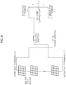
- FIG. 1 is a diagram for illustrating a scheme for applying a reverse voltage to a solar cell array using an additional offset box in an existing photovoltaic system.
- the existing photovoltaic system includes a solar cell array 13, a photovoltaic inverter 10, and a power system 14.
- the photovoltaic inverter 10 includes a DC link capacitor 11 and a power conversion stage 12.
- the DC link capacitor 11 stores a DC voltage output from the photovoltaic array 13. Further, the power conversion stage 12 converts the DC voltage stored in the DC link capacitor 11 into an AC power and supplies the AC power to the power system 14.
- the separate offset box 20 is used to apply a reverse voltage that is opposite in polarity to the voltage applied to the solar cell array 13 during photovoltaic generation.
- the connection between the power conversion stage 12 and the power system 14 and the connection between the solar cell array 13 and the DC link capacitor 11 are cut off, and the high voltage stored in the DC link capacitor 11 is discharged through a rapid discharge circuit.
- the output terminals of the solar cell array 13 are connected to the terminals of the offset box 20 having the opposite polarities, respectively.
- the offset box 20 applies a reverse voltage to the solar cell array 13 to reduce the polarization.
- a power supplied from an external source outside the photovoltaic system is used for reducing the PID, such that residual energy stored in the DC link capacitor cannot be efficiently utilized.
- It another object of the present disclosure to provide a photovoltaic inverter capable of efficiently utilizing the residual energy of photovoltaic generation by using open-circuit voltage output from the solar cell array to reduce the polarization of the solar cell array, instead of discharging the open-circuit voltage.
- a photovoltaic inverter includes: a DC link capacitor configured to store a DC voltage output from the solar cell array; a power conversion stage configured to generate an AC power by using the DC voltage stored in the DC link capacitor to transmit the generated AC power to a power system; and a controller configured to apply the DC voltage stored in the DC link capacitor to the power conversion stage or apply a reverse voltage of the DC voltage stored in the DC link capacitor to the solar cell array depending on whether a driving value of the solar cell array satisfies a predetermined driving condition.
- degradation in the efficiency of photovoltaic generation can be prevented by applying a reverse voltage of a DC voltage stored in a DC link capacitor to a solar cell array.
- the efficiency of photovoltaic generation can be improved by determining whether to apply the DC voltage stored in a DC link capacitor or the reverse voltage thereof based on the magnitude, the driving time, the intensity of polarization of the output voltage of a solar cell array, for example.
- a reverse voltage can be applied to the solar cell array by controlling the switches connecting the solar cell array to the DC link capacitor with no separate module for applying a reverse voltage, thereby saving cost for configuring the photovoltaic system.
- the open-circuit voltage output from the solar cell array is not discharged but is used for reducing the polarization of the solar cell array, such that the residual energy of the photovoltaic power generation can be efficiently utilized.
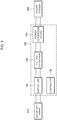
- FIG. 2 is a diagram for illustrating a photovoltaic inverter 100 according to an exemplary embodiment of the present disclosure.
- the photovoltaic inverter 100 according to an exemplary embodiment of the present disclosure includes a DC link capacitor 110, a power conversion stage 120, a controller 130, and a switch unit 140.
- the photovoltaic breaker 100 shown in FIG. 2 is merely an exemplary embodiment of the present disclosure, and the elements are not limited to those shown in FIG. 2 . Some elements may be added, modified or eliminated as desired.
- FIG. 3 is a diagram for illustrating the photovoltaic inverter 100 according to the exemplary embodiment of the present disclosure connected to a solar cell array 310 and a power system 320.
- the photovoltaic inverter 100 and its elements i.e., the DC link capacitor 110, the power conversion stage 120, the controller 130, and the switch unit 140 will be described in detail with reference to FIGS. 2 and 3 .
- the DC link capacitor 110 may store a DC voltage output from the solar cell array 310. More specifically, the DC link capacitor 110 may store the DC voltage output from the solar cell array 310 and transmitted through the switch unit 140. The switch unit 140 may form a transmission path through which the DC voltage output from the solar cell array 310 is transmitted, which will be described later.
- the solar cell array 310 may include one or more solar cell panels connected in series or in parallel that produce electric energy using solar energy.
- the solar cell array 310 may convert the light energy of incident sunlight into DC voltage and output it.
- the DC link capacitor 110 may store the DC voltage output from the solar cell array 310 having a voltage level equal to or greater than a predetermined level in order to supply the voltage to the power conversion stage 120, which will be described later.
- a DC/DC converter which is a step-up circuit, a switching regulator or the like may be disposed between the DC link capacitor 110 and the solar cell array 310.
- the DC link capacitor 110 may store a DC voltage of a predetermined level or more by smoothing the output voltage from the DC/DC converter, the switching regulator, and the like.
- the power conversion stage 120 may generate AC power using the DC voltage stored in the DC link capacitor 110, and may transmit the generated AC power to the power system 320. More specifically, the power conversion stage 120 may convert the DC voltage stored in the DC link capacitor 110 into an alternating current by PWM (Pulse Width Modulation) control.
- PWM Pulse Width Modulation
- the power conversion stage 120 may further include a DC/DC converter for stepping up a DC voltage stored in the DC link capacitor 110, and the like.
- the power conversion stage 120 may convert the DC voltage stepped up by PWM (Pulse Width Modulation) control into alternating current.
- PWM Pulse Width Modulation
- the power system 320 may include a system in which generation and use of electric power is performed.
- the power system 320 may include any system that consumes power from a typical home to a large industrial facility.
- the controller 130 may determine whether the driving value of the solar cell array 310 satisfies a predetermined driving condition.
- the controller 130 may apply the DC voltage stored in the DC link capacitor 110 to the power conversion stage 120 based on the determination result.
- the controller 130 may apply the reverse voltage of the DC voltage stored in the DC link capacitor 110 to the solar cell array 310 based on the determination result.
- the driving value of the solar cell array 310 may include at least one of the magnitude of the DC voltage output from the solar cell array 310, the driving time of the solar cell array 310, the driving time period of the solar cell array 310, and the intensity of polarization of the solar cell array 310.
- the driving time refers to the time at which the solar cell array 310 is currently driven
- the driving time period refers to a continuous time that elapsed since the solar cell array 310 has started being driven until the present time.
- the intensity of polarization [C/m 2 ] is a numerical value representing the amount of the polarized electric charge per unit area or the density of electric dipole moments induced per unit area.
- the driving condition is to drive the solar cell array 310, and may be set according to the driving value of the solar cell array 310. More specifically, if the driving value of the solar cell array 310 is the magnitude of the DC voltage output from the solar cell array 310, the driving condition may be a range of voltages for driving the solar cell array 310.
- the magnitude of the DC voltage output from the solar cell array 310 may be 600 V, and the driving condition, i.e., the range of the driving voltage may be 400 V or higher.
- the magnitude of the DC voltage is greater than 400 V, and thus the driving value of the solar cell array 310 can satisfy the driving condition.
- the driving condition can be satisfied when the driving time of the solar cell array 310 lies within a predetermined driving start time and a predetermined driving end time.
- the driving time of the solar cell array 310 is 5:30 pm
- the driving start time and the driving end time of the solar cell array 310 which are the driving condition, may be 10:00 am and 6:00 pm, respectively.
- the driving value of the solar cell array 310 can satisfy the driving condition of the solar cell array 310.
- the driving condition can be satisfied when the driving time period of the solar cell array 310 lies within a predetermined maximum driving time period.
- the driving time period of the solar cell array 310 is 12 hours, and the maximum driving time of the solar cell array 310, which is the driving condition, may be 10 hours. In this example, the driving time period is greater than 10 hours, the driving value of the solar cell array 310 may not satisfy the driving condition.
- the predetermined driving condition can be satisfied if the intensity of polarization of the solar cell array 310 lies within the range of the intensity of polarization for driving the solar cell array 310.
- the range of the intensity of polarization for driving the solar cell array 310 may be set to be less than a particular intensity of polarization.
- the range of the intensity of polarization may vary depending on the performance of the solar cell and the user's setting.
- the photovoltaic inverter may further include a voltage sensor, a timer, a device for measuring intensity of polarization, etc., for measuring the driving value of the solar cell array 310 described above.
- the controller 130 may apply the DC voltage stored in the DC link capacitor 110 to the power conversion stage 120.
- the controller 130 may apply a reverse voltage of the DC voltage stored in the DC link capacitor 110 to the solar cell array 310.
- the reverse voltage refers to a voltage having the same magnitude as and the opposite polarity to the DC voltage stored in the DC link capacitor 110. For example, if the DC voltage stored in the DC link capacitor 110 is +500 V, the reverse voltage is -500 V.
- the controller 130 controls the switch unit 140 so that the DC voltage stored in the DC link capacitor 110 is applied to the power conversion stage 120 or the reverse voltage of the DC voltage stored in the DC link capacitor 110 is applied to the solar cell array 310.
- the switch unit 140 controlled by the controller 130 will be described in detail with reference to FIGS. 4 to 7 .
- FIG. 4 is a diagram for illustrating the switch unit connected between the solar cell array and the DC link capacitor according to an exemplary embodiment of the present disclosure.
- the switch unit 140 according to the exemplary embodiment of the present disclosure connects the positive terminal and the negative terminal of the solar cell array 310 to the positive terminal and the negative terminal or to the negative terminal and the positive terminal of the DC link capacitor 110, thereby forming a transmission path.
- the switch unit 140 includes a first switch connected between the positive terminal (+) of the solar cell array 310 and the positive terminal (+) of the DC link capacitor 110, a second switch connected between the negative terminal (-) of the solar cell array 310 and the negative terminal (-) of the DC link capacitor 110, a third switch connected between the positive terminal (+) of the solar cell array 310 and the negative terminal (-) of the DC link capacitor 110, and a fourth switch connected between the negative terminal (-) of the solar cell array 310 and the positive terminal (+) of the DC link capacitor 110.
- the first to fourth switches may be turned on or off by a control signal from the controller 130. They may be implemented using switching elements such as a gate turn-off thyristor (GTO), a bipolar junction transistor (BJT), a metal oxide silicon field effect transistor (MOSFET) and an IGBT (insulated gate bipolar mode transistor).
- GTO gate turn-off thyristor
- BJT bipolar junction transistor
- MOSFET metal oxide silicon field effect transistor
- IGBT insulated gate bipolar mode transistor
- FIG. 5 is a diagram illustrating a circuit in which the photovoltaic inverter 100 is connected to the solar cell array 310 according to an exemplary embodiment of the present disclosure.
- the photovoltaic inverter 100 may be configured such that the switch unit 140 including the first to fourth switches, the DC link capacitor 110 and the power conversion stage 120 share the positive terminal and the negative terminal.
- the positive terminal of the photovoltaic inverter 100 may be connected to the positive terminal and the negative terminal of the solar cell array 310 via the first switch and the fourth switch, respectively.
- the negative terminal of the photovoltaic inverter 100 may be connected to the negative terminal and the positive terminal of the solar cell array 310 via the second switch and the third switch, respectively.
- controller 130 may control the first to fourth switches to form a transmission path between the solar cell array 310 and the DC link capacitor 110.
- the power conversion stage 120 may convert a DC voltage stored in the DC link capacitor 110 into alternating current by switching control such as PWM control to generate AC power. To this end, the power conversion stage 120 may include a plurality of switching elements. The power conversion stage 120 may further include a breaker connected to the power system 320 to transmit the generated AC power to the power system 320.
- FIG. 6 is a diagram for illustrating a circuit in a mode to apply a DC voltage stored in the DC link capacitor 110 to the power conversion stage 120.
- the driving value of the solar cell array 310 satisfies a predetermined driving condition, he controller 130 turns on the first switch and the second switch and turns off the third switch and the fourth switch.
- the controller 130 turns on the first and second switches and turns off the third and fourth switches, to form a transmission path.
- the positive terminal and the negative terminal of the solar cell array 310 may be connected to the positive terminal and the negative terminal of the DC link capacitor 110, respectively.
- the DC link capacitor 110 can store the DC voltage V DC output from the solar cell array 310.
- the power conversion stage 120 may convert the DC voltage V DC stored in the DC link capacitor 110 into AC power by the switching control and transmit the AC power to the power system 320 via the circuit breaker.
- FIG. 7 is a diagram illustrating a circuit configured to store an open-circuit voltage (V open ) output from the solar cell array 310 by the DC link capacitor 110 according to an exemplary embodiment of the present disclosure.
- FIG. 8 is a diagram for illustrating a circuit configured to apply a reverse voltage of the DC voltage stored in the DC link capacitor 110 to the solar cell array 310.
- the power conversion stage 120 may interrupt the AC power transmitted to the power system 320. More specifically, if the condition for driving the solar cell array 310 is not satisfied, the power conversion stage 120 may open the circuit breaker to interrupt the connection between the photovoltaic inverter 100 and the power system 320.
- the DC link capacitor 110 may store the open-circuit voltage V open output from the solar cell array 310.
- the internal circuit of the photovoltaic inverter 100 may be an open circuit.
- the output voltage of the solar cell array 310 may be the open-circuit voltage V open
- the DC link capacitor 110 may store the open-circuit voltage V open output from the solar cell array 310.
- the controller 130 may turn off the first switch and the second switch and turn on the third switch and the fourth switch.
- the positive terminal and the negative terminal of the solar cell array 310 may be connected to the negative terminal and the positive terminal of the DC link capacitor 110, respectively.
- the voltage dropped from the positive terminal of the solar cell array 310 to the negative terminal of the solar cell array 310 may be -V DC , which is the reverse voltage of the DC voltage V DC stored in the DC link capacitor 110. Therefore, when the reverse voltage is applied, the positive terminal of the solar cell array 310 may have a potential lower than that of the negative terminal of the solar cell array 310.
- the internal circuit of the photovoltaic inverter 100 may be an open circuit, as described above.
- the DC voltage V DC stored in the DC link may be equal to the open-circuit voltage V open , and the voltage dropped from the positive terminal of the solar cell array 310 to the negative terminal of the photovoltaic cell array 310 may be -V open .
- the open-circuit voltage V open is stored in the DC link capacitor 110. Then, when the controller 130 controls the switch unit 140 to form the transmission path as shown in FIG. 8 , the reverse voltage of the open-circuit voltage V open may be applied to the solar cell array 310.
- a reverse voltage can be applied to the solar cell array by controlling the switches connecting the solar cell array to the DC link capacitor with no separate module for applying the reverse voltage, thereby saving cost for establishing the photovoltaic system.
- the open-circuit voltage output from the solar cell array is not discharged but is used for reducing the polarization of the solar cell array, such that the residual energy of the photovoltaic power generation can be efficiently utilized.
- the controller 130 may control the DC voltage V DC so that the DC voltage V DC output from the solar cell array 310 tracks the maximum power of the solar cell array 310.
- the DC voltage V DC and the current output from the solar cell array 310 have nonlinear characteristics due to factors such as the material of the solar cell array 310. More specifically, the current output from the solar cell array 310 gradually decreases and then decreases sharply in a particular period, as the DC voltage V DC increases.
- the generated power of the solar cell array 310 with respect to the direct-current voltage V DC increases as the DC voltage V DC increases, and decreases sharply when the DC current voltage V DC exceeds a certain voltage.
- the amount of generated power of the solar cell array 310 can be the maximum value.
- the controller 130 may control the magnitude of the voltage V DC output from the solar cell array 310 so that it tracks the maximum power of the solar cell array 310 based on the electric characteristics of the solar cell array 310 (the maximum power point tracking (MPPT)).
- MPPT maximum power point tracking
- the method of controlling the magnitude of the DC voltage V DC output from the solar cell array 310 so that the amount of generated power of the solar cell array 310 tracks the maximum power may be performed according to various embodiments in the related art.
Landscapes
- Engineering & Computer Science (AREA)
- Power Engineering (AREA)
- Photovoltaic Devices (AREA)
- Inverter Devices (AREA)
- Charge And Discharge Circuits For Batteries Or The Like (AREA)
Abstract
Description
- The present disclosure relates to a photovoltaic inverter, and more specifically to a photovoltaic inverter that prevents degradation in the efficiency of photovoltaic generation by applying a reverse voltage of a DC voltage stored in a DC link capacitor to a solar cell array.
- The use of fossil fuels as major energy sources is becoming more and more restricted due to adverse effects such as climate change. Recently, renewable energy is attracting attention as coal and oil are depleted. Accordingly, a renewable energy generation system is becoming important as it is capable of producing environmentally friendly electric power and supplying the produced electric power stably and efficiently.
- Among these, a photovoltaic system prevails since it has advantage that it has less limitations in installing and the size can be freely determined, which meet the requirements in the current situation where energy sources tend to be diversified and decentralized. The photovoltaic system essentially includes a solar cell array and a photovoltaic solar inverter. The photovoltaic inverter serves to convert DC power generated in the solar cell array into AC power.
- Typically, a solar cell array is installed in a metal frame connected to the ground potential. The output terminal of the solar cell array is not connected to the ground potential for stability reasons. Accordingly, a potential difference is created between the metal frame and the solar cell array. If such a potential difference lasts, polarization occurs, i.e., some electrons generated in the solar cell array flow out through the metal frame. Such polarization degrades the efficiency of power generation, which is referred to as potential induced degradation (PID).
- As a known method for improving such PID, it has previously been proposed to apply a reverse voltage to the solar cell array. Hereinafter, an existing photovoltaic system for improving the PID will be described in detail with reference to
FIG. 1 . -
FIG. 1 is a diagram for illustrating a scheme for applying a reverse voltage to a solar cell array using an additional offset box in an existing photovoltaic system. Referring toFIG. 1 , the existing photovoltaic system includes asolar cell array 13, aphotovoltaic inverter 10, and apower system 14. - The
photovoltaic inverter 10 includes aDC link capacitor 11 and apower conversion stage 12. TheDC link capacitor 11 stores a DC voltage output from thephotovoltaic array 13. Further, thepower conversion stage 12 converts the DC voltage stored in theDC link capacitor 11 into an AC power and supplies the AC power to thepower system 14. - According to the existing scheme for reducing the PID, after the photovoltaic generation is stopped, the separate offset box 20 is used to apply a reverse voltage that is opposite in polarity to the voltage applied to the
solar cell array 13 during photovoltaic generation. - More specifically, when the photovoltaic generation is stopped, the connection between the
power conversion stage 12 and thepower system 14 and the connection between thesolar cell array 13 and theDC link capacitor 11 are cut off, and the high voltage stored in theDC link capacitor 11 is discharged through a rapid discharge circuit. - The output terminals of the
solar cell array 13 are connected to the terminals of the offset box 20 having the opposite polarities, respectively. The offset box 20 applies a reverse voltage to thesolar cell array 13 to reduce the polarization. - However, according to the existing scheme, there is a problem that it requires the additional offset box separately installed in addition to the photovoltaic inverter for reducing the PID, incurring unnecessary cost.
- Further, according to the existing scheme, a power supplied from an external source outside the photovoltaic system is used for reducing the PID, such that residual energy stored in the DC link capacitor cannot be efficiently utilized.
- It is an object of the present disclosure to provide a photovoltaic inverter capable of preventing degradation in the efficiency of photovoltaic generation by applying a reverse voltage of a DC voltage stored in a DC link capacitor to a solar cell array.
- It is another object of the present disclosure to provide a photovoltaic inverter capable of improving the efficiency of photovoltaic generation by determining whether to apply the DC voltage stored in a DC link capacitor or the reverse voltage thereof based on the magnitude, the driving time, the intensity of polarization of the output voltage of a solar cell array, for example.
- It is another object of the present disclosure to provide a photovoltaic inverter capable of saving cost for establishing the photovoltaic system by controlling switches connecting a solar cell array to a DC link capacitor to apply a reverse voltage to the solar cell array with no separate module for applying the reverse voltage.
- It another object of the present disclosure to provide a photovoltaic inverter capable of efficiently utilizing the residual energy of photovoltaic generation by using open-circuit voltage output from the solar cell array to reduce the polarization of the solar cell array, instead of discharging the open-circuit voltage.
- Objects of the present disclosure are not limited to the above-described objects and other objects and advantages can be appreciated by those skilled in the art from the following descriptions. Further, it will be easily appreciated that the objects and advantages of the present disclosure can be practiced by means recited in the appended claims and a combination thereof.
- In accordance with one aspect of the present disclosure, a photovoltaic inverter includes: a DC link capacitor configured to store a DC voltage output from the solar cell array; a power conversion stage configured to generate an AC power by using the DC voltage stored in the DC link capacitor to transmit the generated AC power to a power system; and a controller configured to apply the DC voltage stored in the DC link capacitor to the power conversion stage or apply a reverse voltage of the DC voltage stored in the DC link capacitor to the solar cell array depending on whether a driving value of the solar cell array satisfies a predetermined driving condition.
- According to an exemplary embodiment of the present disclosure, degradation in the efficiency of photovoltaic generation can be prevented by applying a reverse voltage of a DC voltage stored in a DC link capacitor to a solar cell array.
- According to another exemplary embodiment of the present disclosure, the efficiency of photovoltaic generation can be improved by determining whether to apply the DC voltage stored in a DC link capacitor or the reverse voltage thereof based on the magnitude, the driving time, the intensity of polarization of the output voltage of a solar cell array, for example.
- According to an exemplary embodiment of the present disclosure, a reverse voltage can be applied to the solar cell array by controlling the switches connecting the solar cell array to the DC link capacitor with no separate module for applying a reverse voltage, thereby saving cost for configuring the photovoltaic system.
- Further, according to an exemplary embodiment of the present disclosure, the open-circuit voltage output from the solar cell array is not discharged but is used for reducing the polarization of the solar cell array, such that the residual energy of the photovoltaic power generation can be efficiently utilized.
-
-
FIG. 1 is a diagram for illustrating a scheme for applying a reverse voltage to a solar cell array using an additional offset box in an existing photovoltaic system; -
FIG. 2 is a diagram for illustrating a photovoltaic inverter according to an exemplary embodiment of the present disclosure; -
FIG. 3 is a diagram for illustrating the photovoltaic inverter according to the exemplary embodiment of the present disclosure connected to a solar cell array and a power system; -
FIG. 4 is a diagram for illustrating the switch unit connected between the solar cell array and the DC link capacitor according to an exemplary embodiment of the present disclosure; -
FIG. 5 is a diagram for illustrating a photovoltaic inverter connected to a solar cell array according to an exemplary embodiment of the present disclosure; -
FIG. 6 is a diagram for illustrating a circuit configured to apply a DC voltage stored in the DC link capacitor to the power conversion stage; -
FIG. 7 is a diagram for illustrating a circuit configured to store an open-circuit voltage output from the solar cell array by the DC link capacitor; and -
FIG. 8 is a diagram for illustrating a circuit configured to apply a reverse voltage of the DC voltage stored in the DC link capacitor to the solar cell array. - The above objects, features and advantages will become apparent from the detailed description with reference to the accompanying drawings. Embodiments are described in sufficient detail to enable those skilled in the art in the art to easily practice the technical idea of the present disclosure. Detailed descriptions of well-known functions or configurations may be omitted in order not to unnecessarily obscure the gist of the present disclosure. Hereinafter, embodiments of the present disclosure will be described in detail with reference to the accompanying drawings. Throughout the drawings, like reference numerals refer to like elements.
-
FIG. 2 is a diagram for illustrating aphotovoltaic inverter 100 according to an exemplary embodiment of the present disclosure. Referring toFIG. 2 , thephotovoltaic inverter 100 according to an exemplary embodiment of the present disclosure includes aDC link capacitor 110, apower conversion stage 120, acontroller 130, and aswitch unit 140. Thephotovoltaic breaker 100 shown inFIG. 2 is merely an exemplary embodiment of the present disclosure, and the elements are not limited to those shown inFIG. 2 . Some elements may be added, modified or eliminated as desired. -
FIG. 3 is a diagram for illustrating thephotovoltaic inverter 100 according to the exemplary embodiment of the present disclosure connected to asolar cell array 310 and apower system 320. Hereinafter, thephotovoltaic inverter 100 and its elements, i.e., theDC link capacitor 110, thepower conversion stage 120, thecontroller 130, and theswitch unit 140 will be described in detail with reference toFIGS. 2 and3 . - Referring to
FIG. 3 , theDC link capacitor 110 according to an exemplary embodiment of the present disclosure may store a DC voltage output from thesolar cell array 310. More specifically, theDC link capacitor 110 may store the DC voltage output from thesolar cell array 310 and transmitted through theswitch unit 140. Theswitch unit 140 may form a transmission path through which the DC voltage output from thesolar cell array 310 is transmitted, which will be described later. - The
solar cell array 310 may include one or more solar cell panels connected in series or in parallel that produce electric energy using solar energy. Thesolar cell array 310 may convert the light energy of incident sunlight into DC voltage and output it. - The
DC link capacitor 110 may store the DC voltage output from thesolar cell array 310 having a voltage level equal to or greater than a predetermined level in order to supply the voltage to thepower conversion stage 120, which will be described later. To this end, a DC/DC converter which is a step-up circuit, a switching regulator or the like may be disposed between theDC link capacitor 110 and thesolar cell array 310. TheDC link capacitor 110 may store a DC voltage of a predetermined level or more by smoothing the output voltage from the DC/DC converter, the switching regulator, and the like. - Referring back to
FIG. 3 , thepower conversion stage 120 may generate AC power using the DC voltage stored in theDC link capacitor 110, and may transmit the generated AC power to thepower system 320. More specifically, thepower conversion stage 120 may convert the DC voltage stored in theDC link capacitor 110 into an alternating current by PWM (Pulse Width Modulation) control. - The
power conversion stage 120 may further include a DC/DC converter for stepping up a DC voltage stored in theDC link capacitor 110, and the like. Thepower conversion stage 120 may convert the DC voltage stepped up by PWM (Pulse Width Modulation) control into alternating current. - The
power system 320 may include a system in which generation and use of electric power is performed. For example, thepower system 320 may include any system that consumes power from a typical home to a large industrial facility. - The
controller 130 according to an exemplary embodiment of the present disclosure may determine whether the driving value of thesolar cell array 310 satisfies a predetermined driving condition. Thecontroller 130 may apply the DC voltage stored in theDC link capacitor 110 to thepower conversion stage 120 based on the determination result. In addition, thecontroller 130 may apply the reverse voltage of the DC voltage stored in theDC link capacitor 110 to thesolar cell array 310 based on the determination result. - The driving value of the
solar cell array 310 may include at least one of the magnitude of the DC voltage output from thesolar cell array 310, the driving time of thesolar cell array 310, the driving time period of thesolar cell array 310, and the intensity of polarization of thesolar cell array 310. - As used herein, the driving time refers to the time at which the
solar cell array 310 is currently driven, and the driving time period refers to a continuous time that elapsed since thesolar cell array 310 has started being driven until the present time. - For example, when the current time is 2:30 pm, for the
solar cell array 310 driven since 10:00 am, the driving time is 2:30 pm, and the driving time period is 4 hours and 30 minutes. The intensity of polarization [C/m2] is a numerical value representing the amount of the polarized electric charge per unit area or the density of electric dipole moments induced per unit area. - The driving condition is to drive the
solar cell array 310, and may be set according to the driving value of thesolar cell array 310. More specifically, if the driving value of thesolar cell array 310 is the magnitude of the DC voltage output from thesolar cell array 310, the driving condition may be a range of voltages for driving thesolar cell array 310. - For example, the magnitude of the DC voltage output from the
solar cell array 310 may be 600 V, and the driving condition, i.e., the range of the driving voltage may be 400 V or higher. In this example, the magnitude of the DC voltage is greater than 400 V, and thus the driving value of thesolar cell array 310 can satisfy the driving condition. - If the driving value of the
solar cell array 310 is the driving time of thesolar cell array 310, the driving condition can be satisfied when the driving time of thesolar cell array 310 lies within a predetermined driving start time and a predetermined driving end time. - For example, the driving time of the
solar cell array 310 is 5:30 pm, and the driving start time and the driving end time of thesolar cell array 310, which are the driving condition, may be 10:00 am and 6:00 pm, respectively. In this example, since the time 5:00 pm is between 10:00 am and 6:00 pm, the driving value of thesolar cell array 310 can satisfy the driving condition of thesolar cell array 310. - When the driving value of the
solar cell array 310 is the driving time period of thesolar cell array 310, the driving condition can be satisfied when the driving time period of thesolar cell array 310 lies within a predetermined maximum driving time period. - For example, the driving time period of the
solar cell array 310 is 12 hours, and the maximum driving time of thesolar cell array 310, which is the driving condition, may be 10 hours. In this example, the driving time period is greater than 10 hours, the driving value of thesolar cell array 310 may not satisfy the driving condition. - If the driving value of the
solar cell array 310 is the intensity of the polarization of thesolar cell array 310, the predetermined driving condition can be satisfied if the intensity of polarization of thesolar cell array 310 lies within the range of the intensity of polarization for driving thesolar cell array 310. - For example, the range of the intensity of polarization for driving the
solar cell array 310 may be set to be less than a particular intensity of polarization. The range of the intensity of polarization may vary depending on the performance of the solar cell and the user's setting. - In addition, according to an exemplary embodiment of the present disclosure, the photovoltaic inverter may further include a voltage sensor, a timer, a device for measuring intensity of polarization, etc., for measuring the driving value of the
solar cell array 310 described above. - As described above, if the driving voltage of the
solar cell array 310 satisfies predetermined driving conditions, thecontroller 130 may apply the DC voltage stored in theDC link capacitor 110 to thepower conversion stage 120. On the other hand, if the driving value of thesolar cell array 310 does not satisfy the predetermined driving conditions, thecontroller 130 may apply a reverse voltage of the DC voltage stored in theDC link capacitor 110 to thesolar cell array 310. - As used herein, the reverse voltage refers to a voltage having the same magnitude as and the opposite polarity to the DC voltage stored in the
DC link capacitor 110. For example, if the DC voltage stored in theDC link capacitor 110 is +500 V, the reverse voltage is -500 V. - In this manner, when the reverse voltage of the DC voltage stored in the
DC link capacitor 110 is applied to thesolar cell array 310, the polarization of the solar cell, which is increased during the solar power generation, can be reduced. As a result, it is possible to prevent degradation in the efficiency of photovoltaic generation. - According to an exemplary embodiment of the present disclosure, it is determined whether to apply the DC voltage stored in the
DC link capacitor 110 or the reverse voltage thereof based on various driving values of thesolar cell array 310, and thus the polarization of the solar cell described above can be reduced, and the efficiency of photovoltaic generation can be also improved. - Referring to
FIG. 3 , thecontroller 130 controls theswitch unit 140 so that the DC voltage stored in theDC link capacitor 110 is applied to thepower conversion stage 120 or the reverse voltage of the DC voltage stored in theDC link capacitor 110 is applied to thesolar cell array 310. Hereinafter, theswitch unit 140 controlled by thecontroller 130 will be described in detail with reference toFIGS. 4 to 7 . -
FIG. 4 is a diagram for illustrating the switch unit connected between the solar cell array and the DC link capacitor according to an exemplary embodiment of the present disclosure. Referring toFIG. 4 , theswitch unit 140 according to the exemplary embodiment of the present disclosure connects the positive terminal and the negative terminal of thesolar cell array 310 to the positive terminal and the negative terminal or to the negative terminal and the positive terminal of theDC link capacitor 110, thereby forming a transmission path. - More specifically, the
switch unit 140 includes a first switch connected between the positive terminal (+) of thesolar cell array 310 and the positive terminal (+) of theDC link capacitor 110, a second switch connected between the negative terminal (-) of thesolar cell array 310 and the negative terminal (-) of theDC link capacitor 110, a third switch connected between the positive terminal (+) of thesolar cell array 310 and the negative terminal (-) of theDC link capacitor 110, and a fourth switch connected between the negative terminal (-) of thesolar cell array 310 and the positive terminal (+) of theDC link capacitor 110. - The first to fourth switches may be turned on or off by a control signal from the
controller 130. They may be implemented using switching elements such as a gate turn-off thyristor (GTO), a bipolar junction transistor (BJT), a metal oxide silicon field effect transistor (MOSFET) and an IGBT (insulated gate bipolar mode transistor). -
FIG. 5 is a diagram illustrating a circuit in which thephotovoltaic inverter 100 is connected to thesolar cell array 310 according to an exemplary embodiment of the present disclosure. Referring toFIG. 5 , thephotovoltaic inverter 100 may be configured such that theswitch unit 140 including the first to fourth switches, theDC link capacitor 110 and thepower conversion stage 120 share the positive terminal and the negative terminal. - The positive terminal of the
photovoltaic inverter 100 may be connected to the positive terminal and the negative terminal of thesolar cell array 310 via the first switch and the fourth switch, respectively. In addition, the negative terminal of thephotovoltaic inverter 100 may be connected to the negative terminal and the positive terminal of thesolar cell array 310 via the second switch and the third switch, respectively. - Although not shown in the drawings, the
controller 130 may control the first to fourth switches to form a transmission path between thesolar cell array 310 and theDC link capacitor 110. - The
power conversion stage 120 may convert a DC voltage stored in theDC link capacitor 110 into alternating current by switching control such as PWM control to generate AC power. To this end, thepower conversion stage 120 may include a plurality of switching elements. Thepower conversion stage 120 may further include a breaker connected to thepower system 320 to transmit the generated AC power to thepower system 320. -
FIG. 6 is a diagram for illustrating a circuit in a mode to apply a DC voltage stored in theDC link capacitor 110 to thepower conversion stage 120. Referring toFIG. 6 , if the driving value of thesolar cell array 310 satisfies a predetermined driving condition, hecontroller 130 turns on the first switch and the second switch and turns off the third switch and the fourth switch. - More specifically, if the condition for driving the
solar cell array 310 is satisfied, thecontroller 130 turns on the first and second switches and turns off the third and fourth switches, to form a transmission path. In other words, if the condition for driving thesolar cell array 310 is satisfied, the positive terminal and the negative terminal of thesolar cell array 310 may be connected to the positive terminal and the negative terminal of theDC link capacitor 110, respectively. - Accordingly, the
DC link capacitor 110 can store the DC voltage VDC output from thesolar cell array 310. Thepower conversion stage 120 may convert the DC voltage VDC stored in theDC link capacitor 110 into AC power by the switching control and transmit the AC power to thepower system 320 via the circuit breaker. -
FIG. 7 is a diagram illustrating a circuit configured to store an open-circuit voltage (Vopen) output from thesolar cell array 310 by theDC link capacitor 110 according to an exemplary embodiment of the present disclosure.FIG. 8 is a diagram for illustrating a circuit configured to apply a reverse voltage of the DC voltage stored in theDC link capacitor 110 to thesolar cell array 310. - Referring to
FIG. 7 , if the driving value of thesolar cell array 310 does not satisfy the predetermined driving condition, thepower conversion stage 120 may interrupt the AC power transmitted to thepower system 320. More specifically, if the condition for driving thesolar cell array 310 is not satisfied, thepower conversion stage 120 may open the circuit breaker to interrupt the connection between thephotovoltaic inverter 100 and thepower system 320. - Referring again to
FIG. 7 , if the driving value of thesolar cell array 310 does not satisfy the predetermined drive condition, theDC link capacitor 110 may store the open-circuit voltage Vopen output from thesolar cell array 310. - More specifically, as described above, when the
power conversion stage 120 turns off the breaker to interrupt the connection between thephotovoltaic inverter 100 and thepower system 320, the internal circuit of thephotovoltaic inverter 100 may be an open circuit. The output voltage of thesolar cell array 310 may be the open-circuit voltage Vopen, and theDC link capacitor 110 may store the open-circuit voltage Vopen output from thesolar cell array 310. - Referring to
FIG. 8 , if the driving value of thesolar cell array 310 does not satisfy the predetermined driving condition, thecontroller 130 may turn off the first switch and the second switch and turn on the third switch and the fourth switch. In other words, if the condition for driving thesolar cell array 310 is satisfied, the positive terminal and the negative terminal of thesolar cell array 310 may be connected to the negative terminal and the positive terminal of theDC link capacitor 110, respectively. - The voltage dropped from the positive terminal of the
solar cell array 310 to the negative terminal of thesolar cell array 310 may be -VDC, which is the reverse voltage of the DC voltage VDC stored in theDC link capacitor 110. Therefore, when the reverse voltage is applied, the positive terminal of thesolar cell array 310 may have a potential lower than that of the negative terminal of thesolar cell array 310. - On the other hand, if the driving value of the
solar cell array 310 does not satisfy the predetermined driving condition, the internal circuit of thephotovoltaic inverter 100 may be an open circuit, as described above. The DC voltage VDC stored in the DC link may be equal to the open-circuit voltage Vopen, and the voltage dropped from the positive terminal of thesolar cell array 310 to the negative terminal of thephotovoltaic cell array 310 may be -Vopen. - As described above, in order to apply the reverse voltage of the open-circuit voltage Vopen to the
solar cell array 310, it may be desirable to open the circuit breaker by thepower conversion stage 120 before thecontroller 130 controls theswitch unit 140. - More specifically, when the
power conversion stage 120 opens the breaker, the open-circuit voltage Vopen is stored in theDC link capacitor 110. Then, when thecontroller 130 controls theswitch unit 140 to form the transmission path as shown inFIG. 8 , the reverse voltage of the open-circuit voltage Vopen may be applied to thesolar cell array 310. - As described above, according to an exemplary embodiment of the present disclosure, a reverse voltage can be applied to the solar cell array by controlling the switches connecting the solar cell array to the DC link capacitor with no separate module for applying the reverse voltage, thereby saving cost for establishing the photovoltaic system.
- Further, according to an exemplary embodiment of the present disclosure, the open-circuit voltage output from the solar cell array is not discharged but is used for reducing the polarization of the solar cell array, such that the residual energy of the photovoltaic power generation can be efficiently utilized.
- According to an exemplary embodiment of the present disclosure, the
controller 130 may control the DC voltage VDC so that the DC voltage VDC output from thesolar cell array 310 tracks the maximum power of thesolar cell array 310. - The DC voltage VDC and the current output from the
solar cell array 310 have nonlinear characteristics due to factors such as the material of thesolar cell array 310. More specifically, the current output from thesolar cell array 310 gradually decreases and then decreases sharply in a particular period, as the DC voltage VDC increases. - Accordingly, the generated power of the
solar cell array 310 with respect to the direct-current voltage VDC increases as the DC voltage VDC increases, and decreases sharply when the DC current voltage VDC exceeds a certain voltage. In other words, when the DC voltage VDC is a certain voltage, the amount of generated power of thesolar cell array 310 can be the maximum value. - According to an exemplary embodiment of the present disclosure, the
controller 130 may control the magnitude of the voltage VDC output from thesolar cell array 310 so that it tracks the maximum power of thesolar cell array 310 based on the electric characteristics of the solar cell array 310 (the maximum power point tracking (MPPT)). - The method of controlling the magnitude of the DC voltage VDC output from the
solar cell array 310 so that the amount of generated power of thesolar cell array 310 tracks the maximum power may be performed according to various embodiments in the related art. - The present disclosure described above may be variously substituted, altered, and modified by those skilled in the art to which the present invention pertains without departing from the scope and sprit of the present disclosure. Therefore, the present disclosure is not limited to the above-mentioned exemplary embodiments and the accompanying drawings.
Claims (7)
- A photovoltaic inverter (100) for applying a reverse voltage to a solar cell array (310), the inverter comprising:a DC link capacitor (110) configured to store a DC voltage output from the solar cell array (310);a power conversion stage (120) configured to generate an AC power by using the DC voltage stored in the DC link capacitor (110) to transmit the generated AC power to a power system (320); anda controller (130) configured to apply the DC voltage stored in the DC link capacitor (110) to the power conversion stage (120) or apply a reverse voltage of the DC voltage stored in the DC link capacitor (110) to the solar cell array (310) depending on whether a driving value of the solar cell array (310) satisfies a predetermined driving condition.
- The photovoltaic inverter (100) of claim 1, wherein the controller (130) is configured to apply the DC voltage stored in the DC link capacitor (110) to the power conversion stage (120) if the driving value of the solar cell array (310) satisfies the predetermined driving condition, and wherein the controller (130) is configured to apply the reverse voltage of the DC voltage stored in the DC link capacitor (110) to the solar cell array (310) if the driving value of the solar cell array (310) does not satisfy the predetermined driving condition.
- The photovoltaic inverter (100) of claim 1 or 2, wherein the power conversion stage (120) is configured to interrupt the AC power transmitted to the power system (320) if the driving value of the solar cell array (310) does not satisfy the predetermined driving condition.
- The photovoltaic inverter (100) of any one of claims 1 to 3, wherein the DC link capacitor (110) is configured to store an open-circuit voltage output from the solar cell array (310) if the driving value of the solar cell array (310) does not satisfy the predetermined driving condition.
- The photovoltaic inverter (100) of any one of claims 1 to 4, wherein the driving value of the solar cell array (310) includes at least one of: a magnitude of the DC voltage output from the solar cell array (310), a driving time of the solar cell array (310), a driving time period of the solar cell array (310), and an intensity of polarization of the solar cell array (310).
- The photovoltaic inverter (100) of any one of claims 1 to 5, further comprising:a switch unit (140),wherein the switch unit (140) comprises a first switch connected between a positive terminal of the solar cell array (310) and a positive terminal of the DC link capacitor (110), a second switch connected between a negative terminal of the solar cell array (310) and a negative terminal of the DC link capacitor (110), a third switch connected between the positive terminal of the solar cell array (310) and the negative terminal of the DC link capacitor (110), and a fourth switch connected between the negative terminal of the solar cell array (310) and the positive terminal of the DC link capacitor (110).
- The photovoltaic inverter (100) of claim 6, wherein the controller (130) turns on the first switch and the second switch and turns off the third switch and the fourth switch if the driving value of the solar cell array (310) satisfies the predetermined driving condition, and wherein the controller (130) turns off the first switch and the second switch and turns on the third switch and the fourth switch if the driving value of the solar cell array (310) does not satisfy the predetermined driving condition.
Applications Claiming Priority (1)
| Application Number | Priority Date | Filing Date | Title |
|---|---|---|---|
| KR1020160109839A KR20180024169A (en) | 2016-08-29 | 2016-08-29 | Photovoltaic inverter |
Publications (2)
| Publication Number | Publication Date |
|---|---|
| EP3291442A1 true EP3291442A1 (en) | 2018-03-07 |
| EP3291442B1 EP3291442B1 (en) | 2019-09-04 |
Family
ID=58714986
Family Applications (1)
| Application Number | Title | Priority Date | Filing Date |
|---|---|---|---|
| EP17171334.0A Active EP3291442B1 (en) | 2016-08-29 | 2017-05-16 | Photovoltaic inverter |
Country Status (6)
| Country | Link |
|---|---|
| US (1) | US10090754B2 (en) |
| EP (1) | EP3291442B1 (en) |
| JP (1) | JP6291111B2 (en) |
| KR (1) | KR20180024169A (en) |
| CN (1) | CN107809212B (en) |
| ES (1) | ES2756707T3 (en) |
Families Citing this family (8)
| Publication number | Priority date | Publication date | Assignee | Title |
|---|---|---|---|---|
| JP6711296B2 (en) * | 2017-02-15 | 2020-06-17 | オムロン株式会社 | Power supply system, DC/DC converter and power conditioner |
| US11258261B2 (en) | 2018-05-10 | 2022-02-22 | Solaredge Technologies Ltd. | Systems and methods to increase the reliability and the service life time of photovoltaic (PV) modules |
| EP3937332A1 (en) | 2018-05-10 | 2022-01-12 | SolarEdge Technologies Ltd. | Systems and methods to increase the reliability and the service life time of photovoltaic (pv) modules |
| CN109742789B (en) * | 2018-12-19 | 2022-05-20 | 广州金升阳科技有限公司 | Photovoltaic power generation system |
| KR102204955B1 (en) | 2019-03-21 | 2021-01-19 | 주식회사 윌링스 | Solar power unit having the function of anti-Potential Induced Degradation |
| CN114285142A (en) * | 2021-12-20 | 2022-04-05 | 珠海格力电器股份有限公司 | Photovoltaic energy storage circuit, control method thereof, photovoltaic air conditioning system and photovoltaic air conditioner |
| US20260033019A1 (en) * | 2022-07-22 | 2026-01-29 | Lasermotive, Inc. | Power receiver electronics |
| KR102582181B1 (en) * | 2023-01-10 | 2023-10-04 | 주식회사 유환 | Solar generating appratus for consistent efficiency with ac shutoff and dc shutoff |
Citations (4)
| Publication number | Priority date | Publication date | Assignee | Title |
|---|---|---|---|---|
| WO2009042795A2 (en) * | 2007-09-26 | 2009-04-02 | Advanced Energy Industries, Inc. | Photovoltaic charge abatement device, system and method |
| US20120280567A1 (en) * | 2011-05-06 | 2012-11-08 | Benyamin Buller | Photovoltaic device |
| CN204068851U (en) * | 2014-09-17 | 2014-12-31 | 英利能源(中国)有限公司 | Inverter |
| CN104333319A (en) * | 2014-11-10 | 2015-02-04 | 许继电气股份有限公司 | Input reverse connection protection circuit for photovoltaic grid-connected inverter |
Family Cites Families (23)
| Publication number | Priority date | Publication date | Assignee | Title |
|---|---|---|---|---|
| JP2002026356A (en) * | 2000-07-04 | 2002-01-25 | Nissin Electric Co Ltd | Snow melting equipment |
| EP1623495B1 (en) * | 2003-05-06 | 2009-10-07 | Enecsys Limited | Power supply circuits |
| JP2005287136A (en) * | 2004-03-29 | 2005-10-13 | Honda Motor Co Ltd | Smoothing capacitor precharge device |
| US7479774B2 (en) * | 2006-04-07 | 2009-01-20 | Yuan Ze University | High-performance solar photovoltaic (PV) energy conversion system |
| US7964837B2 (en) * | 2007-12-31 | 2011-06-21 | Advanced Energy Industries, Inc. | Photovoltaic inverter interface device, system, and method |
| JP5377018B2 (en) * | 2009-03-23 | 2013-12-25 | 株式会社東芝 | Solar power system |
| EP2325984A1 (en) * | 2009-11-24 | 2011-05-25 | SMA Solar Technology AG | Start up of a photovoltiac field with high open circuit voltage |
| US8194375B2 (en) * | 2010-01-19 | 2012-06-05 | General Electric Company | Open circuit voltage protection system and method |
| US8836162B2 (en) * | 2010-02-26 | 2014-09-16 | Ziehl-Abegg Ag | Inverter for photovoltaic systems |
| US8395919B2 (en) * | 2010-07-29 | 2013-03-12 | General Electric Company | Photovoltaic inverter system and method of starting same at high open-circuit voltage |
| DE102010060633B3 (en) * | 2010-11-17 | 2012-04-26 | Sma Solar Technology Ag | Method for connecting a photovoltaic system to a power supply network and photovoltaic system for carrying out the method |
| KR101732984B1 (en) * | 2011-04-12 | 2017-05-08 | 엘지전자 주식회사 | Photovoltaic module and method for controlling the same |
| US9343906B2 (en) * | 2011-06-03 | 2016-05-17 | Schneider Electric Solar Inverters Usa, Inc. | High dynamic DC-voltage controller for photovoltaic inverter |
| CN102544212A (en) | 2011-12-31 | 2012-07-04 | 常州天合光能有限公司 | Power attenuation recovery method of solar component |
| DE102012101340B4 (en) * | 2012-02-20 | 2015-11-19 | Sma Solar Technology Ag | Protection of photovoltaic modules of a photovoltaic generator against overvoltages to earth |
| JP2014099438A (en) * | 2012-11-13 | 2014-05-29 | Nisshinbo Mechatronics Inc | Output drop prevention and recovery device and output drop prevention and recovery method of solar cell module |
| FR3000322B1 (en) * | 2012-12-21 | 2016-05-20 | Schneider Electric Ind Sas | DEVICE FOR PROTECTING AN ELECTRONIC OVERCURRENT OF AT LEAST ONE ELECTRONIC SWITCHING BRANCH, A CONVERSION SYSTEM COMPRISING SUCH A PROTECTIVE DEVICE, AND A CONTROL METHOD THEREFOR |
| KR101442233B1 (en) | 2013-03-08 | 2014-09-24 | 주식회사 루젠 | power control apparatus for solar cell |
| CN203166494U (en) * | 2013-03-26 | 2013-08-28 | 阳光电源(上海)有限公司 | Device for solving potential induced degradation |
| US10615607B2 (en) * | 2013-05-01 | 2020-04-07 | Tigo Energy, Inc. | Systems and methods for quick dissipation of stored energy from input capacitors of power inverters |
| KR20150030078A (en) * | 2013-09-11 | 2015-03-19 | 엘에스산전 주식회사 | Photovoltaic inverter |
| KR20160005613A (en) | 2014-07-07 | 2016-01-15 | 주식회사 케이디파워 | Photovoltaics System |
| CN105720907B (en) * | 2016-01-25 | 2018-02-23 | 南京科远自动化集团股份有限公司 | A kind of method and device for being used in inverter suppress photovoltaic module PID effects |
-
2016
- 2016-08-29 KR KR1020160109839A patent/KR20180024169A/en not_active Ceased
-
2017
- 2017-05-16 EP EP17171334.0A patent/EP3291442B1/en active Active
- 2017-05-16 ES ES17171334T patent/ES2756707T3/en active Active
- 2017-05-18 JP JP2017099152A patent/JP6291111B2/en active Active
- 2017-05-19 US US15/599,640 patent/US10090754B2/en active Active
- 2017-05-27 CN CN201710388084.4A patent/CN107809212B/en active Active
Patent Citations (4)
| Publication number | Priority date | Publication date | Assignee | Title |
|---|---|---|---|---|
| WO2009042795A2 (en) * | 2007-09-26 | 2009-04-02 | Advanced Energy Industries, Inc. | Photovoltaic charge abatement device, system and method |
| US20120280567A1 (en) * | 2011-05-06 | 2012-11-08 | Benyamin Buller | Photovoltaic device |
| CN204068851U (en) * | 2014-09-17 | 2014-12-31 | 英利能源(中国)有限公司 | Inverter |
| CN104333319A (en) * | 2014-11-10 | 2015-02-04 | 许继电气股份有限公司 | Input reverse connection protection circuit for photovoltaic grid-connected inverter |
Non-Patent Citations (2)
| Title |
|---|
| PINGEL S ET AL: "Potential Induced Degradation of solar cells and panels", 35TH IEEE PHOTOVOLTAIC SPECIALISTS CONFERENCE (PVSC), 20-25 JUNE 2010, HONOLULU, HI, USA, IEEE, PISCATAWAY, NJ, USA, 20 June 2010 (2010-06-20), pages 2817 - 2822, XP031786262, ISBN: 978-1-4244-5890-5 * |
| SWANSON R ET AL: "The surface polarization effect in high-efficiency silicon solar cells", PROCEEDINGS OF THE 15TH INTERNATIONAL PHOTOVOLTAIC SCIENCE & ENGINEERING CONFER,, 1 January 2005 (2005-01-01), pages 410 - 411, XP009154074 * |
Also Published As
| Publication number | Publication date |
|---|---|
| US10090754B2 (en) | 2018-10-02 |
| JP6291111B2 (en) | 2018-03-14 |
| KR20180024169A (en) | 2018-03-08 |
| ES2756707T3 (en) | 2020-04-27 |
| JP2018038249A (en) | 2018-03-08 |
| CN107809212A (en) | 2018-03-16 |
| CN107809212B (en) | 2019-08-09 |
| US20180062502A1 (en) | 2018-03-01 |
| EP3291442B1 (en) | 2019-09-04 |
Similar Documents
| Publication | Publication Date | Title |
|---|---|---|
| EP3291442B1 (en) | Photovoltaic inverter | |
| EP1039621B1 (en) | Photovoltaic power generation device | |
| KR101219119B1 (en) | Device, system and method for coupling multiple photovolatic arrays | |
| US8334616B2 (en) | Photovoltaic integrated variable frequency drive | |
| US9806618B2 (en) | Power converting device and power conditioner using the same | |
| US10720776B2 (en) | Optimal power collection control method and apparatus in solar photovoltaic power generation system | |
| US8513913B2 (en) | Photovoltaic system charge controller having buck converter with reversed MOSFETS | |
| CN1697282A (en) | Power supply device and control method used in the power supply device | |
| KR20150048875A (en) | Topology and control strategy for hybrid storage systems | |
| US10396654B2 (en) | Start-up circuit | |
| US20120155141A1 (en) | Power converting apparatus, grid interconnection apparatus and grid interconnection system | |
| KR101035705B1 (en) | Solar battery charge / discharge control device | |
| US10283969B2 (en) | Solar photovoltaic output optimizer circuit | |
| TW201532365A (en) | Topology and control strategy for hybrid storage systems | |
| KR20180111159A (en) | Photovoltaic inverter | |
| JP2004336974A (en) | Power supply | |
| KR101737461B1 (en) | System for obtaining a driving power source to the power generation of the solar cell and method therefor | |
| US20190199216A1 (en) | Power supply apparatus, microbial fuel cell voltage boosting circuit and microbial fuel cell voltage boosting system | |
| CN119813352A (en) | A coordinated control system of photovoltaic-storage DC microgrid converter based on DC bus voltage signal | |
| CN103222181A (en) | Photovoltaic system | |
| KR102030934B1 (en) | Renewable Energy Power Bank | |
| US11791732B2 (en) | Solar photovoltaic output optimizer circuit | |
| EP3079245B1 (en) | Control system and control method for controlling a switching device integrated in an electronic converter and switching cell comprising said system | |
| KR101255470B1 (en) | Battery Energy Storage System | |
| KR102356002B1 (en) | System for solar inverter and operation method thereof |
Legal Events
| Date | Code | Title | Description |
|---|---|---|---|
| PUAI | Public reference made under article 153(3) epc to a published international application that has entered the european phase |
Free format text: ORIGINAL CODE: 0009012 |
|
| STAA | Information on the status of an ep patent application or granted ep patent |
Free format text: STATUS: THE APPLICATION HAS BEEN PUBLISHED |
|
| STAA | Information on the status of an ep patent application or granted ep patent |
Free format text: STATUS: REQUEST FOR EXAMINATION WAS MADE |
|
| AK | Designated contracting states |
Kind code of ref document: A1 Designated state(s): AL AT BE BG CH CY CZ DE DK EE ES FI FR GB GR HR HU IE IS IT LI LT LU LV MC MK MT NL NO PL PT RO RS SE SI SK SM TR |
|
| AX | Request for extension of the european patent |
Extension state: BA ME |
|
| STAA | Information on the status of an ep patent application or granted ep patent |
Free format text: STATUS: EXAMINATION IS IN PROGRESS |
|
| 17P | Request for examination filed |
Effective date: 20180226 |
|
| RBV | Designated contracting states (corrected) |
Designated state(s): AL AT BE BG CH CY CZ DE DK EE ES FI FR GB GR HR HU IE IS IT LI LT LU LV MC MK MT NL NO PL PT RO RS SE SI SK SM TR |
|
| 17Q | First examination report despatched |
Effective date: 20180329 |
|
| GRAP | Despatch of communication of intention to grant a patent |
Free format text: ORIGINAL CODE: EPIDOSNIGR1 |
|
| STAA | Information on the status of an ep patent application or granted ep patent |
Free format text: STATUS: GRANT OF PATENT IS INTENDED |
|
| INTG | Intention to grant announced |
Effective date: 20190430 |
|
| RIN1 | Information on inventor provided before grant (corrected) |
Inventor name: KIM, YOUNG-MIN |
|
| GRAS | Grant fee paid |
Free format text: ORIGINAL CODE: EPIDOSNIGR3 |
|
| GRAA | (expected) grant |
Free format text: ORIGINAL CODE: 0009210 |
|
| STAA | Information on the status of an ep patent application or granted ep patent |
Free format text: STATUS: THE PATENT HAS BEEN GRANTED |
|
| AK | Designated contracting states |
Kind code of ref document: B1 Designated state(s): AL AT BE BG CH CY CZ DE DK EE ES FI FR GB GR HR HU IE IS IT LI LT LU LV MC MK MT NL NO PL PT RO RS SE SI SK SM TR |
|
| REG | Reference to a national code |
Ref country code: GB Ref legal event code: FG4D |
|
| REG | Reference to a national code |
Ref country code: CH Ref legal event code: EP |
|
| REG | Reference to a national code |
Ref country code: AT Ref legal event code: REF Ref document number: 1176786 Country of ref document: AT Kind code of ref document: T Effective date: 20190915 |
|
| REG | Reference to a national code |
Ref country code: DE Ref legal event code: R096 Ref document number: 602017006651 Country of ref document: DE |
|
| REG | Reference to a national code |
Ref country code: IE Ref legal event code: FG4D |
|
| REG | Reference to a national code |
Ref country code: NL Ref legal event code: MP Effective date: 20190904 |
|
| REG | Reference to a national code |
Ref country code: LT Ref legal event code: MG4D |
|
| PG25 | Lapsed in a contracting state [announced via postgrant information from national office to epo] |
Ref country code: FI Free format text: LAPSE BECAUSE OF FAILURE TO SUBMIT A TRANSLATION OF THE DESCRIPTION OR TO PAY THE FEE WITHIN THE PRESCRIBED TIME-LIMIT Effective date: 20190904 Ref country code: SE Free format text: LAPSE BECAUSE OF FAILURE TO SUBMIT A TRANSLATION OF THE DESCRIPTION OR TO PAY THE FEE WITHIN THE PRESCRIBED TIME-LIMIT Effective date: 20190904 Ref country code: BG Free format text: LAPSE BECAUSE OF FAILURE TO SUBMIT A TRANSLATION OF THE DESCRIPTION OR TO PAY THE FEE WITHIN THE PRESCRIBED TIME-LIMIT Effective date: 20191204 Ref country code: HR Free format text: LAPSE BECAUSE OF FAILURE TO SUBMIT A TRANSLATION OF THE DESCRIPTION OR TO PAY THE FEE WITHIN THE PRESCRIBED TIME-LIMIT Effective date: 20190904 Ref country code: NO Free format text: LAPSE BECAUSE OF FAILURE TO SUBMIT A TRANSLATION OF THE DESCRIPTION OR TO PAY THE FEE WITHIN THE PRESCRIBED TIME-LIMIT Effective date: 20191204 Ref country code: LT Free format text: LAPSE BECAUSE OF FAILURE TO SUBMIT A TRANSLATION OF THE DESCRIPTION OR TO PAY THE FEE WITHIN THE PRESCRIBED TIME-LIMIT Effective date: 20190904 |
|
| PG25 | Lapsed in a contracting state [announced via postgrant information from national office to epo] |
Ref country code: LV Free format text: LAPSE BECAUSE OF FAILURE TO SUBMIT A TRANSLATION OF THE DESCRIPTION OR TO PAY THE FEE WITHIN THE PRESCRIBED TIME-LIMIT Effective date: 20190904 Ref country code: GR Free format text: LAPSE BECAUSE OF FAILURE TO SUBMIT A TRANSLATION OF THE DESCRIPTION OR TO PAY THE FEE WITHIN THE PRESCRIBED TIME-LIMIT Effective date: 20191205 Ref country code: AL Free format text: LAPSE BECAUSE OF FAILURE TO SUBMIT A TRANSLATION OF THE DESCRIPTION OR TO PAY THE FEE WITHIN THE PRESCRIBED TIME-LIMIT Effective date: 20190904 Ref country code: RS Free format text: LAPSE BECAUSE OF FAILURE TO SUBMIT A TRANSLATION OF THE DESCRIPTION OR TO PAY THE FEE WITHIN THE PRESCRIBED TIME-LIMIT Effective date: 20190904 |
|
| REG | Reference to a national code |
Ref country code: AT Ref legal event code: MK05 Ref document number: 1176786 Country of ref document: AT Kind code of ref document: T Effective date: 20190904 |
|
| REG | Reference to a national code |
Ref country code: ES Ref legal event code: FG2A Ref document number: 2756707 Country of ref document: ES Kind code of ref document: T3 Effective date: 20200427 |
|
| PG25 | Lapsed in a contracting state [announced via postgrant information from national office to epo] |
Ref country code: RO Free format text: LAPSE BECAUSE OF FAILURE TO SUBMIT A TRANSLATION OF THE DESCRIPTION OR TO PAY THE FEE WITHIN THE PRESCRIBED TIME-LIMIT Effective date: 20190904 Ref country code: EE Free format text: LAPSE BECAUSE OF FAILURE TO SUBMIT A TRANSLATION OF THE DESCRIPTION OR TO PAY THE FEE WITHIN THE PRESCRIBED TIME-LIMIT Effective date: 20190904 Ref country code: NL Free format text: LAPSE BECAUSE OF FAILURE TO SUBMIT A TRANSLATION OF THE DESCRIPTION OR TO PAY THE FEE WITHIN THE PRESCRIBED TIME-LIMIT Effective date: 20190904 Ref country code: PL Free format text: LAPSE BECAUSE OF FAILURE TO SUBMIT A TRANSLATION OF THE DESCRIPTION OR TO PAY THE FEE WITHIN THE PRESCRIBED TIME-LIMIT Effective date: 20190904 Ref country code: PT Free format text: LAPSE BECAUSE OF FAILURE TO SUBMIT A TRANSLATION OF THE DESCRIPTION OR TO PAY THE FEE WITHIN THE PRESCRIBED TIME-LIMIT Effective date: 20200106 Ref country code: AT Free format text: LAPSE BECAUSE OF FAILURE TO SUBMIT A TRANSLATION OF THE DESCRIPTION OR TO PAY THE FEE WITHIN THE PRESCRIBED TIME-LIMIT Effective date: 20190904 |
|
| PG25 | Lapsed in a contracting state [announced via postgrant information from national office to epo] |
Ref country code: SK Free format text: LAPSE BECAUSE OF FAILURE TO SUBMIT A TRANSLATION OF THE DESCRIPTION OR TO PAY THE FEE WITHIN THE PRESCRIBED TIME-LIMIT Effective date: 20190904 Ref country code: CZ Free format text: LAPSE BECAUSE OF FAILURE TO SUBMIT A TRANSLATION OF THE DESCRIPTION OR TO PAY THE FEE WITHIN THE PRESCRIBED TIME-LIMIT Effective date: 20190904 Ref country code: IS Free format text: LAPSE BECAUSE OF FAILURE TO SUBMIT A TRANSLATION OF THE DESCRIPTION OR TO PAY THE FEE WITHIN THE PRESCRIBED TIME-LIMIT Effective date: 20200224 Ref country code: SM Free format text: LAPSE BECAUSE OF FAILURE TO SUBMIT A TRANSLATION OF THE DESCRIPTION OR TO PAY THE FEE WITHIN THE PRESCRIBED TIME-LIMIT Effective date: 20190904 |
|
| REG | Reference to a national code |
Ref country code: DE Ref legal event code: R097 Ref document number: 602017006651 Country of ref document: DE |
|
| PLBE | No opposition filed within time limit |
Free format text: ORIGINAL CODE: 0009261 |
|
| STAA | Information on the status of an ep patent application or granted ep patent |
Free format text: STATUS: NO OPPOSITION FILED WITHIN TIME LIMIT |
|
| PG2D | Information on lapse in contracting state deleted |
Ref country code: IS |
|
| PG25 | Lapsed in a contracting state [announced via postgrant information from national office to epo] |
Ref country code: DK Free format text: LAPSE BECAUSE OF FAILURE TO SUBMIT A TRANSLATION OF THE DESCRIPTION OR TO PAY THE FEE WITHIN THE PRESCRIBED TIME-LIMIT Effective date: 20190904 Ref country code: IS Free format text: LAPSE BECAUSE OF FAILURE TO SUBMIT A TRANSLATION OF THE DESCRIPTION OR TO PAY THE FEE WITHIN THE PRESCRIBED TIME-LIMIT Effective date: 20200105 |
|
| 26N | No opposition filed |
Effective date: 20200605 |
|
| PG25 | Lapsed in a contracting state [announced via postgrant information from national office to epo] |
Ref country code: SI Free format text: LAPSE BECAUSE OF FAILURE TO SUBMIT A TRANSLATION OF THE DESCRIPTION OR TO PAY THE FEE WITHIN THE PRESCRIBED TIME-LIMIT Effective date: 20190904 |
|
| PG25 | Lapsed in a contracting state [announced via postgrant information from national office to epo] |
Ref country code: CH Free format text: LAPSE BECAUSE OF NON-PAYMENT OF DUE FEES Effective date: 20200531 Ref country code: LI Free format text: LAPSE BECAUSE OF NON-PAYMENT OF DUE FEES Effective date: 20200531 Ref country code: MC Free format text: LAPSE BECAUSE OF FAILURE TO SUBMIT A TRANSLATION OF THE DESCRIPTION OR TO PAY THE FEE WITHIN THE PRESCRIBED TIME-LIMIT Effective date: 20190904 |
|
| REG | Reference to a national code |
Ref country code: BE Ref legal event code: MM Effective date: 20200531 |
|
| PG25 | Lapsed in a contracting state [announced via postgrant information from national office to epo] |
Ref country code: LU Free format text: LAPSE BECAUSE OF NON-PAYMENT OF DUE FEES Effective date: 20200516 |
|
| PG25 | Lapsed in a contracting state [announced via postgrant information from national office to epo] |
Ref country code: IE Free format text: LAPSE BECAUSE OF NON-PAYMENT OF DUE FEES Effective date: 20200516 |
|
| PG25 | Lapsed in a contracting state [announced via postgrant information from national office to epo] |
Ref country code: BE Free format text: LAPSE BECAUSE OF NON-PAYMENT OF DUE FEES Effective date: 20200531 |
|
| PG25 | Lapsed in a contracting state [announced via postgrant information from national office to epo] |
Ref country code: TR Free format text: LAPSE BECAUSE OF FAILURE TO SUBMIT A TRANSLATION OF THE DESCRIPTION OR TO PAY THE FEE WITHIN THE PRESCRIBED TIME-LIMIT Effective date: 20190904 Ref country code: MT Free format text: LAPSE BECAUSE OF FAILURE TO SUBMIT A TRANSLATION OF THE DESCRIPTION OR TO PAY THE FEE WITHIN THE PRESCRIBED TIME-LIMIT Effective date: 20190904 Ref country code: CY Free format text: LAPSE BECAUSE OF FAILURE TO SUBMIT A TRANSLATION OF THE DESCRIPTION OR TO PAY THE FEE WITHIN THE PRESCRIBED TIME-LIMIT Effective date: 20190904 |
|
| PG25 | Lapsed in a contracting state [announced via postgrant information from national office to epo] |
Ref country code: MK Free format text: LAPSE BECAUSE OF FAILURE TO SUBMIT A TRANSLATION OF THE DESCRIPTION OR TO PAY THE FEE WITHIN THE PRESCRIBED TIME-LIMIT Effective date: 20190904 |
|
| P01 | Opt-out of the competence of the unified patent court (upc) registered |
Effective date: 20230625 |
|
| PGFP | Annual fee paid to national office [announced via postgrant information from national office to epo] |
Ref country code: DE Payment date: 20250305 Year of fee payment: 9 |
|
| PGFP | Annual fee paid to national office [announced via postgrant information from national office to epo] |
Ref country code: ES Payment date: 20250613 Year of fee payment: 9 |
|
| PGFP | Annual fee paid to national office [announced via postgrant information from national office to epo] |
Ref country code: GB Payment date: 20260309 Year of fee payment: 10 |
|
| PGFP | Annual fee paid to national office [announced via postgrant information from national office to epo] |
Ref country code: IT Payment date: 20260306 Year of fee payment: 10 |
|
| PGFP | Annual fee paid to national office [announced via postgrant information from national office to epo] |
Ref country code: FR Payment date: 20260309 Year of fee payment: 10 |