EP3291295A1 - Pre-bumped redistribution layer structure and semiconductor package incorporating such pre-bumped redistribution layer structure - Google Patents
Pre-bumped redistribution layer structure and semiconductor package incorporating such pre-bumped redistribution layer structure Download PDFInfo
- Publication number
- EP3291295A1 EP3291295A1 EP17179498.5A EP17179498A EP3291295A1 EP 3291295 A1 EP3291295 A1 EP 3291295A1 EP 17179498 A EP17179498 A EP 17179498A EP 3291295 A1 EP3291295 A1 EP 3291295A1
- Authority
- EP
- European Patent Office
- Prior art keywords
- layer
- bump
- bumped
- semiconductor package
- pad
- Prior art date
- Legal status (The legal status is an assumption and is not a legal conclusion. Google has not performed a legal analysis and makes no representation as to the accuracy of the status listed.)
- Withdrawn
Links
Images



Classifications
-
- H—ELECTRICITY
- H10—SEMICONDUCTOR DEVICES; ELECTRIC SOLID-STATE DEVICES NOT OTHERWISE PROVIDED FOR
- H10W—GENERIC PACKAGES, INTERCONNECTIONS, CONNECTORS OR OTHER CONSTRUCTIONAL DETAILS OF DEVICES COVERED BY CLASS H10
- H10W72/00—Interconnections or connectors in packages
- H10W72/20—Bump connectors, e.g. solder bumps or copper pillars; Dummy bumps; Thermal bumps
-
- H—ELECTRICITY
- H10—SEMICONDUCTOR DEVICES; ELECTRIC SOLID-STATE DEVICES NOT OTHERWISE PROVIDED FOR
- H10P—GENERIC PROCESSES OR APPARATUS FOR THE MANUFACTURE OR TREATMENT OF DEVICES COVERED BY CLASS H10
- H10P72/00—Handling or holding of wafers, substrates or devices during manufacture or treatment thereof
- H10P72/70—Handling or holding of wafers, substrates or devices during manufacture or treatment thereof for supporting or gripping
- H10P72/74—Handling or holding of wafers, substrates or devices during manufacture or treatment thereof for supporting or gripping using temporarily an auxiliary support
-
- H—ELECTRICITY
- H10—SEMICONDUCTOR DEVICES; ELECTRIC SOLID-STATE DEVICES NOT OTHERWISE PROVIDED FOR
- H10W—GENERIC PACKAGES, INTERCONNECTIONS, CONNECTORS OR OTHER CONSTRUCTIONAL DETAILS OF DEVICES COVERED BY CLASS H10
- H10W70/00—Package substrates; Interposers; Redistribution layers [RDL]
- H10W70/01—Manufacture or treatment
- H10W70/05—Manufacture or treatment of insulating or insulated package substrates, or of interposers, or of redistribution layers
- H10W70/093—Connecting or disconnecting other interconnections thereto or therefrom, e.g. connecting bond wires or bumps
-
- H—ELECTRICITY
- H10—SEMICONDUCTOR DEVICES; ELECTRIC SOLID-STATE DEVICES NOT OTHERWISE PROVIDED FOR
- H10W—GENERIC PACKAGES, INTERCONNECTIONS, CONNECTORS OR OTHER CONSTRUCTIONAL DETAILS OF DEVICES COVERED BY CLASS H10
- H10W72/00—Interconnections or connectors in packages
-
- H—ELECTRICITY
- H10—SEMICONDUCTOR DEVICES; ELECTRIC SOLID-STATE DEVICES NOT OTHERWISE PROVIDED FOR
- H10W—GENERIC PACKAGES, INTERCONNECTIONS, CONNECTORS OR OTHER CONSTRUCTIONAL DETAILS OF DEVICES COVERED BY CLASS H10
- H10W74/00—Encapsulations, e.g. protective coatings
- H10W74/01—Manufacture or treatment
- H10W74/014—Manufacture or treatment using batch processing
-
- H—ELECTRICITY
- H10—SEMICONDUCTOR DEVICES; ELECTRIC SOLID-STATE DEVICES NOT OTHERWISE PROVIDED FOR
- H10W—GENERIC PACKAGES, INTERCONNECTIONS, CONNECTORS OR OTHER CONSTRUCTIONAL DETAILS OF DEVICES COVERED BY CLASS H10
- H10W90/00—Package configurations
- H10W90/701—Package configurations characterised by the relative positions of pads or connectors relative to package parts
-
- H—ELECTRICITY
- H10—SEMICONDUCTOR DEVICES; ELECTRIC SOLID-STATE DEVICES NOT OTHERWISE PROVIDED FOR
- H10P—GENERIC PROCESSES OR APPARATUS FOR THE MANUFACTURE OR TREATMENT OF DEVICES COVERED BY CLASS H10
- H10P72/00—Handling or holding of wafers, substrates or devices during manufacture or treatment thereof
- H10P72/70—Handling or holding of wafers, substrates or devices during manufacture or treatment thereof for supporting or gripping
- H10P72/74—Handling or holding of wafers, substrates or devices during manufacture or treatment thereof for supporting or gripping using temporarily an auxiliary support
- H10P72/7412—Handling or holding of wafers, substrates or devices during manufacture or treatment thereof for supporting or gripping using temporarily an auxiliary support the auxiliary support including means facilitating the separation of a device or wafer from the auxiliary support
-
- H—ELECTRICITY
- H10—SEMICONDUCTOR DEVICES; ELECTRIC SOLID-STATE DEVICES NOT OTHERWISE PROVIDED FOR
- H10P—GENERIC PROCESSES OR APPARATUS FOR THE MANUFACTURE OR TREATMENT OF DEVICES COVERED BY CLASS H10
- H10P72/00—Handling or holding of wafers, substrates or devices during manufacture or treatment thereof
- H10P72/70—Handling or holding of wafers, substrates or devices during manufacture or treatment thereof for supporting or gripping
- H10P72/74—Handling or holding of wafers, substrates or devices during manufacture or treatment thereof for supporting or gripping using temporarily an auxiliary support
- H10P72/7424—Handling or holding of wafers, substrates or devices during manufacture or treatment thereof for supporting or gripping using temporarily an auxiliary support used as a support during the manufacture of self-supporting substrates
-
- H—ELECTRICITY
- H10—SEMICONDUCTOR DEVICES; ELECTRIC SOLID-STATE DEVICES NOT OTHERWISE PROVIDED FOR
- H10P—GENERIC PROCESSES OR APPARATUS FOR THE MANUFACTURE OR TREATMENT OF DEVICES COVERED BY CLASS H10
- H10P72/00—Handling or holding of wafers, substrates or devices during manufacture or treatment thereof
- H10P72/70—Handling or holding of wafers, substrates or devices during manufacture or treatment thereof for supporting or gripping
- H10P72/74—Handling or holding of wafers, substrates or devices during manufacture or treatment thereof for supporting or gripping using temporarily an auxiliary support
- H10P72/744—Details of chemical or physical process used for separating the auxiliary support from a device or a wafer
-
- H—ELECTRICITY
- H10—SEMICONDUCTOR DEVICES; ELECTRIC SOLID-STATE DEVICES NOT OTHERWISE PROVIDED FOR
- H10W—GENERIC PACKAGES, INTERCONNECTIONS, CONNECTORS OR OTHER CONSTRUCTIONAL DETAILS OF DEVICES COVERED BY CLASS H10
- H10W70/00—Package substrates; Interposers; Redistribution layers [RDL]
- H10W70/60—Insulating or insulated package substrates; Interposers; Redistribution layers
-
- H—ELECTRICITY
- H10—SEMICONDUCTOR DEVICES; ELECTRIC SOLID-STATE DEVICES NOT OTHERWISE PROVIDED FOR
- H10W—GENERIC PACKAGES, INTERCONNECTIONS, CONNECTORS OR OTHER CONSTRUCTIONAL DETAILS OF DEVICES COVERED BY CLASS H10
- H10W72/00—Interconnections or connectors in packages
- H10W72/01—Manufacture or treatment
- H10W72/012—Manufacture or treatment of bump connectors, dummy bumps or thermal bumps
- H10W72/01231—Manufacture or treatment of bump connectors, dummy bumps or thermal bumps using blanket deposition
- H10W72/01233—Manufacture or treatment of bump connectors, dummy bumps or thermal bumps using blanket deposition in liquid form, e.g. spin coating, spray coating or immersion coating
- H10W72/01235—Manufacture or treatment of bump connectors, dummy bumps or thermal bumps using blanket deposition in liquid form, e.g. spin coating, spray coating or immersion coating by plating, e.g. electroless plating or electroplating
-
- H—ELECTRICITY
- H10—SEMICONDUCTOR DEVICES; ELECTRIC SOLID-STATE DEVICES NOT OTHERWISE PROVIDED FOR
- H10W—GENERIC PACKAGES, INTERCONNECTIONS, CONNECTORS OR OTHER CONSTRUCTIONAL DETAILS OF DEVICES COVERED BY CLASS H10
- H10W72/00—Interconnections or connectors in packages
- H10W72/01—Manufacture or treatment
- H10W72/012—Manufacture or treatment of bump connectors, dummy bumps or thermal bumps
- H10W72/01251—Changing the shapes of bumps
- H10W72/01255—Changing the shapes of bumps by using masks
-
- H—ELECTRICITY
- H10—SEMICONDUCTOR DEVICES; ELECTRIC SOLID-STATE DEVICES NOT OTHERWISE PROVIDED FOR
- H10W—GENERIC PACKAGES, INTERCONNECTIONS, CONNECTORS OR OTHER CONSTRUCTIONAL DETAILS OF DEVICES COVERED BY CLASS H10
- H10W72/00—Interconnections or connectors in packages
- H10W72/01—Manufacture or treatment
- H10W72/0198—Manufacture or treatment batch processes
-
- H—ELECTRICITY
- H10—SEMICONDUCTOR DEVICES; ELECTRIC SOLID-STATE DEVICES NOT OTHERWISE PROVIDED FOR
- H10W—GENERIC PACKAGES, INTERCONNECTIONS, CONNECTORS OR OTHER CONSTRUCTIONAL DETAILS OF DEVICES COVERED BY CLASS H10
- H10W72/00—Interconnections or connectors in packages
- H10W72/071—Connecting or disconnecting
- H10W72/072—Connecting or disconnecting of bump connectors
-
- H—ELECTRICITY
- H10—SEMICONDUCTOR DEVICES; ELECTRIC SOLID-STATE DEVICES NOT OTHERWISE PROVIDED FOR
- H10W—GENERIC PACKAGES, INTERCONNECTIONS, CONNECTORS OR OTHER CONSTRUCTIONAL DETAILS OF DEVICES COVERED BY CLASS H10
- H10W72/00—Interconnections or connectors in packages
- H10W72/071—Connecting or disconnecting
- H10W72/072—Connecting or disconnecting of bump connectors
- H10W72/07202—Connecting or disconnecting of bump connectors using auxiliary members
- H10W72/07204—Connecting or disconnecting of bump connectors using auxiliary members using temporary auxiliary members, e.g. sacrificial coatings
- H10W72/07207—Temporary substrates, e.g. removable substrates
-
- H—ELECTRICITY
- H10—SEMICONDUCTOR DEVICES; ELECTRIC SOLID-STATE DEVICES NOT OTHERWISE PROVIDED FOR
- H10W—GENERIC PACKAGES, INTERCONNECTIONS, CONNECTORS OR OTHER CONSTRUCTIONAL DETAILS OF DEVICES COVERED BY CLASS H10
- H10W72/00—Interconnections or connectors in packages
- H10W72/071—Connecting or disconnecting
- H10W72/072—Connecting or disconnecting of bump connectors
- H10W72/07211—Treating the bond pad before connecting, e.g. by applying flux or cleaning
-
- H—ELECTRICITY
- H10—SEMICONDUCTOR DEVICES; ELECTRIC SOLID-STATE DEVICES NOT OTHERWISE PROVIDED FOR
- H10W—GENERIC PACKAGES, INTERCONNECTIONS, CONNECTORS OR OTHER CONSTRUCTIONAL DETAILS OF DEVICES COVERED BY CLASS H10
- H10W72/00—Interconnections or connectors in packages
- H10W72/20—Bump connectors, e.g. solder bumps or copper pillars; Dummy bumps; Thermal bumps
- H10W72/221—Structures or relative sizes
- H10W72/222—Multilayered bumps, e.g. a coating on top and side surfaces of a bump core
-
- H—ELECTRICITY
- H10—SEMICONDUCTOR DEVICES; ELECTRIC SOLID-STATE DEVICES NOT OTHERWISE PROVIDED FOR
- H10W—GENERIC PACKAGES, INTERCONNECTIONS, CONNECTORS OR OTHER CONSTRUCTIONAL DETAILS OF DEVICES COVERED BY CLASS H10
- H10W72/00—Interconnections or connectors in packages
- H10W72/20—Bump connectors, e.g. solder bumps or copper pillars; Dummy bumps; Thermal bumps
- H10W72/241—Dispositions, e.g. layouts
-
- H—ELECTRICITY
- H10—SEMICONDUCTOR DEVICES; ELECTRIC SOLID-STATE DEVICES NOT OTHERWISE PROVIDED FOR
- H10W—GENERIC PACKAGES, INTERCONNECTIONS, CONNECTORS OR OTHER CONSTRUCTIONAL DETAILS OF DEVICES COVERED BY CLASS H10
- H10W72/00—Interconnections or connectors in packages
- H10W72/20—Bump connectors, e.g. solder bumps or copper pillars; Dummy bumps; Thermal bumps
- H10W72/251—Materials
- H10W72/252—Materials comprising solid metals or solid metalloids, e.g. PbSn, Ag or Cu
-
- H—ELECTRICITY
- H10—SEMICONDUCTOR DEVICES; ELECTRIC SOLID-STATE DEVICES NOT OTHERWISE PROVIDED FOR
- H10W—GENERIC PACKAGES, INTERCONNECTIONS, CONNECTORS OR OTHER CONSTRUCTIONAL DETAILS OF DEVICES COVERED BY CLASS H10
- H10W72/00—Interconnections or connectors in packages
- H10W72/50—Bond wires
- H10W72/59—Bond pads specially adapted therefor
-
- H—ELECTRICITY
- H10—SEMICONDUCTOR DEVICES; ELECTRIC SOLID-STATE DEVICES NOT OTHERWISE PROVIDED FOR
- H10W—GENERIC PACKAGES, INTERCONNECTIONS, CONNECTORS OR OTHER CONSTRUCTIONAL DETAILS OF DEVICES COVERED BY CLASS H10
- H10W72/00—Interconnections or connectors in packages
- H10W72/90—Bond pads, in general
- H10W72/921—Structures or relative sizes of bond pads
- H10W72/923—Bond pads having multiple stacked layers
-
- H—ELECTRICITY
- H10—SEMICONDUCTOR DEVICES; ELECTRIC SOLID-STATE DEVICES NOT OTHERWISE PROVIDED FOR
- H10W—GENERIC PACKAGES, INTERCONNECTIONS, CONNECTORS OR OTHER CONSTRUCTIONAL DETAILS OF DEVICES COVERED BY CLASS H10
- H10W72/00—Interconnections or connectors in packages
- H10W72/90—Bond pads, in general
- H10W72/941—Dispositions of bond pads
- H10W72/9415—Dispositions of bond pads relative to the surface, e.g. recessed, protruding
-
- H—ELECTRICITY
- H10—SEMICONDUCTOR DEVICES; ELECTRIC SOLID-STATE DEVICES NOT OTHERWISE PROVIDED FOR
- H10W—GENERIC PACKAGES, INTERCONNECTIONS, CONNECTORS OR OTHER CONSTRUCTIONAL DETAILS OF DEVICES COVERED BY CLASS H10
- H10W72/00—Interconnections or connectors in packages
- H10W72/90—Bond pads, in general
- H10W72/951—Materials of bond pads
- H10W72/952—Materials of bond pads comprising metals or metalloids, e.g. PbSn, Ag or Cu
-
- H—ELECTRICITY
- H10—SEMICONDUCTOR DEVICES; ELECTRIC SOLID-STATE DEVICES NOT OTHERWISE PROVIDED FOR
- H10W—GENERIC PACKAGES, INTERCONNECTIONS, CONNECTORS OR OTHER CONSTRUCTIONAL DETAILS OF DEVICES COVERED BY CLASS H10
- H10W74/00—Encapsulations, e.g. protective coatings
- H10W74/10—Encapsulations, e.g. protective coatings characterised by their shape or disposition
- H10W74/111—Encapsulations, e.g. protective coatings characterised by their shape or disposition the semiconductor body being completely enclosed
- H10W74/114—Encapsulations, e.g. protective coatings characterised by their shape or disposition the semiconductor body being completely enclosed by a substrate and the encapsulations
- H10W74/117—Encapsulations, e.g. protective coatings characterised by their shape or disposition the semiconductor body being completely enclosed by a substrate and the encapsulations the substrate having spherical bumps for external connection
-
- H—ELECTRICITY
- H10—SEMICONDUCTOR DEVICES; ELECTRIC SOLID-STATE DEVICES NOT OTHERWISE PROVIDED FOR
- H10W—GENERIC PACKAGES, INTERCONNECTIONS, CONNECTORS OR OTHER CONSTRUCTIONAL DETAILS OF DEVICES COVERED BY CLASS H10
- H10W74/00—Encapsulations, e.g. protective coatings
- H10W74/10—Encapsulations, e.g. protective coatings characterised by their shape or disposition
- H10W74/15—Encapsulations, e.g. protective coatings characterised by their shape or disposition on active surfaces of flip-chip devices, e.g. underfills
-
- H—ELECTRICITY
- H10—SEMICONDUCTOR DEVICES; ELECTRIC SOLID-STATE DEVICES NOT OTHERWISE PROVIDED FOR
- H10W—GENERIC PACKAGES, INTERCONNECTIONS, CONNECTORS OR OTHER CONSTRUCTIONAL DETAILS OF DEVICES COVERED BY CLASS H10
- H10W90/00—Package configurations
-
- H—ELECTRICITY
- H10—SEMICONDUCTOR DEVICES; ELECTRIC SOLID-STATE DEVICES NOT OTHERWISE PROVIDED FOR
- H10W—GENERIC PACKAGES, INTERCONNECTIONS, CONNECTORS OR OTHER CONSTRUCTIONAL DETAILS OF DEVICES COVERED BY CLASS H10
- H10W90/00—Package configurations
- H10W90/701—Package configurations characterised by the relative positions of pads or connectors relative to package parts
- H10W90/721—Package configurations characterised by the relative positions of pads or connectors relative to package parts of bump connectors
- H10W90/724—Package configurations characterised by the relative positions of pads or connectors relative to package parts of bump connectors between a chip and a stacked insulating package substrate, interposer or RDL
Definitions
- the present invention relates generally to semiconductor packaging and, more particularly, to a semiconductor package incorporating a pre-bumped redistribution layer (RDL) structure.
- RDL redistribution layer
- chip package techniques such as ball grid array (BGA), wire bonding, flip-chip, etc. for mounting a semiconductor die (or chip) on a substrate via the bonding points on both the semiconductor die and the substrate.
- BGA ball grid array
- wire bonding flip-chip
- semiconductor packages are required to be of small in size, multi-pin connection, high speed, and high functionality.
- fan-out wafer level packaging is an embedded type packaging method during wafer level processing and is also a major advanced packaging technology for packaging a large quantity of inputs and outputs (I/O) with high integration flexibility.
- bumped semiconductor dice may be mounted on a package substrate using flip-chip bonding.
- the package substrate may be an interposer that includes metal connections for routing electrical signals between opposite sides.
- the semiconductor dice may be bonded to the substrate through solder bonding. After the die bonding, the semiconductor dice and package substrate are overmolded with a molding compound.
- the "chip-last" packaging process may prevent yield loss of known-good-dies.
- the production cost of the multi-chip package is increased as the number the semiconductor dice in one single package increases because each die in the package needs a separate bumping process, bump mapping, and individual photomask for defining the bump pad openings on each die before die bonding.
- the present invention aims at providing an improved semiconductor package incorporating a pre-bumped redistribution layer (RDL) structure.
- RDL redistribution layer
- the semiconductor package includes a pre-bumped redistribution layer (RDL) structure having opposite first and second surfaces.
- the pre-bumped RDL structure includes at least a bump pad on the first surface and a bump on the bump pad.
- a semiconductor die is mounted on the first surface of the pre-bumped RDL structure.
- the semiconductor die is a flip-chip with its active surface facing toward the pre-bumped RDL structure.
- a plurality of input/output (I/O) pads is disposed on the active surface of the semiconductor die. Each of the plurality of I/O pads is connected to the bump of the pre-bumped RDL structure.
- a molding compound encapsulates the semiconductor die and covers the first surface of the pre-bumped RDL structure.
- a plurality of conductive bumps is mounted on the second surface of the pre-bumped RDL structure.
- a pre-bumped redistribution layer (RDL) structure includes at least a dielectric layer, a first metal layer on the first surface, a second metal layer on the second surface, and a via layer electrically connecting the first metal layer and the second metal layer.
- At least a bump pad is formed in the first metal layer.
- a bump is disposed on the bump pad.
- the bump comprises a copper layer with its lower end directly jointed to a top surface of the bump pad.
- first, second, etc. may be used herein to describe various elements, components, regions, layers and/or sections, these elements, components, regions, layers and/or sections should not be limited by these terms. These terms are only used to distinguish one element, component, region, layer or section from another region, layer or section. Thus, a first element, component, region, layer or section discussed below could be termed a second element, component, region, layer or section without departing from the teachings of the present invention.
- spatially relative terms such as “beneath”, “below”, “lower”, “above”, “upper” and the like, may be used herein for ease of description to describe one element or feature's relationship to another element(s) or feature(s) as illustrated in the figures. It will be understood that the spatially relative terms are intended to encompass different orientations of the device in use or operation in addition to the orientation depicted in the figures. For example, if the device in the figures is turned over, elements described as “below” or “beneath” other elements or features would then be oriented “above” the other elements or features. Thus, the exemplary term “below” can encompass both an orientation of above and below. The device may be otherwise oriented (rotated 90 degrees or at other orientations) and the spatially relative descriptors used herein interpreted accordingly.
- horizontal as used herein is defined as a plane parallel to a major plane or surface of the substrate, regardless of its orientation.
- vertical refers to a direction perpendicular to the horizontal as just defined. Terms, such as “on”, “above”, “below”, “bottom”, “top”, “side” (as in “sidewall”), "higher”, “lower”, “over”, and “under”, are defined with respect to the horizontal plane.
- the present invention pertains to a pre-bumped redistribution layer (RDL) structure and a semiconductor package incorporating such pre-bumped RDL structure.
- the semiconductor package may be a single-die package or a multi-die package.
- FIG. 1 to FIG. 4 illustrate an exemplary method for fabricating a semiconductor package incorporating a pre-bumped redistribution layer (RDL) structure according to one embodiment of the invention.
- RDL redistribution layer
- a carrier substrate 100 is provided.
- the carrier substrate 100 may comprise glass, silicon, ceramic, or metal, but is not limited thereto.
- a release layer 102 may be formed on a top surface of the carrier substrate 100.
- a redistribution layer (RDL) structure 120 is then formed on the release layer 102.
- the RDL structure 120 may comprise at least a dielectric layer 125, a metal layer 121, a metal layer 122, and a via layer 123 electrically connecting the metal layer 121 and the metal layer 122.
- the metal layer 121 may comprise conductive bump pads 121a and metal traces not explicitly shown in this figure, and the metal layer 122 may comprise bump pads 122a and metal traces 122b. It is understood that the layers and patterns in the RDL structure 120 as depicted in the figures are for illustration purposes only. The number of the metal layers in the RDL structure 120 may depend upon the design requirements.
- the metal layers 121 and 122, and the via layer 123 may comprise aluminum, copper, tungsten, titanium, titanium nitride, or the like.
- the dielectric layer 125 may comprise any suitable insulating materials including, but not limited to, photo image dielectric (PID) materials, prepreg, resin materials such as Ajinomoto Build-up Film (ABF) or the like.
- the metal patterns in the dielectric layer 125 may be formed by build-up processes and plating processes, but is not limited thereto.
- the dielectric layer 125 may comprise inorganic materials such as silicon oxide, silicon nitride or the like, and the metal patterns in the dielectric layer 125 may be formed by photolithographic processes and etching processes.
- the metal traces or metal patterns formed in the dielectric layer 125 may have a line width ranging between 1 ⁇ 10 micrometers and a space (between two adjacent lines) ranging between 1 ⁇ 10 micrometers, but is not limited thereto.
- a mask 130 such as a dielectric layer or a solder mask may be formed on the dielectric layer 125 and the metal layer 122.
- the mask 130 may comprise a plurality of openings 131 that expose the bump pads 122a of the metal layer 122, respectively.
- bumps 140 are formed on the bump pads 122a, respectively, thereby forming a pre-bumped RDL structure 120a.
- the bumps 140 may comprise metals such tin, copper, silver, or gold, but is not limited thereto.
- the bumps 140 are copper pillars.
- a seed layer such as a copper seed layer may be formed on the bump pads 122a, and then a resist layer (not shown) for defining the pattern and location of the bumps 140 may be formed on the seed layer. Thereafter, a plating process may be performed to form the bumps 140 such as copper pillar bumps. The resist layer is then removed. The seed layer not covered by the bumps 140 is also removed.
- the bump 140 may further comprise an intermediate metal layer 142.
- the intermediate metal layer 142 may comprise nickel or a nickel-containing layer, but is not limited thereto.
- the bump 140 may further comprise a solder layer 144 provided directly on the intermediate metal layer 142.
- the solder layer 144 may be a lead-free pre-solder layer formed of, for example, SnAg, or a solder material, including alloys of tin, lead, silver, copper, nickel, bismuth, or combinations thereof.
- a semiconductor die 200 is mounted within each chip mounting area on the pre-bumped RDL structure 120a.
- the semiconductor die 200 is a flip-chip with its active surface 200a facing down toward the pre-bumped RDL structure 120a.
- a plurality of input/output (I/O) pads 201 may be disposed on the active surface 200a of the semiconductor die 200.
- the semiconductor package may be a multi-die package.
- two or more than two semiconductor dice 200 are mounted within chip mounting areas, respectively, on the pre-bumped RDL structure 120a, and each of the semiconductor dice 200 is a flip-chip with its active surface 200a facing down toward the pre-bumped RDL structure 120a.
- a plurality of input/output (I/O) pads 201 may be disposed on the active surface 200a of each of the semiconductor dice 200.
- FIGS. 5-7 are schematic, enlarged partial views showing various bonding structures between the semiconductor die 200 and the pre-bumped RDL structure 120a according to various embodiments of the invention.
- each of the I/O pads 201 of the semiconductor die 200 has a top surface, which may be an aluminum (or copper) surface of the I/O pad itself, exposed from a passivation layer 203.
- no additional connecting element such as a metal bump or a metal pillar is disposed on the top surface of each of the I/O pads 201 before die bonding.
- the top surface of each of the I/O pads 201 is directly coupled to a corresponding bump 140 through, for example, the solder layer 144.
- a surface finish layer such as organic solderability preservatives (OSP) may be provided on exposed top surface of each of the I/O pads 201.
- OSP organic solderability preservatives
- the bump 140 comprises a copper layer 141 with its lower end (or bottom surface) directly jointed to a top surface of the bump pad 122a. That is, no solder or pre-solder is disposed between the copper layer 141 of the bump 140 and the bump pad 122a.
- FIG. 5 shows that the bonding structure has the solder layer 144 that is disposed only between the copper layer 141 and the I/O pad 201. The solder layer 144 is situated closer to the semiconductor die 200 than the copper layer 141 of the bump 140. Further, a cross-sectional area of the solder layer 144 is equal to that of the copper layer 141.
- each of the I/O pads 201 of the semiconductor die 200 has a top surface, which may be an aluminum (or copper) surface of the I/O pad itself.
- an under bump metal (UBM) layer 202 is formed on the top surface of each of the I/O pads 201.
- no metal bump e.g. copper bump
- metal pillar e.g. copper pillar
- Each of the I/O pads 201 of the semiconductor die 200 is coupled to a corresponding bump 140 through, for example, the UBM layer 202 pre-fabricated on the I/O pad 201 and the solder layer 144 of the bump 140.
- the solder layer 144 is situated closer to the semiconductor die 200 than the copper layer 141 of the bump 140. Further, a cross-sectional area of the solder layer 144 is equal to that of the copper layer 141.
- each of the I/O pads 201 of the semiconductor die 200 has a top surface, which may be an aluminum (or copper) surface of the I/O pad itself.
- an under bump metal (UBM) layer 202 is formed on the top surface of each of the I/O pads 201.
- a pre-solder layer 204 is formed on the UBM layer 202.
- Each of the I/O pads 201 of the semiconductor die 200 is coupled to a corresponding bump 140 through, for example, the UBM layer 202 and the pre-solder layer 204 pre-fabricated on the I/O pad 201.
- the intermediate metal layer 142 and the solder layer 144 may be omitted.
- the solder layer 144 is situated closer to the semiconductor die 200 than the copper layer 141 of the bump 140. Further, a cross-sectional area of the solder layer 144 is greater to that of the copper layer 141.
- a molding compound 300 is applied.
- the molding compound 300 at least covers the semiconductor dice 200 and the top surface of the pre-bumped RDL structure 120a.
- the molding compound 300 may be subjected to a curing process.
- the molding compound 300 may comprise a mixture of epoxy and silica fillers, but not limited thereto.
- an underfill 310 may be applied between each of the semiconductor dice 200 and the pre-bumped RDL structure 120a.
- the underfill 310 may be a silica filled epoxy, but is not limited thereto.
- the underfill 310 fills the gap (or standoff) between each of the semiconductor dice 200 and the pre-bumped RDL structure 120a.
- the carrier substrate 100 and the release layer 102 are removed to thereby expose a lower surface of the pre-bumped RDL structure 120a.
- the de-bonding of the carrier substrate 100 may be performed by using heating, laser, UV/IR irradiation, or mechanical peeling, but not limited thereto.
- a lower surface of each of the conductive bump pads 121a of the metal layer 121 is revealed.
- no metal finish is formed on the exposed lower surface of each of the conductive bump pads 121a of the metal layer 121.
- the thickness of the metal layer 121 may range between 1 and 20 micrometers.
- a metal finish such as Ni, Au, and/or other elemental metals may be formed on the exposed lower surface of each of the conductive bump pads 121 a of the metal layer 121.
- conductive bumps 410 are disposed on respective conductive bump pads 121a of the metal layer 121 to complete a wafer level package.
- the wafer level package is then subjected to a wafer dicing process and singulated into semiconductor packages 1.
- the bumps 140 are pre-fabricated on the RDL structure 120 (pre-bumped RDL structure 120a). Therefore, masks for individual bumping on each die may be spared and the production cost is reduced. In addition, bumps on the I/O pads on each of the die can be omitted, thereby saving the process time of the semiconductor packages.
Landscapes
- Internal Circuitry In Semiconductor Integrated Circuit Devices (AREA)
Abstract
Description
- The present invention relates generally to semiconductor packaging and, more particularly, to a semiconductor package incorporating a pre-bumped redistribution layer (RDL) structure.
- As known in the art, there are a variety of chip package techniques such as ball grid array (BGA), wire bonding, flip-chip, etc. for mounting a semiconductor die (or chip) on a substrate via the bonding points on both the semiconductor die and the substrate. To ensure miniaturization and multi-functionality of electronic products or communication devices, semiconductor packages are required to be of small in size, multi-pin connection, high speed, and high functionality.
- For example, fan-out wafer level packaging (FOWLP) is an embedded type packaging method during wafer level processing and is also a major advanced packaging technology for packaging a large quantity of inputs and outputs (I/O) with high integration flexibility.
- In a "chip-last" packaging process, bumped semiconductor dice may be mounted on a package substrate using flip-chip bonding. The package substrate may be an interposer that includes metal connections for routing electrical signals between opposite sides. The semiconductor dice may be bonded to the substrate through solder bonding. After the die bonding, the semiconductor dice and package substrate are overmolded with a molding compound.
- The "chip-last" packaging process may prevent yield loss of known-good-dies. However, the production cost of the multi-chip package is increased as the number the semiconductor dice in one single package increases because each die in the package needs a separate bumping process, bump mapping, and individual photomask for defining the bump pad openings on each die before die bonding.
- This in mind, the present invention aims at providing an improved semiconductor package incorporating a pre-bumped redistribution layer (RDL) structure.
- This is achieved by a semiconductor package according to the pre-characterizing clause of
claim 1. The dependent claims pertain to corresponding further developments and improvements. - As will be seen more clearly from the detailed description following below, the semiconductor package includes a pre-bumped redistribution layer (RDL) structure having opposite first and second surfaces. The pre-bumped RDL structure includes at least a bump pad on the first surface and a bump on the bump pad. A semiconductor die is mounted on the first surface of the pre-bumped RDL structure. The semiconductor die is a flip-chip with its active surface facing toward the pre-bumped RDL structure. A plurality of input/output (I/O) pads is disposed on the active surface of the semiconductor die. Each of the plurality of I/O pads is connected to the bump of the pre-bumped RDL structure. A molding compound encapsulates the semiconductor die and covers the first surface of the pre-bumped RDL structure. A plurality of conductive bumps is mounted on the second surface of the pre-bumped RDL structure.
- According to another aspect of the invention, a pre-bumped redistribution layer (RDL) structure is disclosed. The pre-bumped RDL structure includes at least a dielectric layer, a first metal layer on the first surface, a second metal layer on the second surface, and a via layer electrically connecting the first metal layer and the second metal layer. At least a bump pad is formed in the first metal layer. A bump is disposed on the bump pad. The bump comprises a copper layer with its lower end directly jointed to a top surface of the bump pad.
- These and other objectives of the present invention will no doubt become obvious to those of ordinary skill in the art after reading the following detailed description of the preferred embodiment that is illustrated in the various figures and drawings.
- The accompanying drawings are included to provide a further understanding of the embodiments, and are incorporated in and constitute a part of this specification. The drawings illustrate some of the embodiments and, together with the description, serve to explain their principles. In the drawings:
-
FIG. 1 to FIG. 4 illustrate an exemplary method for fabricating a semiconductor package incorporating a pre-bumped redistribution layer (RDL) structure according to one embodiment of the invention; and -
FIGS. 5-7 are schematic, enlarged partial views showing various bonding structures between the semiconductor die and the pre-bumped RDL structure according to embodiments of the invention. - In the following detailed description of the disclosure, reference is made to the accompanying drawings, which form a part hereof, and in which is shown, by way of illustration, specific embodiments in which the invention may be practiced. These embodiments are described in sufficient detail to enable those skilled in the art to practice the invention. Other embodiments may be utilized and structural changes may be made without departing from the scope of the present disclosure.
- The following detailed description is, therefore, not to be taken in a limiting sense, and the scope of the present invention is defined only by the appended claims, along with the full scope of equivalents to which such claims are entitled.
- One or more implementations of the present invention will now be described with reference to the attached drawings, wherein like reference numerals are used to refer to like elements throughout, and wherein the illustrated structures are not necessarily drawn to scale.
- It will be understood that when an element or layer is referred to as being "on", "connected to" or "coupled to" another element or layer, it can be directly on, connected or coupled to the other element or layer or intervening elements or layers may be present. In contrast, when an element is referred to as being "directly on," "directly connected to" or "directly coupled to" another element or layer, there are no intervening elements or layers present. Like numbers refer to like elements throughout.
- It will be understood that, although the terms first, second, etc. may be used herein to describe various elements, components, regions, layers and/or sections, these elements, components, regions, layers and/or sections should not be limited by these terms. These terms are only used to distinguish one element, component, region, layer or section from another region, layer or section. Thus, a first element, component, region, layer or section discussed below could be termed a second element, component, region, layer or section without departing from the teachings of the present invention.
- Spatially relative terms, such as "beneath", "below", "lower", "above", "upper" and the like, may be used herein for ease of description to describe one element or feature's relationship to another element(s) or feature(s) as illustrated in the figures. It will be understood that the spatially relative terms are intended to encompass different orientations of the device in use or operation in addition to the orientation depicted in the figures. For example, if the device in the figures is turned over, elements described as "below" or "beneath" other elements or features would then be oriented "above" the other elements or features. Thus, the exemplary term "below" can encompass both an orientation of above and below. The device may be otherwise oriented (rotated 90 degrees or at other orientations) and the spatially relative descriptors used herein interpreted accordingly.
- The term "horizontal" as used herein is defined as a plane parallel to a major plane or surface of the substrate, regardless of its orientation. The term "vertical" refers to a direction perpendicular to the horizontal as just defined. Terms, such as "on", "above", "below", "bottom", "top", "side" (as in "sidewall"), "higher", "lower", "over", and "under", are defined with respect to the horizontal plane.
- The present invention pertains to a pre-bumped redistribution layer (RDL) structure and a semiconductor package incorporating such pre-bumped RDL structure. The semiconductor package may be a single-die package or a multi-die package.
-
FIG. 1 to FIG. 4 illustrate an exemplary method for fabricating a semiconductor package incorporating a pre-bumped redistribution layer (RDL) structure according to one embodiment of the invention. - As shown in
FIG. 1 , acarrier substrate 100 is provided. According to one embodiment, thecarrier substrate 100 may comprise glass, silicon, ceramic, or metal, but is not limited thereto. According to one embodiment, arelease layer 102 may be formed on a top surface of thecarrier substrate 100. - A redistribution layer (RDL)
structure 120 is then formed on therelease layer 102. TheRDL structure 120 may comprise at least adielectric layer 125, ametal layer 121, ametal layer 122, and avia layer 123 electrically connecting themetal layer 121 and themetal layer 122. - According to one embodiment, for example, the
metal layer 121 may compriseconductive bump pads 121a and metal traces not explicitly shown in this figure, and themetal layer 122 may comprisebump pads 122a andmetal traces 122b. It is understood that the layers and patterns in theRDL structure 120 as depicted in the figures are for illustration purposes only. The number of the metal layers in theRDL structure 120 may depend upon the design requirements. - According to one embodiment, the metal layers 121 and 122, and the via
layer 123 may comprise aluminum, copper, tungsten, titanium, titanium nitride, or the like. Thedielectric layer 125 may comprise any suitable insulating materials including, but not limited to, photo image dielectric (PID) materials, prepreg, resin materials such as Ajinomoto Build-up Film (ABF) or the like. - According to one embodiment, the metal patterns in the
dielectric layer 125 may be formed by build-up processes and plating processes, but is not limited thereto. In another embodiment, thedielectric layer 125 may comprise inorganic materials such as silicon oxide, silicon nitride or the like, and the metal patterns in thedielectric layer 125 may be formed by photolithographic processes and etching processes. - According to one embodiment, the metal traces or metal patterns formed in the
dielectric layer 125 may have a line width ranging between 1∼10 micrometers and a space (between two adjacent lines) ranging between 1∼10 micrometers, but is not limited thereto. - According to one embodiment, optionally, a
mask 130 such as a dielectric layer or a solder mask may be formed on thedielectric layer 125 and themetal layer 122. Themask 130 may comprise a plurality ofopenings 131 that expose thebump pads 122a of themetal layer 122, respectively. - As shown in
FIG. 2 , subsequently, bumps 140 are formed on thebump pads 122a, respectively, thereby forming apre-bumped RDL structure 120a. According to one embodiment, thebumps 140 may comprise metals such tin, copper, silver, or gold, but is not limited thereto. According to one embodiment, thebumps 140 are copper pillars. - To form the
bumps 140 on thebump pads 122a, for example, a seed layer (not shown) such as a copper seed layer may be formed on thebump pads 122a, and then a resist layer (not shown) for defining the pattern and location of thebumps 140 may be formed on the seed layer. Thereafter, a plating process may be performed to form thebumps 140 such as copper pillar bumps. The resist layer is then removed. The seed layer not covered by thebumps 140 is also removed. - Optionally, the
bump 140 may further comprise anintermediate metal layer 142. For example, theintermediate metal layer 142 may comprise nickel or a nickel-containing layer, but is not limited thereto. Optionally, thebump 140 may further comprise asolder layer 144 provided directly on theintermediate metal layer 142. Thesolder layer 144 may be a lead-free pre-solder layer formed of, for example, SnAg, or a solder material, including alloys of tin, lead, silver, copper, nickel, bismuth, or combinations thereof. - As shown in
FIG. 3 , asemiconductor die 200 is mounted within each chip mounting area on thepre-bumped RDL structure 120a. According to one embodiment, the semiconductor die 200 is a flip-chip with itsactive surface 200a facing down toward thepre-bumped RDL structure 120a. A plurality of input/output (I/O)pads 201 may be disposed on theactive surface 200a of the semiconductor die 200. - According to another embodiment, the semiconductor package may be a multi-die package. For example, two or more than two
semiconductor dice 200 are mounted within chip mounting areas, respectively, on thepre-bumped RDL structure 120a, and each of thesemiconductor dice 200 is a flip-chip with itsactive surface 200a facing down toward thepre-bumped RDL structure 120a. A plurality of input/output (I/O)pads 201 may be disposed on theactive surface 200a of each of thesemiconductor dice 200. - Please also refer briefly to
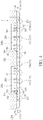
FIGS. 5-7. FIGS. 5-7 are schematic, enlarged partial views showing various bonding structures between the semiconductor die 200 and thepre-bumped RDL structure 120a according to various embodiments of the invention. - As shown in
FIG. 5 , according to one embodiment, each of the I/O pads 201 of the semiconductor die 200 has a top surface, which may be an aluminum (or copper) surface of the I/O pad itself, exposed from apassivation layer 203. In other words, no additional connecting element such as a metal bump or a metal pillar is disposed on the top surface of each of the I/O pads 201 before die bonding. The top surface of each of the I/O pads 201 is directly coupled to acorresponding bump 140 through, for example, thesolder layer 144. Optionally, according to another embodiment, a surface finish layer (not explicitly shown) such as organic solderability preservatives (OSP) may be provided on exposed top surface of each of the I/O pads 201. - In
FIG. 5 , according to one embodiment, thebump 140 comprises acopper layer 141 with its lower end (or bottom surface) directly jointed to a top surface of thebump pad 122a. That is, no solder or pre-solder is disposed between thecopper layer 141 of thebump 140 and thebump pad 122a.FIG. 5 shows that the bonding structure has thesolder layer 144 that is disposed only between thecopper layer 141 and the I/O pad 201. Thesolder layer 144 is situated closer to the semiconductor die 200 than thecopper layer 141 of thebump 140. Further, a cross-sectional area of thesolder layer 144 is equal to that of thecopper layer 141. - As shown in
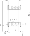
FIG. 6 , each of the I/O pads 201 of the semiconductor die 200 has a top surface, which may be an aluminum (or copper) surface of the I/O pad itself. According to this embodiment, an under bump metal (UBM)layer 202 is formed on the top surface of each of the I/O pads 201. However, no metal bump (e.g. copper bump) or metal pillar (e.g. copper pillar) is disposed on theUBM layer 202. Each of the I/O pads 201 of the semiconductor die 200 is coupled to acorresponding bump 140 through, for example, theUBM layer 202 pre-fabricated on the I/O pad 201 and thesolder layer 144 of thebump 140. Thesolder layer 144 is situated closer to the semiconductor die 200 than thecopper layer 141 of thebump 140. Further, a cross-sectional area of thesolder layer 144 is equal to that of thecopper layer 141. - As shown in
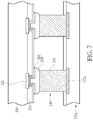
FIG. 7 , each of the I/O pads 201 of the semiconductor die 200 has a top surface, which may be an aluminum (or copper) surface of the I/O pad itself. According to this embodiment, an under bump metal (UBM)layer 202 is formed on the top surface of each of the I/O pads 201. Apre-solder layer 204 is formed on theUBM layer 202. Each of the I/O pads 201 of the semiconductor die 200 is coupled to acorresponding bump 140 through, for example, theUBM layer 202 and thepre-solder layer 204 pre-fabricated on the I/O pad 201. In a case as depicted inFIG. 7 , it is understood that theintermediate metal layer 142 and thesolder layer 144 may be omitted. According to this embodiment, thesolder layer 144 is situated closer to the semiconductor die 200 than thecopper layer 141 of thebump 140. Further, a cross-sectional area of thesolder layer 144 is greater to that of thecopper layer 141. - As shown in
FIG. 4 , after mounting thesemiconductor dice 200 on thepre-bumped RDL structure 120a, amolding compound 300 is applied. Themolding compound 300 at least covers thesemiconductor dice 200 and the top surface of thepre-bumped RDL structure 120a. According to one embodiment, themolding compound 300 may be subjected to a curing process. Themolding compound 300 may comprise a mixture of epoxy and silica fillers, but not limited thereto. - According to another embodiment, prior to the formation of the
molding compound 300, anunderfill 310 may be applied between each of thesemiconductor dice 200 and thepre-bumped RDL structure 120a. Theunderfill 310 may be a silica filled epoxy, but is not limited thereto. Theunderfill 310 fills the gap (or standoff) between each of thesemiconductor dice 200 and thepre-bumped RDL structure 120a. - Subsequently, the
carrier substrate 100 and therelease layer 102 are removed to thereby expose a lower surface of thepre-bumped RDL structure 120a. The de-bonding of thecarrier substrate 100 may be performed by using heating, laser, UV/IR irradiation, or mechanical peeling, but not limited thereto. After thecarrier substrate 100 is removed, a lower surface of each of theconductive bump pads 121a of themetal layer 121 is revealed. - According to one embodiment, no metal finish is formed on the exposed lower surface of each of the
conductive bump pads 121a of themetal layer 121. The thickness of themetal layer 121 may range between 1 and 20 micrometers. According to another embodiment, a metal finish such as Ni, Au, and/or other elemental metals may be formed on the exposed lower surface of each of theconductive bump pads 121 a of themetal layer 121. - Subsequently,
conductive bumps 410 are disposed on respectiveconductive bump pads 121a of themetal layer 121 to complete a wafer level package. The wafer level package is then subjected to a wafer dicing process and singulated into semiconductor packages 1. - It is advantageous to use the invention because the
bumps 140 are pre-fabricated on the RDL structure 120 (pre-bumped RDL structure 120a). Therefore, masks for individual bumping on each die may be spared and the production cost is reduced. In addition, bumps on the I/O pads on each of the die can be omitted, thereby saving the process time of the semiconductor packages.
Claims (23)
- A semiconductor package (1), comprising:a pre-bumped redistribution layer (RDL) structure (120a) having opposite first and second surfaces, wherein the pre-bumped RDL structure (120a) comprises at least a bump pad (122a) on the first surface and a bump (140) on the bump pad (122a);a semiconductor die (200) mounted on the first surface of the pre-bumped RDL structure (120a), wherein the semiconductor die (200) is a flip-chip with its active surface (200a) facing toward the pre-bumped RDL structure (120a), wherein a plurality of input/output (I/O) pads (201) is disposed on the active surface (200a) of the semiconductor die (200), and wherein each of the plurality of I/O pads (201) is connected to the bump (140) of the pre-bumped RDL structure (120a); anda plurality of conductive bumps (410) mounted on the second surface of the pre-bumped RDL structure (120a).
- The semiconductor package (1) according to claim 1, characterised in that the pre-bumped RDL structure (120a) comprises at least a dielectric layer (125), a first metal layer (122) on the first surface, a second metal layer (121) on the second surface, and a via layer (123) electrically connecting the first metal layer (122) and the second metal layer (121), wherein the bump pad (122a) is in the first metal layer (122).
- The semiconductor package (1) according to claim 1, characterised in that the bump (140) comprises an intermediate metal layer (142) and a solder layer (144) directly on the intermediate metal layer (142).
- The semiconductor package (1) according to claim 3, characterised in that the bump (140) comprises a copper layer (141; FIG. 5) with its lower end directly jointed to a top surface of the bump pad (122a), wherein the intermediate metal layer (142) is disposed directly on the copper layer (141; FIG. 5).
- The semiconductor package (1) according to claim 4, characterised in that the solder layer (144) is situated closer to the semiconductor die (200) than the copper layer (141) of the bump (140).
- The semiconductor package (1) according to claim 3, characterised in that each I/O pad (201) has a top surface, which is an aluminum or copper surface of said each I/O pad itself, wherein no metal bump or metal pillar is disposed on the top surface of said each I/O pad (201) before die bonding, and wherein the top surface of said each I/O pad (201) is jointed to the bump (140) of the pre-bumped RDL structure (120a) through the solder layer (144).
- The semiconductor package (1) according to claim 6, characterised in that the semiconductor package (1) further comprises a surface finish layer on the top surface of said each I/O pad (201).
- The semiconductor package (1) according to claim 7, characterised in that the surface finish layer comprises an organic solderability preservative (OSP).
- The semiconductor package (1) according to claim 7, characterised in that the semiconductor package (1) further comprises an under bump metal (UBM) layer (202; FIG. 6, FIG. 7) on the top surface of said each I/O pad (201).
- The semiconductor package (1) according to claim 1, characterised in that the semiconductor package (1) further comprises a molding compound (300) encapsulating the semiconductor die (200) and covering the first surface of the pre-bumped RDL structure (120a).
- The semiconductor package (1) according to claim 4, characterised in that a cross-sectional area of the solder layer (144; FIG. 5) is equal to that of the copper layer (141).
- The semiconductor package (1) according to claim 4, characterised in that a cross-sectional area of the solder layer (204; FIG. 7) is greater to that of the copper layer (141).
- A pre-bumped redistribution layer (RDL) structure (120a), comprising:at least a dielectric layer (125), a first metal layer (122) on the first surface, a second metal layer (121) on the second surface, and a via layer (123) electrically connecting the first metal layer (122) and the second metal layer (121); andat least a bump pad (122a) in the first metal layer (122); anda bump (140) on the bump pad (122a).
- The pre-bumped RDL structure (120a) according to claim 13, characterised in that the bump (140) comprises an intermediate metal layer (142) and a solder layer (144) directly on the intermediate metal layer (142).
- The pre-bumped RDL structure (120a) according to claim 13, characterised in that the bump comprises a copper layer (141, FIG. 5) with its lower end directly jointed to a top surface of the bump pad (122a).
- A semiconductor package (1), comprising:a pre-bumped redistribution layer (RDL) structure (120a) having opposite first and second surfaces, wherein the pre-bumped RDL structure (200a) comprises at least a bump pad (122a) on the first surface and a bump (140) on the bump pad (122a);semiconductor dice (200) mounted on the first surface of the pre-bumped RDL structure (120a), wherein each of the semiconductor dice (200) is a flip-chip with its active surface (200a) facing toward the pre-bumped RDL structure (120a), wherein a plurality of input/output (I/O) pads (201) is disposed on the active surface (200a) of each of the semiconductor dice (200), and wherein each of the plurality of I/O pads (201) is connected to the bump (140) of the pre-bumped RDL structure (120a);a molding compound (300) encapsulating the semiconductor dice (200) and covering the first surface of the pre-bumped RDL structure (120a); anda plurality of conductive bumps (410) mounted on the second surface of the pre-bumped RDL structure (120a).
- The semiconductor package (1) according to claim 16, characterised in that the pre-bumped RDL structure (120a) comprises at least a dielectric layer (125), a first metal layer (122) on the first surface, a second metal layer (121) on the second surface, and a via layer (123) electrically connecting the first metal layer (122) and the second metal layer (121), wherein the bump pad (122a) is in the first metal layer (122).
- The semiconductor package (1) according to claim 16, characterised in that the bump (140) comprises an intermediate metal layer (142) and a solder layer (144) directly on the intermediate metal layer (142).
- The semiconductor package (1) according to claim 18, characterised in that the bump (140) comprises a copper layer (141, FIG. 5) with its lower end directly jointed to a top surface of the bump pad (122a), wherein the intermediate metal layer (142) is disposed directly on the copper layer (141, FIG. 5).
- The semiconductor package (1) according to claim 18, characterised in that each I/O pad (201) has a top surface, which is an aluminum or copper surface of said each I/O pad itself, wherein no metal bump or metal pillar is disposed on the top surface of said each I/O pad before die bonding, and wherein the top surface of said each I/O pad (201) is jointed to the bump (140) of the pre-bumped RDL structure (120a) through the solder layer (144).
- The semiconductor package (1) according to claim 20, characterised in that the semiconductor package (1) further comprises a surface finish layer on the top surface of said each I/O pad (201).
- The semiconductor package (1) according to claim 21, characterised in that the surface finish layer comprises organic solderability preservatives (OSP).
- The semiconductor package (1) according to claim 18, characterised in that the semiconductor package (1) further comprises an under bump metal (UBM) layer (202, FIG. 6, FIG.7) on the top surface of said each I/O pad (201).
Applications Claiming Priority (2)
| Application Number | Priority Date | Filing Date | Title |
|---|---|---|---|
| US201662376931P | 2016-08-19 | 2016-08-19 | |
| US15/623,361 US20180053665A1 (en) | 2016-08-19 | 2017-06-14 | Pre-bumped redistribution layer structure and semiconductor package incorporating such pre-bumped redistribution layer structure |
Publications (1)
| Publication Number | Publication Date |
|---|---|
| EP3291295A1 true EP3291295A1 (en) | 2018-03-07 |
Family
ID=59285066
Family Applications (1)
| Application Number | Title | Priority Date | Filing Date |
|---|---|---|---|
| EP17179498.5A Withdrawn EP3291295A1 (en) | 2016-08-19 | 2017-07-04 | Pre-bumped redistribution layer structure and semiconductor package incorporating such pre-bumped redistribution layer structure |
Country Status (4)
| Country | Link |
|---|---|
| US (1) | US20180053665A1 (en) |
| EP (1) | EP3291295A1 (en) |
| CN (1) | CN107768337A (en) |
| TW (1) | TW201820574A (en) |
Cited By (1)
| Publication number | Priority date | Publication date | Assignee | Title |
|---|---|---|---|---|
| US10622326B2 (en) * | 2017-08-18 | 2020-04-14 | Industrial Technology Research Institute | Chip package structure |
Families Citing this family (6)
| Publication number | Priority date | Publication date | Assignee | Title |
|---|---|---|---|---|
| US10608638B2 (en) * | 2018-05-24 | 2020-03-31 | iCometrue Company Ltd. | Logic drive using standard commodity programmable logic IC chips |
| US12125811B2 (en) * | 2018-06-15 | 2024-10-22 | Texas Instruments Incorporated | Semiconductor structure and method for wafer scale chip package |
| CN109216206B (en) * | 2018-08-23 | 2021-12-10 | 江苏中科智芯集成科技有限公司 | Wafer level fan-out packaging method and packaging structure |
| US11063146B2 (en) | 2019-01-10 | 2021-07-13 | Texas Instruments Incorporated | Back-to-back power field-effect transistors with associated current sensors |
| CN111892015B (en) * | 2020-07-15 | 2021-05-25 | 见闻录(浙江)半导体有限公司 | Wafer-level packaging method and packaging structure of MEMS device |
| US12230562B2 (en) * | 2021-04-07 | 2025-02-18 | Mediatek Inc. | Three-dimensional pad structure and interconnection structure for electronic devices |
Citations (6)
| Publication number | Priority date | Publication date | Assignee | Title |
|---|---|---|---|---|
| US20050056942A1 (en) * | 2003-09-15 | 2005-03-17 | International Business Machines Corporation | Method of fabricating integrated electronic chip with an interconnect device |
| US20120018876A1 (en) * | 2010-07-21 | 2012-01-26 | Taiwan Semiconductor Manufacturing Company, Ltd. | Multi-Die Stacking Using Bumps with Different Sizes |
| WO2013101241A1 (en) * | 2011-12-31 | 2013-07-04 | Intel Corporation | Organic thin film passivation of metal interconnections |
| US20130175694A1 (en) * | 2012-01-06 | 2013-07-11 | Taiwan Semiconductor Manufacturing Company, Ltd. | Packages and Method of Forming the Same |
| US20130264705A1 (en) * | 2010-04-21 | 2013-10-10 | Stats Chippac, Ltd. | Semiconductor Device and Method of Forming Bump on Substrate to Prevent ELK ILD Delamination During Reflow Process |
| US20150014863A1 (en) * | 2013-07-10 | 2015-01-15 | Taiwan Semiconductor Manufacturing Company, Ltd. | Dam Structure for Enhancing Joint Yield in Bonding Processes |
Family Cites Families (4)
| Publication number | Priority date | Publication date | Assignee | Title |
|---|---|---|---|---|
| US20090014852A1 (en) * | 2007-07-11 | 2009-01-15 | Hsin-Hui Lee | Flip-Chip Packaging with Stud Bumps |
| US8084853B2 (en) * | 2009-09-25 | 2011-12-27 | Mediatek Inc. | Semiconductor flip chip package utilizing wire bonding for net switching |
| TWI562295B (en) * | 2012-07-31 | 2016-12-11 | Mediatek Inc | Semiconductor package and method for fabricating base for semiconductor package |
| US20150282367A1 (en) * | 2014-03-27 | 2015-10-01 | Hans-Joachim Barth | Electronic assembly that includes stacked electronic components |
-
2017
- 2017-06-14 US US15/623,361 patent/US20180053665A1/en not_active Abandoned
- 2017-07-04 EP EP17179498.5A patent/EP3291295A1/en not_active Withdrawn
- 2017-07-11 CN CN201710560292.8A patent/CN107768337A/en not_active Withdrawn
- 2017-07-17 TW TW106123730A patent/TW201820574A/en unknown
Patent Citations (6)
| Publication number | Priority date | Publication date | Assignee | Title |
|---|---|---|---|---|
| US20050056942A1 (en) * | 2003-09-15 | 2005-03-17 | International Business Machines Corporation | Method of fabricating integrated electronic chip with an interconnect device |
| US20130264705A1 (en) * | 2010-04-21 | 2013-10-10 | Stats Chippac, Ltd. | Semiconductor Device and Method of Forming Bump on Substrate to Prevent ELK ILD Delamination During Reflow Process |
| US20120018876A1 (en) * | 2010-07-21 | 2012-01-26 | Taiwan Semiconductor Manufacturing Company, Ltd. | Multi-Die Stacking Using Bumps with Different Sizes |
| WO2013101241A1 (en) * | 2011-12-31 | 2013-07-04 | Intel Corporation | Organic thin film passivation of metal interconnections |
| US20130175694A1 (en) * | 2012-01-06 | 2013-07-11 | Taiwan Semiconductor Manufacturing Company, Ltd. | Packages and Method of Forming the Same |
| US20150014863A1 (en) * | 2013-07-10 | 2015-01-15 | Taiwan Semiconductor Manufacturing Company, Ltd. | Dam Structure for Enhancing Joint Yield in Bonding Processes |
Cited By (1)
| Publication number | Priority date | Publication date | Assignee | Title |
|---|---|---|---|---|
| US10622326B2 (en) * | 2017-08-18 | 2020-04-14 | Industrial Technology Research Institute | Chip package structure |
Also Published As
| Publication number | Publication date |
|---|---|
| CN107768337A (en) | 2018-03-06 |
| US20180053665A1 (en) | 2018-02-22 |
| TW201820574A (en) | 2018-06-01 |
Similar Documents
| Publication | Publication Date | Title |
|---|---|---|
| US20240266189A1 (en) | Semiconductor device and manufacturing method thereof | |
| US10804245B2 (en) | Semiconductor structure and manufacturing method thereof | |
| US8446017B2 (en) | Stackable wafer level package and fabricating method thereof | |
| US9293449B2 (en) | Methods and apparatus for package on package devices with reversed stud bump through via interconnections | |
| KR101802570B1 (en) | Packaging device for semiconductor device and method for manufacturing the same | |
| US20180053665A1 (en) | Pre-bumped redistribution layer structure and semiconductor package incorporating such pre-bumped redistribution layer structure | |
| KR102362426B1 (en) | Emi shielding for flip chip package with exposed die backside | |
| EP3293759A1 (en) | Semiconductor package and method for fabricating the same | |
| US20180130768A1 (en) | Substrate Based Fan-Out Wafer Level Packaging | |
| US10714403B2 (en) | Semiconductor device package with patterned conductive layers and an interconnecting structure | |
| US20250069982A1 (en) | Semiconductor die package with multi-lid structures and method for forming the same | |
| US12354997B2 (en) | Package structure and manufacturing method thereof | |
| US12068260B2 (en) | Semiconductor die package with ring structure and method for forming the same | |
| KR101812980B1 (en) | Wafer level fan out package and method for manufacturing the same | |
| US20250132291A1 (en) | Semiconductor Device and Method of Making a Dual-Sided Bridge Die Package Structure | |
| US20250149454A1 (en) | Semiconductor Device and Methods of Making and Using Pre-Molded Bridge Die | |
| US20250038058A1 (en) | Semiconductor Device and Method of Forming an Antenna-in-Package Structure | |
| US20250385226A1 (en) | Electronic devices and a methods of manufacturing electronic devices | |
| US20180130720A1 (en) | Substrate Based Fan-Out Wafer Level Packaging | |
| KR20170036235A (en) | Wafer level fan out package and method for manufacturing the same | |
| TW202439585A (en) | Semiconductor device and method of forming an antenna-in-package structure |
Legal Events
| Date | Code | Title | Description |
|---|---|---|---|
| PUAI | Public reference made under article 153(3) epc to a published international application that has entered the european phase |
Free format text: ORIGINAL CODE: 0009012 |
|
| AK | Designated contracting states |
Kind code of ref document: A1 Designated state(s): AL AT BE BG CH CY CZ DE DK EE ES FI FR GB GR HR HU IE IS IT LI LT LU LV MC MK MT NL NO PL PT RO RS SE SI SK SM TR |
|
| AX | Request for extension of the european patent |
Extension state: BA ME |
|
| 17P | Request for examination filed |
Effective date: 20180829 |
|
| RBV | Designated contracting states (corrected) |
Designated state(s): AL AT BE BG CH CY CZ DE DK EE ES FI FR GB GR HR HU IE IS IT LI LT LU LV MC MK MT NL NO PL PT RO RS SE SI SK SM TR |
|
| 17Q | First examination report despatched |
Effective date: 20200810 |
|
| STAA | Information on the status of an ep patent application or granted ep patent |
Free format text: STATUS: THE APPLICATION HAS BEEN WITHDRAWN |
|
| 18W | Application withdrawn |
Effective date: 20201119 |