EP3291238A1 - Memory array, and method for reading, programming and erasing memory array - Google Patents
Memory array, and method for reading, programming and erasing memory array Download PDFInfo
- Publication number
- EP3291238A1 EP3291238A1 EP17186992.8A EP17186992A EP3291238A1 EP 3291238 A1 EP3291238 A1 EP 3291238A1 EP 17186992 A EP17186992 A EP 17186992A EP 3291238 A1 EP3291238 A1 EP 3291238A1
- Authority
- EP
- European Patent Office
- Prior art keywords
- flash memory
- memory cell
- pull down
- source
- approximately
- Prior art date
- Legal status (The legal status is an assumption and is not a legal conclusion. Google has not performed a legal analysis and makes no representation as to the accuracy of the status listed.)
- Granted
Links
Images



Classifications
-
- G—PHYSICS
- G11—INFORMATION STORAGE
- G11C—STATIC STORES
- G11C16/00—Erasable programmable read-only memories
- G11C16/02—Erasable programmable read-only memories electrically programmable
- G11C16/06—Auxiliary circuits, e.g. for writing into memory
- G11C16/34—Determination of programming status, e.g. threshold voltage, overprogramming or underprogramming, retention
- G11C16/3404—Convergence or correction of memory cell threshold voltages; Repair or recovery of overerased or overprogrammed cells
- G11C16/3409—Circuits or methods to recover overerased nonvolatile memory cells detected during erase verification, usually by means of a "soft" programming step
-
- G—PHYSICS
- G11—INFORMATION STORAGE
- G11C—STATIC STORES
- G11C11/00—Digital stores characterised by the use of particular electric or magnetic storage elements; Storage elements therefor
- G11C11/56—Digital stores characterised by the use of particular electric or magnetic storage elements; Storage elements therefor using storage elements with more than two stable states represented by steps, e.g. of voltage, current, phase, frequency
- G11C11/5621—Digital stores characterised by the use of particular electric or magnetic storage elements; Storage elements therefor using storage elements with more than two stable states represented by steps, e.g. of voltage, current, phase, frequency using charge storage in a floating gate
- G11C11/5628—Programming or writing circuits; Data input circuits
- G11C11/5635—Erasing circuits
-
- G—PHYSICS
- G11—INFORMATION STORAGE
- G11C—STATIC STORES
- G11C13/00—Digital stores characterised by the use of storage elements not covered by groups G11C11/00, G11C23/00, or G11C25/00
- G11C13/0002—Digital stores characterised by the use of storage elements not covered by groups G11C11/00, G11C23/00, or G11C25/00 using resistive RAM [RRAM] elements
- G11C13/0021—Auxiliary circuits
- G11C13/0069—Writing or programming circuits or methods
-
- G—PHYSICS
- G11—INFORMATION STORAGE
- G11C—STATIC STORES
- G11C16/00—Erasable programmable read-only memories
- G11C16/02—Erasable programmable read-only memories electrically programmable
- G11C16/04—Erasable programmable read-only memories electrically programmable using variable threshold transistors, e.g. FAMOS
- G11C16/0408—Erasable programmable read-only memories electrically programmable using variable threshold transistors, e.g. FAMOS comprising cells containing floating gate transistors
- G11C16/0433—Erasable programmable read-only memories electrically programmable using variable threshold transistors, e.g. FAMOS comprising cells containing floating gate transistors comprising cells containing a single floating gate transistor and one or more separate select transistors
-
- G—PHYSICS
- G11—INFORMATION STORAGE
- G11C—STATIC STORES
- G11C16/00—Erasable programmable read-only memories
- G11C16/02—Erasable programmable read-only memories electrically programmable
- G11C16/04—Erasable programmable read-only memories electrically programmable using variable threshold transistors, e.g. FAMOS
- G11C16/0483—Erasable programmable read-only memories electrically programmable using variable threshold transistors, e.g. FAMOS comprising cells having several storage transistors connected in series
-
- G—PHYSICS
- G11—INFORMATION STORAGE
- G11C—STATIC STORES
- G11C16/00—Erasable programmable read-only memories
- G11C16/02—Erasable programmable read-only memories electrically programmable
- G11C16/06—Auxiliary circuits, e.g. for writing into memory
- G11C16/10—Programming or data input circuits
- G11C16/14—Circuits for erasing electrically, e.g. erase voltage switching circuits
-
- G—PHYSICS
- G11—INFORMATION STORAGE
- G11C—STATIC STORES
- G11C16/00—Erasable programmable read-only memories
- G11C16/02—Erasable programmable read-only memories electrically programmable
- G11C16/06—Auxiliary circuits, e.g. for writing into memory
- G11C16/10—Programming or data input circuits
- G11C16/14—Circuits for erasing electrically, e.g. erase voltage switching circuits
- G11C16/16—Circuits for erasing electrically, e.g. erase voltage switching circuits for erasing blocks, e.g. arrays, words, groups
-
- G—PHYSICS
- G11—INFORMATION STORAGE
- G11C—STATIC STORES
- G11C16/00—Erasable programmable read-only memories
- G11C16/02—Erasable programmable read-only memories electrically programmable
- G11C16/06—Auxiliary circuits, e.g. for writing into memory
- G11C16/30—Power supply circuits
-
- G—PHYSICS
- G11—INFORMATION STORAGE
- G11C—STATIC STORES
- G11C16/00—Erasable programmable read-only memories
- G11C16/02—Erasable programmable read-only memories electrically programmable
- G11C16/06—Auxiliary circuits, e.g. for writing into memory
- G11C16/34—Determination of programming status, e.g. threshold voltage, overprogramming or underprogramming, retention
- G11C16/3404—Convergence or correction of memory cell threshold voltages; Repair or recovery of overerased or overprogrammed cells
- G11C16/3413—Circuits or methods to recover overprogrammed nonvolatile memory cells detected during program verification, usually by means of a "soft" erasing step
-
- G—PHYSICS
- G11—INFORMATION STORAGE
- G11C—STATIC STORES
- G11C16/00—Erasable programmable read-only memories
- G11C16/02—Erasable programmable read-only memories electrically programmable
- G11C16/06—Auxiliary circuits, e.g. for writing into memory
- G11C16/10—Programming or data input circuits
-
- G—PHYSICS
- G11—INFORMATION STORAGE
- G11C—STATIC STORES
- G11C16/00—Erasable programmable read-only memories
- G11C16/02—Erasable programmable read-only memories electrically programmable
- G11C16/06—Auxiliary circuits, e.g. for writing into memory
- G11C16/26—Sensing or reading circuits; Data output circuits
Definitions
- the present invention generally relates to the field of memory and, more particularly, relates to memory arrays, and reading, programming and erasing methods thereof.
- Flash memory is a type of long life span, non-volatile memory.
- the flash memory may maintain stored data information, even when the power is off.
- the flash memory is often used to store configuration information.
- data may be stored in the basic input output system (BIOS) of personal computers, personal digital assistant (PDA), and digital cameras, etc.
- BIOS basic input output system
- PDA personal digital assistant
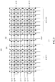
- Figure 1 shows a circuit diagram of an existing memory array 100.
- the memory array 100 includes a plurality of memory columns.
- the memory cells in the memory columns are flash memory cells.
- the drains of the memory cells in each columns of the memory array 100 are coupled to the bit lines corresponding to the memory columns, such as the bit lines b1 ⁇ 0>, b1 ⁇ 1> whil b1 ⁇ 190>, and b1 ⁇ 191> illustrated in Figure 1 .
- the control gates of the m th rows of flash memory cells in the plurality of memory columns are coupled to the control gates of the (m+1) th rows of flash memory cells in the plurality of memory columns; and coupled to the corresponding control gate lines, such as control gate lines cg ⁇ 0> and cg ⁇ 1> illustrated in Figure 1 .
- the sources of the m th rows of flash memory cells in the plurality of memory columns and the sources of the (m+1) th rows of flash memory cells in the plurality of memory columns are configured to receive the source line signals, such as source line signals s1 ⁇ 0> and s1 ⁇ 1> illustrated in Figure 1 .
- select gates of the flash memory cells in a same row of memory cells in the plurality of memory columns are respectively coupled to a same work line, such as work lines w1 ⁇ 0>, w1 ⁇ 1>, w1 ⁇ 2> and w1 ⁇ 3>, where m ⁇ 1; and m is an odd number.
- the source of a to-be-read flash memory cell 10 in the memory array 100 needs to be pulled down to a potential of 0 V.
- the existing technologies often utilize relatively large pull down devices, such as NMOS transistors including the pull down devices 20, 30, 40, and 50, to couple the source of the to-be-read flash memory cell 10.
- the pull down signal slpd ⁇ 0> turns on the pull down devices 20 and 30 to pull down the source of the to-be-read flash memory cell 10 to ground, i.e., a potential of 0 V relative to the ground. If the to-be-read flash memory cell is in the third row or the fourth row of the memory array 100, the pull down devices 40 and 50 are turned on by the pull down signal slpd ⁇ 1> to pull down the source of the to-be-read flash memory 10.
- the paths between the source of the to-be-read flash memory cell 10 in the memory cell array 100 and the pull down devices have certain impedances. Specifically, the paths have metal resistors and diffusion resistors. Thus, in reality, the potential of the source of the to-be-read flash memory is not 0 V. Such a condition significantly affects the reading performance of the to-be-read flash memory cell 10. Especially when the number of the columns in the memory array 100 is relatively large, the impedance issue is more severe; and the reading performance of the flash memory cell is worse.
- Figure 2 illustrates a schematic of the equivalent resistors between the to-be-read flash memory cell 10 and the pull down devices in the existing memory array 100.
- the source of the to-be read flash memory cell 10 outputs a source current I sl .
- the paths for the source current I sl flowing into the put down device 20 and the pull down device 30 can be equivalent to metal resistors RM_L, RM_M and RM_R, and diffusion resistors Rdiff_L and Rdiff_R.
- the existing technologies often connect the metal resistors and the diffusion resistors with the other resistors in parallel to reduce the resistances of the metal resistors and the diffusion resistors in the circuit.
- the resistors R1, R2, R3 and R4 are connected in the circuit. Connecting the resistors in parallel is able to reduce the resistances of the metal resistors and the diffusion resistors in the circuit to a certain extent; and cause the potential of the sources of the flash memory cell 10 to be closer to 0 V to improve the reading performance of the flash memory cell 10.
- the improvement of the reading performance of the flash memory cell 10 has a certain limitation. Further, extra mask areas are needed in the circuit design; and the power consumption of the memory array 100 is increased.
- a first aspect of the present invention provides a memory array.
- the memory array includes a plurality of memory columns. Each memory column has a plurality of flash memory cells, and the memory columns are divided into at least two blocks. At least one source pull down column is disposed between two adjacent blocks; and each source pull down column has a plurality of flash memory cells.
- a select gate of each flash memory cell in the source pull down column and select gates of the corresponding flash memory cells of the plurality of memory columns in a same row are coupled to a same word line; a control gate of each flash memory cell in the source pull down column and control gates of the corresponding flash memory cells of the plurality of memory columns in a same row are coupled to a same control gate line; an erasing gate of each flash memory cell in the source pull down column and erasing gates of the corresponding flash memory cells of the plurality of memory columns in a same row are coupled to a same erasing gate line; and a source of each flash memory cell in the source pull down column is coupled to sources of the corresponding flash memory cells of the plurality of memory columns in a same row; and a drain of each flash memory cell in the source pull down column is configured to receive a source pull down control signal.
- drains of each column of flash memory cells are coupled to a word line corresponding to the column of flash memory cells.
- control gates of an mth column of flash memory cells are mutually coupled with control gates of an (m+1)th column of flash memory cells and coupled to a corresponding control gate line.
- erasing gates of the mth column of flash memory cells are mutually coupled with erasing gates of the (m+1)th column of flash memory cells and coupled to a corresponding erasing gate line.
- sources of the mth column of flash memory cells and sources of the (m+1)th column of flash memory cells are configured to received source line signals, wherein: m ⁇ 1; and m is an odd number.
- a number of the plurality of memory columns is a positive integral time of 8.
- a number of the memory columns in each block is a positive integral power of 2.
- the number of the memory columns in each block is 8; and two source pull down columns are disposed between two adjacent blocks.
- the flash memory cells are stacked gate flash memory cells.
- a second aspect of the present invention provides a method for reading a memory array.
- the method includes providing a memory array having a plurality of memory columns. Each memory column has a plurality of flash memory cells; and the memory columns are divided into at least two blocks. At least one source pull down column is disposed between the two adjacent blocks; and each source pull down column has a plurality of flash memory cells. A select gate of each flash memory cell in the source pull down column and select gates of the corresponding flash memory cells of the plurality of memory columns in a same row are coupled to a same word line. A control gate of each flash memory cell in the source pull down column and control gates of the corresponding flash memory cells of the plurality of memory columns in a same row are coupled to a same control gate line.
- An erasing gate of each flash memory cell in the source pull down column and erasing gates of the corresponding flash memory cells of the plurality of memory columns in a same row are coupled to a same erasing gate line.
- a source of each flash memory cell in the source pull down column are coupled to sources of the corresponding flash memory cells of the plurality of memory columns in a same row.
- a drain of each flash memory cell in the source pull down column is configured to receive a source pull down control signal.
- the method also includes controlling the source pull down control signal to be approximately 0 V; and setting voltages of the word line, the bit line, the control gate line and the erasing gate line coupled to a selected flash memory cell to cause the selected flash memory cell to be read.
- setting voltages of the word line, the bit line, the control gate line and the erasing gate line coupled to the selected flash memory cell comprises: applying a first voltage to the bit line coupled to the selected flash memory cell; applying a second voltage to the word line coupled to the selected flash memory cell; applying a third voltage to the control gate line coupled to the selected flash memory cell; and applying a fourth voltage to the erasing gate line coupled to the selected flash memory cell.
- the first voltage is in a range of approximately 0.5 V-1 V. Most preferably, the first voltage is approximately 0.7 V.
- the second voltage is in a range of approximately 2 V-3 V. Most preferably, the second voltage is approximately 2.5 V.
- the third voltage is in a range of approximately 2 V-3 V. Most preferably, the third voltage is approximately 2.5 V.
- the fourth voltage is approximately 0 V.
- the method further comprises: setting a source signal received by the source of the selected flash memory cell to be approximately 0 V.
- setting the source signal received by the source of the selected flash memory cell to be approximately 0 V comprises: obtaining the source signal by decoding an operation mode of the memory array.
- setting the source signal received by the source of the selected flash memory cell to be approximately 0 V comprises: pulling down the source of the selected flash memory cell by a relatively small pull down device.
- a third aspect of the present invention provides a programming method of a memory array according to the first aspect.
- the programming method comprises, the method further comprises: setting voltages of the pull down control signal, the word line, the bit line, the control gate line and the erasing gate line coupled to a selected flash memory cell to cause the selected flash memory cell to be programmed, and cause the flash memory cells of the pull down memory column not to be programed.
- setting voltages of the pull down control signal, the word line, the bit line, the control gate line and the erasing gate line comprises: controlling the pull down control signal to be in a range of approximately 2 V-3 V, most preferably approximately 2.5 V; applying a voltage in a range of approximately 0.1 V-0.5 V, most preferably 0.3 V, to the bit line coupled to the selected flash memory cell; applying a voltage in a range of approximately 0.8 V-1.2 V, most preferably 1 V, to the word line coupled to the selected flash memory cell; applying a voltage in a range of approximately 10 V-11 V, most preferably 10.5 V, to the control gate line coupled to the selected flash memory cell; and applying a voltage in a range of approximately 4 V-5 V, most preferably, 4.5 V, to the erasing gate line coupled to the selected flash memory cell.
- the voltage applied to the pull down control signal is approximately 2.5 V; the voltage applied to the bit line coupled to the selected flash memory cell is approximately 0.3 V; the voltage applied to the word line coupled to the selected flash memory cell is approximately 1 V; the voltage applied to the control gate line coupled to the selected flash memory cell is approximately 10.5 V; and the voltage applied to the erasing gate line coupled to the selected flash memory cell is approximately 4.5 V.
- the method further comprises: setting a source signal received by the source of the selected flash memory cell to be approximately 2.5 V.
- a fourth aspect of the present invention provides an erasing method of the memory array according to the first aspect.
- the erasing method comprises: setting voltages of the pull down control signal, the word line, the bit line, the control gate line and the erasing gate line coupled to a selected flash memory cell to cause the selected flash memory cell and the flash memory in the source pull down column all to be erased.
- setting voltages of the pull down control signal, the word line, the bit line, the control gate line and the erasing gate line comprises: controlling the pull down control signal to be approximately 0 V; applying a voltage of approximately 0 V to the bit line coupled to the selected flash memory cell; applying a voltage of approximately 0 V to the word line coupled to the selected flash memory cell; applying a voltage of approximately 0 V to the control gate line coupled to the selected flash memory cell; and applying a voltage in a range of approximately 11 V-12 V, most preferably 11.5 V, to the erasing gate line coupled to the selected flash memory cell.
- the voltage applied to the erasing gate line coupled to the selected flash memory cell is approximately 11.5 V.
- a method for reading a memory array according to the second aspect of the present invention, a method for programming a memory array according to the third aspect of the present invention and a method for erasing a memory array according to the fourth aspect of the present invention is particularly useful in connection with a memory array according to the first aspect of the present invention.
- the present invention provides memory arrays and reading, programming and erasing methods of the memory array.
- the memory array may include a plurality of memory columns.
- the plurality of memory columns may be divided into at least two blocks; and at least one source pull down column may be disposed between two adjacent blocks.
- the source pull down column may include a plurality of flash memory cells.
- the select gate of each flash memory cell in the source pull down column and the select gates of the corresponding flash memory cells of the plurality of memory columns in a same row may be coupled to a same word line.
- the control gate of each flash memory cell in the source pull down column and the control gate of the corresponding flash memory cells of the plurality of memory columns in a same row may be coupled to a same control gate line.
- the erasing gate of each flash memory cell in the source pull down column and the corresponding erasing gates of the flash memory cells in the plurality of memory columns in a same row may be coupled to a same erasing gate line.
- the source of each flash memory cell in the source pull down column may be coupled to the sources of the corresponding flash memory cells in the plurality of memory columns in a same row.
- the drain of each flash memory cell in the source pull down column may be configured to receive the pull down control signal.
- Figure 3 illustrates a circuit diagram of an exemplary memory array 200 consistent with the disclosed embodiments.
- the memory array 200 may include a plurality of memory columns.
- Each memory column may include a plurality of flash memory cells.
- the memory array 200 includes 4 rows and 16 columns.
- the memory array may have any other appropriate size; and the size of the memory array is not limited.
- the plurality of memory columns may be divided into at least two blocks.
- a source pull down column 202 may be disposed between two adjacent blocks.
- the source pull down column 202 may have a plurality of flash memory cells.
- the select gate of each flash memory cell in the source pull down column 202 and the select gates of the corresponding flash memory cells in the plurality of memory columns in a same row as the flash memory cell in the source pull down column 202 may be coupled to a same word line, such as the word lines wl ⁇ 0>, wl ⁇ 1>, wl ⁇ 2> and wl ⁇ 3> illustrated in Figure 3 .
- the control gate of each flash memory cell in the source pull down column 202 and the control gates of the corresponding flash memory cells of the plurality of the memory columns in a same row as the flash memory cell in the source pull down column 202 may be coupled to a same control gate line, such as the word lines cg ⁇ 0> and cg ⁇ 1> illustrated in Figure 3 .
- the erasing gate of each flash memory cell in the source pull down column 202 and the erasing gates of the corresponding flash memory cells of the plurality of the memory columns in a same row as the flash memory cell in the source pull down column 202 may be coupled to a same erasing gate line (not shown).
- the source of each flash memory cell in the source pull down column 202 may be coupled to the sources of the corresponding flash memory cells of the plurality of the memory columns in a same row as the flash memory cell in the source pull down column 202.
- the drain of each flash memory cell in the source pull down column 202 may be configured to receive a pull down control signal of a selected (to-be-read memory cell) 201.
- the flash memory cells may be any appropriate type.
- the flash memory cells are stacked gate flash memory cells.
- the pull down control signal may be generated by a coding circuit (not shown).
- the coding source and the coding methods are not limited. Different pull down control signals may be obtained by coding processes according to the operation requirements of the memory array 200, such as reading, programming, and erasing, etc.
- the source pull down column 202 may be disposed between adjacent blocks of the memory array 200.
- the pull down signal "blpd" may be controlled as 0 V.
- the configurations of the word lines, control gate lines and erasing lines of a selected (to-be-read) flash memory cell 201 in the memory array 200 may turn on the source and the drain of a corresponding flash memory cell in the source pull down column 202 in a same row.
- the pull down control signal is 0 V
- the source of the selected flash memory 201 may be pulled down to a zero potential by the source pull down column to cooperate with the reading operation of the selected flash memory 201.
- the memory array 200 may have a plurality of source pull down columns 202. Comparing with the existing technologies, the memory array 200 may be able to reduce the pulled down paths of the source of the selected flash memory cell 201 by controlling the pull down control signal "blpd". Accordingly, the metal resistance and the diffusion resistance in the pulled down paths of the source of the selected flash memory cell 201 may be reduced. Therefore, comparing with the existing technologies, the real potential of the source of the selected flash memory cell 201 may be closer to 0 V. Accordingly, the reading performance of the memory array 200 may be improved.
- the number of the memory columns may be a positive integral time of 8 (e.g., 8n, where n is a positive integer).
- the memory array may include 192 memory columns. The number of the memory columns of the memory array is not limited.
- the number of the blocks in the memory array may be a positive integral time of power of 2 (2 n , where n is a positive integer).
- the number of blocks in the memory array may be 2, 4, 8, 16, etc.
- each block of the memory array 200 may include 8 memory columns; and 2 source pull down columns may be disposed between adjacent blocks. That is, in the memory array 200, 2 source pull down columns may be disposed between adjacent 8 memory columns.
- the source pull down column 202 may be used to form an optimized pull down path for the source of the selected flash memory cell 201; and the source pull down column 202 may not be operated along with the selected flash memory cell 201. Thus, the insertion of the source pull down column 202 may separate the plurality of memory columns of the memory array 200.
- a constant number of source pull down memory columns 202 may be inserted between adjacent memory columns according to a certain regularity to cause the operation of the memory array 200 inserted with the pull down memory columns 202 to have certain regularity and continuity. Accordingly, it may enable the design of the circuit and the controlling of the controllers to be convenient.
- the smaller the sizes of the blocks are the closer the sources of the to-be-read flash memory 201 are pulled down to the ground through the source pull down columns 202. Accordingly, the equivalent resistance in the pull down paths may be smaller.
- the larger the number of the source pull down columns 202 is the smaller of the diffusion resistances in the pull down paths are. That is, the smaller the size of the blocks is, the larger the number of the source pull down columns 202 inserted between the adjacent blocks is.
- the source of the selected flash memory cell 201 may be pulled down closer to the 0 V potential. Accordingly, the reading operation of the memory cell 200 may be better improved.
- the sizes of the blocks and the number of the source pull down columns 202 may be adjusted according to other factors, such as the area of the memory array 200, and the power of the memory array 200, etc.
- the source pull down column 202 may include a plurality of flash memory cells.
- the flash memory cells of the source pull down columns 202 may be identical to the flash memory cells of the memory columns.
- all the flash memory cells in the memory array 200 may be coherent; and such a design may be easy to realize.
- the memory array 200 when operated, it may only need to set the pull down control signal "blpd"; and the operation may be relatively simple.
- the disclosed memory array 200 may not use relatively large size pull down devices; and may utilize the source pull down column 202 to pull down the source of the selected flash memory cell 201.
- the area of the mask for fabricating the memory array 200 may be significantly reduced.
- the memory array 200 may have 4 columns and 16 columns. In specific embodiments, the size of the memory array may be expanded.
- the drains of the flash memory cells in each column of the memory array 200 may be coupled to the corresponding bit lines, such as the bit lines b1 ⁇ 8:7> and b1 ⁇ 8:15> illustrated in Figure 3 .
- the control gates of the flash memory cells in the m th row of the plurality of memory columns may be mutually coupled to the control gates of the flash memory cells in the (m+1) th row of the plurality of memory columns, and together coupled to the corresponding control gate lines, such as the control gate lines cg ⁇ 0> and cg ⁇ 1> illustrated in Figure 3 .
- the erasing gates of the flash memory cells in the m th row of the plurality of memory columns may be mutually coupled to the erasing gates of the flash memory cells in the (m+1)th row of plurality of memory columns, and together coupled to the corresponding erasing gate lines (not shown).
- the sources of the flash memory cells in the m th row of the plurality of memory columns and the sources of the flash memory cells in the (m+1) th row of plurality of memory columns may receive source line signals, such as the source line signals sl ⁇ 0> and sl ⁇ 1> illustrated in Figure 3 .
- the select gates of the flash memory cells in a same row of the plurality of memory columns may be coupled to a same word line, such as the word lines wl ⁇ 0>, wl ⁇ 1>, wl ⁇ 2> and wl ⁇ 3>, where m ⁇ 1; and m is an odd number.
- the memory array 200 inserted with the source pull down column 202 may be operated by controlling the pull down control signal "blpd" according to different operation modes.
- Figure 4 illustrates an exemplary reading method of a memory array consistent with the disclosed embodiments.
- the reading method may be used to perform a reading operation to the memory array 200 illustrated in Figure 3 , or other appropriate memory arrays. For illustrative purposes, the reading operation of the memory array 200 is described.
- the reading method may include controlling the pull down signal "blpd" to be 0 V (S101). Further, the reading method may include setting the voltages of the bit line, the word line, the control gate line and the erasing gate line coupled to a selected flash memory cell to cause the selected flash memory cell, such as the flash memory cell 201, to be read (S102). Under such a condition, the flash memory cell of the source pull down column 202 in a same row as the selected flash memory cell 201 may be turned on. Turning on such a flash memory cell may aid to pull down the source of the selected flash memory cell 201 to be 0 V potential.
- setting the voltages of the bit line, the word line, the control gate line and the erasing gate line coupled to the selected flash memory cell 201 may include applying a first voltage to the bit line coupled to the selected flash memory cell 201; applying a second voltage to the word line coupled to the selected flash memory cell 201; applying a third voltage to the control gate line coupled to the selected flash memory cell 201; and applying a fourth voltage to the erasing gate line coupled to the selected flash memory 201.
- the first voltage may be in range of approximately 0.5 V-1.0 V. In one embodiment, the first voltage is approximately 0.7 V.
- the second voltage may be in a range of approximately 2.0 V-3.0 V. In one embodiment, the second voltage is approximately 2.5 V.
- the third voltage may be in a range of approximately 2.0 V-3.0 V. In one embodiment, the third voltage is approximately 2.5 V.
- the fourth voltage may be approximately 0 V.
- the reading method may also include setting the source line signal sl ⁇ 0> as 0V (the source line signal received by the source of the flash memory cell 201 is sl ⁇ 0>) (S103).
- the source line signal sl ⁇ 0> may be obtained by decoding the operation mode of the memory array 200.
- the source line signal sl ⁇ 0> may also be obtained by pulled down the source line signal sl ⁇ 0> to ground by a relatively small pull down device.
- the present invention also provides a programming method of a memory array.
- the programming method may be used to perform a programing operation to the memory array 200 illustrated in Figure 3 , or other appropriate memory arrays.
- the programming operation of the memory array 200 is described herein.
- the programming method may include setting the voltages of the bit line, the word line, the control gate line and the erasing gate line coupled to a certain selected (to-be-read) flash memory cell to cause the certain flash memory cell, such as the flash memory cell 201, to be programmed; and controlling the pull down control signal "blpd" to cause the flash memory cells of the pull down column 202 not to be programed.
- controlling the pull down control signal “blpd” may include controlling the pull down control signal “blpd” to be in a range approximately 2 V-3 V.
- Setting the voltages of the bit line, the word line, the control gate line and the erasing gate line coupled to the selected flash memory cell 201 may include applying a voltage in a range of approximately 0.1 V-0.5 V to the bit line coupled to the selected memory cell 201; applying a voltage in a range of approximately 0.8 V-1.2 V to the word line coupled to the selected flash memory cell 201; applying a voltage in a range of approximately 10 V-11 V to the control gate line coupled to the selected flash memory cell 201; and applying a voltage in a range of approximately 4 V-5 V to the erasing gate line coupled to the selected flash memory cell 201.
- the pull down control signal may be controlled as approximately 2.5 V.
- the voltage applied to the bit line coupled to the selected flash memory cell 201 is approximately 0.3 V; the voltage applied to the word line coupled to the selected flash memory cell 201 is approximately 1 V; the voltage applied to the control gate line coupled to the selected flash memory cell 201 is in a range of approximately 10.5 V; and the voltage applied to the erasing gate line coupled to the selected flash memory 201 is approximately 4.5 V.
- the programing method may also include setting source line signal sl ⁇ 0> as approximately 2.5 V.
- the source line signal sl ⁇ 0> may be obtained by decoding the operation modes of the memory array 200.
- the present invention also provides an erasing method of a memory array.
- the erasing method may be used to perform an erasing operation to the memory array 200 illustrated in Figure 3 , or other appropriate memory arrays. For illustrative purposes, the erasing operation of the memory array 200 is described.
- the erasing method may include setting the voltages of the bit line, the word line, the control gate line and the erasing gate line coupled to a certain selected (to-be-read) flash memory cell to cause the certain flash memory cell, such as the flash memory cell 201, to be erased; and also setting the pull down control signal "blpd" to cause the flash memory cells of the pull down column 202 to be erased.
- setting the pull down control signal "blpd” may include controlling the pull down control signal “blpd” to be approximately 0 V.
- Setting the voltages of the bit line, the word line, the control gate line and the erasing gate line coupled to the selected flash memory cell 201 may include applying a voltage of approximately 0 V to the bit line coupled to the selected flash memory cell 201; applying a voltage of 0 V to the word line coupled to the selected flash memory cell 201; applying a voltage approximately 0 V to the control gate line coupled to the selected flash memory cell 201; and applying a voltage in a range of approximately 11 V-12 V to the erasing gate line coupled to the selected flash memory 201.
- the pull down control signal may be controlled as approximately 0 V.
- the voltage applied to the bit line coupled to the selected flash memory cell 201 is approximately 0 V; the voltage applied to the word line coupled to the selected flash memory cell 201 is approximately 0 V; the voltage applied to the control gate line coupled to the selected flash memory cell 201 is approximately 0 V; and the voltage applied to the erasing gate line coupled to the t selected flash memory 201 is approximately 11.5 V.
- the programing method may also include setting source line signal s1 ⁇ 0> as approximately 0 V.
- the source line signal sl ⁇ 0> may be obtained by decoding the operation modes of the memory array 200.
- the source line signal sl ⁇ 0> may also be obtained by pulled down the source line signal sl ⁇ 0> to ground by a relatively small pull down device.
- the reading, programming and erasing methods of the memory array 200 may not be limited.
- the voltages applied to each terminals of the flash memory cells are referred to the voltages relative to the ground of the memory array 200.
- the pull down control signal when the disclosed memory array is performing a reading operation, the pull down control signal may be controlled to be 0 V. Further, the voltage setups of the word line, the control gate line, and the control gate line of the selected (to-be-read) flash memory cell may turn on the source-drain of a flash memory cell of the source pull down memory column in a same row as the selected flash memory cell. Thus, when the pull down control signal is controlled to be 0 V, the source of the flash memory cell in the source pull down memory column may be pulled to a zero potential to cooperate of the reading operation of the selected flash memory cell. Because at least one source pull down column may be disposed between adjacent blocks, the memory array may have a plurality of source pull down columns.
- the disclosed memory array may reduce the pulled down path of the source of the selected flash memory cell by controlling the source pull down signal. Accordingly, the metal resistance and the diffusion resistance in the pulled down path of the selected flash memory cell may be reduced. Therefore, comparing with the existing technologies, the real potential of the source of the selected flash memory cell may be closer to 0 V. Accordingly, the reading performance of the memory array may be improved.
- the source pull down columns may include a plurality of flash memory cells.
- the flash memory cells of the source pull down columns may be identical to the flash memory cells of the memory column.
- all the flash memory cells in the memory array may be coherent; and such a design may be easy to realize.
- the memory array when operated, it may only need to set the pull down control signal; and the operation may be relatively simple.
- the disclosed memory array may not use relatively large pull down devices; and may use the source pull down column to pull down the source of the selected flash memory cell.
- the area of the mask for forming the memory array may be significantly reduced.
Landscapes
- Engineering & Computer Science (AREA)
- Microelectronics & Electronic Packaging (AREA)
- Computer Hardware Design (AREA)
- Read Only Memory (AREA)
- Non-Volatile Memory (AREA)
Description
- This application claims the priority of Chinese patent application No.
201610788897.8, filed on August 31, 2016 - The present invention generally relates to the field of memory and, more particularly, relates to memory arrays, and reading, programming and erasing methods thereof.
- Flash memory is a type of long life span, non-volatile memory. The flash memory may maintain stored data information, even when the power is off. As such, the flash memory is often used to store configuration information. For example, data may be stored in the basic input output system (BIOS) of personal computers, personal digital assistant (PDA), and digital cameras, etc.
-
Figure 1 shows a circuit diagram of anexisting memory array 100. As shown inFigure 1 , taking a 4-row and 192-column memory array as an example, thememory array 100 includes a plurality of memory columns. The memory cells in the memory columns are flash memory cells. The drains of the memory cells in each columns of thememory array 100 are coupled to the bit lines corresponding to the memory columns, such as the bit lines b1<0>, b1<1>...... b1<190>, and b1<191> illustrated inFigure 1 . The control gates of the mth rows of flash memory cells in the plurality of memory columns are coupled to the control gates of the (m+1)th rows of flash memory cells in the plurality of memory columns; and coupled to the corresponding control gate lines, such as control gate lines cg<0> and cg<1> illustrated inFigure 1 . The sources of the mth rows of flash memory cells in the plurality of memory columns and the sources of the (m+1)th rows of flash memory cells in the plurality of memory columns are configured to receive the source line signals, such as source line signals s1<0> and s1<1> illustrated inFigure 1 . Further, the select gates of the flash memory cells in a same row of memory cells in the plurality of memory columns are respectively coupled to a same work line, such as work lines w1<0>, w1<1>, w1<2> and w1<3>, where m≥1; and m is an odd number. - During the reading operation of the
memory array 100, the source of a to-be-readflash memory cell 10 in thememory array 100 needs to be pulled down to a potential of 0 V. The existing technologies often utilize relatively large pull down devices, such as NMOS transistors including the pull downdevices flash memory cell 10. Further, the pull down signal slpd<0> turns on the pull downdevices flash memory cell 10 to ground, i.e., a potential of 0 V relative to the ground. If the to-be-read flash memory cell is in the third row or the fourth row of thememory array 100, the pull downdevices be-read flash memory 10. - However, the paths between the source of the to-be-read
flash memory cell 10 in thememory cell array 100 and the pull down devices have certain impedances. Specifically, the paths have metal resistors and diffusion resistors. Thus, in reality, the potential of the source of the to-be-read flash memory is not 0 V. Such a condition significantly affects the reading performance of the to-be-readflash memory cell 10. Especially when the number of the columns in thememory array 100 is relatively large, the impedance issue is more severe; and the reading performance of the flash memory cell is worse. -
Figure 2 illustrates a schematic of the equivalent resistors between the to-be-readflash memory cell 10 and the pull down devices in theexisting memory array 100. As shown inFigure 2 , the source of the to-be readflash memory cell 10 outputs a source current Isl. The paths for the source current Isl flowing into the put downdevice 20 and the pull downdevice 30 can be equivalent to metal resistors RM_L, RM_M and RM_R, and diffusion resistors Rdiff_L and Rdiff_R. The existing technologies often connect the metal resistors and the diffusion resistors with the other resistors in parallel to reduce the resistances of the metal resistors and the diffusion resistors in the circuit. Specifically, as shown inFigure 2 , the resistors R1, R2, R3 and R4 are connected in the circuit. Connecting the resistors in parallel is able to reduce the resistances of the metal resistors and the diffusion resistors in the circuit to a certain extent; and cause the potential of the sources of theflash memory cell 10 to be closer to 0 V to improve the reading performance of theflash memory cell 10. However, the improvement of the reading performance of theflash memory cell 10 has a certain limitation. Further, extra mask areas are needed in the circuit design; and the power consumption of thememory array 100 is increased. - Therefore, the existing memory arrays still have the reading performance issues.
- It is an object oft he present invention to provide a memory array structure, and memory reading, programming and erasing methods which may solve one or more problems set forth above and other problems in the art, in particular by which the above discussed reading performance issues may be avoided or at least reduced so that an improved reading performance may be achieved.
- The object is achieved by the features of the respective independent claims. Further embodiments are defined in the respective dependent claims.
- A first aspect of the present invention provides a memory array.
- The memory array includes a plurality of memory columns. Each memory column has a plurality of flash memory cells, and the memory columns are divided into at least two blocks. At least one source pull down column is disposed between two adjacent blocks; and each source pull down column has a plurality of flash memory cells. A select gate of each flash memory cell in the source pull down column and select gates of the corresponding flash memory cells of the plurality of memory columns in a same row are coupled to a same word line; a control gate of each flash memory cell in the source pull down column and control gates of the corresponding flash memory cells of the plurality of memory columns in a same row are coupled to a same control gate line; an erasing gate of each flash memory cell in the source pull down column and erasing gates of the corresponding flash memory cells of the plurality of memory columns in a same row are coupled to a same erasing gate line; and a source of each flash memory cell in the source pull down column is coupled to sources of the corresponding flash memory cells of the plurality of memory columns in a same row; and a drain of each flash memory cell in the source pull down column is configured to receive a source pull down control signal.
- Preferably, drains of each column of flash memory cells are coupled to a word line corresponding to the column of flash memory cells. Preferably, control gates of an mth column of flash memory cells are mutually coupled with control gates of an (m+1)th column of flash memory cells and coupled to a corresponding control gate line. Preferably, erasing gates of the mth column of flash memory cells are mutually coupled with erasing gates of the (m+1)th column of flash memory cells and coupled to a corresponding erasing gate line. Preferably, sources of the mth column of flash memory cells and sources of the (m+1)th column of flash memory cells are configured to received source line signals, wherein: m≥1; and m is an odd number.
- Preferably, a number of the plurality of memory columns is a positive integral time of 8.
- Preferably, a number of the memory columns in each block is a positive integral power of 2.
- Preferably, the number of the memory columns in each block is 8; and two source pull down columns are disposed between two adjacent blocks.
- Preferably, the flash memory cells are stacked gate flash memory cells.
- A second aspect of the present invention provides a method for reading a memory array.
- The method includes providing a memory array having a plurality of memory columns. Each memory column has a plurality of flash memory cells; and the memory columns are divided into at least two blocks. At least one source pull down column is disposed between the two adjacent blocks; and each source pull down column has a plurality of flash memory cells. A select gate of each flash memory cell in the source pull down column and select gates of the corresponding flash memory cells of the plurality of memory columns in a same row are coupled to a same word line. A control gate of each flash memory cell in the source pull down column and control gates of the corresponding flash memory cells of the plurality of memory columns in a same row are coupled to a same control gate line. An erasing gate of each flash memory cell in the source pull down column and erasing gates of the corresponding flash memory cells of the plurality of memory columns in a same row are coupled to a same erasing gate line. A source of each flash memory cell in the source pull down column are coupled to sources of the corresponding flash memory cells of the plurality of memory columns in a same row. A drain of each flash memory cell in the source pull down column is configured to receive a source pull down control signal. The method also includes controlling the source pull down control signal to be approximately 0 V; and setting voltages of the word line, the bit line, the control gate line and the erasing gate line coupled to a selected flash memory cell to cause the selected flash memory cell to be read.
- Preferably, setting voltages of the word line, the bit line, the control gate line and the erasing gate line coupled to the selected flash memory cell comprises: applying a first voltage to the bit line coupled to the selected flash memory cell; applying a second voltage to the word line coupled to the selected flash memory cell; applying a third voltage to the control gate line coupled to the selected flash memory cell; and applying a fourth voltage to the erasing gate line coupled to the selected flash memory cell.
- Preferably, the first voltage is in a range of approximately 0.5 V-1 V. Most preferably, the first voltage is approximately 0.7 V.
- Preferably, the second voltage is in a range of approximately 2 V-3 V. Most preferably, the second voltage is approximately 2.5 V.
- Preferably, the third voltage is in a range of approximately 2 V-3 V. Most preferably, the third voltage is approximately 2.5 V.
- Preferably, the fourth voltage is approximately 0 V.
- Preferably, the method further comprises: setting a source signal received by the source of the selected flash memory cell to be approximately 0 V.
- Preferably, setting the source signal received by the source of the selected flash memory cell to be approximately 0 V comprises: obtaining the source signal by decoding an operation mode of the memory array.
- Preferably, setting the source signal received by the source of the selected flash memory cell to be approximately 0 V comprises: pulling down the source of the selected flash memory cell by a relatively small pull down device.
- A third aspect of the present invention provides a programming method of a memory array according to the first aspect.
- The programming method comprises, the method further comprises: setting voltages of the pull down control signal, the word line, the bit line, the control gate line and the erasing gate line coupled to a selected flash memory cell to cause the selected flash memory cell to be programmed, and cause the flash memory cells of the pull down memory column not to be programed.
- Preferably, setting voltages of the pull down control signal, the word line, the bit line, the control gate line and the erasing gate line comprises: controlling the pull down control signal to be in a range of approximately 2 V-3 V, most preferably approximately 2.5 V; applying a voltage in a range of approximately 0.1 V-0.5 V, most preferably 0.3 V, to the bit line coupled to the selected flash memory cell; applying a voltage in a range of approximately 0.8 V-1.2 V, most preferably 1 V, to the word line coupled to the selected flash memory cell; applying a voltage in a range of approximately 10 V-11 V, most preferably 10.5 V, to the control gate line coupled to the selected flash memory cell; and applying a voltage in a range of approximately 4 V-5 V, most preferably, 4.5 V, to the erasing gate line coupled to the selected flash memory cell. That is to say, most preferably, the voltage applied to the pull down control signal is approximately 2.5 V; the voltage applied to the bit line coupled to the selected flash memory cell is approximately 0.3 V; the voltage applied to the word line coupled to the selected flash memory cell is approximately 1 V; the voltage applied to the control gate line coupled to the selected flash memory cell is approximately 10.5 V; and the voltage applied to the erasing gate line coupled to the selected flash memory cell is approximately 4.5 V.
- Preferably, the method further comprises: setting a source signal received by the source of the selected flash memory cell to be approximately 2.5 V.
- A fourth aspect of the present invention provides an erasing method of the memory array according to the first aspect.
- The erasing method comprises: setting voltages of the pull down control signal, the word line, the bit line, the control gate line and the erasing gate line coupled to a selected flash memory cell to cause the selected flash memory cell and the flash memory in the source pull down column all to be erased.
- Preferably, setting voltages of the pull down control signal, the word line, the bit line, the control gate line and the erasing gate line comprises: controlling the pull down control signal to be approximately 0 V; applying a voltage of approximately 0 V to the bit line coupled to the selected flash memory cell; applying a voltage of approximately 0 V to the word line coupled to the selected flash memory cell; applying a voltage of approximately 0 V to the control gate line coupled to the selected flash memory cell; and applying a voltage in a range of approximately 11 V-12 V, most preferably 11.5 V, to the erasing gate line coupled to the selected flash memory cell. In other words, most preferably, the voltage applied to the erasing gate line coupled to the selected flash memory cell is approximately 11.5 V.
- A method for reading a memory array according to the second aspect of the present invention, a method for programming a memory array according to the third aspect of the present invention and a method for erasing a memory array according to the fourth aspect of the present invention is particularly useful in connection with a memory array according to the first aspect of the present invention.
- Other aspects of the present invention can be understood by those skilled in the art in light of the description, the claims, and the drawings of the present invention.
-
-
Figure 1 illustrates a circuit diagram of an existing memory array; -
Figure 2 illustrates a schematic of equivalent resistors of the paths between the source of the selected flash memory and the pull down devices in the existingmemory array 100 illustrated inFigure 1 ; -
Figure 3 illustrates a circuit diagram of an exemplary memory array consistent with the disclosed embodiments; and -
Figure 4 illustrates an exemplary memory array reading method consistent with the disclosed embodiments. - Reference will now be made in detail to exemplary embodiments of the disclosure, which are illustrated in the accompanying drawings. Wherever possible, the same reference numbers will be used throughout the drawings to refer to the same or like parts.
- The present invention provides memory arrays and reading, programming and erasing methods of the memory array.
- The memory array may include a plurality of memory columns. The plurality of memory columns may be divided into at least two blocks; and at least one source pull down column may be disposed between two adjacent blocks. The source pull down column may include a plurality of flash memory cells. The select gate of each flash memory cell in the source pull down column and the select gates of the corresponding flash memory cells of the plurality of memory columns in a same row may be coupled to a same word line. The control gate of each flash memory cell in the source pull down column and the control gate of the corresponding flash memory cells of the plurality of memory columns in a same row may be coupled to a same control gate line. The erasing gate of each flash memory cell in the source pull down column and the corresponding erasing gates of the flash memory cells in the plurality of memory columns in a same row may be coupled to a same erasing gate line. The source of each flash memory cell in the source pull down column may be coupled to the sources of the corresponding flash memory cells in the plurality of memory columns in a same row. The drain of each flash memory cell in the source pull down column may be configured to receive the pull down control signal. By the controlling of the pull down control signal, the pull down path of the source of a selected (to-be-read) flash memory cell in the memory array may be reduced. Thus, the reading performance of the flash memory cell may be improved; and the circuit design may be easier to realize. Further, the mask area for fabricating the flash memory array may be saved.
-
Figure 3 illustrates a circuit diagram of anexemplary memory array 200 consistent with the disclosed embodiments. As shown inFigure 3 , thememory array 200 may include a plurality of memory columns. Each memory column may include a plurality of flash memory cells. - For illustrative purposes, the
memory array 200 includes 4 rows and 16 columns. In some embodiments, the memory array may have any other appropriate size; and the size of the memory array is not limited. - The plurality of memory columns may be divided into at least two blocks. A source pull down
column 202 may be disposed between two adjacent blocks. The source pull downcolumn 202 may have a plurality of flash memory cells. - The select gate of each flash memory cell in the source pull down
column 202 and the select gates of the corresponding flash memory cells in the plurality of memory columns in a same row as the flash memory cell in the source pull downcolumn 202 may be coupled to a same word line, such as the word lines wl<0>, wl<1>, wl<2> and wl<3> illustrated inFigure 3 . The control gate of each flash memory cell in the source pull downcolumn 202 and the control gates of the corresponding flash memory cells of the plurality of the memory columns in a same row as the flash memory cell in the source pull downcolumn 202 may be coupled to a same control gate line, such as the word lines cg<0> and cg<1> illustrated inFigure 3 . The erasing gate of each flash memory cell in the source pull downcolumn 202 and the erasing gates of the corresponding flash memory cells of the plurality of the memory columns in a same row as the flash memory cell in the source pull downcolumn 202 may be coupled to a same erasing gate line (not shown). - The source of each flash memory cell in the source pull down
column 202 may be coupled to the sources of the corresponding flash memory cells of the plurality of the memory columns in a same row as the flash memory cell in the source pull downcolumn 202. The drain of each flash memory cell in the source pull downcolumn 202 may be configured to receive a pull down control signal of a selected (to-be-read memory cell) 201. - The flash memory cells may be any appropriate type. In one embodiment, the flash memory cells are stacked gate flash memory cells.
- In one embodiment, the pull down control signal may be generated by a coding circuit (not shown). The coding source and the coding methods are not limited. Different pull down control signals may be obtained by coding processes according to the operation requirements of the
memory array 200, such as reading, programming, and erasing, etc. - In the disclosed embodiments, the source pull down
column 202 may be disposed between adjacent blocks of thememory array 200. During the reading operation, the pull down signal "blpd" may be controlled as 0 V. Further, the configurations of the word lines, control gate lines and erasing lines of a selected (to-be-read)flash memory cell 201 in thememory array 200 may turn on the source and the drain of a corresponding flash memory cell in the source pull downcolumn 202 in a same row. When the pull down control signal is 0 V, the source of the selectedflash memory 201 may be pulled down to a zero potential by the source pull down column to cooperate with the reading operation of the selectedflash memory 201. - Because at least one pull down column may be disposed between adjacent blocks, the
memory array 200 may have a plurality of source pull downcolumns 202. Comparing with the existing technologies, thememory array 200 may be able to reduce the pulled down paths of the source of the selectedflash memory cell 201 by controlling the pull down control signal "blpd". Accordingly, the metal resistance and the diffusion resistance in the pulled down paths of the source of the selectedflash memory cell 201 may be reduced. Therefore, comparing with the existing technologies, the real potential of the source of the selectedflash memory cell 201 may be closer to 0 V. Accordingly, the reading performance of thememory array 200 may be improved. - In one embodiment, the number of the memory columns may be a positive integral time of 8 (e.g., 8n, where n is a positive integer). For example, the memory array may include 192 memory columns. The number of the memory columns of the memory array is not limited.
- When the memory array is divided into blocks, the number of the blocks in the memory array may be a positive integral time of power of 2 (2n, where n is a positive integer). For example, the number of blocks in the memory array may be 2, 4, 8, 16, etc.
- Specifically, in one embodiment, each block of the
memory array 200 may include 8 memory columns; and 2 source pull down columns may be disposed between adjacent blocks. That is, in thememory array - The source pull down
column 202 may be used to form an optimized pull down path for the source of the selectedflash memory cell 201; and the source pull downcolumn 202 may not be operated along with the selectedflash memory cell 201. Thus, the insertion of the source pull downcolumn 202 may separate the plurality of memory columns of thememory array 200. - In specific embodiments, a constant number of source pull down
memory columns 202 may be inserted between adjacent memory columns according to a certain regularity to cause the operation of thememory array 200 inserted with the pull downmemory columns 202 to have certain regularity and continuity. Accordingly, it may enable the design of the circuit and the controlling of the controllers to be convenient. - Further, when the
memory array 200 is divided into blocks, the smaller the sizes of the blocks are, the closer the sources of the to-be-read flash memory 201 are pulled down to the ground through the source pull downcolumns 202. Accordingly, the equivalent resistance in the pull down paths may be smaller. The larger the number of the source pull downcolumns 202 is, the smaller of the diffusion resistances in the pull down paths are. That is, the smaller the size of the blocks is, the larger the number of the source pull downcolumns 202 inserted between the adjacent blocks is. Thus, the source of the selectedflash memory cell 201 may be pulled down closer to the 0 V potential. Accordingly, the reading operation of thememory cell 200 may be better improved. - In some embodiments, the sizes of the blocks and the number of the source pull down
columns 202 may be adjusted according to other factors, such as the area of thememory array 200, and the power of thememory array 200, etc. - Further, the source pull down
column 202 may include a plurality of flash memory cells. The flash memory cells of the source pull downcolumns 202 may be identical to the flash memory cells of the memory columns. Thus, all the flash memory cells in thememory array 200 may be coherent; and such a design may be easy to realize. Further, when thememory array 200 is operated, it may only need to set the pull down control signal "blpd"; and the operation may be relatively simple. - Further, comparing with the existing technologies, the disclosed
memory array 200 may not use relatively large size pull down devices; and may utilize the source pull downcolumn 202 to pull down the source of the selectedflash memory cell 201. Thus, the area of the mask for fabricating thememory array 200 may be significantly reduced. - Further, referring to
Figure 3 , for illustrative purposes, thememory array 200 may have 4 columns and 16 columns. In specific embodiments, the size of the memory array may be expanded. In one embodiment, the drains of the flash memory cells in each column of thememory array 200 may be coupled to the corresponding bit lines, such as the bit lines b1<8:7> and b1<8:15> illustrated inFigure 3 . The control gates of the flash memory cells in the mth row of the plurality of memory columns may be mutually coupled to the control gates of the flash memory cells in the (m+1)th row of the plurality of memory columns, and together coupled to the corresponding control gate lines, such as the control gate lines cg<0> and cg<1> illustrated inFigure 3 . The erasing gates of the flash memory cells in the mth row of the plurality of memory columns may be mutually coupled to the erasing gates of the flash memory cells in the (m+1)th row of plurality of memory columns, and together coupled to the corresponding erasing gate lines (not shown). The sources of the flash memory cells in the mth row of the plurality of memory columns and the sources of the flash memory cells in the (m+1)th row of plurality of memory columns may receive source line signals, such as the source line signals sl<0> and sl<1> illustrated inFigure 3 . Further, the select gates of the flash memory cells in a same row of the plurality of memory columns may be coupled to a same word line, such as the word lines wl<0>, wl<1>, wl<2> and wl<3>, where m≥1; and m is an odd number. - The
memory array 200 inserted with the source pull downcolumn 202 may be operated by controlling the pull down control signal "blpd" according to different operation modes. -
Figure 4 illustrates an exemplary reading method of a memory array consistent with the disclosed embodiments. The reading method may be used to perform a reading operation to thememory array 200 illustrated inFigure 3 , or other appropriate memory arrays. For illustrative purposes, the reading operation of thememory array 200 is described. - As shown in
Figures 3-4 , the reading method may include controlling the pull down signal "blpd" to be 0 V (S101). Further, the reading method may include setting the voltages of the bit line, the word line, the control gate line and the erasing gate line coupled to a selected flash memory cell to cause the selected flash memory cell, such as theflash memory cell 201, to be read (S102). Under such a condition, the flash memory cell of the source pull downcolumn 202 in a same row as the selectedflash memory cell 201 may be turned on. Turning on such a flash memory cell may aid to pull down the source of the selectedflash memory cell 201 to be 0 V potential. - Specifically, setting the voltages of the bit line, the word line, the control gate line and the erasing gate line coupled to the selected
flash memory cell 201 may include applying a first voltage to the bit line coupled to the selectedflash memory cell 201; applying a second voltage to the word line coupled to the selectedflash memory cell 201; applying a third voltage to the control gate line coupled to the selectedflash memory cell 201; and applying a fourth voltage to the erasing gate line coupled to the selectedflash memory 201. - The first voltage may be in range of approximately 0.5 V-1.0 V. In one embodiment, the first voltage is approximately 0.7 V. The second voltage may be in a range of approximately 2.0 V-3.0 V. In one embodiment, the second voltage is approximately 2.5 V. The third voltage may be in a range of approximately 2.0 V-3.0 V. In one embodiment, the third voltage is approximately 2.5 V. The fourth voltage may be approximately 0 V.
- Further, in one embodiment, the reading method may also include setting the source line signal sl<0> as 0V (the source line signal received by the source of the
flash memory cell 201 is sl<0>) (S103). The source line signal sl<0>may be obtained by decoding the operation mode of thememory array 200. The source line signal sl<0> may also be obtained by pulled down the source line signal sl<0> to ground by a relatively small pull down device. - The present invention also provides a programming method of a memory array. The programming method may be used to perform a programing operation to the
memory array 200 illustrated inFigure 3 , or other appropriate memory arrays. For illustrative purposes, the programming operation of thememory array 200 is described herein. - Referring to
Figure 3 , the programming method may include setting the voltages of the bit line, the word line, the control gate line and the erasing gate line coupled to a certain selected (to-be-read) flash memory cell to cause the certain flash memory cell, such as theflash memory cell 201, to be programmed; and controlling the pull down control signal "blpd" to cause the flash memory cells of the pull downcolumn 202 not to be programed. - Specifically, controlling the pull down control signal "blpd" may include controlling the pull down control signal "blpd" to be in a range approximately 2 V-3 V. Setting the voltages of the bit line, the word line, the control gate line and the erasing gate line coupled to the selected
flash memory cell 201 may include applying a voltage in a range of approximately 0.1 V-0.5 V to the bit line coupled to the selectedmemory cell 201; applying a voltage in a range of approximately 0.8 V-1.2 V to the word line coupled to the selectedflash memory cell 201; applying a voltage in a range of approximately 10 V-11 V to the control gate line coupled to the selectedflash memory cell 201; and applying a voltage in a range of approximately 4 V-5 V to the erasing gate line coupled to the selectedflash memory cell 201. - In one embodiment, the pull down control signal may be controlled as approximately 2.5 V. The voltage applied to the bit line coupled to the selected
flash memory cell 201 is approximately 0.3 V; the voltage applied to the word line coupled to the selectedflash memory cell 201 is approximately 1 V; the voltage applied to the control gate line coupled to the selectedflash memory cell 201 is in a range of approximately 10.5 V; and the voltage applied to the erasing gate line coupled to the selectedflash memory 201 is approximately 4.5 V. - Further, in one embodiment, the programing method may also include setting source line signal sl<0> as approximately 2.5 V. The source line signal sl<0>may be obtained by decoding the operation modes of the
memory array 200. - The present invention also provides an erasing method of a memory array. The erasing method may be used to perform an erasing operation to the
memory array 200 illustrated inFigure 3 , or other appropriate memory arrays. For illustrative purposes, the erasing operation of thememory array 200 is described. - Referring to
Figure 3 , the erasing method may include setting the voltages of the bit line, the word line, the control gate line and the erasing gate line coupled to a certain selected (to-be-read) flash memory cell to cause the certain flash memory cell, such as theflash memory cell 201, to be erased; and also setting the pull down control signal "blpd" to cause the flash memory cells of the pull downcolumn 202 to be erased. - Specifically, setting the pull down control signal "blpd" may include controlling the pull down control signal "blpd" to be approximately 0 V. Setting the voltages of the bit line, the word line, the control gate line and the erasing gate line coupled to the selected
flash memory cell 201 may include applying a voltage of approximately 0 V to the bit line coupled to the selectedflash memory cell 201; applying a voltage of 0 V to the word line coupled to the selectedflash memory cell 201; applying a voltage approximately 0 V to the control gate line coupled to the selectedflash memory cell 201; and applying a voltage in a range of approximately 11 V-12 V to the erasing gate line coupled to the selectedflash memory 201. - In one embodiment, the pull down control signal may be controlled as approximately 0 V. The voltage applied to the bit line coupled to the selected
flash memory cell 201 is approximately 0 V; the voltage applied to the word line coupled to the selectedflash memory cell 201 is approximately 0 V; the voltage applied to the control gate line coupled to the selectedflash memory cell 201 is approximately 0 V; and the voltage applied to the erasing gate line coupled to the t selectedflash memory 201 is approximately 11.5 V. - Further, in one embodiment, the programing method may also include setting source line signal s1<0> as approximately 0 V. The source line signal sl<0>may be obtained by decoding the operation modes of the
memory array 200. The source line signal sl<0> may also be obtained by pulled down the source line signal sl<0> to ground by a relatively small pull down device. - In the disclosed embodiments., the reading, programming and erasing methods of the
memory array 200, the sequences for setting the voltages of the bit lines, the word lines, the control gate lines and the erasing lines of the flash memory cells in thememory array 200 may not be limited. - Further, the voltages applied to each terminals of the flash memory cells are referred to the voltages relative to the ground of the
memory array 200. - Therefore, when the disclosed memory array is performing a reading operation, the pull down control signal may be controlled to be 0 V. Further, the voltage setups of the word line, the control gate line, and the control gate line of the selected (to-be-read) flash memory cell may turn on the source-drain of a flash memory cell of the source pull down memory column in a same row as the selected flash memory cell. Thus, when the pull down control signal is controlled to be 0 V, the source of the flash memory cell in the source pull down memory column may be pulled to a zero potential to cooperate of the reading operation of the selected flash memory cell. Because at least one source pull down column may be disposed between adjacent blocks, the memory array may have a plurality of source pull down columns. Thus, comparing with the existing technologies, the disclosed memory array may reduce the pulled down path of the source of the selected flash memory cell by controlling the source pull down signal. Accordingly, the metal resistance and the diffusion resistance in the pulled down path of the selected flash memory cell may be reduced. Therefore, comparing with the existing technologies, the real potential of the source of the selected flash memory cell may be closer to 0 V. Accordingly, the reading performance of the memory array may be improved.
- Further, the source pull down columns may include a plurality of flash memory cells. The flash memory cells of the source pull down columns may be identical to the flash memory cells of the memory column. Thus, all the flash memory cells in the memory array may be coherent; and such a design may be easy to realize. Further, when the memory array is operated, it may only need to set the pull down control signal; and the operation may be relatively simple.
- Further, comparing with the existing technologies, the disclosed memory array may not use relatively large pull down devices; and may use the source pull down column to pull down the source of the selected flash memory cell. Thus, the area of the mask for forming the memory array may be significantly reduced.
Claims (15)
- A memory array, comprising:a plurality of memory columns, each memory column having a plurality of flash memory cells, the memory columns being divided into at least two blocks,
wherein:at least one source pull down column is disposed between two adjacent blocks, and each source pull down column has a plurality of flash memory cells;a select gate of each flash memory cell in the source pull down column and select gates of corresponding flash memory cells of the plurality of memory columns in a same row are coupled to a same word line;a control gate of each flash memory cell in the source pull down column and control gates of corresponding flash memory cells of the plurality of memory columns in a same row are coupled to a same control gate line;an erasing gate of each flash memory cell in the source pull down column and erasing gates of corresponding flash memory cells of the plurality memory columns in a same row are coupled to a same erasing gate line;a source of each flash memory cell in the source pull down column is coupled to sources of corresponding flash memory cells of the plurality of memory columns in a same row; anda drain of each flash memory cell in the source pull down column is configured to receive a source pull down control signal. - The memory array according to claim 1, wherein:drains of each column of flash memory cells are coupled to a word line corresponding to the column of flash memory cells;control gates of an mth column of flash memory cells are mutually coupled with control gates of an (m+1)th column of flash memory cells and coupled to a corresponding control gate line;erasing gates of the mth column of flash memory cells are mutually coupled with erasing gates of the (m+1)th column of flash memory cells and coupled to a corresponding erasing gate line; andsources of the mth column of flash memory cells and sources of the (m+1)th column of flash memory cells are configured to received source line signals,wherein: m≥1; and m is an odd number.
- The memory array according to claim 1 or 2, wherein at least one of:a number of the plurality of memory columns is a positive integral time of 8; a number of the memory columns in each block is a positive integral power of 2, wherein preferably, the number of the memory columns in each block is 8, and two source pull down columns are disposed between two adjacent blocks; andthe flash memory cells are stacked gate flash memory cells.
- A memory array reading method, comprising:providing a memory array having a plurality of memory columns, each memory column having a plurality of flash memory cells, the memory columns being divided into at least two blocks, at least one source pull down column being disposed between the two adjacent blocks, each source pull down column having a plurality of flash memory cells, a select gate of each flash memory cell in the source pull down column and select gates of the corresponding flash memory cells of the plurality memory columns in a same row being coupled to a same word line, a control gate of each flash memory cell in the source pull down column and control gates of the corresponding flash memory cells of the plurality memory columns in a same row being coupled to a same control gate line, an erasing gate of each flash memory cell in the source pull down column and erasing gates of the corresponding flash memory cells of the plurality memory columns in a same row being coupled to a same erasing gate line, a source of each flash memory cell in the source pull down column being coupled to sources of the corresponding flash memory cells of the plurality memory columns in a same row, and a drain of each flash memory cell in the source pull down column being configured to receive a source pull down control signal;controlling the source pull down control signal to be approximately 0 V; andsetting voltages of the word line, the bit line, the control gate line and the erasing gate line coupled to a selected flash memory cell to cause the selected flash memory cell to be read.
- The method according to claim 4, wherein setting voltages of the word line, the bit line, the control gate line and the erasing gate line coupled to the selected flash memory cell comprises:applying a first voltage to the bit line coupled to the selected flash memory cell;applying a second voltage to the word line coupled to the selected flash memory cell;applying a third voltage to the control gate line coupled to the selected flash memory cell; andapplying a fourth voltage to the erasing gate line coupled to the selected flash memory cell.
- The method according to claim 5, wherein:the first voltage is in a range of approximately 0.5 V-1 V. preferably the first voltage is approximately 0.7 V;the second voltage is in a range of approximately 2 V-3 V, preferably the second voltage is approximately 2.5 V;the third voltage is in a range of approximately 2 V-3 V, preferably the third voltage is approximately 2.5 V; andthe fourth voltage is approximately 0 V.
- The method according to claim 6, further comprising:setting a source signal received by the source of the selected flash memory cell to be approximately 0 V.
- The method according to claim 7, wherein setting the source signal received by the source of the selected flash memory cell to be approximately 0 V comprises:obtaining the source signal by decoding an operation mode of the memory array.
- The method according to claim 7, wherein setting the source signal received by the source of the selected flash memory cell to be approximately 0 V comprises:pulling down the source of the selected flash memory cell by a relatively small pull down device.
- A programming method of the memory array according to anyone of the claims 1-9, the method comprising:setting voltages of the pull down control signal, the word line, the bit line, the control gate line and the erasing gate line coupled to a selected flash memory cell to cause the selected flash memory cell to be programmed, and cause the flash memory cells of the pull down memory column not to be programed.
- The method according to claim 10, wherein setting voltages of the pull down control signal, the word line, the bit line, the control gate line and the erasing gate line comprises:controlling the pull down control signal to be in a range of approximately 2 V-3 V, preferably the voltage applied to the pull down control signal is approximately 2.5 V;applying a voltage in a range of approximately 0.1 V-0.5 V to the bit line coupled to the selected flash memory cell, preferably the voltage applied to the bit line coupled to the selected flash memory cell is approximately 0.3 V;applying a voltage in a range of approximately 0.8 V-1.2 V to the word line coupled to the selected flash memory cell, preferably the voltage applied to the word line coupled to the selected flash memory cell is approximately 1 V;applying a voltage in a range of approximately 10 V-11 V to the control gate line coupled to the selected flash memory cell, preferably the voltage applied to the control gate line coupled to the selected flash memory cell is approximately10.5 V; andapplying a voltage in a range of approximately 4 V-5 V to the erasing gate line coupled to the selected flash memory cell, preferably the voltage applied to the erasing gate line coupled to the selected flash memory cell is approximately 4.5 V.
- The method according to claim 11, further comprising:setting a source signal received by the source of the selected flash memory cell to be approximately 2.5 V.
- An erasing method of the memory array according to anyone of the claims 1-9, the method comprising:setting voltages of the pull down control signal, the word line, the bit line, the control gate line and the erasing gate line coupled to a selected flash memory cell to cause the selected flash memory cell and the flash memory in the source pull down column all to be erased.
- The method according to claim 13, wherein setting voltages of the pull down control signal, the word line, the bit line, the control gate line and the erasing gate line comprises:controlling the pull down control signal to be approximately 0 V;applying a voltage of approximately 0 V to the bit line coupled to the selected flash memory cell;applying a voltage of approximately 0 V to the word line coupled to the selected flash memory cell;applying a voltage of approximately 0 V to the control gate line coupled to the selected flash memory cell; andapplying a voltage in a range of approximately 11 V-12 V to the erasing gate line coupled to the selected flash memory cell.
- The method according to claim 14, wherein:the voltage applied to the erasing gate line coupled to the selected flash memory cell is approximately 11.5 V.
Applications Claiming Priority (1)
| Application Number | Priority Date | Filing Date | Title |
|---|---|---|---|
| CN201610788897.8A CN107799146B (en) | 2016-08-31 | 2016-08-31 | Memory array and reading, programming and erasing operation method thereof |
Publications (2)
| Publication Number | Publication Date |
|---|---|
| EP3291238A1 true EP3291238A1 (en) | 2018-03-07 |
| EP3291238B1 EP3291238B1 (en) | 2019-10-23 |
Family
ID=59677112
Family Applications (1)
| Application Number | Title | Priority Date | Filing Date |
|---|---|---|---|
| EP17186992.8A Active EP3291238B1 (en) | 2016-08-31 | 2017-08-21 | Memory array, and method for reading, programming and erasing memory array |
Country Status (3)
| Country | Link |
|---|---|
| US (1) | US10204688B2 (en) |
| EP (1) | EP3291238B1 (en) |
| CN (1) | CN107799146B (en) |
Cited By (1)
| Publication number | Priority date | Publication date | Assignee | Title |
|---|---|---|---|---|
| WO2022010533A1 (en) * | 2020-07-06 | 2022-01-13 | Silicon Storage Technology, Inc. | Adaptive bias decoder for analog neural memory array in artificial neural network |
Families Citing this family (2)
| Publication number | Priority date | Publication date | Assignee | Title |
|---|---|---|---|---|
| US12299562B2 (en) * | 2020-05-10 | 2025-05-13 | Silicon Storage Technology, Inc. | Analog neural memory array in artificial neural network with source line pulldown mechanism |
| CN116364156A (en) * | 2023-03-31 | 2023-06-30 | 北京知存科技有限公司 | Flash memory array and flash memory chip |
Citations (2)
| Publication number | Priority date | Publication date | Assignee | Title |
|---|---|---|---|---|
| US5953250A (en) * | 1997-06-05 | 1999-09-14 | Aplus Integrated Circuits, Inc. | Flash memory array and decoding architecture |
| US20130223148A1 (en) * | 2012-02-28 | 2013-08-29 | Samsung Electronics Co., Ltd. | Nonvolatile memory device and embedded memory system including the same |
Family Cites Families (5)
| Publication number | Priority date | Publication date | Assignee | Title |
|---|---|---|---|---|
| JP2624864B2 (en) * | 1990-02-28 | 1997-06-25 | 株式会社東芝 | Non-volatile semiconductor memory |
| JP2007035169A (en) * | 2005-07-27 | 2007-02-08 | Matsushita Electric Ind Co Ltd | Semiconductor memory device |
| US7598561B2 (en) * | 2006-05-05 | 2009-10-06 | Silicon Storage Technolgy, Inc. | NOR flash memory |
| US8018773B2 (en) * | 2009-03-04 | 2011-09-13 | Silicon Storage Technology, Inc. | Array of non-volatile memory cells including embedded local and global reference cells and system |
| CN103456358B (en) * | 2013-08-29 | 2017-10-31 | 上海华虹宏力半导体制造有限公司 | Memory array |
-
2016
- 2016-08-31 CN CN201610788897.8A patent/CN107799146B/en active Active
-
2017
- 2017-08-17 US US15/679,412 patent/US10204688B2/en active Active
- 2017-08-21 EP EP17186992.8A patent/EP3291238B1/en active Active
Patent Citations (2)
| Publication number | Priority date | Publication date | Assignee | Title |
|---|---|---|---|---|
| US5953250A (en) * | 1997-06-05 | 1999-09-14 | Aplus Integrated Circuits, Inc. | Flash memory array and decoding architecture |
| US20130223148A1 (en) * | 2012-02-28 | 2013-08-29 | Samsung Electronics Co., Ltd. | Nonvolatile memory device and embedded memory system including the same |
Cited By (5)
| Publication number | Priority date | Publication date | Assignee | Title |
|---|---|---|---|---|
| WO2022010533A1 (en) * | 2020-07-06 | 2022-01-13 | Silicon Storage Technology, Inc. | Adaptive bias decoder for analog neural memory array in artificial neural network |
| US11875852B2 (en) | 2020-07-06 | 2024-01-16 | Silicon Storage Technology, Inc. | Adaptive bias decoder to provide a voltage to a control gate line in an analog neural memory array in artificial neural network |
| US12475950B2 (en) | 2020-07-06 | 2025-11-18 | Silicon Storage Technology, Inc. | Adaptive bias decoder for non-volatile memory system |
| US12499945B2 (en) | 2020-07-06 | 2025-12-16 | Silicon Storage Technology, Inc. | Adaptive bias decoder for non-volatile memory system |
| US12518829B2 (en) | 2020-07-06 | 2026-01-06 | Silicon Storage Technology, Inc. | Adaptive bias decoder for non-volatile memory system |
Also Published As
| Publication number | Publication date |
|---|---|
| EP3291238B1 (en) | 2019-10-23 |
| US20180061502A1 (en) | 2018-03-01 |
| CN107799146B (en) | 2020-06-09 |
| CN107799146A (en) | 2018-03-13 |
| US10204688B2 (en) | 2019-02-12 |
Similar Documents
| Publication | Publication Date | Title |
|---|---|---|
| US7477543B2 (en) | Flash memory device with program current compensation | |
| CN109509502B (en) | Semiconductor memory device with a plurality of memory cells | |
| US10770149B2 (en) | Non-volatile memory device | |
| JP2020102285A (en) | Semiconductor memory device | |
| JP2012027988A (en) | Semiconductor storage device and control method for the same | |
| US10083755B2 (en) | Discharge circuit and semiconductor memory device | |
| US8159880B2 (en) | NAND flash memory | |
| US10607701B2 (en) | Semiconductor storage device | |
| US8547750B2 (en) | Methods and devices for memory reads with precharged data lines | |
| CN109102835B (en) | Non-volatile semiconductor storage device and reading method thereof | |
| EP3291238B1 (en) | Memory array, and method for reading, programming and erasing memory array | |
| CN101174460A (en) | Decoder and decoding method of nonvolatile storage device using level shifting | |
| US10984877B1 (en) | Multi BLCS for multi-state verify and multi-level QPW | |
| US8009478B2 (en) | Non-volatile memory apparatus and methods | |
| US10163514B2 (en) | Methods of operating a memory during a programming operation | |
| EP3347899A1 (en) | Flash memory system using dummy memory cell as source line pull down circuit | |
| US20160035424A1 (en) | Systems and methods for trimming control transistors for 3D NAND flash | |
| US8520465B2 (en) | Semiconductor device | |
| US20130201762A1 (en) | Nonvolatile semiconductor memory device | |
| US8446764B2 (en) | Control voltage generation circuit and non-volatile memory device including the same | |
| US9953715B2 (en) | Level shifter | |
| US6813186B2 (en) | Nonvolatile semiconductor memory device | |
| US9747989B1 (en) | Memory device and control method thereof | |
| JP2009266351A (en) | Semiconductor memory device and method of controlling the same | |
| KR101766972B1 (en) | Systems, devices and methods for memory operations |
Legal Events
| Date | Code | Title | Description |
|---|---|---|---|
| PUAI | Public reference made under article 153(3) epc to a published international application that has entered the european phase |
Free format text: ORIGINAL CODE: 0009012 |
|
| STAA | Information on the status of an ep patent application or granted ep patent |
Free format text: STATUS: THE APPLICATION HAS BEEN PUBLISHED |
|
| AK | Designated contracting states |
Kind code of ref document: A1 Designated state(s): AL AT BE BG CH CY CZ DE DK EE ES FI FR GB GR HR HU IE IS IT LI LT LU LV MC MK MT NL NO PL PT RO RS SE SI SK SM TR |
|
| AX | Request for extension of the european patent |
Extension state: BA ME |
|
| STAA | Information on the status of an ep patent application or granted ep patent |
Free format text: STATUS: REQUEST FOR EXAMINATION WAS MADE |
|
| 17P | Request for examination filed |
Effective date: 20180717 |
|
| RBV | Designated contracting states (corrected) |
Designated state(s): AL AT BE BG CH CY CZ DE DK EE ES FI FR GB GR HR HU IE IS IT LI LT LU LV MC MK MT NL NO PL PT RO RS SE SI SK SM TR |
|
| RAP1 | Party data changed (applicant data changed or rights of an application transferred) |
Owner name: SEMICONDUCTOR MANUFACTURING INTERNATIONAL (BEIJING Owner name: SEMICONDUCTOR MANUFACTURING INTERNATIONAL (SHANGHA |
|
| GRAP | Despatch of communication of intention to grant a patent |
Free format text: ORIGINAL CODE: EPIDOSNIGR1 |
|
| STAA | Information on the status of an ep patent application or granted ep patent |
Free format text: STATUS: GRANT OF PATENT IS INTENDED |
|
| INTG | Intention to grant announced |
Effective date: 20190506 |
|
| GRAS | Grant fee paid |
Free format text: ORIGINAL CODE: EPIDOSNIGR3 |
|
| GRAA | (expected) grant |
Free format text: ORIGINAL CODE: 0009210 |
|
| STAA | Information on the status of an ep patent application or granted ep patent |
Free format text: STATUS: THE PATENT HAS BEEN GRANTED |
|
| AK | Designated contracting states |
Kind code of ref document: B1 Designated state(s): AL AT BE BG CH CY CZ DE DK EE ES FI FR GB GR HR HU IE IS IT LI LT LU LV MC MK MT NL NO PL PT RO RS SE SI SK SM TR |
|
| REG | Reference to a national code |
Ref country code: GB Ref legal event code: FG4D |
|
| REG | Reference to a national code |
Ref country code: CH Ref legal event code: EP |
|
| REG | Reference to a national code |
Ref country code: IE Ref legal event code: FG4D |
|
| REG | Reference to a national code |
Ref country code: DE Ref legal event code: R096 Ref document number: 602017007999 Country of ref document: DE |
|
| REG | Reference to a national code |
Ref country code: AT Ref legal event code: REF Ref document number: 1194573 Country of ref document: AT Kind code of ref document: T Effective date: 20191115 |
|
| REG | Reference to a national code |
Ref country code: NL Ref legal event code: FP |
|
| REG | Reference to a national code |
Ref country code: LT Ref legal event code: MG4D |
|
| PG25 | Lapsed in a contracting state [announced via postgrant information from national office to epo] |
Ref country code: PT Free format text: LAPSE BECAUSE OF FAILURE TO SUBMIT A TRANSLATION OF THE DESCRIPTION OR TO PAY THE FEE WITHIN THE PRESCRIBED TIME-LIMIT Effective date: 20200224 Ref country code: FI Free format text: LAPSE BECAUSE OF FAILURE TO SUBMIT A TRANSLATION OF THE DESCRIPTION OR TO PAY THE FEE WITHIN THE PRESCRIBED TIME-LIMIT Effective date: 20191023 Ref country code: NO Free format text: LAPSE BECAUSE OF FAILURE TO SUBMIT A TRANSLATION OF THE DESCRIPTION OR TO PAY THE FEE WITHIN THE PRESCRIBED TIME-LIMIT Effective date: 20200123 Ref country code: SE Free format text: LAPSE BECAUSE OF FAILURE TO SUBMIT A TRANSLATION OF THE DESCRIPTION OR TO PAY THE FEE WITHIN THE PRESCRIBED TIME-LIMIT Effective date: 20191023 Ref country code: LV Free format text: LAPSE BECAUSE OF FAILURE TO SUBMIT A TRANSLATION OF THE DESCRIPTION OR TO PAY THE FEE WITHIN THE PRESCRIBED TIME-LIMIT Effective date: 20191023 Ref country code: PL Free format text: LAPSE BECAUSE OF FAILURE TO SUBMIT A TRANSLATION OF THE DESCRIPTION OR TO PAY THE FEE WITHIN THE PRESCRIBED TIME-LIMIT Effective date: 20191023 Ref country code: GR Free format text: LAPSE BECAUSE OF FAILURE TO SUBMIT A TRANSLATION OF THE DESCRIPTION OR TO PAY THE FEE WITHIN THE PRESCRIBED TIME-LIMIT Effective date: 20200124 Ref country code: BG Free format text: LAPSE BECAUSE OF FAILURE TO SUBMIT A TRANSLATION OF THE DESCRIPTION OR TO PAY THE FEE WITHIN THE PRESCRIBED TIME-LIMIT Effective date: 20200123 Ref country code: LT Free format text: LAPSE BECAUSE OF FAILURE TO SUBMIT A TRANSLATION OF THE DESCRIPTION OR TO PAY THE FEE WITHIN THE PRESCRIBED TIME-LIMIT Effective date: 20191023 |
|
| PG25 | Lapsed in a contracting state [announced via postgrant information from national office to epo] |
Ref country code: HR Free format text: LAPSE BECAUSE OF FAILURE TO SUBMIT A TRANSLATION OF THE DESCRIPTION OR TO PAY THE FEE WITHIN THE PRESCRIBED TIME-LIMIT Effective date: 20191023 Ref country code: RS Free format text: LAPSE BECAUSE OF FAILURE TO SUBMIT A TRANSLATION OF THE DESCRIPTION OR TO PAY THE FEE WITHIN THE PRESCRIBED TIME-LIMIT Effective date: 20191023 Ref country code: IS Free format text: LAPSE BECAUSE OF FAILURE TO SUBMIT A TRANSLATION OF THE DESCRIPTION OR TO PAY THE FEE WITHIN THE PRESCRIBED TIME-LIMIT Effective date: 20200224 |
|
| PG25 | Lapsed in a contracting state [announced via postgrant information from national office to epo] |
Ref country code: AL Free format text: LAPSE BECAUSE OF FAILURE TO SUBMIT A TRANSLATION OF THE DESCRIPTION OR TO PAY THE FEE WITHIN THE PRESCRIBED TIME-LIMIT Effective date: 20191023 |
|
| REG | Reference to a national code |
Ref country code: DE Ref legal event code: R097 Ref document number: 602017007999 Country of ref document: DE |
|
| PG2D | Information on lapse in contracting state deleted |
Ref country code: IS |
|
| PG25 | Lapsed in a contracting state [announced via postgrant information from national office to epo] |
Ref country code: EE Free format text: LAPSE BECAUSE OF FAILURE TO SUBMIT A TRANSLATION OF THE DESCRIPTION OR TO PAY THE FEE WITHIN THE PRESCRIBED TIME-LIMIT Effective date: 20191023 Ref country code: DK Free format text: LAPSE BECAUSE OF FAILURE TO SUBMIT A TRANSLATION OF THE DESCRIPTION OR TO PAY THE FEE WITHIN THE PRESCRIBED TIME-LIMIT Effective date: 20191023 Ref country code: CZ Free format text: LAPSE BECAUSE OF FAILURE TO SUBMIT A TRANSLATION OF THE DESCRIPTION OR TO PAY THE FEE WITHIN THE PRESCRIBED TIME-LIMIT Effective date: 20191023 Ref country code: RO Free format text: LAPSE BECAUSE OF FAILURE TO SUBMIT A TRANSLATION OF THE DESCRIPTION OR TO PAY THE FEE WITHIN THE PRESCRIBED TIME-LIMIT Effective date: 20191023 Ref country code: ES Free format text: LAPSE BECAUSE OF FAILURE TO SUBMIT A TRANSLATION OF THE DESCRIPTION OR TO PAY THE FEE WITHIN THE PRESCRIBED TIME-LIMIT Effective date: 20191023 Ref country code: IS Free format text: LAPSE BECAUSE OF FAILURE TO SUBMIT A TRANSLATION OF THE DESCRIPTION OR TO PAY THE FEE WITHIN THE PRESCRIBED TIME-LIMIT Effective date: 20200223 |
|
| REG | Reference to a national code |
Ref country code: AT Ref legal event code: MK05 Ref document number: 1194573 Country of ref document: AT Kind code of ref document: T Effective date: 20191023 |
|
| PLBE | No opposition filed within time limit |
Free format text: ORIGINAL CODE: 0009261 |
|
| STAA | Information on the status of an ep patent application or granted ep patent |
Free format text: STATUS: NO OPPOSITION FILED WITHIN TIME LIMIT |
|
| PG25 | Lapsed in a contracting state [announced via postgrant information from national office to epo] |
Ref country code: SM Free format text: LAPSE BECAUSE OF FAILURE TO SUBMIT A TRANSLATION OF THE DESCRIPTION OR TO PAY THE FEE WITHIN THE PRESCRIBED TIME-LIMIT Effective date: 20191023 Ref country code: SK Free format text: LAPSE BECAUSE OF FAILURE TO SUBMIT A TRANSLATION OF THE DESCRIPTION OR TO PAY THE FEE WITHIN THE PRESCRIBED TIME-LIMIT Effective date: 20191023 |
|
| 26N | No opposition filed |
Effective date: 20200724 |
|
| PG25 | Lapsed in a contracting state [announced via postgrant information from national office to epo] |
Ref country code: AT Free format text: LAPSE BECAUSE OF FAILURE TO SUBMIT A TRANSLATION OF THE DESCRIPTION OR TO PAY THE FEE WITHIN THE PRESCRIBED TIME-LIMIT Effective date: 20191023 Ref country code: SI Free format text: LAPSE BECAUSE OF FAILURE TO SUBMIT A TRANSLATION OF THE DESCRIPTION OR TO PAY THE FEE WITHIN THE PRESCRIBED TIME-LIMIT Effective date: 20191023 |
|
| PGFP | Annual fee paid to national office [announced via postgrant information from national office to epo] |
Ref country code: IT Payment date: 20200831 Year of fee payment: 4 |
|
| PG25 | Lapsed in a contracting state [announced via postgrant information from national office to epo] |
Ref country code: MC Free format text: LAPSE BECAUSE OF FAILURE TO SUBMIT A TRANSLATION OF THE DESCRIPTION OR TO PAY THE FEE WITHIN THE PRESCRIBED TIME-LIMIT Effective date: 20191023 |
|
| REG | Reference to a national code |
Ref country code: CH Ref legal event code: PL |
|
| REG | Reference to a national code |
Ref country code: NL Ref legal event code: MM Effective date: 20200901 |
|
| PG25 | Lapsed in a contracting state [announced via postgrant information from national office to epo] |
Ref country code: CH Free format text: LAPSE BECAUSE OF NON-PAYMENT OF DUE FEES Effective date: 20200831 Ref country code: LU Free format text: LAPSE BECAUSE OF NON-PAYMENT OF DUE FEES Effective date: 20200821 Ref country code: LI Free format text: LAPSE BECAUSE OF NON-PAYMENT OF DUE FEES Effective date: 20200831 |
|
| REG | Reference to a national code |
Ref country code: BE Ref legal event code: MM Effective date: 20200831 |
|
| PG25 | Lapsed in a contracting state [announced via postgrant information from national office to epo] |
Ref country code: FR Free format text: LAPSE BECAUSE OF NON-PAYMENT OF DUE FEES Effective date: 20200831 |
|
| PG25 | Lapsed in a contracting state [announced via postgrant information from national office to epo] |
Ref country code: BE Free format text: LAPSE BECAUSE OF NON-PAYMENT OF DUE FEES Effective date: 20200831 Ref country code: IE Free format text: LAPSE BECAUSE OF NON-PAYMENT OF DUE FEES Effective date: 20200821 |
|
| PG25 | Lapsed in a contracting state [announced via postgrant information from national office to epo] |
Ref country code: NL Free format text: LAPSE BECAUSE OF NON-PAYMENT OF DUE FEES Effective date: 20200901 |
|
| GBPC | Gb: european patent ceased through non-payment of renewal fee |
Effective date: 20210821 |
|
| PG25 | Lapsed in a contracting state [announced via postgrant information from national office to epo] |
Ref country code: TR Free format text: LAPSE BECAUSE OF FAILURE TO SUBMIT A TRANSLATION OF THE DESCRIPTION OR TO PAY THE FEE WITHIN THE PRESCRIBED TIME-LIMIT Effective date: 20191023 Ref country code: MT Free format text: LAPSE BECAUSE OF FAILURE TO SUBMIT A TRANSLATION OF THE DESCRIPTION OR TO PAY THE FEE WITHIN THE PRESCRIBED TIME-LIMIT Effective date: 20191023 Ref country code: CY Free format text: LAPSE BECAUSE OF FAILURE TO SUBMIT A TRANSLATION OF THE DESCRIPTION OR TO PAY THE FEE WITHIN THE PRESCRIBED TIME-LIMIT Effective date: 20191023 |
|
| PG25 | Lapsed in a contracting state [announced via postgrant information from national office to epo] |
Ref country code: MK Free format text: LAPSE BECAUSE OF FAILURE TO SUBMIT A TRANSLATION OF THE DESCRIPTION OR TO PAY THE FEE WITHIN THE PRESCRIBED TIME-LIMIT Effective date: 20191023 |
|
| PG25 | Lapsed in a contracting state [announced via postgrant information from national office to epo] |
Ref country code: IT Free format text: LAPSE BECAUSE OF NON-PAYMENT OF DUE FEES Effective date: 20210821 Ref country code: GB Free format text: LAPSE BECAUSE OF NON-PAYMENT OF DUE FEES Effective date: 20210821 |
|
| PGFP | Annual fee paid to national office [announced via postgrant information from national office to epo] |
Ref country code: DE Payment date: 20250820 Year of fee payment: 9 |