EP3291067A1 - Touch control input device and touch display device - Google Patents
Touch control input device and touch display device Download PDFInfo
- Publication number
- EP3291067A1 EP3291067A1 EP15882912.7A EP15882912A EP3291067A1 EP 3291067 A1 EP3291067 A1 EP 3291067A1 EP 15882912 A EP15882912 A EP 15882912A EP 3291067 A1 EP3291067 A1 EP 3291067A1
- Authority
- EP
- European Patent Office
- Prior art keywords
- electrode
- sensing
- driving
- electrodes
- column
- Prior art date
- Legal status (The legal status is an assumption and is not a legal conclusion. Google has not performed a legal analysis and makes no representation as to the accuracy of the status listed.)
- Granted
Links
Images











Classifications
-
- G—PHYSICS
- G06—COMPUTING OR CALCULATING; COUNTING
- G06F—ELECTRIC DIGITAL DATA PROCESSING
- G06F3/00—Input arrangements for transferring data to be processed into a form capable of being handled by the computer; Output arrangements for transferring data from processing unit to output unit, e.g. interface arrangements
- G06F3/01—Input arrangements or combined input and output arrangements for interaction between user and computer
- G06F3/03—Arrangements for converting the position or the displacement of a member into a coded form
- G06F3/041—Digitisers, e.g. for touch screens or touch pads, characterised by the transducing means
- G06F3/044—Digitisers, e.g. for touch screens or touch pads, characterised by the transducing means by capacitive means
- G06F3/0443—Digitisers, e.g. for touch screens or touch pads, characterised by the transducing means by capacitive means using a single layer of sensing electrodes
-
- G—PHYSICS
- G06—COMPUTING OR CALCULATING; COUNTING
- G06F—ELECTRIC DIGITAL DATA PROCESSING
- G06F3/00—Input arrangements for transferring data to be processed into a form capable of being handled by the computer; Output arrangements for transferring data from processing unit to output unit, e.g. interface arrangements
- G06F3/01—Input arrangements or combined input and output arrangements for interaction between user and computer
- G06F3/03—Arrangements for converting the position or the displacement of a member into a coded form
- G06F3/041—Digitisers, e.g. for touch screens or touch pads, characterised by the transducing means
- G06F3/0412—Digitisers structurally integrated in a display
-
- G—PHYSICS
- G06—COMPUTING OR CALCULATING; COUNTING
- G06F—ELECTRIC DIGITAL DATA PROCESSING
- G06F3/00—Input arrangements for transferring data to be processed into a form capable of being handled by the computer; Output arrangements for transferring data from processing unit to output unit, e.g. interface arrangements
- G06F3/01—Input arrangements or combined input and output arrangements for interaction between user and computer
- G06F3/03—Arrangements for converting the position or the displacement of a member into a coded form
- G06F3/041—Digitisers, e.g. for touch screens or touch pads, characterised by the transducing means
- G06F3/0416—Control or interface arrangements specially adapted for digitisers
- G06F3/04164—Connections between sensors and controllers, e.g. routing lines between electrodes and connection pads
Definitions
- the present disclosure relates to the field of touch input technologies, and more particularly to a touch input device and a touch display device.
- a touch panel is an input apparatus through which one moves a cursor or inputs an instruction by means of sliding or clicking operations with a touch object such as a finger.
- capacitance would be changed when a user's finger gets close to the touch panel. The change in the capacitance is detected by the touch panel itself and converted into coordinates, such that movements of the finger are derived and converted into corresponding control commands.
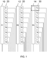
- FIG. 1 A plurality of sensing electrodes, a plurality of driving electrodes, a plurality of first connecting lines and a plurality of second connecting lines are included in the same conductive layer.
- the plurality of sensing electrodes 10, 12 and 14 are connected to respective sensing electrode signal input terminals via the first connecting lines R1, R2 and R3, respectively.
- each column of driving electrodes includes a plurality of driving electrodes 20.
- each column of driving electrodes includes eight driving electrodes 20, each of which is connected to a respective driving signal input terminal via a respective one of second connecting lines T1, T2, T3 ... T8.
- Each driving electrode and a portion of a corresponding sensing electrode constitute a capacitor 30, as shown by the dashed box in FIG. 1 .
- touch occurs in a region corresponding to the capacitor 30, the capacitance would be changed, and then a touch control signal is detected within the region.
- the number of detection points depends on the number of driving electrodes in each column of driving electrodes.
- a touch input device comprising at least one first electrode structural unit formed on a first surface of a substrate, the first electrode structural unit comprising a first column of driving electrodes comprising at least one first driving electrode; a sensing electrode extending in a column direction; and a second column of driving electrodes comprising at least one first driving electrode.
- the first column of driving electrodes, the sensing electrode and the second column of driving electrodes are arranged successively in a row direction.
- Each of the first driving electrodes is connected to a different driving signal lead, and the sensing electrode is connected to a sensing signal lead.
- Each of the first driving electrodes and a corresponding portion of the sensing electrode form a capacitor.
- a touch input device comprising at least one third electrode structural unit formed on a first surface of a substrate, the third electrode structural unit comprising a third column of driving electrodes comprising at least one third driving electrode; a column of sensing electrodes comprising at least two groups of sensing electrodes, each group comprising at least one sensing electrode; and a fourth column of driving electrodes comprising at least one third driving electrode.
- the third column of driving electrodes, the one column of sensing electrodes and the fourth column of driving electrodes are arranged successively in a row direction, each of the third driving electrodes is connected to a different driving signal lead, and the same group of sensing electrodes in the at least two groups of sensing electrodes is connected to the same sensing signal lead while different groups of sensing electrodes are connected to different sensing signal leads.
- a portion of each of the column of sensing electrodes and a portion of a corresponding one of the third column of driving electrodes form a capacitor
- another portion of each of the column of sensing electrodes and a portion of a corresponding one of the fourth column of driving electrodes form a capacitor
- the at least two groups of sensing electrodes are such arranged in a column direction that each of the third driving electrodes forms a capacitor with a portion of only one sensing electrode in each group of the at least two groups of sensing electrodes.
- a touch display device which comprises the touch input device according to the first aspect or the second aspect of the present disclosure.
- the inventive concept of the present disclosure lies in providing an improved touch input device by 1) divisionally using the sensing electrode in the horizontal direction; and 2) further divisionally using the driving electrode in the column direction.
- One sensing electrode which is divisionally used in the row direction can be further split into two adjacent sub-sensing electrodes in the row direction.
- FIG. 2 schematically illustrates a touch input device 100 according to an embodiment of the present disclosure.
- the touch input device 100 comprises at least one electrode structural unit 110 formed in a single layer on a substrate 101.
- the electrode structural unit 110 comprises a first column of driving electrodes on the left side, a second column of driving electrodes on the right side and a sensing electrode between the first column of driving electrodes and the second column of driving electrodes.
- the first column of driving electrodes, the sensing electrode and the second column of driving electrodes are arranged successively in a row direction.
- the first column of driving electrodes and the second column of driving electrodes each comprise at least one first driving electrode 112, each of which is connected to a respective different driving signal lead T1, T2, T3 ... T8.
- the sensing electrode is connected to a sensing signal lead.
- the sensing electrode is divisionally used in a horizontal direction.
- Each of the first driving electrodes 112 forms a capacitor with a corresponding portion of the sensing electrode.
- the first driving electrode 112 and the corresponding portion of the sensing electrode which form the capacitor are adjacent in the row direction.
- the first driving electrode 112 on the left side, the first driving electrode 112 on the right side, and the portions of the sensing electrode therebetween form two capacitors, one of which is formed by the first driving electrode 112 on the left side and the left adjacent portion of the sensing electrode, and the other of which is formed by the first driving electrode 112 on the right side and the right adjacent portion of the sensing electrode.
- respective capacitors formed by the sensing electrode and the driving electrodes have substantially equal capacitance to create uniformly distributed touch sensitivity. Due to the manufacture precision, the capacitance of respective capacitors may be different within a certain error range. By way of example, and not limitation, the error may be 5% or other values. As shown in FIG. 2 , the capacitance of the two capacitors marked by the dashed boxes may be substantially equal.
- the corresponding portions of the sensing electrode that form capacitors with respective first driving electrodes 112 in the first column of driving electrodes and the second column of driving electrodes may have substantially equal areas, and the first column of driving electrodes and the second column of driving electrodes may be symmetrical with respect to the sensing electrode column.
- a segment of the sensing electrode is divided by the bold dashed boxes into left and right portions that have substantially equal areas, and the area of the left (right) portion is also substantially equal to the area of the left (right) portion of a sensing electrode segment corresponding to another first driving electrode 112.
- the touch input device 100 in the touch input device 100 as shown in FIG. 2 , the length occupied in the column direction by the electrodes needed for forming sixteen capacitors (detection points) is half the length occupied by those in the prior art touch input device as shown in FIG. 1 . Meanwhile, the length occupied in the row direction is just increased slightly. Therefore, the touch input device 100 according to the embodiment can improve the touch control precision, with the same area occupied by electrodes.
- a sensing electrode can also be regarded as a plurality of discrete sub-sensing electrodes arranged in the column direction, which are electrically connected to the same sensing signal and consequently are equivalent to "one" sensing electrode in terms of function.
- At least one electrode structural unit 110 is arranged successively in the row direction to form a touch electrode array of the touch input device 100.
- the driving electrodes located at corresponding positions in respective electrode structural units 110 are connected to the same driving signal.
- the driving signals are provided by a driving module via the driving signal leads T1, T2, T3 ... T8.
- the sensing electrodes in respective electrode structural units 110 are connected to respective different sensing signals.
- the sensing signals are provided by a sensing module via the sensing signal leads R1, R2... corresponding to respective electrode structural units 110.
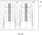
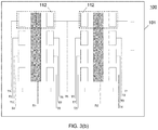
- FIGS. 3(a) to 3(c) schematically illustrate variations of the touch input device 100 according to an embodiment of the present disclosure.
- the touch input device 100 comprises at least one electrode structural unit 110 and at least one electrode structural unit 120 that are formed in a single layer on a substrate 101.
- the electrode structural unit 120 is identical with the electrode structural unit 110, except that in the electrode structural unit 120 the driving signal leads to which the first column of driving electrodes is connected and the ones to which the second column of driving electrodes is connected, are interchanged.
- the driving electrodes of the left column are connected to the driving signal leads T1, T2, T3 and T4, respectively
- the driving electrodes of the right column are connected to the driving signal leads T5, T6, T6 and T8, respectively.
- the driving electrodes of the left column are connected to the driving signal leads T5, T6, T7 and T8, respectively, and the driving electrodes of the right column are connected to the driving signal leads T1, T2, T3 and T4, respectively.
- at least one electrode structural unit 110 and at least one electrode structural unit 120 are arranged alternately in the row direction to form an electrode array.
- the driving electrodes located at corresponding positions in respective electrode structural units 110 are connected to the same driving signal
- the driving electrodes located at corresponding positions in respective electrode structural units 120 are connected to the same driving signal
- the sensing electrodes in respective electrode structural units 110 and respective electrode structural units 120 are connected to respective different sensing signals.
- one driving signal lead can be reduced between adjacent electrode structural units 110 and 120.
- each pair of adjacent first driving electrodes 112 in the row direction is merged into one complete second driving electrode 114.
- four driving signal leads can be reduced between adjacent electrode structural units 110 and 120.
- the area of the second driving electrode 114 may be two times larger than that of the first driving electrode 112, such that the capacitors formed between the sensing electrodes and the driving electrodes have substantially equal capacitance in the entire electrode array formed by the at least one electrode structural unit 110 and the at least one electrode structural unit 120, thereby creating substantially uniformly distributed touch sensitivity.
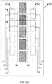
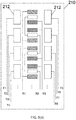
- FIG. 4 schematically illustrates a touch input device 200 according to another embodiment of the present disclosure.
- the touch input device 200 comprises at least one electrode structural unit 210 in a single layer on a substrate 201.
- the electrode structural unit 210 comprises a third column of driving electrodes on the left side, a fourth column of driving electrodes on the right side and a column of sensing electrodes between the third column of driving electrodes and the fourth column of driving electrodes.
- the third column of driving electrodes, the column of sensing electrodes and the fourth column of driving electrodes are arranged successively in a row direction.
- the third column of driving electrodes and the fourth column of driving electrodes each comprise at least one third driving electrode 212, each of which is connected to a respective different driving signal lead T1, T2, T3 ... T8.
- the column of sensing electrodes comprises at least two groups of sensing electrodes, as marked by different shadow lines in FIG. 4 , wherein sensing electrodes of the same group are connected to the same sensing signal lead, while sensing electrodes of different groups are connected to different sensing signal leads. For example, in FIG. 4 , two groups of sensing electrodes marked with different shadow lines are connected to sensing signal leads R1 and R2, respectively.
- each sensing electrode and a portion of a corresponding third driving electrode 212 in the first column of driving electrodes form a capacitor
- another portion of each sensing electrode and a portion of a corresponding third driving electrode 212 in the second column of driving electrodes form a capacitor.
- the portion of the sensing electrode and the portion of the third driving electrode 212 which form the capacitor are adjacent in the row direction. For example, as shown by the bold dashed boxes in FIG.
- the third driving electrode 212 on the left side, the third driving electrode 212 on the right side and the two sensing electrodes therebetween form four capacitors, wherein the upper portion of the third driving electrode 212 on the left side and the left portion of the upper sensing electrode form one capacitor, the upper portion of the third driving electrode 212 on the right side and the right portion of the upper sensing electrode form one capacitor, the lower portion of the third driving electrode 212 on the left side and the left portion of the lower sensing electrode form one capacitor, and the lower portion of the third driving electrode 212 on the right side and the right portion of the lower sensing electrode form one capacitor.
- respective capacitors formed by the sensing electrodes and the driving electrodes have substantially equal capacitance to create uniformly distributed touch sensitivity.
- the capacitance of respective capacitors may be different within a certain error range.
- the error may be 5% or other values.
- the capacitance of the four capacitors marked by the bold dashed boxes may be substantially equal.
- the areas of the portions of each sensing electrode that form capacitors with the third driving electrodes 212 in the first column of driving electrodes or the second column of driving electrodes may be substantially equal, and the driving electrodes of the first column and the driving electrodes of the second column may be symmetrical with respect to the column of sensing electrodes.
- the upper and lower sensing electrodes are divided by the bold dashed boxes into two portions, respectively, the resultant four portions have substantially equal areas, and the areas are also substantially equal to the areas of the portions of the sensing electrodes which correspond to other third driving electrodes 212.
- each third driving electrode 212 forms a capacitor with a portion of only one sensing electrode in each group in the at least two groups of sensing electrodes.
- each third driving electrode 212 "traverses" the sensing electrodes of each group once and only once (further discussed below).
- the at least one electrode structural unit 210 is arranged successively in the row direction to form a touch electrode array of the touch input device 200.
- the driving electrodes located at corresponding positions in respective electrode structural units 210 are connected to the same driving signal.
- the driving signals are provided by a driving module via the driving signal leads T1, T2, T3 ... T8.
- the sensing electrodes in respective electrode structural units 210 are connected to different sensing signals.
- the sensing signals are provided by a sensing module via the sensing signal leads R1, R2, R3, R4, R5, R6... corresponding to respective electrode structural units 210.
- FIGS. 5(a) to 5(f) schematically illustrate variations of the electrode structural unit 210 in the touch input device 200 as shown in FIG. 4 .
- FIG. 5(a) illustrates a sensing electrode arrangement different from that in FIG. 4 .
- the respective sensing electrodes are arranged from top to down in the order of R1, R2, R2, R1, R1, R2, R2, R1..., and so on (in the description below, the symbols "Rx"s of the sensing signal leads to which the respective sensing electrodes are connected will be used to represent different sensing electrode groups).
- the column of sensing electrodes may comprise two types of sub-columns that are arranged alternately in the column direction, wherein each sub-column consists of one sensing electrode in each sensing electrode group, the sensing electrodes in the first type of sub-column are arranged in a first order, and the sensing electrodes in the second type of sub-column are arranged in a second order reverse to the first order.
- the respective sensing electrodes are arranged from top to down in the order of R1, R2, R2, R1, R1, R2..., and so on.
- each third driving electrode 212 "traverses" the sensing electrodes R1 and R2 once. Further, the capacitors formed by the sensing electrodes and the corresponding third driving electrodes 212 may have substantially equal capacitance.
- FIG. 5(b) illustrates a variation of the sensing electrode arrangement shown in FIG. 5(a) , in which two sensing electrodes that are adjacent in the column direction and belong to the same group are merged into one complete electrode.
- FIG. 5(b) illustrates a variation of the sensing electrode arrangement shown in FIG. 5(a) , in which two sensing electrodes that are adjacent in the column direction and belong to the same group are merged into one complete electrode.
- the third driving electrode 212 on the left side, the third driving electrode 212 on the right side and two sensing electrodes u, d therebetween form four capacitors, wherein the upper portion of the third driving electrode 212 on the left side and the lower left portion of the sensing electrode u form one capacitor, the upper portion of the third driving electrode 212 on the right side and the lower right portion of the sensing electrode u form one capacitor, the lower portion of the third driving electrode 212 on the left side and the upper left portion of the sensing electrode d form one capacitor, and the lower portion of the third driving electrode 212 on the right side and the upper right portion of the sensing electrode d form one capacitor.
- each third driving electrode 212 "traverses" the sensing electrodes R1 and R2 once. Further, the capacitors formed by the sensing electrodes and the corresponding third driving electrodes 212 may have substantially equal capacitance.
- FIG. 5(c) schematically illustrates an electrode structural unit 210 having three groups of sensing electrodes in the touch input device 200 according to an embodiment of the present disclosure, in which the respective sensing electrodes are arranged from top to down in the order of R1, R2, R3, R1, R2, R3..., and so on.
- each third driving electrode 212 "traverses" the sensing electrodes R1, R2 and R3 once.
- the capacitors formed by the sensing electrodes and the corresponding third driving electrodes 212 may have substantially equal capacitance.
- sensing electrode arrangement shown in FIG. 5(c) , since there are three groups of sensing signal leads R1, R2 and R3, while the sensing signal leads can only be led out from two sides of the sensing electrode, in order to avoid intersection between the sensing signal leads, wiring must be done between adjacent sensing electrodes along the row direction (e.g. wiring of the sensing electrode R2). This may be disadvantageous because the spacing between the sensing electrodes is very small, and such a design would require high processing precision and may result in crosstalk between scanning signals.
- FIG. 5(d) illustrates a variation of the sensing electrode arrangement shown in FIG. 5(c) , in which the respective sensing electrodes are arranged from top to down in the order of R1, R2, R3, R3, R2, R1..., and so on.
- the column of sensing electrodes may comprise two types of sub-columns arranged alternately in the column direction, wherein the first type of sub-column is R1-R2-R3, and the second type of sub-column is R3, R2, R1.
- each third driving electrode 212 "traverses" the sensing electrodes R1, R2 and R3 once. Use of such an arrangement avoids wiring between adjacent sensing electrodes along the row direction, and hence the above possible deficiency.
- the capacitors formed by the sensing electrodes and the corresponding third driving electrodes 212 may have substantially equal capacitance.
- FIG. 5(e) further adds one group of sensing electrodes on the basis of the sensing electrodes in FIG. 5(d) .
- the respective sensing electrodes are arranged from top to down in the order of R1, R2, R3, R4, R4, R3, R2, R1..., and so on.
- the first type of sub-column is R1-R2-R3-R4
- the second type of sub-column is R4-R3-R2-R1.
- each third driving electrode 212 "traverses" the sensing electrodes R1, R2, R3 and R4 once. Use of such an arrangement avoids wiring between adjacent sensing electrodes along the row direction, and hence the above possible deficiency.
- the capacitors formed by the sensing electrodes and the corresponding third driving electrodes 212 may have substantially equal capacitance.
- FIG. 5(f) illustrates a variation of the sensing electrode arrangement shown in FIG. 5(d) , in which two sensing electrodes that are adjacent in the column direction and belong to the same group are merged into one complete electrode.
- the third driving electrode 212 on the left side, the third driving electrode 212 on the right side and three sensing electrodes therebetween form six capacitors.
- each third driving electrode 212 "traverses" the sensing electrodes R1, R2 and R3 once.
- the capacitors formed by the sensing electrodes and the corresponding third driving electrodes 212 may have substantially equal capacitance.
- the at least one electrode structural unit 210 is arranged successively in the row direction to form an electrode array on the substrate 201.
- the electrode structural unit 210 in the touch input device 200 may be any one of the electrode structural units 210 shown in FIGS. 5(a) to 5(f) , and the electrode structural units 210 shown in FIGS. 5(a) to 5(f) are only illustrative rather than restrictive. For example, it is also possible to use five or even more groups of sensing electrodes in the electrode structural unit 210.
- FIG. 6 schematically illustrates a variation of the touch input device 200 shown in FIG. 4 .
- the touch input device 200 comprises at least one electrode structural unit 210 and at least one electrode structural unit 220 in a single layer on a substrate 201.
- the electrode structural unit 220 is identical with the electrode structural unit 210, except that in the electrode structural unit 220 the driving signal leads to which the first column of driving electrodes is connected and the ones to which the second column of driving electrodes is connected are interchanged.
- the driving electrodes of the left column are connected to the driving signal leads T1, T2, T3 and T4, respectively
- the driving electrodes of the right column are connected to the driving signal leads T5, T6, T6 and T8, respectively.
- the driving electrodes of the left column are connected to the driving signal leads T5, T6, T7 and T8, respectively, and the driving electrodes of the right column are connected to the driving signal leads T1, T2, T3 and T4, respectively.
- the at least one electrode structural unit 210 and the at least one electrode structural unit 220 are arranged alternately in the row direction to form an electrode array.
- the driving electrodes located at corresponding positions in respective electrode structural units 210 are connected to the same driving signal
- the driving electrodes located at corresponding positions in respective electrode structural units 220 are connected to the same driving signal
- the sensing electrodes in respective electrode structural units 210 and respective electrode structural units 220 are connected to respective different sensing signals.
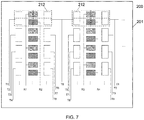
- FIG. 7 schematically illustrates a variation of the touch input device 200 shown in FIG. 6 , in which the last pair of first driving electrodes 112 between adjacent electrode structural units 210 and 220 in a direction opposite to a direction in which the diving signal leads T1, T2, T3 ... T8 extend shares the same driving signal lead.
- one driving signal lead can be reduced between adjacent electrode structural units 210 and 220.
- FIG. 8 schematically illustrates another variation of the touch input device 200 shown in FIG. 6 , in which each pair of adjacent first driving electrodes 212 between adjacent electrode structural units 210 and 220 in the row direction is merged into one complete fourth driving electrode 214.
- the fourth driving electrode 214 may have an area two times larger than that of the third driving electrode 212, such that the capacitors formed between the sensing electrodes and the driving electrodes have substantially equal capacitance in the entire electrode array formed by the at least one electrode structural unit 210 and the at least one electrode structural unit 220, thereby creating substantially uniformly distributed touch sensitivity.
- the sensing electrodes in the electrode structural units 210 and 220 may be arranged in any of the sensing electrode arrangements shown in FIGS. 5(a) to 5(f) , and the sensing electrode arrangements shown in FIGS. 5(a) to 5(f) are only illustrative rather than restrictive.
- FIG. 9 schematically illustrates another variation of the touch input device 200 shown in FIG. 4 .
- each sensing electrode comprises a first sub-sensing electrode and a second sub-sensing electrode which are adjacent in the row direction.
- one sensing electrode is split into two adjacent sub-sensing electrodes in the row direction.
- the first sub-sensing electrode corresponds to the portion of the sensing electrode which forms a capacitor with a portion of a corresponding third driving electrode in the third column of driving electrodes
- the second sub-sensing electrode corresponds to the portion of the sensing electrode which forms a capacitor with a portion of a corresponding third driving electrode in the fourth column of driving electrodes.
- the first sub-sensing electrode and a portion of the corresponding third driving electrode 212 in the third column of driving electrodes form a capacitor
- the second sub-sensing electrode and a portion of the corresponding third driving electrode 212 in the fourth column of driving electrodes form a capacitor.
- the first sub-sensing electrode or second sub-sensing electrode and the portion of the third driving electrode 212 which form the capacitor are adjacent in the row direction. For example, as shown by the bold dashed boxes in FIG.
- the third driving electrode 212 on the left side, the third driving electrode 212 on the right side and four sub-sensing electrodes therebetween form four capacitors, wherein the upper portion of the third driving electrode 212 on the left side and the upper first sub-sensing electrode form one capacitor, the upper portion of the third driving electrode 212 on the right side and the upper second sub-sensing electrode form one capacitor, the lower portion of the third driving electrode 212 on the left side and the lower first sub-sensing electrode form one capacitor, and the lower portion of the third driving electrode 212 on the right side and the lower second sub-sensing electrode form one capacitor.
- each third driving electrode 212 "traverses" the (sub) sensing electrodes R1 and R2 once.
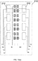
- FIGS. 10(a) to 10(g) schematically illustrate variations of the electrode structural unit 210 in the touch input device 200 shown in FIG. 9 .
- the electrode arrangement in FIG. 10(a) is the same as the electrode arrangement of the electrode structural unit 210 in FIG. 9 , except for the wiring of the sensing signal leads of the sensing electrodes. As compared to the former, one sensing signal lead is reduced in each electrode structural unit 210.
- FIG. 10(b) illustrates a different sensing electrode arrangement, in which respective sensing electrodes are arranged from top to down in the order of R1, R2, R2, R1, R1, R2, R2, R1..., and so on.
- the column of sensing electrodes may comprise two types of sub-columns arranged alternately in the column direction, wherein each sub-column consists of one sensing electrode in each sensing electrode group, the sensing electrodes in the first type of sub-columns are arranged in a first order, and the sensing electrodes in the second type of sub-columns are arranged in a second order reverse to the first order.
- each sensing electrode comprises a first sub-sensing electrode and a second sub-sensing electrode which are adjacent in the row direction
- the column of sensing electrodes actually comprises one column of first sub-sensing electrodes and one column of second sub-sensing electrodes.
- each third driving electrode 212 "traverses" the (sub) sensing electrodes R1 and R2 once.
- FIG. 10(c) illustrates a variation of the sensing electrode arrangement shown in FIG. 10(b) , in which two first sub-sensing electrodes or second sub-sensing electrodes that are adjacent in the column direction and belong to the same group are merged into one complete electrode.
- each third driving electrode 212 "traverses" the (sub) sensing electrodes R1 and R2 once.
- FIG. 10(d) schematically illustrates an electrode structural unit 210 having three groups of sensing electrodes in the touch input device 200 according to an embodiment of the present disclosure.
- the respective sensing electrodes are arranged from top to down in the order of R1, R2, R3, R1, R2, R3..., and so on.
- each third driving electrode 212 "traverses" the (sub) sensing electrodes R1, R2 and R3 once.
- FIG. 10(e) illustrates a variation of the sensing electrode arrangement manner shown in FIG. 10(d) , in which the respective sensing electrodes are arranged from top to down in the order of R1, R2, R3, R3, R2, R1..., and so on.
- the column of sensing electrodes may comprise two types of sub-columns arranged alternately in the column direction, wherein the first type of sub-column is R1-R2-R3, and the second type of sub-column is R3-R2-R1.
- each third driving electrode 212 "traverses" the (sub) sensing electrodes R1, R2 and R3 once. Use of such an arrangement avoids wiring between adjacent sensing electrodes along the row direction.
- FIG. 10(f) further adds one group of sensing electrodes on the basis of the sensing electrodes in FIG. 10(e) .
- the respective sensing electrodes are arranged from top to down in the order of R1, R2, R3, R4, R4, R3, R2, R1..., and so on.
- the first type of sub-column is R1-R2-R3-R4
- the second type of sub-column is R4-R3-R2-R1.
- each third driving electrode 212 "traverses" the (sub) sensing electrodes R1, R2, R3 and R4 once. Use of such an arrangement avoids wiring between adjacent sensing electrodes along the row direction.
- FIG. 10(g) illustrates a variation of the sensing electrode arrangement manner shown in FIG. 10(e) , in which two first sub-sensing electrodes or second sub-sensing electrodes that are adjacent in the column direction and belong to the same group are merged into one complete electrode.
- the third driving electrode 212 on the left side, the third driving electrode 212 on the right side and six sub-sensing electrodes therebetween form six capacitors.
- each third driving electrode 212 "traverses" the (sub) sensing electrodes R1, R2 and R3 once.
- the at least one electrode structural unit 210 is arranged successively in the row direction to form an electrode array on the substrate 201.
- the electrode structural unit 210 in the touch input device 200 may be any one of the electrode structural units 210 shown in FIGS. 10(a) to 10(g) , and the electrode structural units 210 shown in FIGS. 10(a) to 10(g) are only illustrative rather than restrictive. For example, it is also possible to use five or even more groups of sensing electrodes in the electrode structural unit 210.
- FIG. 11 schematically illustrates a variation of the touch input device 200 shown in FIG. 9 .
- the touch input device 200 comprises at least one electrode structural unit 210 and at least one electrode structural unit 220 in a single layer on a substrate 201.
- the electrode structural unit 220 is identical with the electrode structural unit 210, except that in the electrode structural unit 220 the driving signal leads to which the third column of driving electrodes is connected and the ones to which the fourth column of driving electrodes is connected are interchanged.
- the at least one electrode structural unit 210 and the at least one electrode structural unit 220 are arranged alternately in the row direction to form an electrode array.
- the driving electrodes located at corresponding positions in respective electrode structural units 210 are connected to the same driving signal
- the driving electrodes located at corresponding positions in respective electrode structural units 220 are connected to the same driving signal
- the sensing electrodes in respective electrode structural units 210 and respective electrode structural units 220 are connected to respective different sensing signals.
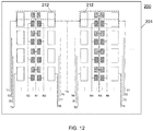
- FIG. 12 schematically illustrates a variation of the touch input device 200 shown in FIG. 11 , in which the last pair of third driving electrodes 212 between adjacent electrode structural units 210 and 220 in a direction opposite to a direction in which the diving signal leads T1, T2, T3 ... T8 extend shares the same driving signal lead.
- one driving signal lead can be reduced between adjacent electrode structural units 210 and 220.
- FIG. 13 schematically illustrates another variation of the touch input device 200 shown in FIG. 11 , in which each pair of adjacent third driving electrodes 212 between adjacent electrode structural units 210 and 220 in the row direction is merged into one complete fourth driving electrode 214.
- the fourth driving electrode 214 may have an area two times larger than that of the third driving electrode 212, such that the capacitors formed between the sensing electrodes and the driving electrodes have substantially equal capacitance in the entire electrode array formed by the at least one electrode structural unit 210 and the at least one electrode structural unit 220, thereby creating substantially uniformly distributed touch sensitivity.
- the sensing electrodes in the electrode structural units 210 and 220 may be arranged in any of the sensing electrode arrangements shown in FIGS. 10(a) to 10(g) , and the sensing electrode arrangements shown in FIGS. 10(a) to 10(g) are only illustrative rather than restrictive.
- a touch display device which comprises any of the touch input devices described in the above embodiments.
- the touch display device comprises other components such as a display screen, which is well known in the art and will not be discussed here in detail.
Landscapes
- Engineering & Computer Science (AREA)
- General Engineering & Computer Science (AREA)
- Theoretical Computer Science (AREA)
- Human Computer Interaction (AREA)
- Physics & Mathematics (AREA)
- General Physics & Mathematics (AREA)
- Computer Networks & Wireless Communication (AREA)
- Position Input By Displaying (AREA)
Abstract
Description
- The present disclosure relates to the field of touch input technologies, and more particularly to a touch input device and a touch display device.
- A touch panel is an input apparatus through which one moves a cursor or inputs an instruction by means of sliding or clicking operations with a touch object such as a finger. For a capacitive touch panel, capacitance would be changed when a user's finger gets close to the touch panel. The change in the capacitance is detected by the touch panel itself and converted into coordinates, such that movements of the finger are derived and converted into corresponding control commands.
- Traditional capacitive touch sensors typically have a two-layered structure (i.e., a layer of driving electrodes Tx and a layer of sensing electrodes Rx), resulting in high cost. Recently, a solution of a touch screen using monolayer sensors has been proposed. The typical structure of the monolayer sensors is as shown in
FIG. 1 . A plurality of sensing electrodes, a plurality of driving electrodes, a plurality of first connecting lines and a plurality of second connecting lines are included in the same conductive layer. The plurality ofsensing electrodes adjacent sensing electrodes electrodes 20. In this example, each column of driving electrodes includes eightdriving electrodes 20, each of which is connected to a respective driving signal input terminal via a respective one of second connecting lines T1, T2, T3 ... T8. Each driving electrode and a portion of a corresponding sensing electrode constitute acapacitor 30, as shown by the dashed box inFIG. 1 . When touch occurs in a region corresponding to thecapacitor 30, the capacitance would be changed, and then a touch control signal is detected within the region. With each capacitor being a detection point, the number of detection points depends on the number of driving electrodes in each column of driving electrodes. - With the increased size of the display panel and the improved touch control resolution, it is required to not only increase the number of sensing electrodes and driving electrodes in the entire panel region, but also increase the number of sensing electrodes and driving electrodes in a unit area. However, further improvement of the touch control resolution is limited in the existing design. For example, as the number of electrodes increases, more second connecting lines are needed to transmit driving signals thereto, which causes more difficulties in wiring and design of driver chips and results in an oversized flexible print circuit (FPC) that is to be bonded.
- Accordingly, there is a need for an improved touch input device and a touch display device using the same.
- It is an object of the present disclosure to provide an improved touch input device and a touch display device using the same.
- In a first aspect of the present disclosure, a touch input device is provided comprising at least one first electrode structural unit formed on a first surface of a substrate, the first electrode structural unit comprising a first column of driving electrodes comprising at least one first driving electrode; a sensing electrode extending in a column direction; and a second column of driving electrodes comprising at least one first driving electrode. The first column of driving electrodes, the sensing electrode and the second column of driving electrodes are arranged successively in a row direction. Each of the first driving electrodes is connected to a different driving signal lead, and the sensing electrode is connected to a sensing signal lead. Each of the first driving electrodes and a corresponding portion of the sensing electrode form a capacitor. By divisionally using the sensing electrodes in the row direction, improved touch control resolution is achieved with the same area occupied by electrodes.
- According to a second aspect of the present disclosure, a touch input device is provided comprising at least one third electrode structural unit formed on a first surface of a substrate, the third electrode structural unit comprising a third column of driving electrodes comprising at least one third driving electrode; a column of sensing electrodes comprising at least two groups of sensing electrodes, each group comprising at least one sensing electrode; and a fourth column of driving electrodes comprising at least one third driving electrode. The third column of driving electrodes, the one column of sensing electrodes and the fourth column of driving electrodes are arranged successively in a row direction, each of the third driving electrodes is connected to a different driving signal lead, and the same group of sensing electrodes in the at least two groups of sensing electrodes is connected to the same sensing signal lead while different groups of sensing electrodes are connected to different sensing signal leads. A portion of each of the column of sensing electrodes and a portion of a corresponding one of the third column of driving electrodes form a capacitor, another portion of each of the column of sensing electrodes and a portion of a corresponding one of the fourth column of driving electrodes form a capacitor, and the at least two groups of sensing electrodes are such arranged in a column direction that each of the third driving electrodes forms a capacitor with a portion of only one sensing electrode in each group of the at least two groups of sensing electrodes. By divisionally using the driving electrodes in the column direction, the number of driving electrode leads is reduced.
- According to a third aspect of the present disclosure, a touch display device is provided which comprises the touch input device according to the first aspect or the second aspect of the present disclosure.
- The inventive concept of the present disclosure lies in providing an improved touch input device by 1) divisionally using the sensing electrode in the horizontal direction; and 2) further divisionally using the driving electrode in the column direction. One sensing electrode which is divisionally used in the row direction can be further split into two adjacent sub-sensing electrodes in the row direction.
- These and other aspects of the present disclosure would be apparent from and elucidated with reference to the embodiments described below.
-
-
FIG. 1 schematically illustrates an electrode structure in a monolayer capacitive touch screen in the prior art; -
FIG. 2 schematically illustrates a touch input device according to an embodiment of the present disclosure; -
FIGS. 3(a) to 3(c) schematically illustrate variations of the touch input device according to an embodiment of the present disclosure; -
FIG. 4 schematically illustrates a touch input device according to another embodiment of the present disclosure; -
FIGS. 5(a) to 5(f) schematically illustrate variations of the electrode structural unit in the touch input device shown inFIG. 4 ; -
FIG. 6 schematically illustrates a variation of the touch input device shown inFIG. 4 ; -
FIG. 7 schematically illustrates a variation of the touch input device shown inFIG. 6 ; -
FIG. 8 schematically illustrates another variation of the touch input device shown inFIG. 6 ; -
FIG. 9 schematically illustrates another variation of the touch input device shown inFIG. 4 ; -
FIGS. 10(a) to 10(g) schematically illustrate variations of the electrode structural unit in the touch input device shown inFIG. 9 ; -
FIG. 11 schematically illustrates a variation of the touch input device shown inFIG. 9 ; -
FIG. 12 schematically illustrates a variation of the touch input device shown inFIG. 11 ; and -
FIG. 13 schematically illustrates another variation of the touch input device shown inFIG. 11 . - Embodiments of the present disclosure are described below in detail with reference to the drawings.
-
FIG. 2 schematically illustrates atouch input device 100 according to an embodiment of the present disclosure. Thetouch input device 100 comprises at least one electrodestructural unit 110 formed in a single layer on asubstrate 101. As shown in the figure, the electrodestructural unit 110 comprises a first column of driving electrodes on the left side, a second column of driving electrodes on the right side and a sensing electrode between the first column of driving electrodes and the second column of driving electrodes. In other words, the first column of driving electrodes, the sensing electrode and the second column of driving electrodes are arranged successively in a row direction. - In the electrode
structural unit 110, the first column of driving electrodes and the second column of driving electrodes each comprise at least onefirst driving electrode 112, each of which is connected to a respective different driving signal lead T1, T2, T3 ... T8. The sensing electrode is connected to a sensing signal lead. - As shown in
FIG. 2 , the sensing electrode is divisionally used in a horizontal direction. Each of thefirst driving electrodes 112 forms a capacitor with a corresponding portion of the sensing electrode. Thefirst driving electrode 112 and the corresponding portion of the sensing electrode which form the capacitor are adjacent in the row direction. For example, as illustrated by the bold dashed boxes inFIG. 2 , thefirst driving electrode 112 on the left side, thefirst driving electrode 112 on the right side, and the portions of the sensing electrode therebetween form two capacitors, one of which is formed by thefirst driving electrode 112 on the left side and the left adjacent portion of the sensing electrode, and the other of which is formed by thefirst driving electrode 112 on the right side and the right adjacent portion of the sensing electrode. - It is desirable that respective capacitors formed by the sensing electrode and the driving electrodes have substantially equal capacitance to create uniformly distributed touch sensitivity. Due to the manufacture precision, the capacitance of respective capacitors may be different within a certain error range. By way of example, and not limitation, the error may be 5% or other values. As shown in
FIG. 2 , the capacitance of the two capacitors marked by the dashed boxes may be substantially equal. For example, in the electrodestructural unit 110, the corresponding portions of the sensing electrode that form capacitors with respective first drivingelectrodes 112 in the first column of driving electrodes and the second column of driving electrodes may have substantially equal areas, and the first column of driving electrodes and the second column of driving electrodes may be symmetrical with respect to the sensing electrode column. For instance, as shown inFIG. 2 , a segment of the sensing electrode is divided by the bold dashed boxes into left and right portions that have substantially equal areas, and the area of the left (right) portion is also substantially equal to the area of the left (right) portion of a sensing electrode segment corresponding to anotherfirst driving electrode 112. - In this way, in the
touch input device 100 as shown inFIG. 2 , the length occupied in the column direction by the electrodes needed for forming sixteen capacitors (detection points) is half the length occupied by those in the prior art touch input device as shown inFIG. 1 . Meanwhile, the length occupied in the row direction is just increased slightly. Therefore, thetouch input device 100 according to the embodiment can improve the touch control precision, with the same area occupied by electrodes. - It is to be understood that in this embodiment, the so-called "a sensing electrode" can also be regarded as a plurality of discrete sub-sensing electrodes arranged in the column direction, which are electrically connected to the same sensing signal and consequently are equivalent to "one" sensing electrode in terms of function.
- At least one electrode
structural unit 110 is arranged successively in the row direction to form a touch electrode array of thetouch input device 100. As known to those skilled in the art, the driving electrodes located at corresponding positions in respective electrodestructural units 110 are connected to the same driving signal. In this example, the driving signals are provided by a driving module via the driving signal leads T1, T2, T3 ... T8. The sensing electrodes in respective electrodestructural units 110 are connected to respective different sensing signals. In this example, the sensing signals are provided by a sensing module via the sensing signal leads R1, R2... corresponding to respective electrodestructural units 110. -
FIGS. 3(a) to 3(c) schematically illustrate variations of thetouch input device 100 according to an embodiment of the present disclosure. - As shown in
FIG. 3(a) , thetouch input device 100 comprises at least one electrodestructural unit 110 and at least one electrodestructural unit 120 that are formed in a single layer on asubstrate 101. The electrodestructural unit 120 is identical with the electrodestructural unit 110, except that in the electrodestructural unit 120 the driving signal leads to which the first column of driving electrodes is connected and the ones to which the second column of driving electrodes is connected, are interchanged. In other words, in the electrodestructural unit 110, the driving electrodes of the left column are connected to the driving signal leads T1, T2, T3 and T4, respectively, and the driving electrodes of the right column are connected to the driving signal leads T5, T6, T6 and T8, respectively. However, in the electrodestructural unit 120, the driving electrodes of the left column are connected to the driving signal leads T5, T6, T7 and T8, respectively, and the driving electrodes of the right column are connected to the driving signal leads T1, T2, T3 and T4, respectively. In thetouch input device 100, at least one electrodestructural unit 110 and at least one electrodestructural unit 120 are arranged alternately in the row direction to form an electrode array. As known to those skilled in the art, the driving electrodes located at corresponding positions in respective electrodestructural units 110 are connected to the same driving signal, the driving electrodes located at corresponding positions in respective electrodestructural units 120 are connected to the same driving signal, and the sensing electrodes in respective electrodestructural units 110 and respective electrodestructural units 120 are connected to respective different sensing signals. - As shown in
FIG. 3(b) , between adjacent electrodestructural units first driving electrodes 112 in a direction opposite to a direction in which the driving signal leads T1, T2, T3 ... T8 extend shares the same driving signal lead. In this way, as compared with the example shown inFIG. 3(a) , one driving signal lead can be reduced between adjacent electrodestructural units - As shown in
FIG. 3(c) , between adjacent electrodestructural units first driving electrodes 112 in the row direction is merged into one completesecond driving electrode 114. In this way, as compared with the example shown inFIG. 3(a) , four driving signal leads can be reduced between adjacent electrodestructural units second driving electrode 114 may be two times larger than that of thefirst driving electrode 112, such that the capacitors formed between the sensing electrodes and the driving electrodes have substantially equal capacitance in the entire electrode array formed by the at least one electrodestructural unit 110 and the at least one electrodestructural unit 120, thereby creating substantially uniformly distributed touch sensitivity. -
FIG. 4 schematically illustrates atouch input device 200 according to another embodiment of the present disclosure. Thetouch input device 200 comprises at least one electrodestructural unit 210 in a single layer on asubstrate 201. As shown in the figure, the electrodestructural unit 210 comprises a third column of driving electrodes on the left side, a fourth column of driving electrodes on the right side and a column of sensing electrodes between the third column of driving electrodes and the fourth column of driving electrodes. In other words, the third column of driving electrodes, the column of sensing electrodes and the fourth column of driving electrodes are arranged successively in a row direction. - In the electrode
structural unit 210, the third column of driving electrodes and the fourth column of driving electrodes each comprise at least onethird driving electrode 212, each of which is connected to a respective different driving signal lead T1, T2, T3 ... T8. The column of sensing electrodes comprises at least two groups of sensing electrodes, as marked by different shadow lines inFIG. 4 , wherein sensing electrodes of the same group are connected to the same sensing signal lead, while sensing electrodes of different groups are connected to different sensing signal leads. For example, inFIG. 4 , two groups of sensing electrodes marked with different shadow lines are connected to sensing signal leads R1 and R2, respectively. - A portion of each sensing electrode and a portion of a corresponding
third driving electrode 212 in the first column of driving electrodes form a capacitor, and another portion of each sensing electrode and a portion of a correspondingthird driving electrode 212 in the second column of driving electrodes form a capacitor. The portion of the sensing electrode and the portion of thethird driving electrode 212 which form the capacitor are adjacent in the row direction. For example, as shown by the bold dashed boxes inFIG. 4 , thethird driving electrode 212 on the left side, thethird driving electrode 212 on the right side and the two sensing electrodes therebetween form four capacitors, wherein the upper portion of thethird driving electrode 212 on the left side and the left portion of the upper sensing electrode form one capacitor, the upper portion of thethird driving electrode 212 on the right side and the right portion of the upper sensing electrode form one capacitor, the lower portion of thethird driving electrode 212 on the left side and the left portion of the lower sensing electrode form one capacitor, and the lower portion of thethird driving electrode 212 on the right side and the right portion of the lower sensing electrode form one capacitor. - It is desirable that respective capacitors formed by the sensing electrodes and the driving electrodes have substantially equal capacitance to create uniformly distributed touch sensitivity. As stated above, due to the manufacture precision, the capacitance of respective capacitors may be different within a certain error range. By way of example, and not limitation, the error may be 5% or other values. As shown in
FIG. 4 , the capacitance of the four capacitors marked by the bold dashed boxes may be substantially equal. For example, in the electrodestructural unit 210, the areas of the portions of each sensing electrode that form capacitors with thethird driving electrodes 212 in the first column of driving electrodes or the second column of driving electrodes may be substantially equal, and the driving electrodes of the first column and the driving electrodes of the second column may be symmetrical with respect to the column of sensing electrodes. For instance, as shown inFIG. 4 , the upper and lower sensing electrodes are divided by the bold dashed boxes into two portions, respectively, the resultant four portions have substantially equal areas, and the areas are also substantially equal to the areas of the portions of the sensing electrodes which correspond to otherthird driving electrodes 212. - In this way, in the
touch input device 200 as shown inFIG. 4 , only two sensing signal leads R1 and R2, and eight driving signal leads T1, T2, T3 ... T8, are needed to form sixteen capacitors (detection points). However, in the prior art as shown inFIG. 1 , two sensing signal leads and sixteen driving signal leads are needed. Therefore, as compared to the prior art, the number of driving signal leads is reduced in this embodiment. - In the electrode arrangement shown in
FIG. 4 , two groups of sensing electrodes are arranged alternately in the column direction. It is to be understood that the electrode arrangement shown inFIG. 4 is just exemplary. In practice, in this embodiment, at least two groups of sensing electrodes can be such arranged in the column direction that each of thethird driving electrodes 212 forms a capacitor with a portion of only one sensing electrode in each group in the at least two groups of sensing electrodes. In other words, analogous to the concept of "traversing" in the path search, eachthird driving electrode 212 "traverses" the sensing electrodes of each group once and only once (further discussed below). - The at least one electrode
structural unit 210 is arranged successively in the row direction to form a touch electrode array of thetouch input device 200. As known to those skilled in the art, the driving electrodes located at corresponding positions in respective electrodestructural units 210 are connected to the same driving signal. In this example, the driving signals are provided by a driving module via the driving signal leads T1, T2, T3 ... T8. The sensing electrodes in respective electrodestructural units 210 are connected to different sensing signals. In this example, the sensing signals are provided by a sensing module via the sensing signal leads R1, R2, R3, R4, R5, R6... corresponding to respective electrodestructural units 210. -
FIGS. 5(a) to 5(f) schematically illustrate variations of the electrodestructural unit 210 in thetouch input device 200 as shown inFIG. 4 . -
FIG. 5(a) illustrates a sensing electrode arrangement different from that inFIG. 4 . The respective sensing electrodes are arranged from top to down in the order of R1, R2, R2, R1, R1, R2, R2, R1..., and so on (in the description below, the symbols "Rx"s of the sensing signal leads to which the respective sensing electrodes are connected will be used to represent different sensing electrode groups). In such an arrangement, the column of sensing electrodes may comprise two types of sub-columns that are arranged alternately in the column direction, wherein each sub-column consists of one sensing electrode in each sensing electrode group, the sensing electrodes in the first type of sub-column are arranged in a first order, and the sensing electrodes in the second type of sub-column are arranged in a second order reverse to the first order. For example, as shown inFIG. 5(a) , the respective sensing electrodes are arranged from top to down in the order of R1, R2, R2, R1, R1, R2..., and so on. In this example, the first type of sub-column is R1-R2, and the second type of sub-column is R2-R1. As stated above, eachthird driving electrode 212 "traverses" the sensing electrodes R1 and R2 once. Further, the capacitors formed by the sensing electrodes and the corresponding third drivingelectrodes 212 may have substantially equal capacitance. - Alternatively,
FIG. 5(b) illustrates a variation of the sensing electrode arrangement shown inFIG. 5(a) , in which two sensing electrodes that are adjacent in the column direction and belong to the same group are merged into one complete electrode. In this case, as shown by the bold dashedbox 1a inFIG. 5(b) , thethird driving electrode 212 on the left side, thethird driving electrode 212 on the right side and two sensing electrodes u, d therebetween form four capacitors, wherein the upper portion of thethird driving electrode 212 on the left side and the lower left portion of the sensing electrode u form one capacitor, the upper portion of thethird driving electrode 212 on the right side and the lower right portion of the sensing electrode u form one capacitor, the lower portion of thethird driving electrode 212 on the left side and the upper left portion of the sensing electrode d form one capacitor, and the lower portion of thethird driving electrode 212 on the right side and the upper right portion of the sensing electrode d form one capacitor. Particularly, as shown by the bold dashedbox 1b, for the sensing electrode d, its lower left portion further forms one capacitor with the upper portion of the driving electrode on its left side, and its lower right portion further forms one capacitor with the upper portion of the driving electrode on its right side. As stated above, eachthird driving electrode 212 "traverses" the sensing electrodes R1 and R2 once. Further, the capacitors formed by the sensing electrodes and the corresponding third drivingelectrodes 212 may have substantially equal capacitance. -
FIG. 5(c) schematically illustrates an electrodestructural unit 210 having three groups of sensing electrodes in thetouch input device 200 according to an embodiment of the present disclosure, in which the respective sensing electrodes are arranged from top to down in the order of R1, R2, R3, R1, R2, R3..., and so on. As stated above, eachthird driving electrode 212 "traverses" the sensing electrodes R1, R2 and R3 once. Further, the capacitors formed by the sensing electrodes and the corresponding third drivingelectrodes 212 may have substantially equal capacitance. - In this way, in the
touch input device 200 as shown inFIG. 5(c) , only three sensing signal leads R1, R2 and R3, and eight driving signal leads T1, T2, T3...T8, are needed to form twenty-four capacitors (detection points). However, in the prior art shown inFIG. 1 , three sensing signal leads and twenty-four driving signal leads are needed. Therefore, as compared to the prior art, the number of driving signal leads is reduced in this embodiment. - It is noted that in the sensing electrode arrangement shown in
FIG. 5(c) , since there are three groups of sensing signal leads R1, R2 and R3, while the sensing signal leads can only be led out from two sides of the sensing electrode, in order to avoid intersection between the sensing signal leads, wiring must be done between adjacent sensing electrodes along the row direction (e.g. wiring of the sensing electrode R2). This may be disadvantageous because the spacing between the sensing electrodes is very small, and such a design would require high processing precision and may result in crosstalk between scanning signals. -
FIG. 5(d) illustrates a variation of the sensing electrode arrangement shown inFIG. 5(c) , in which the respective sensing electrodes are arranged from top to down in the order of R1, R2, R3, R3, R2, R1..., and so on. In this example, the column of sensing electrodes may comprise two types of sub-columns arranged alternately in the column direction, wherein the first type of sub-column is R1-R2-R3, and the second type of sub-column is R3, R2, R1. As stated above, eachthird driving electrode 212 "traverses" the sensing electrodes R1, R2 and R3 once. Use of such an arrangement avoids wiring between adjacent sensing electrodes along the row direction, and hence the above possible deficiency. Further, the capacitors formed by the sensing electrodes and the corresponding third drivingelectrodes 212 may have substantially equal capacitance. -
FIG. 5(e) further adds one group of sensing electrodes on the basis of the sensing electrodes inFIG. 5(d) . The respective sensing electrodes are arranged from top to down in the order of R1, R2, R3, R4, R4, R3, R2, R1..., and so on. In this example, the first type of sub-column is R1-R2-R3-R4, and the second type of sub-column is R4-R3-R2-R1. As stated above, eachthird driving electrode 212 "traverses" the sensing electrodes R1, R2, R3 and R4 once. Use of such an arrangement avoids wiring between adjacent sensing electrodes along the row direction, and hence the above possible deficiency. Further, the capacitors formed by the sensing electrodes and the corresponding third drivingelectrodes 212 may have substantially equal capacitance. - In this way, in the
touch input device 200 as shown inFIG. 5(e) , only four sensing signal leads R1, R2, R3 and R4, and four driving signal leads T1, T2, T3, T4, are needed to form sixteen capacitances (detection points). However, in the prior art shown inFIG. 1 , two sensing signal leads and sixteen driving signal leads are needed. Therefore, as compared to the prior art, the number of driving signal leads is reduced in this embodiment. -
FIG. 5(f) illustrates a variation of the sensing electrode arrangement shown inFIG. 5(d) , in which two sensing electrodes that are adjacent in the column direction and belong to the same group are merged into one complete electrode. In this case, as shown by the bold dashed boxes inFIG. 5(f) , thethird driving electrode 212 on the left side, thethird driving electrode 212 on the right side and three sensing electrodes therebetween form six capacitors. As stated above, eachthird driving electrode 212 "traverses" the sensing electrodes R1, R2 and R3 once. Further, the capacitors formed by the sensing electrodes and the corresponding third drivingelectrodes 212 may have substantially equal capacitance. - Referring back to
FIG. 4 , in thetouch input device 200, the at least one electrodestructural unit 210 is arranged successively in the row direction to form an electrode array on thesubstrate 201. It is to be understood that the electrodestructural unit 210 in thetouch input device 200 may be any one of the electrodestructural units 210 shown inFIGS. 5(a) to 5(f) , and the electrodestructural units 210 shown inFIGS. 5(a) to 5(f) are only illustrative rather than restrictive. For example, it is also possible to use five or even more groups of sensing electrodes in the electrodestructural unit 210. -
FIG. 6 schematically illustrates a variation of thetouch input device 200 shown inFIG. 4 . Thetouch input device 200 comprises at least one electrodestructural unit 210 and at least one electrodestructural unit 220 in a single layer on asubstrate 201. As shown in the figure, the electrodestructural unit 220 is identical with the electrodestructural unit 210, except that in the electrodestructural unit 220 the driving signal leads to which the first column of driving electrodes is connected and the ones to which the second column of driving electrodes is connected are interchanged. In other words, in the electrodestructural unit 210, the driving electrodes of the left column are connected to the driving signal leads T1, T2, T3 and T4, respectively, and the driving electrodes of the right column are connected to the driving signal leads T5, T6, T6 and T8, respectively. However, in the electrodestructural unit 220, the driving electrodes of the left column are connected to the driving signal leads T5, T6, T7 and T8, respectively, and the driving electrodes of the right column are connected to the driving signal leads T1, T2, T3 and T4, respectively. In thetouch input device 200, the at least one electrodestructural unit 210 and the at least one electrodestructural unit 220 are arranged alternately in the row direction to form an electrode array. As known to those skilled in the art, the driving electrodes located at corresponding positions in respective electrodestructural units 210 are connected to the same driving signal, the driving electrodes located at corresponding positions in respective electrodestructural units 220 are connected to the same driving signal, and the sensing electrodes in respective electrodestructural units 210 and respective electrodestructural units 220 are connected to respective different sensing signals. -
FIG. 7 schematically illustrates a variation of thetouch input device 200 shown inFIG. 6 , in which the last pair offirst driving electrodes 112 between adjacent electrodestructural units FIG. 6 , one driving signal lead can be reduced between adjacent electrodestructural units -
FIG. 8 schematically illustrates another variation of thetouch input device 200 shown inFIG. 6 , in which each pair of adjacentfirst driving electrodes 212 between adjacent electrodestructural units fourth driving electrode 214. In this way, as compared with the example shown inFIG. 6 , four driving signal leads can be reduced between adjacent electrodestructural units fourth driving electrode 214 may have an area two times larger than that of thethird driving electrode 212, such that the capacitors formed between the sensing electrodes and the driving electrodes have substantially equal capacitance in the entire electrode array formed by the at least one electrodestructural unit 210 and the at least one electrodestructural unit 220, thereby creating substantially uniformly distributed touch sensitivity. - It is to be understood that in the
touch input devices 200 shown inFIGS. 6 ,7 and8 , the sensing electrodes in the electrodestructural units FIGS. 5(a) to 5(f) , and the sensing electrode arrangements shown inFIGS. 5(a) to 5(f) are only illustrative rather than restrictive. -
FIG. 9 schematically illustrates another variation of thetouch input device 200 shown inFIG. 4 . In thetouch input device 200, each sensing electrode comprises a first sub-sensing electrode and a second sub-sensing electrode which are adjacent in the row direction. In other words, one sensing electrode is split into two adjacent sub-sensing electrodes in the row direction. In this case, the first sub-sensing electrode corresponds to the portion of the sensing electrode which forms a capacitor with a portion of a corresponding third driving electrode in the third column of driving electrodes, and the second sub-sensing electrode corresponds to the portion of the sensing electrode which forms a capacitor with a portion of a corresponding third driving electrode in the fourth column of driving electrodes. - Similar to the
touch input device 200 shown inFIG. 4 , the first sub-sensing electrode and a portion of the correspondingthird driving electrode 212 in the third column of driving electrodes form a capacitor, and the second sub-sensing electrode and a portion of the correspondingthird driving electrode 212 in the fourth column of driving electrodes form a capacitor. The first sub-sensing electrode or second sub-sensing electrode and the portion of thethird driving electrode 212 which form the capacitor are adjacent in the row direction. For example, as shown by the bold dashed boxes inFIG. 9 , thethird driving electrode 212 on the left side, thethird driving electrode 212 on the right side and four sub-sensing electrodes therebetween form four capacitors, wherein the upper portion of thethird driving electrode 212 on the left side and the upper first sub-sensing electrode form one capacitor, the upper portion of thethird driving electrode 212 on the right side and the upper second sub-sensing electrode form one capacitor, the lower portion of thethird driving electrode 212 on the left side and the lower first sub-sensing electrode form one capacitor, and the lower portion of thethird driving electrode 212 on the right side and the lower second sub-sensing electrode form one capacitor. As stated above, eachthird driving electrode 212 "traverses" the (sub) sensing electrodes R1 and R2 once. - In this way, in the
touch input device 200 shown inFIG. 9 , only three sensing signal leads R1 and R2, and eight driving signal leads T1, T2, T3...T8, are needed to form sixteen capacitors (detection points). However, in the prior art as shown inFIG. 1 , three sensing signal leads and sixteen driving signal leads are needed. Therefore, as compared to the prior art, the number of driving signal leads is also reduced in this embodiment. -
FIGS. 10(a) to 10(g) schematically illustrate variations of the electrodestructural unit 210 in thetouch input device 200 shown inFIG. 9 . - The electrode arrangement in
FIG. 10(a) is the same as the electrode arrangement of the electrodestructural unit 210 inFIG. 9 , except for the wiring of the sensing signal leads of the sensing electrodes. As compared to the former, one sensing signal lead is reduced in each electrodestructural unit 210. - Similar to
FIG. 5(a) ,FIG. 10(b) illustrates a different sensing electrode arrangement, in which respective sensing electrodes are arranged from top to down in the order of R1, R2, R2, R1, R1, R2, R2, R1..., and so on. Likewise, in such an arrangement, the column of sensing electrodes may comprise two types of sub-columns arranged alternately in the column direction, wherein each sub-column consists of one sensing electrode in each sensing electrode group, the sensing electrodes in the first type of sub-columns are arranged in a first order, and the sensing electrodes in the second type of sub-columns are arranged in a second order reverse to the first order. It is to be noted that in this example, since each sensing electrode comprises a first sub-sensing electrode and a second sub-sensing electrode which are adjacent in the row direction, the column of sensing electrodes actually comprises one column of first sub-sensing electrodes and one column of second sub-sensing electrodes. As stated above, eachthird driving electrode 212 "traverses" the (sub) sensing electrodes R1 and R2 once. - Similar to
FIG. 5(b) ,FIG. 10(c) illustrates a variation of the sensing electrode arrangement shown inFIG. 10(b) , in which two first sub-sensing electrodes or second sub-sensing electrodes that are adjacent in the column direction and belong to the same group are merged into one complete electrode. As stated above, eachthird driving electrode 212 "traverses" the (sub) sensing electrodes R1 and R2 once. - Similar to
FIG. 5(c) ,FIG. 10(d) schematically illustrates an electrodestructural unit 210 having three groups of sensing electrodes in thetouch input device 200 according to an embodiment of the present disclosure. The respective sensing electrodes are arranged from top to down in the order of R1, R2, R3, R1, R2, R3..., and so on. As stated above, eachthird driving electrode 212 "traverses" the (sub) sensing electrodes R1, R2 and R3 once. - Similar to
FIG. 5(d) ,FIG. 10(e) illustrates a variation of the sensing electrode arrangement manner shown inFIG. 10(d) , in which the respective sensing electrodes are arranged from top to down in the order of R1, R2, R3, R3, R2, R1..., and so on. In this example, the column of sensing electrodes may comprise two types of sub-columns arranged alternately in the column direction, wherein the first type of sub-column is R1-R2-R3, and the second type of sub-column is R3-R2-R1. As stated above, eachthird driving electrode 212 "traverses" the (sub) sensing electrodes R1, R2 and R3 once. Use of such an arrangement avoids wiring between adjacent sensing electrodes along the row direction. - Similar to
FIG. 5(e) ,FIG. 10(f) further adds one group of sensing electrodes on the basis of the sensing electrodes inFIG. 10(e) . The respective sensing electrodes are arranged from top to down in the order of R1, R2, R3, R4, R4, R3, R2, R1..., and so on. In this example, the first type of sub-column is R1-R2-R3-R4, and the second type of sub-column is R4-R3-R2-R1. As stated above, eachthird driving electrode 212 "traverses" the (sub) sensing electrodes R1, R2, R3 and R4 once. Use of such an arrangement avoids wiring between adjacent sensing electrodes along the row direction. - Similar to
FIG. 5(f) ,FIG. 10(g) illustrates a variation of the sensing electrode arrangement manner shown inFIG. 10(e) , in which two first sub-sensing electrodes or second sub-sensing electrodes that are adjacent in the column direction and belong to the same group are merged into one complete electrode. In this case, as shown by the bold dashed boxes inFIG. 10(g) , in the electrodestructural unit 210, thethird driving electrode 212 on the left side, thethird driving electrode 212 on the right side and six sub-sensing electrodes therebetween form six capacitors. As stated above, eachthird driving electrode 212 "traverses" the (sub) sensing electrodes R1, R2 and R3 once. - Referring back to
FIG. 9 , in thetouch input device 200, the at least one electrodestructural unit 210 is arranged successively in the row direction to form an electrode array on thesubstrate 201. It is to be understood that the electrodestructural unit 210 in thetouch input device 200 may be any one of the electrodestructural units 210 shown inFIGS. 10(a) to 10(g) , and the electrodestructural units 210 shown inFIGS. 10(a) to 10(g) are only illustrative rather than restrictive. For example, it is also possible to use five or even more groups of sensing electrodes in the electrodestructural unit 210. -
FIG. 11 schematically illustrates a variation of thetouch input device 200 shown inFIG. 9 . Thetouch input device 200 comprises at least one electrodestructural unit 210 and at least one electrodestructural unit 220 in a single layer on asubstrate 201. As shown in the figure, the electrodestructural unit 220 is identical with the electrodestructural unit 210, except that in the electrodestructural unit 220 the driving signal leads to which the third column of driving electrodes is connected and the ones to which the fourth column of driving electrodes is connected are interchanged. In thetouch input device 200, the at least one electrodestructural unit 210 and the at least one electrodestructural unit 220 are arranged alternately in the row direction to form an electrode array. As known to those skilled in the art, the driving electrodes located at corresponding positions in respective electrodestructural units 210 are connected to the same driving signal, the driving electrodes located at corresponding positions in respective electrodestructural units 220 are connected to the same driving signal, and the sensing electrodes in respective electrodestructural units 210 and respective electrodestructural units 220 are connected to respective different sensing signals. -
FIG. 12 schematically illustrates a variation of thetouch input device 200 shown inFIG. 11 , in which the last pair ofthird driving electrodes 212 between adjacent electrodestructural units FIG. 11 , one driving signal lead can be reduced between adjacent electrodestructural units -
FIG. 13 schematically illustrates another variation of thetouch input device 200 shown inFIG. 11 , in which each pair of adjacentthird driving electrodes 212 between adjacent electrodestructural units fourth driving electrode 214. In this way, as compared to the example shown inFIG. 11 , four driving signal leads can be reduced between adjacent electrodestructural units fourth driving electrode 214 may have an area two times larger than that of thethird driving electrode 212, such that the capacitors formed between the sensing electrodes and the driving electrodes have substantially equal capacitance in the entire electrode array formed by the at least one electrodestructural unit 210 and the at least one electrodestructural unit 220, thereby creating substantially uniformly distributed touch sensitivity. - It is to be understood that in the
touch input devices 200 shown inFIGS. 11 ,12 and13 , the sensing electrodes in the electrodestructural units FIGS. 10(a) to 10(g) , and the sensing electrode arrangements shown inFIGS. 10(a) to 10(g) are only illustrative rather than restrictive. - In accordance with another aspect of the present disclosure, a touch display device is proposed which comprises any of the touch input devices described in the above embodiments. In addition to the touch input device, the touch display device comprises other components such as a display screen, which is well known in the art and will not be discussed here in detail.
- While several specific implementation details are contained in the above discussions, these should not be construed as limitations on the scope of any disclosure or of what may be claimed, but rather as descriptions of features that may be specific to particular embodiments of particular disclosures. Certain features that are described in this specification in the context of separate embodiments can also be implemented in combination in a single embodiment. Conversely, various features that are described in the context of a single embodiment can also be implemented in multiple embodiments separately or in any suitable sub-combination. Moreover, although features may be described above as acting in certain combinations and even initially claimed as such, one or more features from a claimed combination can in some cases be excised from the combination, and the claimed combination may be directed to a sub-combination or variation of a sub-combination.
- Various modifications, adaptations to the foregoing exemplary embodiments of this disclosure may become apparent to those skilled in the relevant arts in view of the foregoing description, when read in conjunction with the accompanying drawings. Any and all modifications will still fall within the scope of the non-limiting and exemplary embodiments of this disclosure. Furthermore, other embodiments of the disclosures set forth herein will come to mind to one skilled in the art to which these embodiments of the disclosure pertain having the benefit of the teachings presented in the foregoing descriptions and the associated drawings.
- Therefore, it is to be understood that the embodiments of the disclosure are not to be limited to the specific embodiments disclosed and that modifications and other embodiments are intended to be included within the scope of the appended claims. Although specific terms are used herein, they are used in a generic and descriptive sense only and not for purposes of limitation.
Claims (20)
- A touch input device comprising at least one first electrode structural unit formed on a first surface of a substrate, the first electrode structural unit comprising:a first column of driving electrodes comprising at least one first driving electrode;a sensing electrode extending in a column direction; anda second column of driving electrodes comprising at least one first driving electrode,wherein the first column of driving electrodes, the sensing electrode and the second column of driving electrodes are arranged successively in a row direction, wherein each of the first driving electrodes is connected to a different driving signal lead, and the sensing electrode is connected to a sensing signal lead, andwherein each of the first driving electrodes and a corresponding portion of the sensing electrode form a capacitor.
- The touch input device according to claim 1, wherein the capacitors formed by respective first driving electrodes and the corresponding portions of the sensing electrode have substantially equal capacitance.
- The touch input device according to claim 1 or 2, wherein the at least one first electrode structural unit is arranged successively in the row direction to form an electrode array, the driving electrodes located at corresponding positions in respective first electrode structural units are connected to the same driving signal, and the sensing electrodes in respective first electrode structural units are connected to respective different sensing signals.
- The touch input device according to claim 1 or 2, further comprising at least one second electrode structural unit formed on the first surface of the substrate, the second electrode structural unit being identical with the first electrode structural unit except that in the second electrode structural unit the driving signal leads to which the first column of driving electrodes is connected and the ones to which the second column of driving electrodes is connected are interchanged,
wherein the at least one first electrode structural unit and the at least one second electrode structural unit are arranged alternately in the row direction to form an electrode array, the driving electrodes located at corresponding positions in respective first electrode structural units are connected to the same driving signal, the driving electrodes located at corresponding positions in respective second electrode structural units are connected to the same driving signal, and the sensing electrodes in respective first electrode structural units and respective second electrode structural units are connected to respective different sensing signals. - The touch input device according to claim 4, wherein, between the first electrode structural unit and the second electrode structural unit that are adjacent to each other, the last pair of the first driving electrodes in a direction opposite to a direction in which the driving signal leads extend shares the same driving signal lead.
- The touch input device according to claim 4, wherein, between the first electrode structural unit and the second electrode structural unit that are adjacent to each other, each pair of adjacent first driving electrodes in the row direction is merged into a complete second driving electrode.
- The touch input device according to claim 6, wherein the second driving electrode has an area two times larger than that of the first driving electrode.
- A touch input device comprising at least one third electrode structural unit formed on a first surface of a substrate, the third electrode structural unit comprising:a third column of driving electrodes comprising at least one third driving electrode;a column of sensing electrodes comprising at least two groups of sensing electrodes, each group comprising at least one sensing electrode; anda fourth column of driving electrodes comprising at least one third driving electrode,wherein the third column of driving electrodes, the one column of sensing electrodes and the fourth column of driving electrodes are arranged successively in a row direction, each of the third driving electrodes is connected to a different driving signal lead, and the same group of sensing electrodes in the at least two groups of sensing electrodes is connected to the same sensing signal lead while different groups of sensing electrodes are connected to different sensing signal leads, andwherein a portion of each of the column of sensing electrodes and a portion of a corresponding one of the third column of driving electrodes form a capacitor, another portion of each of the column of sensing electrodes and a portion of a corresponding one of the fourth column of driving electrodes form a capacitor, and the at least two groups of sensing electrodes are such arranged in a column direction that each of the third driving electrodes forms a capacitor with a portion of only one sensing electrode in each group of the at least two groups of sensing electrodes.
- The touch input device according to claim 8, the capacitors formed by the portions of respective sensing electrodes and the portions of corresponding third driving electrodes have substantially equal capacitance.
- The touch input device according to claim 8, wherein the column of sensing electrodes comprises two types of sub-columns arranged alternately in the column direction, wherein each sub-column consists of one sensing electrode in each group of sensing electrodes, the sensing electrodes in a first type of sub-columns are arranged in a first order, and the sensing electrodes in a second type of sub-columns are arranged in a second order reverse to the first order.
- The touch input device according to claim 10, wherein two sensing electrodes which are adjacent in the column direction and belong to the same group are merged into a complete electrode.
- The touch input device according to claim 8, wherein each sensing electrode in the column of sensing electrodes comprises a first sub-sensing electrode and a second sub-sensing electrode adjacent in the row direction, wherein the first sub-sensing electrode corresponds to the portion of the sensing electrode which forms a capacitor with a portion of a corresponding third driving electrode in the third column of driving electrodes, and the second sub-sensing electrode corresponds to the portion of the sensing electrode which forms a capacitor with a portion of a corresponding third driving electrode in the fourth column of driving electrodes.
- The touch input device according to claim 12, wherein the column of sensing electrodes comprises two types of sub-columns arranged alternately in a column direction, wherein each sub-column consists of one sensing electrode in each group of sensing electrodes, the sensing electrodes in a first type of sub-columns are arranged in a first order, and the sensing electrodes in a second type of sub-columns are arranged in a second order reverse to the first order.
- The touch input device according to claim 13, wherein two first sub-sensing electrodes or second sub-sensing electrodes which are adjacent in the column direction and belong to the same group are merged into a complete electrode.
- The touch input device according to any one of claims 8 to 14, wherein the at least one third electrode structural unit is arranged successively in the row direction to form an electrode array, the driving electrodes located at corresponding positions in respective third electrode structural units are connected to the same driving signal, and the sensing electrodes in respective third electrode structural units are connected to respective different sensing signals.
- The touch input device according to any one of claims 8 to 14, further comprising at least one fourth electrode structural unit formed on the first surface of the substrate, the fourth electrode structural unit being identical with the third electrode structural unit except that the driving signal leads to which the third column of driving electrodes is connected and the ones to which the fourth column of driving electrodes is connected are interchanged,
wherein the at least one third electrode structural unit and the at least one fourth electrode structural unit are arranged alternately in the row direction to form an electrode array, the driving electrodes located at corresponding positions in respective third electrode structural units are connected to the same driving signal, the driving electrodes located at corresponding positions in respective fourth electrode structural units are connected to the same driving signal, and the sensing electrodes in respective third electrode structural units and respective fourth electrode structural units are connected to respective different sensing signals. - The touch input device according to claim 16, wherein, between the third electrode structural unit and the fourth electrode structural unit that are adjacent to each other, the last pair of third driving electrodes in a direction opposite to a direction in which the driving signal leads extend shares the same driving signal lead.
- The touch input device according to claim 16, wherein, between the third electrode structural unit and the fourth electrode structural unit that are adjacent to each other, each pair of adjacent third driving electrodes is merged into a complete fourth driving electrode.
- The touch input device according to claim 18, wherein the fourth driving electrode has an area two times larger than that of the third driving electrode.
- A touch display device comprising the touch input device according to any one of claims 1 to 19.
Applications Claiming Priority (2)
| Application Number | Priority Date | Filing Date | Title |
|---|---|---|---|
| CN201510215793.3A CN104793825B (en) | 2015-04-30 | 2015-04-30 | A kind of touch input equipment and touch display device |
| PCT/CN2015/084327 WO2016173123A1 (en) | 2015-04-30 | 2015-07-17 | Touch control input device and touch display device |
Publications (3)
| Publication Number | Publication Date |
|---|---|
| EP3291067A1 true EP3291067A1 (en) | 2018-03-07 |
| EP3291067A4 EP3291067A4 (en) | 2019-03-20 |
| EP3291067B1 EP3291067B1 (en) | 2021-05-19 |
Family
ID=53558668
Family Applications (1)
| Application Number | Title | Priority Date | Filing Date |
|---|---|---|---|
| EP15882912.7A Active EP3291067B1 (en) | 2015-04-30 | 2015-07-17 | Touch control input device and touch display device |
Country Status (4)
| Country | Link |
|---|---|
| US (1) | US9715313B2 (en) |
| EP (1) | EP3291067B1 (en) |
| CN (1) | CN104793825B (en) |
| WO (1) | WO2016173123A1 (en) |
Families Citing this family (22)
| Publication number | Priority date | Publication date | Assignee | Title |
|---|---|---|---|---|
| CN105094487B (en) * | 2015-08-13 | 2018-10-30 | 京东方科技集团股份有限公司 | Touch screen and its control method, control device, touch display unit |
| TWI602093B (en) * | 2016-02-04 | 2017-10-11 | 威達高科股份有限公司 | Circuit layout structure |
| TWI633469B (en) * | 2016-08-12 | 2018-08-21 | 鴻海精密工業股份有限公司 | On-cell touch display apparatus |
| CN106249979B (en) * | 2016-08-31 | 2019-05-31 | 京东方科技集团股份有限公司 | Touch electrode structure and touch display device |
| KR102567934B1 (en) * | 2016-09-30 | 2023-08-18 | 엘지디스플레이 주식회사 | Organic light emitting display and touch senising method for the same |
| KR101992915B1 (en) * | 2016-09-30 | 2019-06-25 | 엘지디스플레이 주식회사 | Organic light emitting display with touch sensor and fabricating method thereof |
| KR102322834B1 (en) | 2017-06-28 | 2021-11-09 | 삼성디스플레이 주식회사 | Touch sensor and display device having the same |
| JP6954314B2 (en) * | 2017-08-14 | 2021-10-27 | 京東方科技集團股▲ふん▼有限公司Boe Technology Group Co.,Ltd. | Mutual capacity touch board, display device, touch panel, mutual capacity touch board drive method and drive circuit |
| CN108563351A (en) * | 2018-01-04 | 2018-09-21 | 京东方科技集团股份有限公司 | Touch substrate and touch device |
| CN113168249A (en) * | 2018-12-19 | 2021-07-23 | 深圳市柔宇科技股份有限公司 | Touch panel, touch device, and touch detection method |
| KR102189017B1 (en) * | 2019-01-17 | 2020-12-09 | 주식회사 하이딥 | Touch sensor panel and touch input apparatus |
| KR102256700B1 (en) * | 2019-03-26 | 2021-05-27 | 주식회사 하이딥 | Touch sensor panel |
| US12704925B2 (en) | 2019-04-02 | 2026-08-11 | Hideep Inc. | Touch input device including a plurality of receiving electrodes disposed to interleave a plurality of driving electrodes |
| KR102315144B1 (en) * | 2019-04-02 | 2021-10-21 | 주식회사 하이딥 | Touch input device |
| KR102777749B1 (en) | 2019-05-30 | 2025-03-11 | 삼성디스플레이 주식회사 | Input sensing unit and display device having the same |
| CN112130704A (en) * | 2019-06-25 | 2020-12-25 | 陕西坤同半导体科技有限公司 | Touch display substrate, driving method thereof, display device and electronic equipment |
| JP7353903B2 (en) * | 2019-10-07 | 2023-10-02 | 株式会社ジャパンディスプレイ | Display device and clock |
| KR102895384B1 (en) | 2020-06-04 | 2025-12-05 | 삼성디스플레이 주식회사 | Display apparatus |
| CN112162659A (en) * | 2020-10-26 | 2021-01-01 | 武汉华星光电半导体显示技术有限公司 | Touch module, touch display screen and electronic equipment |
| TWI843411B (en) * | 2023-01-18 | 2024-05-21 | 元太科技工業股份有限公司 | Touch panel and sensing display device |
| CN116798082B (en) * | 2023-05-30 | 2026-03-20 | 云谷(固安)科技有限公司 | Fingerprint recognition device and its control method |
| KR20250104635A (en) * | 2023-12-29 | 2025-07-08 | 엘지디스플레이 주식회사 | Light emitting display apparatus |
Family Cites Families (23)
| Publication number | Priority date | Publication date | Assignee | Title |
|---|---|---|---|---|
| US8319747B2 (en) * | 2008-12-11 | 2012-11-27 | Apple Inc. | Single layer touch panel with segmented drive and sense electrodes |
| US8552315B2 (en) * | 2009-09-03 | 2013-10-08 | Atmel Corporation | Two-dimensional position sensor |
| CN103649882B (en) * | 2011-06-20 | 2016-12-21 | 麦孚斯公司 | Touch sensitive panel |
| US9081453B2 (en) * | 2012-01-12 | 2015-07-14 | Synaptics Incorporated | Single layer capacitive imaging sensors |
| JP2013152680A (en) * | 2012-01-26 | 2013-08-08 | Japan Display Central Co Ltd | Display device and display panel |
| US8816232B2 (en) * | 2012-09-19 | 2014-08-26 | Htc Corporation | Touch panel |
| US9354755B2 (en) * | 2012-11-27 | 2016-05-31 | Guardian Industries Corp. | Projected capacitive touch panel with a silver-inclusive transparent conducting layer(s) |
| KR102004924B1 (en) * | 2012-12-09 | 2019-10-01 | 엘지디스플레이 주식회사 | Display Device and Method for touch sencing of the same |
| WO2014113983A1 (en) * | 2013-01-28 | 2014-07-31 | Texas Instruments Incorporated | Capacitive single layer multi-touch panel having improved response characteristics |
| US20140267137A1 (en) | 2013-03-14 | 2014-09-18 | Synaptics Incorporated | Proximity sensing using driven ground plane |
| TWI601049B (en) * | 2013-05-15 | 2017-10-01 | 晨星半導體股份有限公司 | Mutual-capacitance touch control device |
| CN103246422B (en) * | 2013-05-21 | 2016-10-26 | 敦泰科技有限公司 | A kind of touch panel device and touch screen body thereof |
| CN104238788A (en) * | 2013-06-17 | 2014-12-24 | 瀚宇彩晶股份有限公司 | Touch liquid crystal panel |
| TW201501002A (en) * | 2013-06-18 | 2015-01-01 | Novatek Microelectronics Corp | Single-layer capacitive touch screen |
| CN103941936A (en) * | 2013-11-14 | 2014-07-23 | 上海天马微电子有限公司 | Touch structure, touch screen and touch display device |
| CN203858615U (en) * | 2014-04-16 | 2014-10-01 | 深圳市汇顶科技股份有限公司 | Pattern structure of capacitance touch screen sensor and capacitance touch screen |
| CN103995632B (en) * | 2014-04-29 | 2017-03-15 | 京东方科技集团股份有限公司 | A kind of touch screen and touch display unit |
| CN103970355B (en) * | 2014-04-30 | 2017-10-27 | 上海天马微电子有限公司 | Touch panel and touch device |
| CN104375725B (en) * | 2014-11-07 | 2021-01-01 | 敦泰科技有限公司 | Single-layer mutual capacitance touch screen, touch screen device and equipment |
| US20160183382A1 (en) * | 2014-12-22 | 2016-06-23 | Synaptics Incorporated | Capacitive image sensor with selectable function electrodes |
| US10248265B2 (en) * | 2014-12-31 | 2019-04-02 | Nihat Deniz Bayramoglu | Touch detecting panel |
| US20160216795A1 (en) * | 2015-01-23 | 2016-07-28 | Solomon Systech (Shenzhen) Limited | Touch sensor panel and method for manufacturing same |
| US10152163B2 (en) * | 2015-03-10 | 2018-12-11 | Cirque Corporation | Method of reducing the space occupied by electrode routing traces on single layer touch sensor |
-
2015
- 2015-04-30 CN CN201510215793.3A patent/CN104793825B/en active Active
- 2015-07-17 EP EP15882912.7A patent/EP3291067B1/en active Active
- 2015-07-17 WO PCT/CN2015/084327 patent/WO2016173123A1/en not_active Ceased
- 2015-07-17 US US15/122,623 patent/US9715313B2/en not_active Expired - Fee Related
Also Published As
| Publication number | Publication date |
|---|---|
| US20170075491A1 (en) | 2017-03-16 |
| CN104793825A (en) | 2015-07-22 |
| WO2016173123A1 (en) | 2016-11-03 |
| EP3291067B1 (en) | 2021-05-19 |
| US9715313B2 (en) | 2017-07-25 |
| EP3291067A4 (en) | 2019-03-20 |
| CN104793825B (en) | 2018-04-20 |
Similar Documents
| Publication | Publication Date | Title |
|---|---|---|
| US9715313B2 (en) | Touch input device and touch display device | |
| US10416820B2 (en) | Display device | |
| US9841835B2 (en) | Touch display substrate, electronic device and driving method | |
| KR102044476B1 (en) | Touch screen panel, touch senssing controller and touch sensing system comprising the same | |
| CN107783689B (en) | Driver chip, circuit film, chip-on-film type driver circuit, and display device | |
| US20250173033A1 (en) | Touch input device | |
| CN104375725B (en) | Single-layer mutual capacitance touch screen, touch screen device and equipment | |
| US11112922B2 (en) | Capacitive touch sensor apparatus having branching electrodes | |
| US20160282976A1 (en) | Capacitive touch structure, in-cell touch panel, display device and scanning method thereof | |
| CN104951143B (en) | Array substrate, touch panel and display device | |
| KR102140236B1 (en) | Touch panel | |
| US10884561B2 (en) | Touch substrate, method thereof for positioning a touch, and capacitive touch screen | |
| US9678612B2 (en) | Single layered electrode structure | |
| US10013126B2 (en) | Electronic apparatus and single-layer multi-point mutual capacitive touch screen thereof | |
| US10884567B2 (en) | Circuit and method for driving touch substrate, touch device and operating method of the same | |
| KR20170134836A (en) | Touch sensor | |
| CN105373259A (en) | Array substrate, display panel and display apparatus | |
| CN104063100A (en) | Static capacitance type touchpad | |
| TW201928643A (en) | Mutual capacitive touch panel with double-layer electrode structures | |
| US20150160762A1 (en) | Control-point sensing panel | |
| US9977548B2 (en) | Touch panel and touch electrode structure thereof | |
| CN106775161B (en) | Touch display panel, driving method and touch display device | |
| CN113050814A (en) | Touch display device | |
| US11347363B2 (en) | Touch electrode structure and capacitive touch system | |
| CN108108061B (en) | Display panel and display device |
Legal Events
| Date | Code | Title | Description |
|---|---|---|---|
| STAA | Information on the status of an ep patent application or granted ep patent |
Free format text: STATUS: THE INTERNATIONAL PUBLICATION HAS BEEN MADE |
|
| PUAI | Public reference made under article 153(3) epc to a published international application that has entered the european phase |
Free format text: ORIGINAL CODE: 0009012 |
|
| STAA | Information on the status of an ep patent application or granted ep patent |
Free format text: STATUS: REQUEST FOR EXAMINATION WAS MADE |
|
| 17P | Request for examination filed |
Effective date: 20160831 |
|
| AK | Designated contracting states |
Kind code of ref document: A1 Designated state(s): AL AT BE BG CH CY CZ DE DK EE ES FI FR GB GR HR HU IE IS IT LI LT LU LV MC MK MT NL NO PL PT RO RS SE SI SK SM TR |
|
| AX | Request for extension of the european patent |
Extension state: BA ME |
|
| DAX | Request for extension of the european patent (deleted) | ||
| RIC1 | Information provided on ipc code assigned before grant |
Ipc: G06F 3/044 20060101AFI20181018BHEP |
|
| RIC1 | Information provided on ipc code assigned before grant |
Ipc: G06F 3/044 20060101AFI20190207BHEP |
|
| A4 | Supplementary search report drawn up and despatched |
Effective date: 20190220 |
|
| STAA | Information on the status of an ep patent application or granted ep patent |
Free format text: STATUS: EXAMINATION IS IN PROGRESS |
|
| 17Q | First examination report despatched |
Effective date: 20191018 |
|
| RIC1 | Information provided on ipc code assigned before grant |
Ipc: G06F 3/044 20060101AFI20201028BHEP Ipc: G06F 3/041 20060101ALN20201028BHEP |
|
| GRAP | Despatch of communication of intention to grant a patent |
Free format text: ORIGINAL CODE: EPIDOSNIGR1 |
|
| STAA | Information on the status of an ep patent application or granted ep patent |
Free format text: STATUS: GRANT OF PATENT IS INTENDED |
|
| RIC1 | Information provided on ipc code assigned before grant |
Ipc: G06F 3/041 20060101ALN20201126BHEP Ipc: G06F 3/044 20060101AFI20201126BHEP |
|
| INTG | Intention to grant announced |
Effective date: 20201211 |
|
| GRAS | Grant fee paid |
Free format text: ORIGINAL CODE: EPIDOSNIGR3 |
|
| GRAA | (expected) grant |
Free format text: ORIGINAL CODE: 0009210 |
|
| STAA | Information on the status of an ep patent application or granted ep patent |
Free format text: STATUS: THE PATENT HAS BEEN GRANTED |
|
| AK | Designated contracting states |
Kind code of ref document: B1 Designated state(s): AL AT BE BG CH CY CZ DE DK EE ES FI FR GB GR HR HU IE IS IT LI LT LU LV MC MK MT NL NO PL PT RO RS SE SI SK SM TR |
|
| REG | Reference to a national code |
Ref country code: GB Ref legal event code: FG4D |
|
| REG | Reference to a national code |
Ref country code: CH Ref legal event code: EP |
|
| REG | Reference to a national code |
Ref country code: DE Ref legal event code: R096 Ref document number: 602015069584 Country of ref document: DE |
|
| REG | Reference to a national code |
Ref country code: AT Ref legal event code: REF Ref document number: 1394631 Country of ref document: AT Kind code of ref document: T Effective date: 20210615 |
|
| REG | Reference to a national code |
Ref country code: IE Ref legal event code: FG4D |
|
| REG | Reference to a national code |
Ref country code: LT Ref legal event code: MG9D |
|
| REG | Reference to a national code |
Ref country code: AT Ref legal event code: MK05 Ref document number: 1394631 Country of ref document: AT Kind code of ref document: T Effective date: 20210519 |
|
| REG | Reference to a national code |
Ref country code: NL Ref legal event code: MP Effective date: 20210519 |
|
| PG25 | Lapsed in a contracting state [announced via postgrant information from national office to epo] |
Ref country code: FI Free format text: LAPSE BECAUSE OF FAILURE TO SUBMIT A TRANSLATION OF THE DESCRIPTION OR TO PAY THE FEE WITHIN THE PRESCRIBED TIME-LIMIT Effective date: 20210519 Ref country code: LT Free format text: LAPSE BECAUSE OF FAILURE TO SUBMIT A TRANSLATION OF THE DESCRIPTION OR TO PAY THE FEE WITHIN THE PRESCRIBED TIME-LIMIT Effective date: 20210519 Ref country code: BG Free format text: LAPSE BECAUSE OF FAILURE TO SUBMIT A TRANSLATION OF THE DESCRIPTION OR TO PAY THE FEE WITHIN THE PRESCRIBED TIME-LIMIT Effective date: 20210819 Ref country code: AT Free format text: LAPSE BECAUSE OF FAILURE TO SUBMIT A TRANSLATION OF THE DESCRIPTION OR TO PAY THE FEE WITHIN THE PRESCRIBED TIME-LIMIT Effective date: 20210519 Ref country code: HR Free format text: LAPSE BECAUSE OF FAILURE TO SUBMIT A TRANSLATION OF THE DESCRIPTION OR TO PAY THE FEE WITHIN THE PRESCRIBED TIME-LIMIT Effective date: 20210519 |
|
| PG25 | Lapsed in a contracting state [announced via postgrant information from national office to epo] |
Ref country code: SE Free format text: LAPSE BECAUSE OF FAILURE TO SUBMIT A TRANSLATION OF THE DESCRIPTION OR TO PAY THE FEE WITHIN THE PRESCRIBED TIME-LIMIT Effective date: 20210519 Ref country code: RS Free format text: LAPSE BECAUSE OF FAILURE TO SUBMIT A TRANSLATION OF THE DESCRIPTION OR TO PAY THE FEE WITHIN THE PRESCRIBED TIME-LIMIT Effective date: 20210519 Ref country code: NO Free format text: LAPSE BECAUSE OF FAILURE TO SUBMIT A TRANSLATION OF THE DESCRIPTION OR TO PAY THE FEE WITHIN THE PRESCRIBED TIME-LIMIT Effective date: 20210819 Ref country code: PL Free format text: LAPSE BECAUSE OF FAILURE TO SUBMIT A TRANSLATION OF THE DESCRIPTION OR TO PAY THE FEE WITHIN THE PRESCRIBED TIME-LIMIT Effective date: 20210519 Ref country code: PT Free format text: LAPSE BECAUSE OF FAILURE TO SUBMIT A TRANSLATION OF THE DESCRIPTION OR TO PAY THE FEE WITHIN THE PRESCRIBED TIME-LIMIT Effective date: 20210920 Ref country code: LV Free format text: LAPSE BECAUSE OF FAILURE TO SUBMIT A TRANSLATION OF THE DESCRIPTION OR TO PAY THE FEE WITHIN THE PRESCRIBED TIME-LIMIT Effective date: 20210519 Ref country code: IS Free format text: LAPSE BECAUSE OF FAILURE TO SUBMIT A TRANSLATION OF THE DESCRIPTION OR TO PAY THE FEE WITHIN THE PRESCRIBED TIME-LIMIT Effective date: 20210919 Ref country code: GR Free format text: LAPSE BECAUSE OF FAILURE TO SUBMIT A TRANSLATION OF THE DESCRIPTION OR TO PAY THE FEE WITHIN THE PRESCRIBED TIME-LIMIT Effective date: 20210820 |
|
| PG25 | Lapsed in a contracting state [announced via postgrant information from national office to epo] |
Ref country code: NL Free format text: LAPSE BECAUSE OF FAILURE TO SUBMIT A TRANSLATION OF THE DESCRIPTION OR TO PAY THE FEE WITHIN THE PRESCRIBED TIME-LIMIT Effective date: 20210519 |
|
| PG25 | Lapsed in a contracting state [announced via postgrant information from national office to epo] |
Ref country code: SK Free format text: LAPSE BECAUSE OF FAILURE TO SUBMIT A TRANSLATION OF THE DESCRIPTION OR TO PAY THE FEE WITHIN THE PRESCRIBED TIME-LIMIT Effective date: 20210519 Ref country code: SM Free format text: LAPSE BECAUSE OF FAILURE TO SUBMIT A TRANSLATION OF THE DESCRIPTION OR TO PAY THE FEE WITHIN THE PRESCRIBED TIME-LIMIT Effective date: 20210519 Ref country code: EE Free format text: LAPSE BECAUSE OF FAILURE TO SUBMIT A TRANSLATION OF THE DESCRIPTION OR TO PAY THE FEE WITHIN THE PRESCRIBED TIME-LIMIT Effective date: 20210519 Ref country code: DK Free format text: LAPSE BECAUSE OF FAILURE TO SUBMIT A TRANSLATION OF THE DESCRIPTION OR TO PAY THE FEE WITHIN THE PRESCRIBED TIME-LIMIT Effective date: 20210519 Ref country code: CZ Free format text: LAPSE BECAUSE OF FAILURE TO SUBMIT A TRANSLATION OF THE DESCRIPTION OR TO PAY THE FEE WITHIN THE PRESCRIBED TIME-LIMIT Effective date: 20210519 Ref country code: RO Free format text: LAPSE BECAUSE OF FAILURE TO SUBMIT A TRANSLATION OF THE DESCRIPTION OR TO PAY THE FEE WITHIN THE PRESCRIBED TIME-LIMIT Effective date: 20210519 Ref country code: ES Free format text: LAPSE BECAUSE OF FAILURE TO SUBMIT A TRANSLATION OF THE DESCRIPTION OR TO PAY THE FEE WITHIN THE PRESCRIBED TIME-LIMIT Effective date: 20210519 |
|
| REG | Reference to a national code |
Ref country code: DE Ref legal event code: R097 Ref document number: 602015069584 Country of ref document: DE |
|
| REG | Reference to a national code |
Ref country code: CH Ref legal event code: PL |
|
| PLBE | No opposition filed within time limit |
Free format text: ORIGINAL CODE: 0009261 |
|
| STAA | Information on the status of an ep patent application or granted ep patent |
Free format text: STATUS: NO OPPOSITION FILED WITHIN TIME LIMIT |
|
| PG25 | Lapsed in a contracting state [announced via postgrant information from national office to epo] |
Ref country code: MC Free format text: LAPSE BECAUSE OF FAILURE TO SUBMIT A TRANSLATION OF THE DESCRIPTION OR TO PAY THE FEE WITHIN THE PRESCRIBED TIME-LIMIT Effective date: 20210519 |
|
| REG | Reference to a national code |
Ref country code: BE Ref legal event code: MM Effective date: 20210731 |
|
| 26N | No opposition filed |
Effective date: 20220222 |
|
| GBPC | Gb: european patent ceased through non-payment of renewal fee |
Effective date: 20210819 |
|
| PG25 | Lapsed in a contracting state [announced via postgrant information from national office to epo] |
Ref country code: LI Free format text: LAPSE BECAUSE OF NON-PAYMENT OF DUE FEES Effective date: 20210731 Ref country code: CH Free format text: LAPSE BECAUSE OF NON-PAYMENT OF DUE FEES Effective date: 20210731 |
|
| PG25 | Lapsed in a contracting state [announced via postgrant information from national office to epo] |
Ref country code: IS Free format text: LAPSE BECAUSE OF FAILURE TO SUBMIT A TRANSLATION OF THE DESCRIPTION OR TO PAY THE FEE WITHIN THE PRESCRIBED TIME-LIMIT Effective date: 20210919 Ref country code: LU Free format text: LAPSE BECAUSE OF NON-PAYMENT OF DUE FEES Effective date: 20210717 Ref country code: FR Free format text: LAPSE BECAUSE OF NON-PAYMENT OF DUE FEES Effective date: 20210719 Ref country code: AL Free format text: LAPSE BECAUSE OF FAILURE TO SUBMIT A TRANSLATION OF THE DESCRIPTION OR TO PAY THE FEE WITHIN THE PRESCRIBED TIME-LIMIT Effective date: 20210519 |
|
| PG25 | Lapsed in a contracting state [announced via postgrant information from national office to epo] |
Ref country code: IT Free format text: LAPSE BECAUSE OF FAILURE TO SUBMIT A TRANSLATION OF THE DESCRIPTION OR TO PAY THE FEE WITHIN THE PRESCRIBED TIME-LIMIT Effective date: 20210519 Ref country code: GB Free format text: LAPSE BECAUSE OF NON-PAYMENT OF DUE FEES Effective date: 20210819 Ref country code: BE Free format text: LAPSE BECAUSE OF NON-PAYMENT OF DUE FEES Effective date: 20210731 Ref country code: IE Free format text: LAPSE BECAUSE OF NON-PAYMENT OF DUE FEES Effective date: 20210717 |
|
| PG25 | Lapsed in a contracting state [announced via postgrant information from national office to epo] |
Ref country code: HU Free format text: LAPSE BECAUSE OF FAILURE TO SUBMIT A TRANSLATION OF THE DESCRIPTION OR TO PAY THE FEE WITHIN THE PRESCRIBED TIME-LIMIT; INVALID AB INITIO Effective date: 20150717 |
|
| PG25 | Lapsed in a contracting state [announced via postgrant information from national office to epo] |
Ref country code: CY Free format text: LAPSE BECAUSE OF FAILURE TO SUBMIT A TRANSLATION OF THE DESCRIPTION OR TO PAY THE FEE WITHIN THE PRESCRIBED TIME-LIMIT Effective date: 20210519 |
|
| PGFP | Annual fee paid to national office [announced via postgrant information from national office to epo] |
Ref country code: DE Payment date: 20230719 Year of fee payment: 9 |
|
| PG25 | Lapsed in a contracting state [announced via postgrant information from national office to epo] |
Ref country code: MK Free format text: LAPSE BECAUSE OF FAILURE TO SUBMIT A TRANSLATION OF THE DESCRIPTION OR TO PAY THE FEE WITHIN THE PRESCRIBED TIME-LIMIT Effective date: 20210519 |
|
| PG25 | Lapsed in a contracting state [announced via postgrant information from national office to epo] |
Ref country code: MT Free format text: LAPSE BECAUSE OF FAILURE TO SUBMIT A TRANSLATION OF THE DESCRIPTION OR TO PAY THE FEE WITHIN THE PRESCRIBED TIME-LIMIT Effective date: 20210519 |
|
| REG | Reference to a national code |
Ref country code: DE Ref legal event code: R119 Ref document number: 602015069584 Country of ref document: DE |
|
| PG25 | Lapsed in a contracting state [announced via postgrant information from national office to epo] |
Ref country code: DE Free format text: LAPSE BECAUSE OF NON-PAYMENT OF DUE FEES Effective date: 20250201 |
|
| PG25 | Lapsed in a contracting state [announced via postgrant information from national office to epo] |
Ref country code: TR Free format text: LAPSE BECAUSE OF FAILURE TO SUBMIT A TRANSLATION OF THE DESCRIPTION OR TO PAY THE FEE WITHIN THE PRESCRIBED TIME-LIMIT Effective date: 20210519 |