EP3290978B1 - Circulator based on a two-dimensional photonic crystal with a square lattice - Google Patents
Circulator based on a two-dimensional photonic crystal with a square lattice Download PDFInfo
- Publication number
- EP3290978B1 EP3290978B1 EP16785698.8A EP16785698A EP3290978B1 EP 3290978 B1 EP3290978 B1 EP 3290978B1 EP 16785698 A EP16785698 A EP 16785698A EP 3290978 B1 EP3290978 B1 EP 3290978B1
- Authority
- EP
- European Patent Office
- Prior art keywords
- waveguides
- square lattice
- cylinders
- axis
- dielectric cylinders
- Prior art date
- Legal status (The legal status is an assumption and is not a legal conclusion. Google has not performed a legal analysis and makes no representation as to the accuracy of the status listed.)
- Active
Links
Images

Classifications
-
- G—PHYSICS
- G02—OPTICS
- G02F—OPTICAL DEVICES OR ARRANGEMENTS FOR THE CONTROL OF LIGHT BY MODIFICATION OF THE OPTICAL PROPERTIES OF THE MEDIA OF THE ELEMENTS INVOLVED THEREIN; NON-LINEAR OPTICS; FREQUENCY-CHANGING OF LIGHT; OPTICAL LOGIC ELEMENTS; OPTICAL ANALOGUE/DIGITAL CONVERTERS
- G02F1/00—Devices or arrangements for the control of the intensity, colour, phase, polarisation or direction of light arriving from an independent light source, e.g. switching, gating or modulating; Non-linear optics
- G02F1/01—Devices or arrangements for the control of the intensity, colour, phase, polarisation or direction of light arriving from an independent light source, e.g. switching, gating or modulating; Non-linear optics for the control of the intensity, phase, polarisation or colour
- G02F1/09—Devices or arrangements for the control of the intensity, colour, phase, polarisation or direction of light arriving from an independent light source, e.g. switching, gating or modulating; Non-linear optics for the control of the intensity, phase, polarisation or colour based on magneto-optical elements, e.g. exhibiting Faraday effect
- G02F1/095—Devices or arrangements for the control of the intensity, colour, phase, polarisation or direction of light arriving from an independent light source, e.g. switching, gating or modulating; Non-linear optics for the control of the intensity, phase, polarisation or colour based on magneto-optical elements, e.g. exhibiting Faraday effect in an optical waveguide structure
- G02F1/0955—Devices or arrangements for the control of the intensity, colour, phase, polarisation or direction of light arriving from an independent light source, e.g. switching, gating or modulating; Non-linear optics for the control of the intensity, phase, polarisation or colour based on magneto-optical elements, e.g. exhibiting Faraday effect in an optical waveguide structure used as non-reciprocal devices, e.g. optical isolators, circulators
-
- B—PERFORMING OPERATIONS; TRANSPORTING
- B82—NANOTECHNOLOGY
- B82Y—SPECIFIC USES OR APPLICATIONS OF NANOSTRUCTURES; MEASUREMENT OR ANALYSIS OF NANOSTRUCTURES; MANUFACTURE OR TREATMENT OF NANOSTRUCTURES
- B82Y20/00—Nanooptics, e.g. quantum optics or photonic crystals
-
- G—PHYSICS
- G02—OPTICS
- G02B—OPTICAL ELEMENTS, SYSTEMS OR APPARATUS
- G02B6/00—Light guides; Structural details of arrangements comprising light guides and other optical elements, e.g. couplings
- G02B6/10—Light guides; Structural details of arrangements comprising light guides and other optical elements, e.g. couplings of the optical waveguide type
-
- G—PHYSICS
- G02—OPTICS
- G02B—OPTICAL ELEMENTS, SYSTEMS OR APPARATUS
- G02B6/00—Light guides; Structural details of arrangements comprising light guides and other optical elements, e.g. couplings
- G02B6/24—Coupling light guides
- G02B6/42—Coupling light guides with opto-electronic elements
-
- G—PHYSICS
- G02—OPTICS
- G02B—OPTICAL ELEMENTS, SYSTEMS OR APPARATUS
- G02B6/00—Light guides; Structural details of arrangements comprising light guides and other optical elements, e.g. couplings
- G02B6/10—Light guides; Structural details of arrangements comprising light guides and other optical elements, e.g. couplings of the optical waveguide type
- G02B6/12—Light guides; Structural details of arrangements comprising light guides and other optical elements, e.g. couplings of the optical waveguide type of the integrated circuit kind
- G02B6/122—Basic optical elements, e.g. light-guiding paths
- G02B6/1225—Basic optical elements, e.g. light-guiding paths comprising photonic band-gap structures or photonic lattices
-
- G—PHYSICS
- G02—OPTICS
- G02B—OPTICAL ELEMENTS, SYSTEMS OR APPARATUS
- G02B6/00—Light guides; Structural details of arrangements comprising light guides and other optical elements, e.g. couplings
- G02B6/10—Light guides; Structural details of arrangements comprising light guides and other optical elements, e.g. couplings of the optical waveguide type
- G02B6/12—Light guides; Structural details of arrangements comprising light guides and other optical elements, e.g. couplings of the optical waveguide type of the integrated circuit kind
- G02B6/122—Basic optical elements, e.g. light-guiding paths
- G02B6/125—Bends, branchings or intersections
-
- G—PHYSICS
- G02—OPTICS
- G02F—OPTICAL DEVICES OR ARRANGEMENTS FOR THE CONTROL OF LIGHT BY MODIFICATION OF THE OPTICAL PROPERTIES OF THE MEDIA OF THE ELEMENTS INVOLVED THEREIN; NON-LINEAR OPTICS; FREQUENCY-CHANGING OF LIGHT; OPTICAL LOGIC ELEMENTS; OPTICAL ANALOGUE/DIGITAL CONVERTERS
- G02F2202/00—Materials and properties
- G02F2202/32—Photonic crystals
Definitions
- the present invention refers to a T-shaped circulator with low symmetry based on a two-dimensional photonic crystal with square lattice.
- Photonic crystals are periodic structures built with materials that have different refractive indices. In such structures, there is a forbidden range of frequencies, known as photonic band gap. Electromagnetic waves with frequency located within this range are reflected by the crystal. The occurrence of this phenomenon is exploited for the design of most devices that are based on photonic crystals.
- Nonreciprocal components such as circulators and isolators are used in communication systems to reduce undesirable reflections that cause instability in generators and amplifiers, as well as loss of performance in these systems.
- circulators carry out the transmission of electromagnetic signals in one direction (clockwise or counterclockwise) determined by the sign (positive or negative) of an applied DC magnetic field.
- input port ⁇ output port there may be the following modes of operation: 1 ⁇ 2, 2 ⁇ 3 and 3 ⁇ 1 (clockwise); or 1 ⁇ 3, 3 ⁇ 2 e 2 ⁇ 1 (counterclockwise).
- the power of the signal present at the input port is entirely transferred to the output port (without loss).
- the circulator referred in the patent US20120243844 is built on a two-dimensional photonic crystal with triangular lattice, consisting of holes filled with air and etched in a dielectric material. Its resonant cavity is comprised of a magneto-optical rod and of holes with changed diameters (when compared to other holes of the photonic crystal).
- the device in question has three ports.
- All these devices are used mainly to perform the isolation function, that is, the protection of signal sources against parasitic reflections coming from not matched loads connected to a communication system.
- the proposed device based on photonic crystal technology, can be built with reduced dimensions, favoring an increase in the integration density of components in communication systems.
- the present circulator When compared to the aforementioned circulators, the present circulator has a resonant cavity with simplified geometry, making it more feasible from the point of view of construction and mass production. Moreover, it has reduced losses.
- the magnetization circuit of the proposed circulator is simplified, since the circulator in question operates with uniform magnetization and an electromagnet is able to fulfill this function.
- the intensity of the magnetic field generated by the electromagnet is proportional to the intensity of the current flowing through it.
- the developed device is based on a two-dimensional photonic crystal composed of a square lattice of dielectric rods immersed in air.
- this crystal two types of defects are inserted, namely:
- the device has the following characteristics:
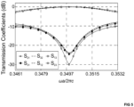
- the device's frequency response is shown in Figure 5 .
- the insertion losses are smaller than -0.05 dB, where: ⁇ is the angular frequency (in radians per second); a is the lattice constant (in meters); c is the speed of light in free space (roughly equal to 300,000,000 meters per second).
- the bandwidth (defined at the level -15 dB of isolation curves) is equal to 620MHz for excitation at port 1, 680MHz for excitation at port 2 and 730MHz for excitation at port 3.
Landscapes
- Physics & Mathematics (AREA)
- Optics & Photonics (AREA)
- General Physics & Mathematics (AREA)
- Engineering & Computer Science (AREA)
- Nonlinear Science (AREA)
- Chemical & Material Sciences (AREA)
- Nanotechnology (AREA)
- Power Engineering (AREA)
- Life Sciences & Earth Sciences (AREA)
- Crystallography & Structural Chemistry (AREA)
- Biophysics (AREA)
- Optical Integrated Circuits (AREA)
- Optical Modulation, Optical Deflection, Nonlinear Optics, Optical Demodulation, Optical Logic Elements (AREA)
Description
- The present invention refers to a T-shaped circulator with low symmetry based on a two-dimensional photonic crystal with square lattice.
- Photonic crystals are periodic structures built with materials that have different refractive indices. In such structures, there is a forbidden range of frequencies, known as photonic band gap. Electromagnetic waves with frequency located within this range are reflected by the crystal. The occurrence of this phenomenon is exploited for the design of most devices that are based on photonic crystals.
- Nonreciprocal components such as circulators and isolators are used in communication systems to reduce undesirable reflections that cause instability in generators and amplifiers, as well as loss of performance in these systems.
- Because of the nonreciprocity, circulators carry out the transmission of electromagnetic signals in one direction (clockwise or counterclockwise) determined by the sign (positive or negative) of an applied DC magnetic field. Thus, in a 3-port circulator, for example, there may be the following modes of operation (input port → output port): 1 → 2, 2 → 3 and 3 → 1 (clockwise); or 1 → 3, 3 → 2 e 2 → 1 (counterclockwise). In an ideal circulator, the power of the signal present at the input port is entirely transferred to the output port (without loss).
- As a result of researches related to the development of new devices based on photonic crystals, some patents related to circulators based on these structures have been deposited.
- For example, the circulator referred in the patent
US20120243844 is built on a two-dimensional photonic crystal with triangular lattice, consisting of holes filled with air and etched in a dielectric material. Its resonant cavity is comprised of a magneto-optical rod and of holes with changed diameters (when compared to other holes of the photonic crystal). The device in question has three ports. - The report describing the patent
US20120251048 refers to a circulator with four ports, based on the coupling of two resonant cavities. Both cavities are formed by a magneto-optical rod and by holes with modified diameters. - On the other hand, the patent
US20130223805 and the scientific document entitled "T-shaped optical circulator based on coupled magneto-optical rods and a side-coupled cavity in a square-lattice photonic crystal" (Qiong Wang et al., Physics Letters A, vol. 376, no. 4, 12 November 2011, pages 646-649), relate to a circulator built on a two-dimensional photonic crystal with square lattice of holes filled with air, etched in a dielectric material. The resonant cavity of this circulator is characterized by having four magneto-optical rods surrounding a central dielectric rod and three dielectric rods with modified diameters. Scientific document entitled "Compact three-port optical two-dimensional photonic crystal-based circulator of W-format" (Victor Dmitriev et al., Optics Letters, vol. 37, no. 15, 1 August 2012, pages 3192-3194) disclose a three-port W-shaped circulator. Patent documentsCN104101947-A andCN104101947-A respectively disclose a three-port and a four-port circulator, both having a working principle related to the excitation of electromagnetic vortices in their respective resonant cavities. - All these devices are used mainly to perform the isolation function, that is, the protection of signal sources against parasitic reflections coming from not matched loads connected to a communication system.
- In a circulator with three ports, for example, assuming that port 1 is connected to a signal source (input), port 2 is connected to the circuit that will receive the signal from the signal source (output), and port 3 is connected to an ideally matched load, the circulator will operate as following.
- Considering the clockwise propagation (1 → 2, 2 → 3 and 3 → 1), the signal coming from input (port 1) is sent to output (port 2). However, parasitic reflections that might be originated at the output (port 2) do not return to input (port 1). They will be directed to port 3, in which is connected an ideally matched load that absorb them, protecting the signal source connected to port 1.
- The proposed device, based on photonic crystal technology, can be built with reduced dimensions, favoring an increase in the integration density of components in communication systems.
- When compared to the aforementioned circulators, the present circulator has a resonant cavity with simplified geometry, making it more feasible from the point of view of construction and mass production. Moreover, it has reduced losses.
- The magnetization circuit of the proposed circulator is simplified, since the circulator in question operates with uniform magnetization and an electromagnet is able to fulfill this function. The intensity of the magnetic field generated by the electromagnet is proportional to the intensity of the current flowing through it.
- Among the performance characteristics of the developed circulator, there are the low insertion losses between input and output, high isolation levels in relation to parasitic reflections arising from the output and the wide operating band.
- In general, the developed device is based on a two-dimensional photonic crystal composed of a square lattice of dielectric rods immersed in air. In this crystal, two types of defects are inserted, namely:
- a) Removal of rows of rods (linear defects), which originates the waveguides;
- b) Changes in radius, position and refractive index of the dielectric rods located in the center of the device (local defects), which originate its resonant cavity.
- More specifically, the device has the following characteristics:
- a) At the operating central frequency 100 GHz, the lattice constant of the crystal (a) is equal to 1.065 mm;
- b) The radius of the cylinders belonging to the crystal lattice is equal to 0.2a;
- c) The three waveguides are inserted through the creation of three linear defects;
- d) The resonant cavity is formed by one central ferrite cylinder and two dielectric cylinders near the ferrite cylinder with increased diameters. The central cylinder is made from a nickel-zinc based ferrite, and it is inserted into a displaced position in relation to the axis of the horizontal waveguides.
- e) The ferrite is a gyrotropic material being described by the following expressions for the permittivity and the magnetic permeability:
- f)

- a) ε is the electrical permittivity of the material (in Farads per meter);
- b) ε0 is the permittivity of free space (in Farads per meter);
- c) [µ] is the magnetic permeability tensor of the material (in Henrys per meter);
- d) µ0 is the magnetic permeability of free space (in Henrys per meter);
- e) i is the imaginary unit;
- f) µ is a parameter that can be calculated from the following formula:
- g)

- h) k is a parameter that can be calculated from the following formula:
- i)

- j) The parameters ωm and ωi are defined by the following formulas:
- k) ωm = γM0 and ωi = γH0 ;
- l) M0 is the saturation magnetization (398 kA/m), γ is the gyromagnetic ratio (2.33 × 10⁵ rad/s per A/m), α is the damping factor (0.03175), ω is the angular frequency (rad/s) and H0 is the applied DC magnetic field (kA/m).
- m) The value of the ratio "k/µ" is equal to 0.17.
-
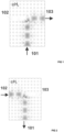
Figure 1 shows the Ez component of the electromagnetic field in the device when the input signal is applied to thewaveguide 101. -
Figure 2 shows the Ez component of the electromagnetic field in the device when the input signal is applied to thewaveguide 102. -
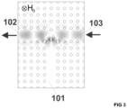
Figure 3 shows the Ez component of the electromagnetic field in the device when the input signal is applied to thewaveguide 103. -
Figure 4 shows, schematically, details of the geometry of the resonant cavity which is part of the device. -
Figure 5 shows the device frequency response. - When the excitation is applied at port 1 (associated with the waveguide 101), it occurs the signal transmission from this port to port 3 (associated with the waveguide 103), with isolation of port 2 (associated with the waveguide 102) due to the special alignment of the dipole mode, as can be seen in
figure 1 ; Similarly, when the input signal is applied in ports 2 (Figure 2 ) and3 (Figure 3 ), it is transferred to ports 1 (with isolation of port 3) and 2 (with isolation of port 1), respectively. This case corresponds to the propagation in counterclockwise direction. If the sign of the external DC magnetic field H0 is inverted, the signal propagation takes place in the clockwise direction (1 → 2, 2 → 3 and 3 → 1). - In the cases illustrated in
Figures 1 and 2 , it can be seen that the stationary dipole excited in the resonant cavity mode is rotated by an angle of 45°, which provides isolation of ports 2 and 3, respectively. On the other hand, in the case illustrated inFigure 3 , it is shown that the stationary dipole mode suffers no rotation, causing the transmission of the input signal (applied to port 3) to port 2, with isolation of the port 1. - In order to obtain a higher bandwidth, adjustments were made in the central structure of the device, which can be seen in
figure 4 . The radius of thecylinder 401 was increased by 0,10562a and the offset relative to the axis ofwaveguides 102 and 103 (Δy1) is 0,69086a. Thecylinder 402 has its radius reduced by 0,01249a and it was moved vertically, relatively to the axis of the upper cylinders (Δy2), by 0,2563a. The radii of thecylinders - The device's frequency response is shown in
Figure 5 . At the normalized central frequency ωa/2πc = 0.3499, the insertion losses are smaller than -0.05 dB, where: ω is the angular frequency (in radians per second); a is the lattice constant (in meters); c is the speed of light in free space (roughly equal to 300,000,000 meters per second). In the frequency band located around 100 GHz, the bandwidth (defined at the level -15 dB of isolation curves) is equal to 620MHz for excitation at port 1, 680MHz for excitation at port 2 and 730MHz for excitation at port 3.
Claims (2)
- A T-shaped circulator, comprising a two-dimensional photonic crystal composed of a square lattice of dielectric cylinders immersed in air in which an arrangement of waveguides and one resonant cavity are inserted, wherein the arrangement of waveguides consists of three waveguides (101, 102, 103) inserted through the removal of rows of dielectric cylinders and disposed in T-shape, two horizontal waveguides (102, 103) and one vertical waveguide (101), and the resonant cavity is disposed at the junction of the three waveguides, to perform the transmission of electromagnetic signals in a given direction, clockwise or counterclockwise, with the direction being determined by the sign of an external DC magnetic field applied to the circulator;wherein the resonant cavity is formed by an arrangement of cylinders consisting of a central ferrite cylinder (401) made from a nickel-zinc based ferrite and disposed on the axis of the vertical waveguide (101), two dielectric cylinders (403, 404) disposed near the central ferrite cylinder, wherein the diameters of the two dielectric cylinders (403, 404) are increased when compared to the diameter of the dielectric cylinders of the square lattice;wherein the central ferrite cylinder (401) is inserted into a position displaced vertically in relation to the axis of the horizontal waveguides (102, 103); andwherein the lattice constant of the photonic crystal (a) is equal to 1.065mm and the radius of the dielectric cylinders belonging to the square lattice is equal to 0.2 a, wherein a is the lattice constant of the photonic crystal.
- The T-shaped circulator of claim 1, wherein the resonant cavity is further formed by a cylinder (402) with a diameter reduced by 0.01249*a, when compared to the diameter of the dielectric cylinders of the square lattice, and which is disposed on the axis of the vertical waveguide (101) and displaced vertically relatively to the horizontal axis passing through the center of the cylinders of the square lattice located immediately above the horizontal waveguides (102, 103) by 0.2563*a towards the axis of the horizontal waveguides (102, 103),and wherein the radius of the central ferrite cylinder (401) is increased by 0.10562·a and the radii of the two dielectric cylinders (403, 404) are increased by 0.07439·a when compared to the diameter of the dielectric cylinders of the square lattice;wherein the offset (Δy1) of the central ferrite cylinder relative to the axis of the waveguides (102,103) is 0.69086 a.
Applications Claiming Priority (2)
| Application Number | Priority Date | Filing Date | Title |
|---|---|---|---|
| BR102015010964A BR102015010964A2 (en) | 2015-04-29 | 2015-04-29 | t-circulator based on a two-dimensional square lattice photonic crystal |
| PCT/BR2016/050098 WO2016172780A1 (en) | 2015-04-29 | 2016-04-29 | Circulator based on a two-dimensional photonic crystal with a square lattice |
Publications (3)
| Publication Number | Publication Date |
|---|---|
| EP3290978A1 EP3290978A1 (en) | 2018-03-07 |
| EP3290978A4 EP3290978A4 (en) | 2018-05-16 |
| EP3290978B1 true EP3290978B1 (en) | 2023-05-17 |
Family
ID=57197794
Family Applications (1)
| Application Number | Title | Priority Date | Filing Date |
|---|---|---|---|
| EP16785698.8A Active EP3290978B1 (en) | 2015-04-29 | 2016-04-29 | Circulator based on a two-dimensional photonic crystal with a square lattice |
Country Status (4)
| Country | Link |
|---|---|
| US (1) | US10168557B2 (en) |
| EP (1) | EP3290978B1 (en) |
| BR (1) | BR102015010964A2 (en) |
| WO (1) | WO2016172780A1 (en) |
Families Citing this family (5)
| Publication number | Priority date | Publication date | Assignee | Title |
|---|---|---|---|---|
| CN107908021A (en) * | 2017-11-27 | 2018-04-13 | 深圳大学 | T font photonic crystal circulators based on photonic crystal waveguide |
| CN109471275A (en) * | 2018-11-27 | 2019-03-15 | 深圳市继光科技有限公司 | A kind of three port photon crystal rings row devices |
| CN114325935B (en) * | 2021-12-08 | 2024-04-16 | 南京邮电大学 | Non-magnetic photon crystal non-reciprocal double-channel narrow-band filter |
| CN115566384B (en) * | 2022-09-09 | 2025-05-30 | 电子科技大学 | A highly efficient electromagnetic waveguide based on topological chiral boundary states |
| CN116068696B (en) * | 2023-03-03 | 2023-06-23 | 深圳麦赫科技有限公司 | Flat-plate photonic crystal circulator |
Family Cites Families (7)
| Publication number | Priority date | Publication date | Assignee | Title |
|---|---|---|---|---|
| US7489846B2 (en) * | 2004-03-11 | 2009-02-10 | Agilent Technologies, Inc. | Photonic crystal sensors |
| CN101726873B (en) * | 2009-12-14 | 2012-08-08 | 深圳大学 | Photonic crystal three-port circulator |
| CN101788727B (en) | 2009-12-14 | 2011-11-09 | 深圳大学 | Photonic crystal four-port circulator based on magneto-optical cavity coupling |
| US8731360B2 (en) * | 2010-11-12 | 2014-05-20 | Shenzhen University | Photonic crystal magneto-optical circulator and manufacturing method thereof |
| BR102013018869B1 (en) * | 2013-06-25 | 2022-06-07 | Universidade Federal Do Pará | Non-reciprocal divider by three based on a magneto-optical resonator |
| CN104101948B (en) | 2014-07-28 | 2017-04-12 | 欧阳征标 | Photonic crystal waveguide based cross circulator |
| CN104101947B (en) * | 2014-07-28 | 2017-07-04 | 欧阳征标 | The compact T fonts circulator of ultra high efficiency based on photon crystal wave-guide |
-
2015
- 2015-04-29 BR BR102015010964A patent/BR102015010964A2/en not_active Application Discontinuation
-
2016
- 2016-04-29 US US15/570,294 patent/US10168557B2/en active Active
- 2016-04-29 EP EP16785698.8A patent/EP3290978B1/en active Active
- 2016-04-29 WO PCT/BR2016/050098 patent/WO2016172780A1/en not_active Ceased
Also Published As
| Publication number | Publication date |
|---|---|
| US10168557B2 (en) | 2019-01-01 |
| US20180120598A1 (en) | 2018-05-03 |
| WO2016172780A1 (en) | 2016-11-03 |
| BR102015010964A2 (en) | 2016-11-01 |
| EP3290978A4 (en) | 2018-05-16 |
| EP3290978A1 (en) | 2018-03-07 |
Similar Documents
| Publication | Publication Date | Title |
|---|---|---|
| US7689068B1 (en) | One-way waveguides using gyrotropic photonic crystals | |
| Sundar et al. | Compact four-port circulator based on 2D photonic crystals with a 90° rotation of the light wave for photonic integrated circuits applications | |
| US10168557B2 (en) | T-shaped circulator based on a two-dimensional photonic crystal with a square lattice | |
| US10331009B2 (en) | Compact optical key based on a two-dimensional photonic crystal with 120 degree folding | |
| Fernandes et al. | Topological origin of electromagnetic energy sinks | |
| US9778496B2 (en) | Nonreciprocal three-way divider based on a magneto-optical resonator | |
| Wang et al. | Low-loss Y-junction two-dimensional magneto-photonic crystals circulator using a ferrite cylinder | |
| Zhang et al. | Design of nonreciprocal waveguide devices based on two-dimensional magneto-optical photonic crystals | |
| Umamaheswari et al. | Exploration of photonic crystal circulator based on gyromagnetic properties and scaling of ferrite materials | |
| JP6717806B2 (en) | Compact optical switch based on two-dimensional photonic crystal with 60 degree bend | |
| CN109471275A (en) | A kind of three port photon crystal rings row devices | |
| Xu et al. | Wideband Y-type circulator based on magneto photonic crystals and triangular ferrites | |
| US10641974B2 (en) | Optical three-port fork-like circulator based on a two-dimensional photonic crystal with a triangular lattice | |
| Wang et al. | Broadband six-port circulator based on magneto-optical-rod ring in photonic crystal | |
| Esmaieli et al. | Magneto-optical photonic crystal 1× 3 switchable power divider | |
| Wang et al. | Microwave-frequency experiment validation of a novel magneto-photonic crystals circulator | |
| Bi et al. | Magnetically tunable microwave bandpass filter structure composed of ferrite rods and metallic slits | |
| Wang et al. | Experimental evidence of the large photonic band gap in two‐dimensional square‐lattice Al2O3 rods array | |
| Pardavi‐Horvath | Ferrite‐Based Electronic Bandgap Heterostructures and Metamaterials | |
| EP3206063B1 (en) | Multifunctional optical device based on a two-dimensional photonic crystal and a magnetooptic resonator | |
| CN110646958A (en) | Multi-channel signal selector based on magneto-optical medium and PT symmetrical structure and using method thereof | |
| Sen et al. | Poynting Vector Spin in Gyromagnetic Medium and its Impact on Backward Power Flow in Waveguiding Structures | |
| Zhang et al. | A Hybrid Topological Heterostructure for Communication | |
| Milosevic et al. | EIT-like response in asymmetrically coupled split ring resonators | |
| CN103744199A (en) | Two-dimensional photonic crystal beam splitter and beam splitting method for same |
Legal Events
| Date | Code | Title | Description |
|---|---|---|---|
| STAA | Information on the status of an ep patent application or granted ep patent |
Free format text: STATUS: THE INTERNATIONAL PUBLICATION HAS BEEN MADE |
|
| PUAI | Public reference made under article 153(3) epc to a published international application that has entered the european phase |
Free format text: ORIGINAL CODE: 0009012 |
|
| STAA | Information on the status of an ep patent application or granted ep patent |
Free format text: STATUS: REQUEST FOR EXAMINATION WAS MADE |
|
| 17P | Request for examination filed |
Effective date: 20171108 |
|
| AK | Designated contracting states |
Kind code of ref document: A1 Designated state(s): AL AT BE BG CH CY CZ DE DK EE ES FI FR GB GR HR HU IE IS IT LI LT LU LV MC MK MT NL NO PL PT RO RS SE SI SK SM TR |
|
| AX | Request for extension of the european patent |
Extension state: BA ME |
|
| A4 | Supplementary search report drawn up and despatched |
Effective date: 20180416 |
|
| RIC1 | Information provided on ipc code assigned before grant |
Ipc: G02B 6/122 20060101ALI20180410BHEP Ipc: G02F 1/095 20060101AFI20180410BHEP |
|
| DAV | Request for validation of the european patent (deleted) | ||
| DAX | Request for extension of the european patent (deleted) | ||
| STAA | Information on the status of an ep patent application or granted ep patent |
Free format text: STATUS: EXAMINATION IS IN PROGRESS |
|
| 17Q | First examination report despatched |
Effective date: 20200206 |
|
| GRAP | Despatch of communication of intention to grant a patent |
Free format text: ORIGINAL CODE: EPIDOSNIGR1 |
|
| STAA | Information on the status of an ep patent application or granted ep patent |
Free format text: STATUS: GRANT OF PATENT IS INTENDED |
|
| INTG | Intention to grant announced |
Effective date: 20221206 |
|
| GRAS | Grant fee paid |
Free format text: ORIGINAL CODE: EPIDOSNIGR3 |
|
| GRAA | (expected) grant |
Free format text: ORIGINAL CODE: 0009210 |
|
| STAA | Information on the status of an ep patent application or granted ep patent |
Free format text: STATUS: THE PATENT HAS BEEN GRANTED |
|
| AK | Designated contracting states |
Kind code of ref document: B1 Designated state(s): AL AT BE BG CH CY CZ DE DK EE ES FI FR GB GR HR HU IE IS IT LI LT LU LV MC MK MT NL NO PL PT RO RS SE SI SK SM TR |
|
| REG | Reference to a national code |
Ref country code: GB Ref legal event code: FG4D |
|
| REG | Reference to a national code |
Ref country code: CH Ref legal event code: EP |
|
| REG | Reference to a national code |
Ref country code: DE Ref legal event code: R096 Ref document number: 602016079497 Country of ref document: DE |
|
| REG | Reference to a national code |
Ref country code: IE Ref legal event code: FG4D |
|
| REG | Reference to a national code |
Ref country code: AT Ref legal event code: REF Ref document number: 1568624 Country of ref document: AT Kind code of ref document: T Effective date: 20230615 |
|
| REG | Reference to a national code |
Ref country code: LT Ref legal event code: MG9D |
|
| REG | Reference to a national code |
Ref country code: NL Ref legal event code: MP Effective date: 20230517 |
|
| REG | Reference to a national code |
Ref country code: AT Ref legal event code: MK05 Ref document number: 1568624 Country of ref document: AT Kind code of ref document: T Effective date: 20230517 |
|
| PG25 | Lapsed in a contracting state [announced via postgrant information from national office to epo] |
Ref country code: SE Free format text: LAPSE BECAUSE OF FAILURE TO SUBMIT A TRANSLATION OF THE DESCRIPTION OR TO PAY THE FEE WITHIN THE PRESCRIBED TIME-LIMIT Effective date: 20230517 Ref country code: PT Free format text: LAPSE BECAUSE OF FAILURE TO SUBMIT A TRANSLATION OF THE DESCRIPTION OR TO PAY THE FEE WITHIN THE PRESCRIBED TIME-LIMIT Effective date: 20230918 Ref country code: NO Free format text: LAPSE BECAUSE OF FAILURE TO SUBMIT A TRANSLATION OF THE DESCRIPTION OR TO PAY THE FEE WITHIN THE PRESCRIBED TIME-LIMIT Effective date: 20230817 Ref country code: NL Free format text: LAPSE BECAUSE OF FAILURE TO SUBMIT A TRANSLATION OF THE DESCRIPTION OR TO PAY THE FEE WITHIN THE PRESCRIBED TIME-LIMIT Effective date: 20230517 Ref country code: ES Free format text: LAPSE BECAUSE OF FAILURE TO SUBMIT A TRANSLATION OF THE DESCRIPTION OR TO PAY THE FEE WITHIN THE PRESCRIBED TIME-LIMIT Effective date: 20230517 Ref country code: AT Free format text: LAPSE BECAUSE OF FAILURE TO SUBMIT A TRANSLATION OF THE DESCRIPTION OR TO PAY THE FEE WITHIN THE PRESCRIBED TIME-LIMIT Effective date: 20230517 |
|
| PG25 | Lapsed in a contracting state [announced via postgrant information from national office to epo] |
Ref country code: RS Free format text: LAPSE BECAUSE OF FAILURE TO SUBMIT A TRANSLATION OF THE DESCRIPTION OR TO PAY THE FEE WITHIN THE PRESCRIBED TIME-LIMIT Effective date: 20230517 Ref country code: PL Free format text: LAPSE BECAUSE OF FAILURE TO SUBMIT A TRANSLATION OF THE DESCRIPTION OR TO PAY THE FEE WITHIN THE PRESCRIBED TIME-LIMIT Effective date: 20230517 Ref country code: LV Free format text: LAPSE BECAUSE OF FAILURE TO SUBMIT A TRANSLATION OF THE DESCRIPTION OR TO PAY THE FEE WITHIN THE PRESCRIBED TIME-LIMIT Effective date: 20230517 Ref country code: LT Free format text: LAPSE BECAUSE OF FAILURE TO SUBMIT A TRANSLATION OF THE DESCRIPTION OR TO PAY THE FEE WITHIN THE PRESCRIBED TIME-LIMIT Effective date: 20230517 Ref country code: IS Free format text: LAPSE BECAUSE OF FAILURE TO SUBMIT A TRANSLATION OF THE DESCRIPTION OR TO PAY THE FEE WITHIN THE PRESCRIBED TIME-LIMIT Effective date: 20230917 Ref country code: HR Free format text: LAPSE BECAUSE OF FAILURE TO SUBMIT A TRANSLATION OF THE DESCRIPTION OR TO PAY THE FEE WITHIN THE PRESCRIBED TIME-LIMIT Effective date: 20230517 Ref country code: GR Free format text: LAPSE BECAUSE OF FAILURE TO SUBMIT A TRANSLATION OF THE DESCRIPTION OR TO PAY THE FEE WITHIN THE PRESCRIBED TIME-LIMIT Effective date: 20230818 |
|
| PG25 | Lapsed in a contracting state [announced via postgrant information from national office to epo] |
Ref country code: FI Free format text: LAPSE BECAUSE OF FAILURE TO SUBMIT A TRANSLATION OF THE DESCRIPTION OR TO PAY THE FEE WITHIN THE PRESCRIBED TIME-LIMIT Effective date: 20230517 |
|
| PG25 | Lapsed in a contracting state [announced via postgrant information from national office to epo] |
Ref country code: SK Free format text: LAPSE BECAUSE OF FAILURE TO SUBMIT A TRANSLATION OF THE DESCRIPTION OR TO PAY THE FEE WITHIN THE PRESCRIBED TIME-LIMIT Effective date: 20230517 |
|
| PG25 | Lapsed in a contracting state [announced via postgrant information from national office to epo] |
Ref country code: SM Free format text: LAPSE BECAUSE OF FAILURE TO SUBMIT A TRANSLATION OF THE DESCRIPTION OR TO PAY THE FEE WITHIN THE PRESCRIBED TIME-LIMIT Effective date: 20230517 Ref country code: SK Free format text: LAPSE BECAUSE OF FAILURE TO SUBMIT A TRANSLATION OF THE DESCRIPTION OR TO PAY THE FEE WITHIN THE PRESCRIBED TIME-LIMIT Effective date: 20230517 Ref country code: RO Free format text: LAPSE BECAUSE OF FAILURE TO SUBMIT A TRANSLATION OF THE DESCRIPTION OR TO PAY THE FEE WITHIN THE PRESCRIBED TIME-LIMIT Effective date: 20230517 Ref country code: EE Free format text: LAPSE BECAUSE OF FAILURE TO SUBMIT A TRANSLATION OF THE DESCRIPTION OR TO PAY THE FEE WITHIN THE PRESCRIBED TIME-LIMIT Effective date: 20230517 Ref country code: DK Free format text: LAPSE BECAUSE OF FAILURE TO SUBMIT A TRANSLATION OF THE DESCRIPTION OR TO PAY THE FEE WITHIN THE PRESCRIBED TIME-LIMIT Effective date: 20230517 Ref country code: CZ Free format text: LAPSE BECAUSE OF FAILURE TO SUBMIT A TRANSLATION OF THE DESCRIPTION OR TO PAY THE FEE WITHIN THE PRESCRIBED TIME-LIMIT Effective date: 20230517 |
|
| REG | Reference to a national code |
Ref country code: DE Ref legal event code: R097 Ref document number: 602016079497 Country of ref document: DE |
|
| PLBE | No opposition filed within time limit |
Free format text: ORIGINAL CODE: 0009261 |
|
| STAA | Information on the status of an ep patent application or granted ep patent |
Free format text: STATUS: NO OPPOSITION FILED WITHIN TIME LIMIT |
|
| 26N | No opposition filed |
Effective date: 20240220 |
|
| PG25 | Lapsed in a contracting state [announced via postgrant information from national office to epo] |
Ref country code: SI Free format text: LAPSE BECAUSE OF FAILURE TO SUBMIT A TRANSLATION OF THE DESCRIPTION OR TO PAY THE FEE WITHIN THE PRESCRIBED TIME-LIMIT Effective date: 20230517 |
|
| PG25 | Lapsed in a contracting state [announced via postgrant information from national office to epo] |
Ref country code: SI Free format text: LAPSE BECAUSE OF FAILURE TO SUBMIT A TRANSLATION OF THE DESCRIPTION OR TO PAY THE FEE WITHIN THE PRESCRIBED TIME-LIMIT Effective date: 20230517 Ref country code: IT Free format text: LAPSE BECAUSE OF FAILURE TO SUBMIT A TRANSLATION OF THE DESCRIPTION OR TO PAY THE FEE WITHIN THE PRESCRIBED TIME-LIMIT Effective date: 20230517 |
|
| REG | Reference to a national code |
Ref country code: DE Ref legal event code: R119 Ref document number: 602016079497 Country of ref document: DE |
|
| PG25 | Lapsed in a contracting state [announced via postgrant information from national office to epo] |
Ref country code: BG Free format text: LAPSE BECAUSE OF FAILURE TO SUBMIT A TRANSLATION OF THE DESCRIPTION OR TO PAY THE FEE WITHIN THE PRESCRIBED TIME-LIMIT Effective date: 20230517 |
|
| PG25 | Lapsed in a contracting state [announced via postgrant information from national office to epo] |
Ref country code: MC Free format text: LAPSE BECAUSE OF FAILURE TO SUBMIT A TRANSLATION OF THE DESCRIPTION OR TO PAY THE FEE WITHIN THE PRESCRIBED TIME-LIMIT Effective date: 20230517 |
|
| PG25 | Lapsed in a contracting state [announced via postgrant information from national office to epo] |
Ref country code: MC Free format text: LAPSE BECAUSE OF FAILURE TO SUBMIT A TRANSLATION OF THE DESCRIPTION OR TO PAY THE FEE WITHIN THE PRESCRIBED TIME-LIMIT Effective date: 20230517 Ref country code: BG Free format text: LAPSE BECAUSE OF FAILURE TO SUBMIT A TRANSLATION OF THE DESCRIPTION OR TO PAY THE FEE WITHIN THE PRESCRIBED TIME-LIMIT Effective date: 20230517 |
|
| REG | Reference to a national code |
Ref country code: CH Ref legal event code: PL |
|
| PG25 | Lapsed in a contracting state [announced via postgrant information from national office to epo] |
Ref country code: LU Free format text: LAPSE BECAUSE OF NON-PAYMENT OF DUE FEES Effective date: 20240429 |
|
| GBPC | Gb: european patent ceased through non-payment of renewal fee |
Effective date: 20240429 |
|
| REG | Reference to a national code |
Ref country code: BE Ref legal event code: MM Effective date: 20240430 |
|
| PG25 | Lapsed in a contracting state [announced via postgrant information from national office to epo] |
Ref country code: LU Free format text: LAPSE BECAUSE OF NON-PAYMENT OF DUE FEES Effective date: 20240429 |
|
| PG25 | Lapsed in a contracting state [announced via postgrant information from national office to epo] |
Ref country code: DE Free format text: LAPSE BECAUSE OF NON-PAYMENT OF DUE FEES Effective date: 20241105 |
|
| PG25 | Lapsed in a contracting state [announced via postgrant information from national office to epo] |
Ref country code: BE Free format text: LAPSE BECAUSE OF NON-PAYMENT OF DUE FEES Effective date: 20240430 |
|
| PG25 | Lapsed in a contracting state [announced via postgrant information from national office to epo] |
Ref country code: GB Free format text: LAPSE BECAUSE OF NON-PAYMENT OF DUE FEES Effective date: 20240429 |
|
| PG25 | Lapsed in a contracting state [announced via postgrant information from national office to epo] |
Ref country code: FR Free format text: LAPSE BECAUSE OF NON-PAYMENT OF DUE FEES Effective date: 20240430 |
|
| PG25 | Lapsed in a contracting state [announced via postgrant information from national office to epo] |
Ref country code: GB Free format text: LAPSE BECAUSE OF NON-PAYMENT OF DUE FEES Effective date: 20240429 Ref country code: FR Free format text: LAPSE BECAUSE OF NON-PAYMENT OF DUE FEES Effective date: 20240430 Ref country code: DE Free format text: LAPSE BECAUSE OF NON-PAYMENT OF DUE FEES Effective date: 20241105 Ref country code: BE Free format text: LAPSE BECAUSE OF NON-PAYMENT OF DUE FEES Effective date: 20240430 Ref country code: CH Free format text: LAPSE BECAUSE OF NON-PAYMENT OF DUE FEES Effective date: 20240430 |
|
| PG25 | Lapsed in a contracting state [announced via postgrant information from national office to epo] |
Ref country code: IE Free format text: LAPSE BECAUSE OF NON-PAYMENT OF DUE FEES Effective date: 20240429 |
|
| PG25 | Lapsed in a contracting state [announced via postgrant information from national office to epo] |
Ref country code: CY Free format text: LAPSE BECAUSE OF FAILURE TO SUBMIT A TRANSLATION OF THE DESCRIPTION OR TO PAY THE FEE WITHIN THE PRESCRIBED TIME-LIMIT; INVALID AB INITIO Effective date: 20160429 |
|
| PG25 | Lapsed in a contracting state [announced via postgrant information from national office to epo] |
Ref country code: HU Free format text: LAPSE BECAUSE OF FAILURE TO SUBMIT A TRANSLATION OF THE DESCRIPTION OR TO PAY THE FEE WITHIN THE PRESCRIBED TIME-LIMIT; INVALID AB INITIO Effective date: 20160429 |
|
| PG25 | Lapsed in a contracting state [announced via postgrant information from national office to epo] |
Ref country code: TR Free format text: LAPSE BECAUSE OF FAILURE TO SUBMIT A TRANSLATION OF THE DESCRIPTION OR TO PAY THE FEE WITHIN THE PRESCRIBED TIME-LIMIT Effective date: 20230517 |