EP3290258A2 - Energy storage device - Google Patents
Energy storage device Download PDFInfo
- Publication number
- EP3290258A2 EP3290258A2 EP17188372.1A EP17188372A EP3290258A2 EP 3290258 A2 EP3290258 A2 EP 3290258A2 EP 17188372 A EP17188372 A EP 17188372A EP 3290258 A2 EP3290258 A2 EP 3290258A2
- Authority
- EP
- European Patent Office
- Prior art keywords
- bridge
- terminal
- inductor
- positive
- toggle
- Prior art date
- Legal status (The legal status is an assumption and is not a legal conclusion. Google has not performed a legal analysis and makes no representation as to the accuracy of the status listed.)
- Granted
Links
- 238000004146 energy storage Methods 0.000 title claims abstract description 8
- 239000003990 capacitor Substances 0.000 claims description 15
- 230000002457 bidirectional effect Effects 0.000 description 11
- 238000010586 diagram Methods 0.000 description 6
- 230000007704 transition Effects 0.000 description 6
- 230000007423 decrease Effects 0.000 description 4
- 238000000034 method Methods 0.000 description 3
- 230000007812 deficiency Effects 0.000 description 2
- 238000005516 engineering process Methods 0.000 description 1
- 230000000737 periodic effect Effects 0.000 description 1
- 230000001105 regulatory effect Effects 0.000 description 1
- 230000001960 triggered effect Effects 0.000 description 1
Images
Classifications
-
- H—ELECTRICITY
- H02—GENERATION; CONVERSION OR DISTRIBUTION OF ELECTRIC POWER
- H02M—APPARATUS FOR CONVERSION BETWEEN AC AND AC, BETWEEN AC AND DC, OR BETWEEN DC AND DC, AND FOR USE WITH MAINS OR SIMILAR POWER SUPPLY SYSTEMS; CONVERSION OF DC OR AC INPUT POWER INTO SURGE OUTPUT POWER; CONTROL OR REGULATION THEREOF
- H02M3/00—Conversion of dc power input into dc power output
- H02M3/02—Conversion of dc power input into dc power output without intermediate conversion into ac
- H02M3/04—Conversion of dc power input into dc power output without intermediate conversion into ac by static converters
- H02M3/10—Conversion of dc power input into dc power output without intermediate conversion into ac by static converters using discharge tubes with control electrode or semiconductor devices with control electrode
- H02M3/145—Conversion of dc power input into dc power output without intermediate conversion into ac by static converters using discharge tubes with control electrode or semiconductor devices with control electrode using devices of a triode or transistor type requiring continuous application of a control signal
- H02M3/155—Conversion of dc power input into dc power output without intermediate conversion into ac by static converters using discharge tubes with control electrode or semiconductor devices with control electrode using devices of a triode or transistor type requiring continuous application of a control signal using semiconductor devices only
- H02M3/156—Conversion of dc power input into dc power output without intermediate conversion into ac by static converters using discharge tubes with control electrode or semiconductor devices with control electrode using devices of a triode or transistor type requiring continuous application of a control signal using semiconductor devices only with automatic control of output voltage or current, e.g. switching regulators
- H02M3/158—Conversion of dc power input into dc power output without intermediate conversion into ac by static converters using discharge tubes with control electrode or semiconductor devices with control electrode using devices of a triode or transistor type requiring continuous application of a control signal using semiconductor devices only with automatic control of output voltage or current, e.g. switching regulators including plural semiconductor devices as final control devices for a single load
- H02M3/1582—Buck-boost converters
-
- B—PERFORMING OPERATIONS; TRANSPORTING
- B60—VEHICLES IN GENERAL
- B60L—PROPULSION OF ELECTRICALLY-PROPELLED VEHICLES; SUPPLYING ELECTRIC POWER FOR AUXILIARY EQUIPMENT OF ELECTRICALLY-PROPELLED VEHICLES; ELECTRODYNAMIC BRAKE SYSTEMS FOR VEHICLES IN GENERAL; MAGNETIC SUSPENSION OR LEVITATION FOR VEHICLES; MONITORING OPERATING VARIABLES OF ELECTRICALLY-PROPELLED VEHICLES; ELECTRIC SAFETY DEVICES FOR ELECTRICALLY-PROPELLED VEHICLES
- B60L2210/00—Converter types
- B60L2210/10—DC to DC converters
-
- G—PHYSICS
- G05—CONTROLLING; REGULATING
- G05F—SYSTEMS FOR REGULATING ELECTRIC OR MAGNETIC VARIABLES
- G05F1/00—Automatic systems in which deviations of an electric quantity from one or more predetermined values are detected at the output of the system and fed back to a device within the system to restore the detected quantity to its predetermined value or values, i.e. retroactive systems
- G05F1/10—Regulating voltage or current
- G05F1/46—Regulating voltage or current wherein the variable actually regulated by the final control device is dc
-
- Y—GENERAL TAGGING OF NEW TECHNOLOGICAL DEVELOPMENTS; GENERAL TAGGING OF CROSS-SECTIONAL TECHNOLOGIES SPANNING OVER SEVERAL SECTIONS OF THE IPC; TECHNICAL SUBJECTS COVERED BY FORMER USPC CROSS-REFERENCE ART COLLECTIONS [XRACs] AND DIGESTS
- Y02—TECHNOLOGIES OR APPLICATIONS FOR MITIGATION OR ADAPTATION AGAINST CLIMATE CHANGE
- Y02T—CLIMATE CHANGE MITIGATION TECHNOLOGIES RELATED TO TRANSPORTATION
- Y02T10/00—Road transport of goods or passengers
- Y02T10/60—Other road transportation technologies with climate change mitigation effect
- Y02T10/70—Energy storage systems for electromobility, e.g. batteries
-
- Y—GENERAL TAGGING OF NEW TECHNOLOGICAL DEVELOPMENTS; GENERAL TAGGING OF CROSS-SECTIONAL TECHNOLOGIES SPANNING OVER SEVERAL SECTIONS OF THE IPC; TECHNICAL SUBJECTS COVERED BY FORMER USPC CROSS-REFERENCE ART COLLECTIONS [XRACs] AND DIGESTS
- Y02—TECHNOLOGIES OR APPLICATIONS FOR MITIGATION OR ADAPTATION AGAINST CLIMATE CHANGE
- Y02T—CLIMATE CHANGE MITIGATION TECHNOLOGIES RELATED TO TRANSPORTATION
- Y02T10/00—Road transport of goods or passengers
- Y02T10/60—Other road transportation technologies with climate change mitigation effect
- Y02T10/72—Electric energy management in electromobility
Definitions
- the invention is related to electrical technology, namely to autonomous electric power supply systems, and may be used mostly in vehicles.
- micro-hybrid device for a motor vehicle (Micro-hybrid device for motor vehicle / Masson et al. // U.S. Pat. No 7,952,223 B2 - May 31, 2011 ), which uses a rechargeable current source designed as a battery of electrochemical capacitors (also known as "ultra-capacitor”), connected to the on-board network of an automobile using a direct current bidirectional converter with control unit, having a reference input, while the charge/discharge current of the rechargeable current source can be regulated by the reference input signal thus accumulating and returning electrical energy and corresponds to the claimed invention designation.
- a direct current bidirectional converter circuit does not describe the direct current bidirectional converter circuit.
- Each energy storage device consists of a rechargeable current source and bidirectional buck-boost converter, which contains a control unit, inductor, first half-bridge and second half-bridge. Each half-bridge has positive terminal, negative terminal and toggle terminal, designed to connect to either the positive or negative terminal.
- the negative terminal of the first half-bridge is connected to the negative terminal of the second half-bridge
- the toggle terminal of the first half-bridge is connected to the toggle terminal of the second half-bridge by the inductor
- the positive and negative terminals of the first and second half-bridges are the power terminals of the bidirectional buck-boost converter.
- Each half-bridge consists of two serially connected electronic switching devices, based on transistors whose gates are connected to the control unit.
- the first half-bridge is connected in parallel to the rechargeable current source by positive and negative terminals, while the second one to the vehicle's on-board network.
- An ultra-capacitor or an accumulator battery can be used as a rechargeable current source.
- the principle of the control unit for the majority of bidirectional buck-boost converters is based on the analysis of voltage values at its power terminals (buck mode, boost mode, or buck-boost mode).
- the buck-boost operating mode is triggered, when input and output voltage values at the converter's power terminals are nearly the same, and based on their analysis, it is impossible to make a clear choice between buck and boost operating modes.
- the buck-boost operating mode causes excessive commutations of electronic switching devices, which results in additional energy losses. Electrical energy storage device must ensure minimal energy losses, therefore the buck-boost operating mode is not desirable.
- control unit of the buck-boost converter (Hysteretic controlled buck-boost converter / Qiu et al. // U.S. Pat. No 8,330,435 B2 - Dec. 11, 2012 ), consisting of: first input, supplied with voltage from the inductor's current sensor output; second input, which receives error voltage; plurality of offset voltages based on the error voltage.
- the control unit selects the converter's operating mode based on the comparison of the inductor's current values with plurality of offset voltages, which helps to eliminate the buck-boost operating mode and thus reduces energy losses.
- the deficiency of this control unit is its complex circuitry, which is required due to a development of plurality of offset error voltages.
- This device consists of interface power terminals, rechargeable current source, first half-bridge, second half-bridge, inductor with inductor's current sensor and control unit, while each half-bridge has control inputs, positive terminal, negative terminal and toggle terminal, designed to connect to either the positive or negative terminal depending on signals at control inputs; the first half-bridge is connected in parallel to the rechargeable current source by positive and negative terminals, the negative terminal of the first half-bridge is connected to the negative terminal of the second half-bridge, the toggle terminal of the first half-bridge is connected to the toggle terminal of the second half-bridge by the inductor, the positive and negative terminals of the second half-bridge are the interface power terminals.
- Each half-bridge consists of two serially connected electronic switching devices, based on the transistors, which gates are the half-bridge control inputs; a diode is coupled in parallel opposition with each switching device.
- An electrochemical capacitor battery is used as a rechargeable current source.
- the prototype description does not describe the control unit circuit of the bidirectional buck-boost converter, but a control method is provided. This method provides for the converter's operating mode depending on the correlation of voltage values at interface power terminals and at rechargeable current source terminals:
- the claimed device is designed to connect, by interface power terminals, to direct current electrical network and to control the electrical energy flow through interface power terminals in order to accumulate and return it to supply high-powered intermittent loads.
- the task of the claimed device is to reduce energy losses and device simplification.
- the technical result consists of a minimization of switching during the operation of the device and a reduction of components and connections.
- the claimed energy storage device consisting of interface power terminals, rechargeable current source, first half-bridge, second half-bridge, inductor with an inductor's current sensor and control unit, while each half-bridge has a control input, positive terminal, negative terminal, and toggle terminal, designed to connect to either the positive or negative terminal depending on the signal at the control input
- the first half-bridge is connected in parallel to the rechargeable current source by positive and negative terminals
- the negative terminal of the first half-bridge is connected to the negative terminal of the second half-bridge
- the toggle terminal of the first half-bridge is connected to the toggle terminal of the second half-bridge by the inductor
- the positive and negative terminals of the second half-bridge are the interface power terminals
- the control unit has a reference input and contains first Schmitt trigger, whose output is connected to the control input of the first half-bridge, second Schmitt trigger, whose output is connected to the control input of the second half-bridge and summation circuit, whose output is connected to the inputs
- Each half-bridge is designed to connect the toggle terminal to the positive terminal based on the signal H at the control input, and to the negative terminal based on signal L at the control input, the first Schmitt trigger has threshold levels U 1 and U 2 of the toggle output in condition H and L respectively, the second Schmitt trigger has threshold levels U 3 and U 4 of the toggle output in condition H and L respectively.
- Threshold levels of Schmitt triggers are satisfied by inequalities: U 4 ⁇ U 1 ⁇ U 2 , U 4 ⁇ U 3 ⁇ U 2 , if the output signal of the inductor's current sensor is accepted as positive when the inductor's current flows in the direction from the toggle terminal of the first half-bridge to the toggle terminal of the second half-bridge.
- Threshold levels of Schmitt triggers are satisfied by inequalities: U 4 > U 1 > U 2 , U 4 > U 3 > U 2 , if the output signal of the inductor's current sensor is accepted as positive when the inductor's current flows in the direction of the toggle terminal of the second half-bridge to the toggle terminal of the first half-bridge.
- Inequalities (1,2) and (3,4) describe equivalent implementation options of the claimed device (selection of inequalities depends on the inductor's current direction, conditionally accepted as positive).
- the rechargeable current source may be designed as an electrochemical capacitor battery.
- the rechargeable current source may be designed as an accumulator battery.
- first half-bridge, second half-bridge, inductor and control unit each half-bridge has a control input, positive terminal, negative terminal, and toggle terminal, designed to connect to either the positive or negative terminal depending on the signal at the control input;
- the negative terminal of the first half-bridge is connected to the negative terminal of the second half-bridge,
- the toggle terminal of the first half-bridge is connected to the toggle terminal of the second half-bridge by the inductor
- inductor describes a bidirectional buck-boost converter.
- the control unit has a reference input and contains first Schmitt trigger, whose output is connected to the control input of the first half-bridge, second Schmitt trigger, whose output is connected to the control input of the second half-bridge and summation circuit, whose output is connected to the inputs of the first and second Schmitt triggers, the first input of the summation circuit is connected to the output of the inductor's current sensor, while the second input of the summation circuit is the reference input of the control unit” ensure the control of the current flowing through the inductor of the bidirectional buck-boost converter.
- each half-bridge is designed to connect the toggle terminal to the positive terminal based on the signal H, or to the negative terminal based on the signal L at the control input;
- the first Schmitt trigger has threshold levels U 1 and U 2 of the toggle output in condition H and L respectively;
- the second Schmitt trigger has threshold levels U 3 and U 4 of the toggle output in condition H and L respectively;
- threshold levels of Schmitt triggers are satisfied by inequalities (1,2) if the output signal of the inductor's current sensor is accepted as positive when the inductor's current flows in the direction from the toggle terminal of the first half-bridge to the toggle terminal of the second half-bridge;
- threshold levels of Schmitt triggers are satisfied by inequalities (3,4) if the output signal of the inductor's current sensor is accepted as positive when the inductor's current flows in the direction of the toggle terminal of the second half-bridge to the toggle terminal of the first half-bridge
- the minimally possible switching frequency corresponds to the maximum allowed level of the inductor's current ripple levels, which is defined by threshold levels U 1 and U 2 in the buck operating mode, or by threshold levels U 3 and U 4 in the boost operating mode.
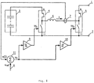
- the storage device consists of interface power outputs 1 and 2, rechargeable current source 3, first half-bridge 4, second half-bridge 5, inductor 6 with current sensor 7 and control unit.
- the control unit has the reference input 8 and contains first Schmitt trigger 9, second Schmitt trigger 10 and summation circuit 11.
- Each half-bridge 4 and 5 are designed to connect the toggle terminal to the positive terminal based on the signal H, or to the negative terminal based on signal L at the control input.
- Half-bridges 4 and 5 designs are well-known: each half-bridge has two serially connected electronic switching devices, based on the MOSFET or IGBT transistors, whose gates are linked to the half-bridge control input by drivers and logic components; a diode is coupled in parallel opposition with each switching device.
- the first half-bridge 4 is connected in parallel to the rechargeable current source 3 by positive and negative terminals, the negative terminal of the first half-bridge 4 is connected to the negative terminal of the second half-bridge 5, the toggle terminal of the first half-bridge 4 is connected to the toggle terminal of the second half-bridge 5 by the inductor 6, the positive and negative terminals of the second half-bridge 5 are the interface power terminals 1 and 2.
- the output of the first Schmitt trigger 9 is connected to the control input of the first half-bridge 4.
- the output of the second Schmitt trigger 10 is connected to the control input of the second half-bridge 5.
- the output of the summation circuit 11 is connected to inputs of Schmitt triggers 9 and 10.
- the first input of the summation circuit 11 is connected to the inductor's current sensor 7 output, while the second input of the summation circuit 11 is the reference input 8 of the control unit.
- the rechargeable current source 3 can be any two-terminal, which can accumulate energy when the charge current is flowing and return energy when the discharge current is flowing, e.g. an accumulator battery or electrochemical capacitor battery (ultra-capacitor).
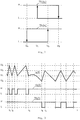
- the device operation is further clarified using the discharge example of the ultra-capacitor 3 in accordance with timing diagrams ( Fig. 3 ).
- signal u ⁇ (t) reaches U 2 value - first Schmitt trigger 9 switches and signal TS 1 (t) transition to L state.
- the referenced example shows that the claimed device ensures a clear choice between the buck and boost modes without transitioning into buck-boost mode.
- the maximum allowed level of current i ripples of the inductor is defined by transmitting parameters TS 1 (u ⁇ ) and TS 2 (u ⁇ ) of Schmitt triggers 9 and 10. Furthermore, a minimally possible switching frequency is ensured, which corresponds to the stated technical task to minimize energy losses.
- the control unit consists of less components than other known devices, which ensures device simplification.
Abstract
Description
- The invention is related to electrical technology, namely to autonomous electric power supply systems, and may be used mostly in vehicles.
- There is a micro-hybrid device for a motor vehicle (Micro-hybrid device for motor vehicle /
Masson et al. // U.S. Pat. Nº 7,952,223 B2 - May 31, 2011 ), which uses a rechargeable current source designed as a battery of electrochemical capacitors (also known as "ultra-capacitor"), connected to the on-board network of an automobile using a direct current bidirectional converter with control unit, having a reference input, while the charge/discharge current of the rechargeable current source can be regulated by the reference input signal thus accumulating and returning electrical energy and corresponds to the claimed invention designation. However, the description of this device does not describe the direct current bidirectional converter circuit. - There is an automotive electrical power supply system (Automotive electrical system configuration /
O'Gorman et al. // U.S. Pat. Nº 8,159,083 B2 - Apr. 17, 2012 ), which uses electrical energy storage devices. Each energy storage device consists of a rechargeable current source and bidirectional buck-boost converter, which contains a control unit, inductor, first half-bridge and second half-bridge. Each half-bridge has positive terminal, negative terminal and toggle terminal, designed to connect to either the positive or negative terminal. The negative terminal of the first half-bridge is connected to the negative terminal of the second half-bridge, the toggle terminal of the first half-bridge is connected to the toggle terminal of the second half-bridge by the inductor, the positive and negative terminals of the first and second half-bridges are the power terminals of the bidirectional buck-boost converter. Each half-bridge consists of two serially connected electronic switching devices, based on transistors whose gates are connected to the control unit. The first half-bridge is connected in parallel to the rechargeable current source by positive and negative terminals, while the second one to the vehicle's on-board network. An ultra-capacitor or an accumulator battery can be used as a rechargeable current source. - These devices regulate the charge/discharge current parameters of the rechargeable current source, which allows to accumulate and return electric energy and corresponds to the claimed invention designation. However, its description does not describe the control unit circuit of the bidirectional buck-boost converter.
- The principle of the control unit for the majority of bidirectional buck-boost converters (e.g. Control circuit and method for maintaining high efficiency in a buck-boost switching regulator /
Dwelley et al. // U.S. Pat. Nº 6,166,527 - Dec. 26, 2000 ) is based on the analysis of voltage values at its power terminals (buck mode, boost mode, or buck-boost mode). The buck-boost operating mode is triggered, when input and output voltage values at the converter's power terminals are nearly the same, and based on their analysis, it is impossible to make a clear choice between buck and boost operating modes. - The buck-boost operating mode causes excessive commutations of electronic switching devices, which results in additional energy losses. Electrical energy storage device must ensure minimal energy losses, therefore the buck-boost operating mode is not desirable.
- There is a control unit of the buck-boost converter (Hysteretic controlled buck-boost converter /
Qiu et al. // U.S. Pat. Nº 8,330,435 B2 - Dec. 11, 2012 ), consisting of: first input, supplied with voltage from the inductor's current sensor output; second input, which receives error voltage; plurality of offset voltages based on the error voltage. - The control unit selects the converter's operating mode based on the comparison of the inductor's current values with plurality of offset voltages, which helps to eliminate the buck-boost operating mode and thus reduces energy losses. The deficiency of this control unit is its complex circuitry, which is required due to a development of plurality of offset error voltages.
- A prototype of an energy storage device, based on the bidirectional buck-boost converter, closest by its design and technical nature to the claimed invention, was chosen (Bidirectional buck-boost converter /
Esser // U.S. Pat. Nº 5,734,258 - Mar. 31, 1998 ). This device consists of interface power terminals, rechargeable current source, first half-bridge, second half-bridge, inductor with inductor's current sensor and control unit, while each half-bridge has control inputs, positive terminal, negative terminal and toggle terminal, designed to connect to either the positive or negative terminal depending on signals at control inputs; the first half-bridge is connected in parallel to the rechargeable current source by positive and negative terminals, the negative terminal of the first half-bridge is connected to the negative terminal of the second half-bridge, the toggle terminal of the first half-bridge is connected to the toggle terminal of the second half-bridge by the inductor, the positive and negative terminals of the second half-bridge are the interface power terminals. Each half-bridge consists of two serially connected electronic switching devices, based on the transistors, which gates are the half-bridge control inputs; a diode is coupled in parallel opposition with each switching device. An electrochemical capacitor battery is used as a rechargeable current source. - The prototype description does not describe the control unit circuit of the bidirectional buck-boost converter, but a control method is provided. This method provides for the converter's operating mode depending on the correlation of voltage values at interface power terminals and at rechargeable current source terminals:
- in those cases, where stated voltage values significantly differ, a buck operating mode or boost operating mode is selected, specified by having the toggle terminal of one of the half-bridges is permanently connected to its positive terminal, while the toggle terminal of another half-bridge periodically switches between its positive and negative terminals;
- in those cases, where stated values differ insignificantly, a buck-boost operating mode is selected, specified by having toggle terminals of both half-bridges periodically switch between its positive and negative terminals.
- The deficiencies of the prototype are the following:
- the buck-boost operating mode results in additional energy losses due to the periodic switching of both half-bridges;
- required operating mode selection depending on the correlation of voltage values at interface power terminals and rechargeable current source terminals results in a complexity of the converter's control unit.
- The claimed device is designed to connect, by interface power terminals, to direct current electrical network and to control the electrical energy flow through interface power terminals in order to accumulate and return it to supply high-powered intermittent loads.
- The task of the claimed device is to reduce energy losses and device simplification.
- The technical result consists of a minimization of switching during the operation of the device and a reduction of components and connections.
- The technical result is achieved by having the claimed energy storage device, consisting of interface power terminals, rechargeable current source, first half-bridge, second half-bridge, inductor with an inductor's current sensor and control unit, while each half-bridge has a control input, positive terminal, negative terminal, and toggle terminal, designed to connect to either the positive or negative terminal depending on the signal at the control input, the first half-bridge is connected in parallel to the rechargeable current source by positive and negative terminals, the negative terminal of the first half-bridge is connected to the negative terminal of the second half-bridge, the toggle terminal of the first half-bridge is connected to the toggle terminal of the second half-bridge by the inductor, the positive and negative terminals of the second half-bridge are the interface power terminals, according to the invention, the control unit has a reference input and contains first Schmitt trigger, whose output is connected to the control input of the first half-bridge, second Schmitt trigger, whose output is connected to the control input of the second half-bridge and summation circuit, whose output is connected to the inputs of the first and second Schmitt triggers, the first input of the summation circuit is connected to the output of the inductor's current sensor, while the second input of the summation circuit is the reference input of the control unit.
- Each half-bridge is designed to connect the toggle terminal to the positive terminal based on the signal H at the control input, and to the negative terminal based on signal L at the control input, the first Schmitt trigger has threshold levels U1 and U2 of the toggle output in condition H and L respectively, the second Schmitt trigger has threshold levels U3 and U4 of the toggle output in condition H and L respectively.
- Threshold levels of Schmitt triggers are satisfied by inequalities:


- Threshold levels of Schmitt triggers are satisfied by inequalities:


- Inequalities (1,2) and (3,4) describe equivalent implementation options of the claimed device (selection of inequalities depends on the inductor's current direction, conditionally accepted as positive).
- The rechargeable current source may be designed as an electrochemical capacitor battery.
- The rechargeable current source may be designed as an accumulator battery.
- Significant features of the claimed device to achieve the technical result are listed below.
- A combination of significant features of the claimed device: "first half-bridge, second half-bridge, inductor and control unit; each half-bridge has a control input, positive terminal, negative terminal, and toggle terminal, designed to connect to either the positive or negative terminal depending on the signal at the control input; the negative terminal of the first half-bridge is connected to the negative terminal of the second half-bridge, the toggle terminal of the first half-bridge is connected to the toggle terminal of the second half-bridge by the inductor" describes a bidirectional buck-boost converter.
- Significant features of the claimed device: "the control unit has a reference input and contains first Schmitt trigger, whose output is connected to the control input of the first half-bridge, second Schmitt trigger, whose output is connected to the control input of the second half-bridge and summation circuit, whose output is connected to the inputs of the first and second Schmitt triggers, the first input of the summation circuit is connected to the output of the inductor's current sensor, while the second input of the summation circuit is the reference input of the control unit" ensure the control of the current flowing through the inductor of the bidirectional buck-boost converter.
- An ability to control the current flowing through the inductor of the -bidirectional buck-boost converter, combined with features: "the first half-bridge is connected in parallel to the rechargeable current source; the positive and negative terminals of the second half-bridge are the interface power terminals" ensures the operation of the claimed device in accordance with its design: control of the electrical energy flow through interface power terminals in order to accumulate and return it to supply high-powered intermittent loads.
- A combination of significant features: "Each half-bridge is designed to connect the toggle terminal to the positive terminal based on the signal H, or to the negative terminal based on the signal L at the control input; the first Schmitt trigger has threshold levels U1 and U2 of the toggle output in condition H and L respectively; the second Schmitt trigger has threshold levels U3 and U4 of the toggle output in condition H and L respectively; threshold levels of Schmitt triggers are satisfied by inequalities (1,2) if the output signal of the inductor's current sensor is accepted as positive when the inductor's current flows in the direction from the toggle terminal of the first half-bridge to the toggle terminal of the second half-bridge; threshold levels of Schmitt triggers are satisfied by inequalities (3,4) if the output signal of the inductor's current sensor is accepted as positive when the inductor's current flows in the direction of the toggle terminal of the second half-bridge to the toggle terminal of the first half-bridge" ensures a minimum of switching during the operation of the claimed device.
- A minimization of switching is ensured by the fact that the buck-boost operating mode is eliminated, since inequalities (1,2) and (3,4) ensure a clear choice between buck and boost modes. When there is a simultaneous reception of signals H to the logical control inputs of both half-bridges, the inductor's current increase precisely corresponds to the buck operating mode of the converter, while a current decrease corresponds to the boost operating mode of the converter.
- The minimally possible switching frequency corresponds to the maximum allowed level of the inductor's current ripple levels, which is defined by threshold levels U1 and U2 in the buck operating mode, or by threshold levels U3 and U4 in the boost operating mode.
- The same features simultaneously ensure the simplification of the device, since there is no need in components and connections to analyze voltage values at converter outputs.
- The claimed device is shown in drawings.
-
Fig. 1 shows the device block diagram. -
Fig. 2 shows the transmitting parameter TS1(uΣ) of the first Schmitt trigger and the transmitting parameter TS2(uΣ) of the second Schmitt trigger. -
Fig. 3 depicts how the device operates and shows timing diagrams:- signal uΣ(t) diagram at the summation circuit output;
- signal TS1(t) diagram at the first Schmitt trigger output;
- signal TS2(t) diagram at the second Schmitt trigger output.
- The storage device consists of
interface power outputs current source 3, first half-bridge 4, second half-bridge 5,inductor 6 withcurrent sensor 7 and control unit. The control unit has thereference input 8 and contains first Schmitttrigger 9, second Schmitt trigger 10 andsummation circuit 11. - Each half-
bridge bridges bridge 4 is connected in parallel to the rechargeablecurrent source 3 by positive and negative terminals, the negative terminal of the first half-bridge 4 is connected to the negative terminal of the second half-bridge 5, the toggle terminal of the first half-bridge 4 is connected to the toggle terminal of the second half-bridge 5 by theinductor 6, the positive and negative terminals of the second half-bridge 5 are theinterface power terminals - The output of the
first Schmitt trigger 9 is connected to the control input of the first half-bridge 4. The output of thesecond Schmitt trigger 10 is connected to the control input of the second half-bridge 5. The output of thesummation circuit 11 is connected to inputs of Schmitt triggers 9 and 10. The first input of thesummation circuit 11 is connected to the inductor'scurrent sensor 7 output, while the second input of thesummation circuit 11 is thereference input 8 of the control unit. - The rechargeable
current source 3 can be any two-terminal, which can accumulate energy when the charge current is flowing and return energy when the discharge current is flowing, e.g. an accumulator battery or electrochemical capacitor battery (ultra-capacitor). - The operation of the claimed device is reviewed as an example of an ultra-capacitor.
- Conditional assumptions:
- current i of the
inductor 6 is assumed positive, if it flows in the direction from the toggle terminal of the first half-bridge 4 to the toggle terminal of the second half-bridge 5 (positive flow of current i is shown onFig. 1 with an arrow); - signal u(i) at the
sensor 7 output is a linearly increasing function of current i; - voltages are measured relative to the connection point of negative terminals of the first and second half-bridges, if the voltage at the positive terminal of the first half-bridge exceeds the voltage at the positive terminal of the second half-bridge, then the operating mode is buck, in other case it is boost;
- the states of the claimed device are defined as: HH, LH, HL, where the first symbol corresponds to the output state of the
first Schmitt trigger 9, while the second symbol corresponds to the output state of thesecond Schmitt trigger 10. - Let's assume that claimed device is in HH state, and the position of electronic switching devices of half-
bridges Fig. 1 : the positive terminal of the first half-bridge 4 is connected to the positive terminal of the second half-bridge 5 by theinductor 6. In state HH, current i of theinductor 6 increases in the buck mode, and decreases in the boost mode. A change in current i of the inductor leads to a corresponding change in the signal uΣ = uref + u(i) at the output of thesummation circuit 11 and at inputs of Schmitt triggers 9 and 10. Transmitting parameters TS1(uΣ), TS2(uΣ) of Schmitt triggers 9 and 10 (Fig. 2 ) define window U4 ÷ U2 for the signal uΣ, where HH state is impossible beyond its limits. In accordance with parameters TS1(uΣ) and TS2(uΣ), the output of the signal uΣ beyond window U4 ÷ U2 results either in a transition to LH state in the buck mode, or in HL state in the boost mode. Thus, a negative feedback is in force, which maintains the value of the signal uΣ within window U4 ÷ U2. Therefore, by changing signal uref at thereference input 8, we may change signal u(i), i.e. control current i of the inductor. - If a negative current i of the inductor is supplied, then the ultra-capacitor 3 will charge; a positive current i of the inductor leads to
ultra-capacitor 3 discharge. - The device operation is further clarified using the discharge example of the ultra-capacitor 3 in accordance with timing diagrams (
Fig. 3 ). - Immediately prior to time t1:
- ultra-capacitor 3 is charged and its voltage corresponds to the buck mode;
- the device is in HH state (TS1(t)=H, TS2(t)=H);
- current i of the inductor and signal uΣ(t) increase.
- At time t1, signal uΣ(t) reaches U2 value -
first Schmitt trigger 9 switches and signal TS1(t) transition to L state. - Between times tr1 ÷ t2, the device is in LH state:
- the toggle terminal of the first half-
bridge 4 is connected to its negative terminal; - current i of the inductor and signal uΣ(t) decrease;
- at time t2, signal uΣ(t) reaches U1 value -
first Schmitt trigger 9 switches and signal TS1(t) transition back to H state. - Switching cycles in the buck mode repeat until time t3.
- Between times t3 ÷ t4, the device is in HH state, but due to ultra-capacitor 3 discharge, the voltage on it becomes lower than at the positive terminal of the second half-
bridge 5, which corresponds to the transition to the boost mode: - current i of the inductor and signal uΣ(t) start to decrease;
- at time t4, signal uΣ(t) reaches U4 value -
second Schmitt trigger 10 switches and signal TS2(t) transition to L state. - Between times t4 ÷ t5, the device is in HL state:
- the toggle terminal of the second half-
bridge 5 is connected to its negative terminal; - current i of the inductor and signal uΣ(t) increase;
- at time t5, signal uΣ(t) reaches U3 value -
second Schmitt trigger 10 switches and signal TS2(t) transition to H state. - Furthermore, switching cycles repeat in the boost mode and ultra-capacitor 3 discharge continues.
- The referenced example shows that the claimed device ensures a clear choice between the buck and boost modes without transitioning into buck-boost mode. The maximum allowed level of current i ripples of the inductor is defined by transmitting parameters TS1(uΣ) and TS2(uΣ) of Schmitt triggers 9 and 10. Furthermore, a minimally possible switching frequency is ensured, which corresponds to the stated technical task to minimize energy losses.
- The control unit consists of less components than other known devices, which ensures device simplification.
Claims (6)
- An energy storage device, consisting of interface power terminals, rechargeable current source, first half-bridge, second half-bridge, inductor with an inductor's current sensor and control unit, while each half-bridge has a control input, positive terminal, negative terminal and toggle terminal, designed to connect to either the positive or negative terminal depending on the signal at the control input, the first half-bridge is connected in parallel to the rechargeable current source by positive and negative terminals, the negative terminal of the first half-bridge is connected to the negative terminal of the second half-bridge, the toggle terminal of the first half-bridge is connected to the toggle terminal of the second half-bridge by the inductor, the positive and negative terminals of the second half-bridge are the interface power terminals, differing by having the control unit has a reference input and contains first Schmitt trigger, whose output is connected to the control input of the first half-bridge, second Schmitt trigger, whose output is connected to the control input of the second half-bridge and summation circuit, whose output is connected to the inputs of the first and second Schmitt triggers, the first input of the summation circuit is connected to the output of the inductor's current sensor, and the second input of the summation circuit is the reference input of the control unit.
- Device per item 1, differing by having each half-bridge is designed to connect the toggle terminal to the positive terminal based on signal H at the control input, and to connect to the negative terminal based on signal L at the control input, the first Schmitt trigger has threshold levels U1 and U2 of switching outputs in H and L states respectively, the second Schmitt trigger has threshold levels U3 and U4 of switching outputs in H and L states respectively.
- Device per item 2, differing by having the threshold levels of Schmitt triggers satisfy inequalities:


- Device per item 2, differing by having the threshold levels of Schmitt triggers satisfy inequalities:


- Device per item 1, differing by having the rechargeable current source designed as an electrochemical capacitor battery.
- Device per item 1, differing by having the rechargeable current source designed as an accumulator battery.
Applications Claiming Priority (1)
| Application Number | Priority Date | Filing Date | Title |
|---|---|---|---|
| RU2016135452U RU167451U1 (en) | 2016-08-31 | 2016-08-31 | DEVICE FOR ELECTRIC ENERGY STORAGE |
Publications (3)
| Publication Number | Publication Date |
|---|---|
| EP3290258A2 true EP3290258A2 (en) | 2018-03-07 |
| EP3290258A3 EP3290258A3 (en) | 2018-03-14 |
| EP3290258B1 EP3290258B1 (en) | 2019-10-09 |
Family
ID=58451973
Family Applications (1)
| Application Number | Title | Priority Date | Filing Date |
|---|---|---|---|
| EP17188372.1A Active EP3290258B1 (en) | 2016-08-31 | 2017-08-29 | Energy storage device |
Country Status (2)
| Country | Link |
|---|---|
| EP (1) | EP3290258B1 (en) |
| RU (1) | RU167451U1 (en) |
Citations (5)
| Publication number | Priority date | Publication date | Assignee | Title |
|---|---|---|---|---|
| US5734258A (en) | 1996-06-03 | 1998-03-31 | General Electric Company | Bidirectional buck boost converter |
| US6166527A (en) | 2000-03-27 | 2000-12-26 | Linear Technology Corporation | Control circuit and method for maintaining high efficiency in a buck-boost switching regulator |
| US7952223B2 (en) | 2006-06-28 | 2011-05-31 | Valeo Equipements Electiques Moteur | Micro-hybrid device for motor vehicle |
| US8159083B2 (en) | 2004-08-06 | 2012-04-17 | Continental Automotive Systems, Inc. | Automotive electrical system configuration |
| US8330435B2 (en) | 2009-10-15 | 2012-12-11 | Intersil Americas Inc. | Hysteretic controlled buck-boost converter |
Family Cites Families (3)
| Publication number | Priority date | Publication date | Assignee | Title |
|---|---|---|---|---|
| JP4501893B2 (en) * | 2006-04-24 | 2010-07-14 | トヨタ自動車株式会社 | Power supply system and vehicle |
| US9389628B2 (en) * | 2012-04-20 | 2016-07-12 | Intel Deutschland Gmbh | Digitally controlled buck-boost regulator having a custom mapping controller |
| US20150280559A1 (en) * | 2014-03-29 | 2015-10-01 | Vaibhav Vaidya | Unified control scheme for non-inverting high-efficiency buck-boost power converters |
-
2016
- 2016-08-31 RU RU2016135452U patent/RU167451U1/en active
-
2017
- 2017-08-29 EP EP17188372.1A patent/EP3290258B1/en active Active
Patent Citations (5)
| Publication number | Priority date | Publication date | Assignee | Title |
|---|---|---|---|---|
| US5734258A (en) | 1996-06-03 | 1998-03-31 | General Electric Company | Bidirectional buck boost converter |
| US6166527A (en) | 2000-03-27 | 2000-12-26 | Linear Technology Corporation | Control circuit and method for maintaining high efficiency in a buck-boost switching regulator |
| US8159083B2 (en) | 2004-08-06 | 2012-04-17 | Continental Automotive Systems, Inc. | Automotive electrical system configuration |
| US7952223B2 (en) | 2006-06-28 | 2011-05-31 | Valeo Equipements Electiques Moteur | Micro-hybrid device for motor vehicle |
| US8330435B2 (en) | 2009-10-15 | 2012-12-11 | Intersil Americas Inc. | Hysteretic controlled buck-boost converter |
Also Published As
| Publication number | Publication date |
|---|---|
| EP3290258B1 (en) | 2019-10-09 |
| RU167451U1 (en) | 2017-01-10 |
| EP3290258A3 (en) | 2018-03-14 |
Similar Documents
| Publication | Publication Date | Title |
|---|---|---|
| EP2811638B1 (en) | Control device for resonance-type dc-dc converter | |
| US20180287494A1 (en) | Bidirectional dc-dc converter | |
| US8558526B2 (en) | DC-DC converter having a bootstrap circuit | |
| CN101981794B (en) | Method for regulating an output voltage | |
| US10693376B2 (en) | Electronic converter and method of operating an electronic converter | |
| CN109952698B (en) | DCDC converter | |
| JP4617977B2 (en) | Voltage converter | |
| US20190326757A1 (en) | Power conversion circuit, inversion circuit, photovoltaic power system and control method | |
| EP2816713B1 (en) | In-vehicle step-down switching power supply, in-vehicle electronic control device, and idle stop system | |
| JP2006311729A (en) | Dc-dc voltage converter | |
| CN111384851B (en) | Control method and device of DC-DC converter | |
| EP3290258A2 (en) | Energy storage device | |
| JP4923831B2 (en) | Power supply | |
| US20240088781A1 (en) | Dc-dc converter | |
| US8421436B2 (en) | Step-down converter maintaining stable operation at start up | |
| EP4136726A1 (en) | Overlap circuit for a power system | |
| US20150028825A1 (en) | Control Circuit, Control Method, DC-DC Converter and Electronic Device | |
| US11716025B2 (en) | In-vehicle power supply device | |
| CN209896750U (en) | Device for accumulating electrical energy | |
| CN112583267A (en) | Bidirectional DC-DC converter and uninterruptible power supply comprising same | |
| US10298125B2 (en) | DC-DC converter with active return flow lockout and method for operating a DC-DC converter | |
| KR101857947B1 (en) | Interleaved type dc-dc converting apparatus | |
| EP2262086B1 (en) | Single-inductor multiple-output converter | |
| US11180097B2 (en) | In-vehicle power supply device | |
| CN114244109B (en) | Control circuit and method for DC-DC converter and DC-DC converter |
Legal Events
| Date | Code | Title | Description |
|---|---|---|---|
| PUAI | Public reference made under article 153(3) epc to a published international application that has entered the european phase |
Free format text: ORIGINAL CODE: 0009012 |
|
| STAA | Information on the status of an ep patent application or granted ep patent |
Free format text: STATUS: THE APPLICATION HAS BEEN PUBLISHED |
|
| PUAL | Search report despatched |
Free format text: ORIGINAL CODE: 0009013 |
|
| AK | Designated contracting states |
Kind code of ref document: A2 Designated state(s): AL AT BE BG CH CY CZ DE DK EE ES FI FR GB GR HR HU IE IS IT LI LT LU LV MC MK MT NL NO PL PT RO RS SE SI SK SM TR |
|
| AX | Request for extension of the european patent |
Extension state: BA ME |
|
| AK | Designated contracting states |
Kind code of ref document: A3 Designated state(s): AL AT BE BG CH CY CZ DE DK EE ES FI FR GB GR HR HU IE IS IT LI LT LU LV MC MK MT NL NO PL PT RO RS SE SI SK SM TR |
|
| AX | Request for extension of the european patent |
Extension state: BA ME |
|
| RIC1 | Information provided on ipc code assigned before grant |
Ipc: H02M 3/158 20060101ALI20180208BHEP Ipc: B60L 11/18 20060101AFI20180208BHEP Ipc: H02M 3/16 20060101ALI20180208BHEP |
|
| STAA | Information on the status of an ep patent application or granted ep patent |
Free format text: STATUS: REQUEST FOR EXAMINATION WAS MADE |
|
| 17P | Request for examination filed |
Effective date: 20180914 |
|
| RBV | Designated contracting states (corrected) |
Designated state(s): AL AT BE BG CH CY CZ DE DK EE ES FI FR GB GR HR HU IE IS IT LI LT LU LV MC MK MT NL NO PL PT RO RS SE SI SK SM TR |
|
| STAA | Information on the status of an ep patent application or granted ep patent |
Free format text: STATUS: EXAMINATION IS IN PROGRESS |
|
| 17Q | First examination report despatched |
Effective date: 20190114 |
|
| REG | Reference to a national code |
Ref country code: DE Ref legal event code: R079 Ref document number: 602017007629 Country of ref document: DE Free format text: PREVIOUS MAIN CLASS: B60L0011180000 Ipc: H02M0003160000 |
|
| RIC1 | Information provided on ipc code assigned before grant |
Ipc: B60L 50/50 20190101ALI20190319BHEP Ipc: H02M 3/158 20060101ALI20190319BHEP Ipc: H02M 3/16 20060101AFI20190319BHEP |
|
| GRAP | Despatch of communication of intention to grant a patent |
Free format text: ORIGINAL CODE: EPIDOSNIGR1 |
|
| STAA | Information on the status of an ep patent application or granted ep patent |
Free format text: STATUS: GRANT OF PATENT IS INTENDED |
|
| INTG | Intention to grant announced |
Effective date: 20190520 |
|
| GRAS | Grant fee paid |
Free format text: ORIGINAL CODE: EPIDOSNIGR3 |
|
| GRAA | (expected) grant |
Free format text: ORIGINAL CODE: 0009210 |
|
| STAA | Information on the status of an ep patent application or granted ep patent |
Free format text: STATUS: THE PATENT HAS BEEN GRANTED |
|
| AK | Designated contracting states |
Kind code of ref document: B1 Designated state(s): AL AT BE BG CH CY CZ DE DK EE ES FI FR GB GR HR HU IE IS IT LI LT LU LV MC MK MT NL NO PL PT RO RS SE SI SK SM TR |
|
| REG | Reference to a national code |
Ref country code: GB Ref legal event code: FG4D |
|
| REG | Reference to a national code |
Ref country code: CH Ref legal event code: EP |
|
| REG | Reference to a national code |
Ref country code: IE Ref legal event code: FG4D |
|
| REG | Reference to a national code |
Ref country code: DE Ref legal event code: R096 Ref document number: 602017007629 Country of ref document: DE |
|
| REG | Reference to a national code |
Ref country code: AT Ref legal event code: REF Ref document number: 1189986 Country of ref document: AT Kind code of ref document: T Effective date: 20191115 |
|
| REG | Reference to a national code |
Ref country code: SE Ref legal event code: TRGR |
|
| REG | Reference to a national code |
Ref country code: NL Ref legal event code: MP Effective date: 20191009 |
|
| REG | Reference to a national code |
Ref country code: LT Ref legal event code: MG4D |
|
| REG | Reference to a national code |
Ref country code: AT Ref legal event code: MK05 Ref document number: 1189986 Country of ref document: AT Kind code of ref document: T Effective date: 20191009 |
|
| PG25 | Lapsed in a contracting state [announced via postgrant information from national office to epo] |
Ref country code: LV Free format text: LAPSE BECAUSE OF FAILURE TO SUBMIT A TRANSLATION OF THE DESCRIPTION OR TO PAY THE FEE WITHIN THE PRESCRIBED TIME-LIMIT Effective date: 20191009 Ref country code: ES Free format text: LAPSE BECAUSE OF FAILURE TO SUBMIT A TRANSLATION OF THE DESCRIPTION OR TO PAY THE FEE WITHIN THE PRESCRIBED TIME-LIMIT Effective date: 20191009 Ref country code: NL Free format text: LAPSE BECAUSE OF FAILURE TO SUBMIT A TRANSLATION OF THE DESCRIPTION OR TO PAY THE FEE WITHIN THE PRESCRIBED TIME-LIMIT Effective date: 20191009 Ref country code: PT Free format text: LAPSE BECAUSE OF FAILURE TO SUBMIT A TRANSLATION OF THE DESCRIPTION OR TO PAY THE FEE WITHIN THE PRESCRIBED TIME-LIMIT Effective date: 20200210 Ref country code: LT Free format text: LAPSE BECAUSE OF FAILURE TO SUBMIT A TRANSLATION OF THE DESCRIPTION OR TO PAY THE FEE WITHIN THE PRESCRIBED TIME-LIMIT Effective date: 20191009 Ref country code: NO Free format text: LAPSE BECAUSE OF FAILURE TO SUBMIT A TRANSLATION OF THE DESCRIPTION OR TO PAY THE FEE WITHIN THE PRESCRIBED TIME-LIMIT Effective date: 20200109 Ref country code: PL Free format text: LAPSE BECAUSE OF FAILURE TO SUBMIT A TRANSLATION OF THE DESCRIPTION OR TO PAY THE FEE WITHIN THE PRESCRIBED TIME-LIMIT Effective date: 20191009 Ref country code: BG Free format text: LAPSE BECAUSE OF FAILURE TO SUBMIT A TRANSLATION OF THE DESCRIPTION OR TO PAY THE FEE WITHIN THE PRESCRIBED TIME-LIMIT Effective date: 20200109 Ref country code: FI Free format text: LAPSE BECAUSE OF FAILURE TO SUBMIT A TRANSLATION OF THE DESCRIPTION OR TO PAY THE FEE WITHIN THE PRESCRIBED TIME-LIMIT Effective date: 20191009 Ref country code: GR Free format text: LAPSE BECAUSE OF FAILURE TO SUBMIT A TRANSLATION OF THE DESCRIPTION OR TO PAY THE FEE WITHIN THE PRESCRIBED TIME-LIMIT Effective date: 20200110 Ref country code: AT Free format text: LAPSE BECAUSE OF FAILURE TO SUBMIT A TRANSLATION OF THE DESCRIPTION OR TO PAY THE FEE WITHIN THE PRESCRIBED TIME-LIMIT Effective date: 20191009 |
|
| PG25 | Lapsed in a contracting state [announced via postgrant information from national office to epo] |
Ref country code: RS Free format text: LAPSE BECAUSE OF FAILURE TO SUBMIT A TRANSLATION OF THE DESCRIPTION OR TO PAY THE FEE WITHIN THE PRESCRIBED TIME-LIMIT Effective date: 20191009 Ref country code: HR Free format text: LAPSE BECAUSE OF FAILURE TO SUBMIT A TRANSLATION OF THE DESCRIPTION OR TO PAY THE FEE WITHIN THE PRESCRIBED TIME-LIMIT Effective date: 20191009 Ref country code: IS Free format text: LAPSE BECAUSE OF FAILURE TO SUBMIT A TRANSLATION OF THE DESCRIPTION OR TO PAY THE FEE WITHIN THE PRESCRIBED TIME-LIMIT Effective date: 20200224 |
|
| PG25 | Lapsed in a contracting state [announced via postgrant information from national office to epo] |
Ref country code: AL Free format text: LAPSE BECAUSE OF FAILURE TO SUBMIT A TRANSLATION OF THE DESCRIPTION OR TO PAY THE FEE WITHIN THE PRESCRIBED TIME-LIMIT Effective date: 20191009 |
|
| REG | Reference to a national code |
Ref country code: DE Ref legal event code: R097 Ref document number: 602017007629 Country of ref document: DE |
|
| PG2D | Information on lapse in contracting state deleted |
Ref country code: IS |
|
| PG25 | Lapsed in a contracting state [announced via postgrant information from national office to epo] |
Ref country code: RO Free format text: LAPSE BECAUSE OF FAILURE TO SUBMIT A TRANSLATION OF THE DESCRIPTION OR TO PAY THE FEE WITHIN THE PRESCRIBED TIME-LIMIT Effective date: 20191009 Ref country code: CZ Free format text: LAPSE BECAUSE OF FAILURE TO SUBMIT A TRANSLATION OF THE DESCRIPTION OR TO PAY THE FEE WITHIN THE PRESCRIBED TIME-LIMIT Effective date: 20191009 Ref country code: EE Free format text: LAPSE BECAUSE OF FAILURE TO SUBMIT A TRANSLATION OF THE DESCRIPTION OR TO PAY THE FEE WITHIN THE PRESCRIBED TIME-LIMIT Effective date: 20191009 Ref country code: DK Free format text: LAPSE BECAUSE OF FAILURE TO SUBMIT A TRANSLATION OF THE DESCRIPTION OR TO PAY THE FEE WITHIN THE PRESCRIBED TIME-LIMIT Effective date: 20191009 Ref country code: IS Free format text: LAPSE BECAUSE OF FAILURE TO SUBMIT A TRANSLATION OF THE DESCRIPTION OR TO PAY THE FEE WITHIN THE PRESCRIBED TIME-LIMIT Effective date: 20200209 |
|
| PLBE | No opposition filed within time limit |
Free format text: ORIGINAL CODE: 0009261 |
|
| STAA | Information on the status of an ep patent application or granted ep patent |
Free format text: STATUS: NO OPPOSITION FILED WITHIN TIME LIMIT |
|
| PG25 | Lapsed in a contracting state [announced via postgrant information from national office to epo] |
Ref country code: SK Free format text: LAPSE BECAUSE OF FAILURE TO SUBMIT A TRANSLATION OF THE DESCRIPTION OR TO PAY THE FEE WITHIN THE PRESCRIBED TIME-LIMIT Effective date: 20191009 Ref country code: IT Free format text: LAPSE BECAUSE OF FAILURE TO SUBMIT A TRANSLATION OF THE DESCRIPTION OR TO PAY THE FEE WITHIN THE PRESCRIBED TIME-LIMIT Effective date: 20191009 Ref country code: SM Free format text: LAPSE BECAUSE OF FAILURE TO SUBMIT A TRANSLATION OF THE DESCRIPTION OR TO PAY THE FEE WITHIN THE PRESCRIBED TIME-LIMIT Effective date: 20191009 |
|
| 26N | No opposition filed |
Effective date: 20200710 |
|
| PG25 | Lapsed in a contracting state [announced via postgrant information from national office to epo] |
Ref country code: SI Free format text: LAPSE BECAUSE OF FAILURE TO SUBMIT A TRANSLATION OF THE DESCRIPTION OR TO PAY THE FEE WITHIN THE PRESCRIBED TIME-LIMIT Effective date: 20191009 |
|
| PG25 | Lapsed in a contracting state [announced via postgrant information from national office to epo] |
Ref country code: MC Free format text: LAPSE BECAUSE OF FAILURE TO SUBMIT A TRANSLATION OF THE DESCRIPTION OR TO PAY THE FEE WITHIN THE PRESCRIBED TIME-LIMIT Effective date: 20191009 |
|
| REG | Reference to a national code |
Ref country code: CH Ref legal event code: PL |
|
| PG25 | Lapsed in a contracting state [announced via postgrant information from national office to epo] |
Ref country code: LI Free format text: LAPSE BECAUSE OF NON-PAYMENT OF DUE FEES Effective date: 20200831 Ref country code: LU Free format text: LAPSE BECAUSE OF NON-PAYMENT OF DUE FEES Effective date: 20200829 Ref country code: CH Free format text: LAPSE BECAUSE OF NON-PAYMENT OF DUE FEES Effective date: 20200831 |
|
| REG | Reference to a national code |
Ref country code: BE Ref legal event code: MM Effective date: 20200831 |
|
| PG25 | Lapsed in a contracting state [announced via postgrant information from national office to epo] |
Ref country code: IE Free format text: LAPSE BECAUSE OF NON-PAYMENT OF DUE FEES Effective date: 20200829 Ref country code: BE Free format text: LAPSE BECAUSE OF NON-PAYMENT OF DUE FEES Effective date: 20200831 |
|
| GBPC | Gb: european patent ceased through non-payment of renewal fee |
Effective date: 20210829 |
|
| PG25 | Lapsed in a contracting state [announced via postgrant information from national office to epo] |
Ref country code: TR Free format text: LAPSE BECAUSE OF FAILURE TO SUBMIT A TRANSLATION OF THE DESCRIPTION OR TO PAY THE FEE WITHIN THE PRESCRIBED TIME-LIMIT Effective date: 20191009 Ref country code: MT Free format text: LAPSE BECAUSE OF FAILURE TO SUBMIT A TRANSLATION OF THE DESCRIPTION OR TO PAY THE FEE WITHIN THE PRESCRIBED TIME-LIMIT Effective date: 20191009 Ref country code: CY Free format text: LAPSE BECAUSE OF FAILURE TO SUBMIT A TRANSLATION OF THE DESCRIPTION OR TO PAY THE FEE WITHIN THE PRESCRIBED TIME-LIMIT Effective date: 20191009 |
|
| PG25 | Lapsed in a contracting state [announced via postgrant information from national office to epo] |
Ref country code: MK Free format text: LAPSE BECAUSE OF FAILURE TO SUBMIT A TRANSLATION OF THE DESCRIPTION OR TO PAY THE FEE WITHIN THE PRESCRIBED TIME-LIMIT Effective date: 20191009 |
|
| PG25 | Lapsed in a contracting state [announced via postgrant information from national office to epo] |
Ref country code: GB Free format text: LAPSE BECAUSE OF NON-PAYMENT OF DUE FEES Effective date: 20210829 |
|
| PGFP | Annual fee paid to national office [announced via postgrant information from national office to epo] |
Ref country code: SE Payment date: 20230821 Year of fee payment: 7 Ref country code: FR Payment date: 20230825 Year of fee payment: 7 Ref country code: DE Payment date: 20230821 Year of fee payment: 7 |