EP3288137A1 - Surge protection circuit - Google Patents
Surge protection circuit Download PDFInfo
- Publication number
- EP3288137A1 EP3288137A1 EP17186421.8A EP17186421A EP3288137A1 EP 3288137 A1 EP3288137 A1 EP 3288137A1 EP 17186421 A EP17186421 A EP 17186421A EP 3288137 A1 EP3288137 A1 EP 3288137A1
- Authority
- EP
- European Patent Office
- Prior art keywords
- clamp circuit
- circuit
- transistor
- surge
- resistor
- Prior art date
- Legal status (The legal status is an assumption and is not a legal conclusion. Google has not performed a legal analysis and makes no representation as to the accuracy of the status listed.)
- Granted
Links
Images




Classifications
-
- H—ELECTRICITY
- H02—GENERATION; CONVERSION OR DISTRIBUTION OF ELECTRIC POWER
- H02H—EMERGENCY PROTECTIVE CIRCUIT ARRANGEMENTS
- H02H9/00—Emergency protective circuit arrangements for limiting excess current or voltage without disconnection
- H02H9/04—Emergency protective circuit arrangements for limiting excess current or voltage without disconnection responsive to excess voltage
-
- H—ELECTRICITY
- H02—GENERATION; CONVERSION OR DISTRIBUTION OF ELECTRIC POWER
- H02H—EMERGENCY PROTECTIVE CIRCUIT ARRANGEMENTS
- H02H3/00—Emergency protective circuit arrangements for automatic disconnection directly responsive to an undesired change from normal electric working condition with or without subsequent reconnection ; integrated protection
- H02H3/02—Details
- H02H3/04—Details with warning or supervision in addition to disconnection, e.g. for indicating that protective apparatus has functioned
- H02H3/044—Checking correct functioning of protective arrangements, e.g. by simulating a fault
-
- H—ELECTRICITY
- H02—GENERATION; CONVERSION OR DISTRIBUTION OF ELECTRIC POWER
- H02H—EMERGENCY PROTECTIVE CIRCUIT ARRANGEMENTS
- H02H9/00—Emergency protective circuit arrangements for limiting excess current or voltage without disconnection
- H02H9/005—Emergency protective circuit arrangements for limiting excess current or voltage without disconnection avoiding undesired transient conditions
-
- H—ELECTRICITY
- H02—GENERATION; CONVERSION OR DISTRIBUTION OF ELECTRIC POWER
- H02H—EMERGENCY PROTECTIVE CIRCUIT ARRANGEMENTS
- H02H9/00—Emergency protective circuit arrangements for limiting excess current or voltage without disconnection
- H02H9/04—Emergency protective circuit arrangements for limiting excess current or voltage without disconnection responsive to excess voltage
- H02H9/042—Emergency protective circuit arrangements for limiting excess current or voltage without disconnection responsive to excess voltage comprising means to limit the absorbed power or indicate damaged over-voltage protection device
Definitions
- the present invention relates generally to circuit protection.
- the present invention relates to providing enhanced transient protection circuits.
- Lightning protection for avionics systems is typically provided by protection circuits that use transorbs or similar clamping devices. These protection circuits are typically designed to dissipate large amounts of energy but often at the expense of device precision. For example, the operating voltage of most transorbs vary significantly from part to part, as well as with operating current and temperature. Therefore, fitting these protection circuits in avionics systems is technologically challenging and economically prohibitive because the protection circuits must be custom-designed for each system due to the variability in component characteristics and performance.
- transorbs cannot be readily tested once they are embedded and in use in a lightning protection circuit. Consequently, a load coupled to the circuit may remain unprotected, because it is not possible to know whether a transorb has failed. Stated otherwise and more generally, in typical lightning protection circuits that use transorbs, it is challenging to ascertain whether a load is actually being protected because it is difficult to determine whether the transorbs are operational when the circuits are powered on.
- some of the embodiments provide transient protection circuits that have precise operational characteristics as well as built-in test functions for determining whether the surge protection elements of the circuits are operational.
- some examples provide transient lightning protection circuits having clamping voltages that are more tightly controlled because they include signal level voltage-sensitive elements that have improved component characteristics and performance with respect to typical transorbs. Moreover, some of the examples provide the capability to continually or periodically assess the functionality of a protection circuit.
- an example provides a clamp circuit for protecting a load against a surge voltage.
- the clamp circuit includes a power dissipation circuit that includes at least one transistor and a resistor.
- the clamp circuit further includes a voltage sensitive device configured to turn the at least one transistor on when a surge occurs.
- the power dissipation circuit is thus configurable to turn on the transistor to dissipate power from the surge across one of the resistor and the at least one transistor.
- the clamp circuit includes a power dissipation circuit that includes at least one transistor and a resistor.
- the power dissipation circuit is configurable to dissipate power from the surge by turning on the at least one transistor.
- the clamp circuit further includes a sub-circuit configured to test a functionality of the power dissipation circuit.
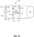
- FIG. 1A illustrates a clamp circuit 100 according to an embodiment.
- the clamp circuit 100 is configured to protect a load 101 against a current and/or voltage surge, which can be caused by lightning, for example.
- the load 101 can be, by example and not by limitation, an avionic system such as a flight control system, a flight recorder, a landing gear control system, and/or communications hardware.
- an avionic system such as a flight control system, a flight recorder, a landing gear control system, and/or communications hardware.
- the clamp circuit 100 can be used with loads other than the ones mentioned above and in applications other than avionics.
- a surge is modeled in FIG. 1A using a surge equivalent circuit 102 that includes a resistor 104 and a voltage source 106; the resistor 104 is used to model the impedance of the voltage source 106.
- the voltage source 106 can output a transient pulse having an amplitude of 600 V, and the pulse can last between about 5 and about 10 microseconds.
- the resistor 104 can be a 2 ⁇ resistor.
- Other surge events can be modeled using the equivalent circuit 102 by changing the pulse's duration and amplitude, as well as the impedance of the voltage source 106 (i.e. the resistor 104), without departing from the scope of the present disclosure.
- the clamp circuit 100 further includes a voltage source 108 that delivers power across the load 101.
- a voltage source 108 that delivers power across the load 101.
- the load 101 is connected across the positive terminal of the voltage source 108 and a ground terminal 103.
- the voltage source 108 can be a constant voltage source that outputs 28 V while delivering the required current drawn by the load 101.
- the clamp circuit 100 further includes a voltage sensitive device, namely a diode 110 that is reverse-biased and connected at its anode to a biasing circuit 116 of a power dissipation circuit 112.
- the diode 110 can be a Zener diode.
- the voltage sensitive device can be a metal oxide varistor (MOV) rather than a Zener diode.
- MOV metal oxide varistor
- a transient pulse having the characteristics described above is superimposed on the output voltage of the voltage source 108, causing the diode 110 to avalanche.
- the avalanche current flows to the biasing circuit 116 and activates the power dissipation circuit 112. Activation occurs by developing a turn on voltage, for the transistor 114 (e.g. a MOSFET), through a voltage divider formed by a resistor 118 and 120 within the biasing circuit 116.
- a voltage divider is formed between the pulse's source impedance (i.e. the resistor 104) and a resistor 122 disposed in series with the channel of the transistor 114.
- the resistor 122 serves as a dump resistor that holds the portion of the transient pulse seen by the load 101 to a low voltage.
- the transistor 114 acts in conjunction with the diode 110 and the biasing circuit 116, the voltage applied to the load 101 during the surge is held to the Zener diode voltage, added to a threshold voltage of the transistor 114.
- the Zener diode voltage of the diode 110 can be about 51 V and the threshold voltage of the transistor 114 can be about 3 V.
- the resistor 122 can be a metal element resistor.
- the power dissipation circuit can be implemented using other types of transistors.
- a clamp circuit 105 can be configured similarly to the clamp circuit 100, but with a power dissipation circuit that uses a Darlington pair formed by the bipolar junction transistors 115 and 117, instead of a MOSFET.
- the Darlington pair can provide more current drive than the MOSFET used in the clamp circuit 100, thus allowing the clamp circuit 105 to withstand higher surge currents.
- FIG. 2 illustrates a clamp circuit 200, according to another embodiment.
- a surge can be modeled using a surge equivalent circuit 202 similar to the equivalent circuit 102 shown in FIG. 1A .
- the clamp circuit 200 includes a voltage source 208 that delivers power across a load 201.
- the clamp circuit 200 further includes a diode 210, which is reverse-biased and connected at its anode to a biasing circuit 216 of a power dissipation circuit 212.
- the diode 210 can be a Zener diode.
- a transient pulse is superimposed on the output voltage of the voltage source 208, causing the diode 210 to avalanche.
- the avalanche current flows to the biasing circuit 216 and activates the power dissipation circuit 212.
- Activation occurs by developing a turn on voltage for a transistor 214 (e.g. a MOSFET) through a voltage divider formed by a resistor 218 and 220 within the biasing circuit 216.
- a transistor 214 e.g. a MOSFET
- the transistor 214 When the transistor 214 turns on, a voltage divider is formed between the pulse's source impedance (i.e. the resistor 204) and the channel of the transistor 214. As such, the transistor 214 can serve as a dump load that holds the portion of the transient pulse seen by the load 201 to a low voltage. That is, in the clamp circuit 200, the power of the surge is dissipated in transistor 214. This process acts in conjunction with the diode 210 and the biasing circuit 216 to limit the voltage applied to the load 201 during the surge. Specifically, the voltage across the load 201 is limited to the Zener diode voltage, added to a threshold voltage of the transistor 214. The Zener diode voltage of the diode 210 can be about 51 V, and the threshold voltage of the transistor 214 can be about 3 V. Thus, during a surge, the voltage across the load 201 is clamped to about 54 V.
- the clamp circuit 200 more of the surge pulse's energy or power is dissipated substantially in the transistor 214 rather than in the resistor 222.
- the diode 210 avalanches and the transistor 214 turns on, the voltage drop across the resistor 222 increases to hold the gate-to-source voltage (V GS ) of the transistor 214 at the threshold voltage of the transistor 214. Since the resistor 222 only has a voltage equal to V GS developed across it, it dissipates substantially less power than the resistor 122 of the clamp circuit 100.
- the clamp circuit 200 is advantageous for embodiments where the transistor 214 is implemented in semiconductor transistor technologies such as silicon carbide (SiC) and gallium nitride (GaN), which inherently provide higher temperature performance than silicon transistor technologies.
- semiconductor transistor technologies such as silicon carbide (SiC) and gallium nitride (GaN), which inherently provide higher temperature performance than silicon transistor technologies.
- the transistor 214 itself can be made to be the power dissipation element because it can inherently withstand higher temperatures caused by the power dissipation.
- SiC and GaN technologies provide transistors having faster switching times, which means that the clamp circuit 200 is advantageous for accommodating surge pulses that have a short duration.
- the clamp circuit 200 can have a sharp turn-on due the inherent fast switching times afforded by SiC or GaN transistors.
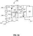
- FIG. 3A illustrates a clamp circuit 300, according to another embodiment.
- the clamp circuit 300 includes hardware configured for performing a built-in test (BIT) function, as shall be described in greater detail below.
- BIT built-in test
- a surge is modeled using a surge equivalent circuit 302 similar to the equivalent circuits 102 and 202, shown in FIGs. 1A , 1B , and 2 .
- the surge equivalent circuit 302 includes a voltage source 306 and a resistor 304.
- the clamp circuit 300 includes a voltage source 308 that delivers power across a load 301.
- the clamp circuit 300 further includes a diode 310, which is reverse-biased and connected at its anode to a biasing circuit 316 of a power dissipation circuit 312.
- the diode 310 can be a Zener diode.
- a transient pulse is superimposed on the output voltage of the voltage source 308, causing the diode 310 to avalanche.
- the avalanche current flows to the biasing circuit 316 and turns on the power dissipation circuit 312 by developing a turn on voltage for a transistor 314 (e.g. a MOSFET) through a voltage divider formed by a resistor 318 and 320 included in the biasing circuit 316.
- a transistor 314 e.g. a MOSFET
- a voltage divider is formed between the pulse's source impedance (i.e. the resistor 304) and a resistor 322 disposed in series with the channel of the transistor 314.
- the resistor 322 serves as a dump resistor holding the portion of the transient pulse seen by the load 301 to a low voltage. Because the transistor 314 acts in conjunction with the diode 310 and the biasing circuit 316, the voltage applied to the load 301 during the surge is held to the Zener diode voltage, added to a threshold voltage of the transistor 314.
- the Zener diode voltage of the diode 310 can be about 51 V and the threshold voltage of the transistor 314 can be about 3 V, which means that during a surge, the voltage across the load 301 is clamped to about 54 V. The power of the surge is thus dissipated in the resistor 322.
- the clamp circuit 300 further includes hardware configured for performing a BIT function, i.e. a self-test function capable of indicating whether or not the clamp circuit 300 is defective.
- a BIT function i.e. a self-test function capable of indicating whether or not the clamp circuit 300 is defective.
- the BIT function can test a functionality of the power dissipation circuit 312 of the clamp circuit 300.
- the BIT function provides the capability to assess whether the clamp circuit 300 is still functional.
- the BIT function can be performed at power up of one or more systems connected to the clamp circuit 300.
- the BIT function of the clamp circuit 300 can be performed by a sub-circuit 303 of the clamp circuit 300.
- the sub-circuit 303 can be implemented in the previously described clamp circuits 100 and 200 with a minimal increase in circuitry.
- the sub-circuit 303 includes a resistor 305, a transistor 307, a resistor 309, a resistor 319, a diode 311, and a driver 313.
- the sub-circuit 303 applies a test pulse to the gate of the transistor 314.
- the test pulse can be issued by a controller (not shown) at an input terminal 315 of the sub-circuit 303.
- the test pulse is buffered by the driver 313 and applied to the gate of the transistor 314 via the resistor 319.
- the transistor 307, the resistor 305, the transistor 309, the resistor 309, and the diode 311 serve as a readout circuit that is configured to output a BIT response signal at an output terminal 317 of the sub-circuit 303.
- the BIT response signal When the clamp circuit 300 is functional, i.e. when the power dissipation circuit 312 is functional, the BIT response signal is asserted as a replica of the test pulse signal inputted on the input terminal 315. However, when the clamp circuit 300 is not functional, i.e. when one or more components of the power dissipation circuit 312 is damaged, the BIT response signal is held at close to zero (or the ground 303). In other words, the BIT response signal at the output terminal 317 does not track the input test signal.
- the BIT function described above can be implemented with configurations other than the one shown in FIG. 3A .
- the BIT function can be implemented by asserting a test pulse at the cathode of the diode 310, as shown in FIG. 3B with respect to the clamp circuit 305.
- the test pulse can be issued by a controller (not shown) at the input terminal 315.
- the test pulse is buffered by the driver 313 and applied to at the cathode of the diode 310 via a path that includes the resistor 319, a diode 323, and a diode 321.
- the driver 313 applies a low current pulse at the cathode of the diode 310 to create a voltage greater than the Zener voltage to the diode 310, which initiates the test.
- the transistor 307, the resistor 305, the transistor 309, the resistor 309, and the diode 311 serve as a readout circuit configured to output a BIT response signal at the output terminal 317.
- the clamp circuit 305 can provide increased reliability in comparison with the clamp circuit 300. Specifically, because the test pulse propagates through more components of the circuit, there is a greater test coverage and more components can be tested.
- FIG. 4 illustrates a controller 400 (or a control system) for use in conjunction with the clamp circuit 300, or with the clamp circuits 100 and 200 suitably modified to include a BIT function.
- the controller 400 can interface with the clamp circuit 300 via a bi-directional bus 401 coupled to the input terminal 315 and to the output terminal 317, and to at least one other node of the clamp circuit 300 from which the controller 400 can monitor current or voltage.
- the controller 400 can be programmed to assert the BIT function test pulse and to receive the BIT function response signal.
- the controller 400 can include a processor 402 that has a specific structure.
- the specific structure can be imparted to the processor 402 by instructions stored in a memory 404 included therein and/or by instructions 420 that can be fetched by processor 412 from a storage medium 418.
- the storage medium 418 may be co-located with the controller 400 as shown, or it may be located elsewhere and be communicatively coupled to controller 400.
- the controller 400 can be a stand-alone programmable system, or it can be a programmable module located in a much larger system.
- the controller 400 can be part of an embedded-computer system configured to control and/or monitor one or more avionics systems included in an aircraft.
- the controller 400 may include one or more hardware and/or software components configured to fetch, decode, execute, store, analyze, distribute, evaluate, and/or categorize information.
- the controller 400 can include an input/output (I/O) module 414 that can be configured to interface with a one or more clamp circuits like the clamp circuit 300 via a bi-directional bus 401.
- I/O input/output
- the processor 402 may include one or more processing devices or cores (not shown). In some embodiments, the processor 402 may be a plurality of processors, each having either one or more cores.
- the processor 402 can be configured to execute instructions fetched from the memory 404, i.e. from one of memory blocks 412, 410, 408, or 406, or the instructions may be fetched from the storage medium 418, or from a remote device connected to the controller 400 via a communication interface 416.
- the storage medium 418 and/or memory 404 may include a volatile or non-volatile, magnetic, semiconductor, tape, optical, removable, non-removable, read-only, random-access, or any type of non-transitory computer-readable computer medium.
- the storage medium 418 and/or the memory 404 may include programs and/or other information that may be used by the processor 402.
- the storage medium 418 may be configured to log data processed, recorded, or collected during the operation of controller 400. The data may be time-stamped, location-stamped, cataloged, indexed, or organized in a variety of ways consistent with data storage practice.
- the memory block 406 may be a BIT module, and it may include instructions that, when executed by the processor 402, cause the processor 402 to perform certain operations.
- the operations can include receiving a signal indicating that a clamp circuit connected to the controller 400 has been powered up. Receiving such a signal can be performed by monitoring a status of the clamp circuit via the bus 401.
- Power up can include, for example, switching on the voltage source 308 in the clamp circuit 300 to deliver power across the load 301.
- the controller 400 Upon receiving the confirmation of power up, the controller 400 can initiate a built-in-test (BIT) sequence.
- BIT built-in-test
- the BIT sequence can include asserting a test pulse signal on the input terminal of the BIT function sub-circuit of the clamp circuit.
- the BIT sequence can include receiving a BIT function response signal from the output terminal of the BIT function sub-circuit.
- the BIT sequence can further include classifying the BIT response signal to indicate whether or not the clamp circuit is functional. For example, classification can include comparing the BIT response signal with the BIT test signal and indicating based on the comparison whether the BIT function of the clamp circuit is operational.
- the controller 400 can indicate that the BIT function of the clamp circuit is not damaged when a digital "1" is obtained from performing a logical "AND” operation between the BIT test signal and the BIT response signal and that the clamp circuit is damaged when the operation yields a digital "0.”
- Other classifying means that are readily evident to one of skill in the art can also be used, without departing from the scope of the present disclosure.
- the method 500 can be executed by a controller like the controller 400, and it can begin at a block 502 in FIG. 5 .
- the method 500 can include receiving power up information from a clamp circuit coupled to the controller 400.
- the power up information can be a signal that indicates when (or whether or not) power has been turned on across a load connected to the clamp circuit.
- the method 500 can include asserting a BIT test signal at an input terminal of a BIT function sub-circuit of the clamp circuit.
- the BIT test signal can be a digital pulse.
- the method 500 can then include receiving a BIT response signal (at block 508) in response to the BIT test signal having been asserted.
- the BIT response signal can be received by the controller 400 from an output terminal of the clamp circuit.
- the method 500 can include de-asserting the BIT test signal (block 510) and classifying the BIT response signal (block 512). Classification can be performed in order to determine whether the clamp circuit is functional, i.e. whether it can protect the load from an eventual surge. Upon classification, the method 500 can include reporting the result of the classification to indicate whether the clamp circuit is functional (block 514), at which point, if the clamp circuit is reported as being not functional, remedial action can be taken. The method 500 can then end at block 516.
- the embodiments have been described in the context of avionics and avionics systems, one of skill in the art will readily recognize that the embodiments generally apply to applications in which protection against surges is required.
- the embodiments can be used to protect telecommunications or RF broadcasting equipment.
- the method 500 can be used to periodically or continually check whether a clamp circuit is functional and is not limited to checking functionality solely at power up.
- the exemplary clamp circuits shown one of ordinary skill in the art will readily appreciate that other arrangements of components and/or other types of components can be used without departing from the scope of the present disclosure.
- either p or n MOSFETS can be used or either n-p-n or p-n-p bipolar transistors can be used.
- IGBTS or power MOSFETS can be used to implement the clamp circuits and systems described herein.
Landscapes
- Electronic Switches (AREA)
Abstract
Description
- The present invention relates generally to circuit protection. In particular, the present invention relates to providing enhanced transient protection circuits.
- Lightning protection for avionics systems is typically provided by protection circuits that use transorbs or similar clamping devices. These protection circuits are typically designed to dissipate large amounts of energy but often at the expense of device precision. For example, the operating voltage of most transorbs vary significantly from part to part, as well as with operating current and temperature. Therefore, fitting these protection circuits in avionics systems is technologically challenging and economically prohibitive because the protection circuits must be custom-designed for each system due to the variability in component characteristics and performance.
- Furthermore, transorbs cannot be readily tested once they are embedded and in use in a lightning protection circuit. Consequently, a load coupled to the circuit may remain unprotected, because it is not possible to know whether a transorb has failed. Stated otherwise and more generally, in typical lightning protection circuits that use transorbs, it is challenging to ascertain whether a load is actually being protected because it is difficult to determine whether the transorbs are operational when the circuits are powered on.
- The examples featured herein help solve or mitigate the above noted issues as well as other issues known in the art. For example, by taking advantage of newly improved transistor devices using silicon, silicon carbide, or gallium nitride semiconductors, some of the embodiments provide transient protection circuits that have precise operational characteristics as well as built-in test functions for determining whether the surge protection elements of the circuits are operational.
- More specifically, some examples provide transient lightning protection circuits having clamping voltages that are more tightly controlled because they include signal level voltage-sensitive elements that have improved component characteristics and performance with respect to typical transorbs. Moreover, some of the examples provide the capability to continually or periodically assess the functionality of a protection circuit.
- Under certain circumstances, an example provides a clamp circuit for protecting a load against a surge voltage. The clamp circuit includes a power dissipation circuit that includes at least one transistor and a resistor. The clamp circuit further includes a voltage sensitive device configured to turn the at least one transistor on when a surge occurs. The power dissipation circuit is thus configurable to turn on the transistor to dissipate power from the surge across one of the resistor and the at least one transistor.
- Another example provides a clamp circuit for protecting a load against a surge. The clamp circuit includes a power dissipation circuit that includes at least one transistor and a resistor. The power dissipation circuit is configurable to dissipate power from the surge by turning on the at least one transistor. The clamp circuit further includes a sub-circuit configured to test a functionality of the power dissipation circuit.
- Additional features, modes of operations, advantages, and other aspects of various examples are described below with reference to the accompanying drawings. It is noted that the present disclosure is not limited to the specific examples described herein. These embodiments are presented for illustrative purposes, and additional examples, or modifications of the examples disclosed, will be readily apparent to persons skilled in the relevant art(s) based on the teachings provided.
- The illustrative embodiments may take form in various components and arrangements of components. The illustrative embodiments are shown in the accompanying drawings, throughout which like reference numerals may indicate corresponding or similar parts in the various drawings. The drawings are for purposes of illustrating the embodiments and are not to be construed as limiting the disclosure. Given the following enabling description of the drawings, the novel aspects of the present disclosure should become evident to a person of ordinary skill in the relevant art(s).
-
FIG. 1A illustrates an exemplary clamp circuit in accordance with various aspects described herein. -
FIG. 1B illustrates an exemplary clamp circuit in accordance with various aspects described herein. -
FIG. 2 illustrates an exemplary clamp circuit in accordance with various aspects described herein. -
FIG. 3A illustrates an exemplary clamp circuit in accordance with various aspects described herein. -
FIG. 3B illustrates an exemplary clamp circuit in accordance with various aspects described herein. -
FIG. 4 illustrates an exemplary system in accordance with various aspects described herein. -
FIG. 5 illustrates a flow chart of an exemplary method in accordance with various aspects described herein. - While the illustrative embodiments are described herein for particular applications, it should be understood that the present disclosure is not limited thereto. Those skilled in the art and with access to the teachings provided herein will recognize additional applications, modifications, and embodiments within the scope thereof and additional fields in which the present disclosure would be of significant utility.
-
FIG. 1A illustrates aclamp circuit 100 according to an embodiment. Theclamp circuit 100 is configured to protect aload 101 against a current and/or voltage surge, which can be caused by lightning, for example. Theload 101 can be, by example and not by limitation, an avionic system such as a flight control system, a flight recorder, a landing gear control system, and/or communications hardware. One of ordinary skill in the art will readily understand that theclamp circuit 100 can be used with loads other than the ones mentioned above and in applications other than avionics. - To better describe the operation of the
clamp circuit 100, a surge is modeled inFIG. 1A using a surgeequivalent circuit 102 that includes aresistor 104 and avoltage source 106; theresistor 104 is used to model the impedance of thevoltage source 106. When the surge is due to lightning, thevoltage source 106 can output a transient pulse having an amplitude of 600 V, and the pulse can last between about 5 and about 10 microseconds. Moreover, theresistor 104 can be a 2 □ resistor. Other surge events can be modeled using theequivalent circuit 102 by changing the pulse's duration and amplitude, as well as the impedance of the voltage source 106 (i.e. the resistor 104), without departing from the scope of the present disclosure. - The
clamp circuit 100 further includes avoltage source 108 that delivers power across theload 101. In the absence of a surge (i.e. when thevoltage source 106 has zero amplitude and theresistor 104 is zero □), theload 101 is connected across the positive terminal of thevoltage source 108 and aground terminal 103. In one embodiment, thevoltage source 108 can be a constant voltage source that outputs 28 V while delivering the required current drawn by theload 101. - The
clamp circuit 100 further includes a voltage sensitive device, namely a diode 110 that is reverse-biased and connected at its anode to abiasing circuit 116 of apower dissipation circuit 112. The diode 110 can be a Zener diode. In some embodiments of theclamp circuit 100, as well as in alternate embodiments of the exemplary clamp circuits described hereinafter, the voltage sensitive device can be a metal oxide varistor (MOV) rather than a Zener diode. These embodiments are advantageous when thetransistor 114 is implemented using a bipolar transistor or is substituted for a Darlington pair; the MOV can provide improved performance because its relatively higher power density can be leveraged for accommodating the higher drive currents required by the bipolar transistor or the Darlington pair. - When a surge occurs, a transient pulse having the characteristics described above is superimposed on the output voltage of the
voltage source 108, causing the diode 110 to avalanche. The avalanche current flows to thebiasing circuit 116 and activates thepower dissipation circuit 112. Activation occurs by developing a turn on voltage, for the transistor 114 (e.g. a MOSFET), through a voltage divider formed by aresistor circuit 116. - As the
transistor 114 turns on, a voltage divider is formed between the pulse's source impedance (i.e. the resistor 104) and aresistor 122 disposed in series with the channel of thetransistor 114. As such, theresistor 122 serves as a dump resistor that holds the portion of the transient pulse seen by theload 101 to a low voltage. Specifically, because thetransistor 114 acts in conjunction with the diode 110 and thebiasing circuit 116, the voltage applied to theload 101 during the surge is held to the Zener diode voltage, added to a threshold voltage of thetransistor 114. In some embodiments, the Zener diode voltage of the diode 110 can be about 51 V and the threshold voltage of thetransistor 114 can be about 3 V. Thus, during a surge, the voltage across theload 101 is limited, i.e. clamped, to about 54 V. The power of the surge is thus dissipated substantially in theresistor 122. In some embodiments, theresistor 122 can be a metal element resistor. - In alternate embodiments, the power dissipation circuit can be implemented using other types of transistors. For example, as shown in
FIG. 1B , aclamp circuit 105 can be configured similarly to theclamp circuit 100, but with a power dissipation circuit that uses a Darlington pair formed by thebipolar junction transistors clamp circuit 100, thus allowing theclamp circuit 105 to withstand higher surge currents. -
FIG. 2 illustrates aclamp circuit 200, according to another embodiment. In theclamp circuit 200, a surge can be modeled using a surgeequivalent circuit 202 similar to theequivalent circuit 102 shown inFIG. 1A . Theclamp circuit 200 includes avoltage source 208 that delivers power across aload 201. Theclamp circuit 200 further includes adiode 210, which is reverse-biased and connected at its anode to abiasing circuit 216 of apower dissipation circuit 212. - The
diode 210 can be a Zener diode. When the surge occurs, a transient pulse is superimposed on the output voltage of thevoltage source 208, causing thediode 210 to avalanche. The avalanche current flows to thebiasing circuit 216 and activates thepower dissipation circuit 212. Activation occurs by developing a turn on voltage for a transistor 214 (e.g. a MOSFET) through a voltage divider formed by aresistor circuit 216. - When the
transistor 214 turns on, a voltage divider is formed between the pulse's source impedance (i.e. the resistor 204) and the channel of thetransistor 214. As such, thetransistor 214 can serve as a dump load that holds the portion of the transient pulse seen by theload 201 to a low voltage. That is, in theclamp circuit 200, the power of the surge is dissipated intransistor 214. This process acts in conjunction with thediode 210 and thebiasing circuit 216 to limit the voltage applied to theload 201 during the surge. Specifically, the voltage across theload 201 is limited to the Zener diode voltage, added to a threshold voltage of thetransistor 214. The Zener diode voltage of thediode 210 can be about 51 V, and the threshold voltage of thetransistor 214 can be about 3 V. Thus, during a surge, the voltage across theload 201 is clamped to about 54 V. - In the
clamp circuit 200, more of the surge pulse's energy or power is dissipated substantially in thetransistor 214 rather than in theresistor 222. When thediode 210 avalanches and thetransistor 214 turns on, the voltage drop across theresistor 222 increases to hold the gate-to-source voltage (VGS) of thetransistor 214 at the threshold voltage of thetransistor 214. Since theresistor 222 only has a voltage equal to VGS developed across it, it dissipates substantially less power than theresistor 122 of theclamp circuit 100. - Accordingly, nearly all the energy of the surge is dissipated in the
transistor 214. Theclamp circuit 200 is advantageous for embodiments where thetransistor 214 is implemented in semiconductor transistor technologies such as silicon carbide (SiC) and gallium nitride (GaN), which inherently provide higher temperature performance than silicon transistor technologies. - Specifically, when either a SiC or a GaN transistor is used, the
transistor 214 itself can be made to be the power dissipation element because it can inherently withstand higher temperatures caused by the power dissipation. Moreover, SiC and GaN technologies provide transistors having faster switching times, which means that theclamp circuit 200 is advantageous for accommodating surge pulses that have a short duration. In addition, theclamp circuit 200 can have a sharp turn-on due the inherent fast switching times afforded by SiC or GaN transistors. -
FIG. 3A illustrates aclamp circuit 300, according to another embodiment. Theclamp circuit 300 includes hardware configured for performing a built-in test (BIT) function, as shall be described in greater detail below. In theclamp circuit 300, a surge is modeled using a surgeequivalent circuit 302 similar to theequivalent circuits FIGs. 1A ,1B , and2 . The surgeequivalent circuit 302 includes avoltage source 306 and aresistor 304. - The
clamp circuit 300 includes avoltage source 308 that delivers power across aload 301. Theclamp circuit 300 further includes adiode 310, which is reverse-biased and connected at its anode to abiasing circuit 316 of apower dissipation circuit 312. Thediode 310 can be a Zener diode. When the surge occurs, a transient pulse is superimposed on the output voltage of thevoltage source 308, causing thediode 310 to avalanche. The avalanche current flows to thebiasing circuit 316 and turns on thepower dissipation circuit 312 by developing a turn on voltage for a transistor 314 (e.g. a MOSFET) through a voltage divider formed by aresistor biasing circuit 316. - When the
transistor 314 turns on, a voltage divider is formed between the pulse's source impedance (i.e. the resistor 304) and aresistor 322 disposed in series with the channel of thetransistor 314. As such, theresistor 322 serves as a dump resistor holding the portion of the transient pulse seen by theload 301 to a low voltage. Because thetransistor 314 acts in conjunction with thediode 310 and thebiasing circuit 316, the voltage applied to theload 301 during the surge is held to the Zener diode voltage, added to a threshold voltage of thetransistor 314. - In some embodiments, the Zener diode voltage of the
diode 310 can be about 51 V and the threshold voltage of thetransistor 314 can be about 3 V, which means that during a surge, the voltage across theload 301 is clamped to about 54 V. The power of the surge is thus dissipated in theresistor 322. - The
clamp circuit 300 further includes hardware configured for performing a BIT function, i.e. a self-test function capable of indicating whether or not theclamp circuit 300 is defective. Generally, the BIT function can test a functionality of thepower dissipation circuit 312 of theclamp circuit 300. - For example, depending on a surge's magnitude and/or on the frequency of surges, components of the
power dissipation circuit 312 can be damaged, and theclamp circuit 300 can cease to protect theload 301 against subsequent surges. As such, the BIT function provides the capability to assess whether theclamp circuit 300 is still functional. In an avionics setting, the BIT function can be performed at power up of one or more systems connected to theclamp circuit 300. - The BIT function of the
clamp circuit 300 can be performed by asub-circuit 303 of theclamp circuit 300. The sub-circuit 303 can be implemented in the previously describedclamp circuits resistor 305, atransistor 307, aresistor 309, aresistor 319, adiode 311, and adriver 313. - The sub-circuit 303 applies a test pulse to the gate of the
transistor 314. The test pulse can be issued by a controller (not shown) at aninput terminal 315 of the sub-circuit 303. The test pulse is buffered by thedriver 313 and applied to the gate of thetransistor 314 via theresistor 319. Thetransistor 307, theresistor 305, thetransistor 309, theresistor 309, and thediode 311 serve as a readout circuit that is configured to output a BIT response signal at anoutput terminal 317 of the sub-circuit 303. - When the
clamp circuit 300 is functional, i.e. when thepower dissipation circuit 312 is functional, the BIT response signal is asserted as a replica of the test pulse signal inputted on theinput terminal 315. However, when theclamp circuit 300 is not functional, i.e. when one or more components of thepower dissipation circuit 312 is damaged, the BIT response signal is held at close to zero (or the ground 303). In other words, the BIT response signal at theoutput terminal 317 does not track the input test signal. - One of skill in the art will readily understand that the BIT function described above can be implemented with configurations other than the one shown in
FIG. 3A . For example, in an alternate configuration, the BIT function can be implemented by asserting a test pulse at the cathode of thediode 310, as shown inFIG. 3B with respect to theclamp circuit 305. - As in the
clamp circuit 300, in theclamp circuit 305, the test pulse can be issued by a controller (not shown) at theinput terminal 315. The test pulse is buffered by thedriver 313 and applied to at the cathode of thediode 310 via a path that includes theresistor 319, adiode 323, and adiode 321. Thedriver 313 applies a low current pulse at the cathode of thediode 310 to create a voltage greater than the Zener voltage to thediode 310, which initiates the test. Thetransistor 307, theresistor 305, thetransistor 309, theresistor 309, and thediode 311 serve as a readout circuit configured to output a BIT response signal at theoutput terminal 317. - The
clamp circuit 305 can provide increased reliability in comparison with theclamp circuit 300. Specifically, because the test pulse propagates through more components of the circuit, there is a greater test coverage and more components can be tested. -
FIG. 4 illustrates a controller 400 (or a control system) for use in conjunction with theclamp circuit 300, or with theclamp circuits controller 400 can interface with theclamp circuit 300 via abi-directional bus 401 coupled to theinput terminal 315 and to theoutput terminal 317, and to at least one other node of theclamp circuit 300 from which thecontroller 400 can monitor current or voltage. Specifically, thecontroller 400 can be programmed to assert the BIT function test pulse and to receive the BIT function response signal. - The
controller 400 can include aprocessor 402 that has a specific structure. The specific structure can be imparted to theprocessor 402 by instructions stored in amemory 404 included therein and/or byinstructions 420 that can be fetched byprocessor 412 from astorage medium 418. Thestorage medium 418 may be co-located with thecontroller 400 as shown, or it may be located elsewhere and be communicatively coupled tocontroller 400. - The
controller 400 can be a stand-alone programmable system, or it can be a programmable module located in a much larger system. For example, thecontroller 400 can be part of an embedded-computer system configured to control and/or monitor one or more avionics systems included in an aircraft. Thecontroller 400 may include one or more hardware and/or software components configured to fetch, decode, execute, store, analyze, distribute, evaluate, and/or categorize information. Furthermore, thecontroller 400 can include an input/output (I/O)module 414 that can be configured to interface with a one or more clamp circuits like theclamp circuit 300 via abi-directional bus 401. - The
processor 402 may include one or more processing devices or cores (not shown). In some embodiments, theprocessor 402 may be a plurality of processors, each having either one or more cores. Theprocessor 402 can be configured to execute instructions fetched from thememory 404, i.e. from one of memory blocks 412, 410, 408, or 406, or the instructions may be fetched from thestorage medium 418, or from a remote device connected to thecontroller 400 via acommunication interface 416. - Furthermore, without loss of generality, the
storage medium 418 and/ormemory 404 may include a volatile or non-volatile, magnetic, semiconductor, tape, optical, removable, non-removable, read-only, random-access, or any type of non-transitory computer-readable computer medium. Thestorage medium 418 and/or thememory 404 may include programs and/or other information that may be used by theprocessor 402. Furthermore, thestorage medium 418 may be configured to log data processed, recorded, or collected during the operation ofcontroller 400. The data may be time-stamped, location-stamped, cataloged, indexed, or organized in a variety of ways consistent with data storage practice. - In one embodiment, for example, the
memory block 406 may be a BIT module, and it may include instructions that, when executed by theprocessor 402, cause theprocessor 402 to perform certain operations. The operations can include receiving a signal indicating that a clamp circuit connected to thecontroller 400 has been powered up. Receiving such a signal can be performed by monitoring a status of the clamp circuit via thebus 401. Power up can include, for example, switching on thevoltage source 308 in theclamp circuit 300 to deliver power across theload 301. Upon receiving the confirmation of power up, thecontroller 400 can initiate a built-in-test (BIT) sequence. - The BIT sequence can include asserting a test pulse signal on the input terminal of the BIT function sub-circuit of the clamp circuit. The BIT sequence can include receiving a BIT function response signal from the output terminal of the BIT function sub-circuit. The BIT sequence can further include classifying the BIT response signal to indicate whether or not the clamp circuit is functional. For example, classification can include comparing the BIT response signal with the BIT test signal and indicating based on the comparison whether the BIT function of the clamp circuit is operational.
- In one example, the
controller 400 can indicate that the BIT function of the clamp circuit is not damaged when a digital "1" is obtained from performing a logical "AND" operation between the BIT test signal and the BIT response signal and that the clamp circuit is damaged when the operation yields a digital "0." Other classifying means that are readily evident to one of skill in the art can also be used, without departing from the scope of the present disclosure. - Having set forth various exemplary embodiments, a
method 500 consistent with their operation is now described with respect toFIG. 5 . Themethod 500 can be executed by a controller like thecontroller 400, and it can begin at ablock 502 inFIG. 5 . Atblock 504, themethod 500 can include receiving power up information from a clamp circuit coupled to thecontroller 400. The power up information can be a signal that indicates when (or whether or not) power has been turned on across a load connected to the clamp circuit. - Upon receiving the power up information, at
block 506, and in response to power having been turned on across the load, themethod 500 can include asserting a BIT test signal at an input terminal of a BIT function sub-circuit of the clamp circuit. For example and not by limitation, the BIT test signal can be a digital pulse. Themethod 500 can then include receiving a BIT response signal (at block 508) in response to the BIT test signal having been asserted. The BIT response signal can be received by thecontroller 400 from an output terminal of the clamp circuit. - Once the BIT response signal is received, the
method 500 can include de-asserting the BIT test signal (block 510) and classifying the BIT response signal (block 512). Classification can be performed in order to determine whether the clamp circuit is functional, i.e. whether it can protect the load from an eventual surge. Upon classification, themethod 500 can include reporting the result of the classification to indicate whether the clamp circuit is functional (block 514), at which point, if the clamp circuit is reported as being not functional, remedial action can be taken. Themethod 500 can then end atblock 516. - While the embodiments have been described in the context of avionics and avionics systems, one of skill in the art will readily recognize that the embodiments generally apply to applications in which protection against surges is required. For example, the embodiments can be used to protect telecommunications or RF broadcasting equipment. Moreover, the
method 500 can be used to periodically or continually check whether a clamp circuit is functional and is not limited to checking functionality solely at power up. Furthermore, with respect to the exemplary clamp circuits shown, one of ordinary skill in the art will readily appreciate that other arrangements of components and/or other types of components can be used without departing from the scope of the present disclosure. For example, either p or n MOSFETS can be used or either n-p-n or p-n-p bipolar transistors can be used. Moreover, instead of MOSFETs, IGBTS or power MOSFETS can be used to implement the clamp circuits and systems described herein. - Those skilled in the relevant art(s) will appreciate that various adaptations and modifications of the embodiments described above can be configured without departing from the scope of the disclosure. Therefore, it is to be understood that, within the scope of the appended claims, the disclosure may be practiced other than as specifically described herein.
- Various aspects and embodiments of the present invention are defined by the following numbered clauses:
- 1. A clamp circuit for protecting a load against a surge, the clamp circuit comprising:
- a power dissipation circuit including at least one transistor and a resistor;
- a voltage sensitive device configured to limit a voltage across the load when the surge occurs;
- wherein the power dissipation circuit is configured to turn on the at least one transistor to dissipate power generated by the surge across one of the resistor and the at least one transistor.
- 2. The clamp circuit according to clause 1, wherein the voltage sensitive device is one of a Zener diode and a metal oxide varistor (MOV).
- 3. The clamp circuit according to any preceding clause, wherein the at least one transistor is selected from the group consisting of a metal-oxide semiconductor field-effect transistor (MOSFET), a bipolar junction transistor (BT), and a Darlington pair.
- 4. The clamp circuit according to any preceding clause, wherein the MOSFET is one of a Gallium Nitride MOSFET and a Silicon Carbide MOSFET.
- 5. The clamp circuit according to any preceding clause, wherein the resistor is disposed at one of the source and the drain of the at least one transistor.
- 6. The clamp circuit according to any preceding clause, wherein the at least one transistor is an insulated-gate bipolar transistor (IGBT).
- 7. The clamp circuit according to any preceding clause, wherein the resistor is a metal element resistor.
- 8. The clamp circuit according to any preceding clause, wherein the Zener diode is configured to avalanche in response to the surge occurring.
- 9. The clamp circuit according to any preceding clause, wherein the load is an avionics system.
- 10. The clamp circuit according to any preceding clause, further comprising a sub-circuit configured to perform a built-in test function.
- 11. A clamp circuit for protecting a load against a surge, the clamp circuit comprising:
- a power dissipation circuit including at least one transistor and a resistor, wherein the power dissipation circuit is configured to dissipate power from the surge across one of the resistor and the at least one transistor by turning on the at least one transistor; and
- a sub-circuit configured to test a functionality of the power dissipation circuit.
- 12. The clamp circuit according to any preceding clause, wherein sub-circuit includes a terminal configured to receive an input signal for activating the sub-circuit.
- 13. The clamp circuit according to any preceding clause, wherein the sub-circuit includes an output terminal configured to output signal indicative of the viability of the power-dissipation circuit.
- 14. The clamp circuit according to any preceding clause, wherein the sub-circuit includes a readout circuit configured to indicate whether the at least one transistor or the resistor is damaged.
- 15. The clamp circuit according to any preceding clause, wherein the load is an avionics system.
- 16. A method for operating a clamp circuit configured to protect a load against a surge, the method comprising:
- powering the clamp circuit;
- enabling a built-in test function of the clamp circuit; and
- determining, in response to enabling the built-in test function, a status of the clamp circuit.
- 17. The method according to any preceding clause, wherein enabling the built-in test function includes asserting a digital signal at an input terminal of the clamp circuit.
- 18. The method according to any preceding clause, wherein determining the status includes asserting a digital signal at an output terminal of the clamp circuit, wherein the digital signal is indicative of whether a power dissipation circuit included in the clamp circuit is functional.
- 19. The method according to any preceding clause, wherein the load is an avionics system.
- 20. The method according to any preceding clause, wherein the surge occurs in response to lightning.
Claims (15)
- A clamp circuit (100) for protecting a load (101) against a surge, the clamp circuit (100) comprising:a power dissipation circuit (112) including at least one transistor (114) and a resistor (122);a voltage sensitive device (110) configured to limit a voltage across the load (101) when the surge occurs;wherein the power dissipation circuit (112) is configured to turn on the at least one transistor (114) to dissipate power generated by the surge across one of the resistor (122) and the at least one transistor (114).
- The clamp circuit (100) according to claim 1, wherein the voltage sensitive device (110) is one of a Zener diode and a metal oxide varistor (MOV).
- The clamp circuit (100) according to either of claim 1 or 2, wherein the at least one transistor (114) is selected from the group consisting of a metal-oxide semiconductor field-effect transistor (MOSFET), a bipolar junction transistor (BT), and a Darlington pair.
- The clamp circuit (100) according to claim 3, wherein the MOSFET is one of a Gallium Nitride MOSFET and a Silicon Carbide MOSFET.
- The clamp circuit (100) according to any preceding claim, wherein the resistor (122) is disposed at one of the source and the drain of the at least one transistor (114).
- The clamp circuit (100) according to any preceding claim, wherein the at least one transistor (114) is an insulated-gate bipolar transistor (IGBT).
- The clamp circuit (100) according to any preceding claim, wherein the resistor (122) is a metal element resistor (122).
- The clamp circuit (100) according to claim 2 or any claim dependent thereon, wherein the Zener diode is configured to avalanche in response to the surge occurring.
- The clamp circuit (100) according to any preceding claim, wherein the load (101) is an avionics system.
- The clamp circuit (100, 300) according to any preceding claim, further comprising a sub-circuit (303) configured to perform a built-in test function.
- A method for operating a clamp circuit (100) configured to protect a load (101) against a surge, the method comprising:powering the clamp circuit (100);enabling a built-in test function of the clamp circuit; anddetermining, in response to enabling the built-in test function, a status of the clamp circuit.
- The method according to claim 11, wherein enabling the built-in test function includes asserting a digital signal at an input terminal of the clamp circuit (100).
- The method according to either of claim 11 or 12, wherein determining the status includes asserting a digital signal at an output terminal of the clamp circuit (100), wherein the digital signal is indicative of whether a power dissipation circuit included in the clamp circuit is functional.
- The method according to any of claims 11 to 13, wherein the load (101) is an avionics system.
- The method according to any of claims 11 to 14, wherein the surge occurs in response to lightning.
Applications Claiming Priority (1)
| Application Number | Priority Date | Filing Date | Title |
|---|---|---|---|
| US15/243,526 US10431974B2 (en) | 2016-08-22 | 2016-08-22 | Surge protection circuit |
Publications (2)
| Publication Number | Publication Date |
|---|---|
| EP3288137A1 true EP3288137A1 (en) | 2018-02-28 |
| EP3288137B1 EP3288137B1 (en) | 2025-09-24 |
Family
ID=59677060
Family Applications (1)
| Application Number | Title | Priority Date | Filing Date |
|---|---|---|---|
| EP17186421.8A Active EP3288137B1 (en) | 2016-08-22 | 2017-08-16 | Surge protection circuit |
Country Status (4)
| Country | Link |
|---|---|
| US (2) | US10431974B2 (en) |
| EP (1) | EP3288137B1 (en) |
| BR (1) | BR102017017644A2 (en) |
| CA (1) | CA2975741C (en) |
Cited By (1)
| Publication number | Priority date | Publication date | Assignee | Title |
|---|---|---|---|---|
| EP3614516A1 (en) * | 2018-08-20 | 2020-02-26 | Hamilton Sundstrand Corporation | Using aircraft electric icing protection system for electrical power system quality |
Families Citing this family (5)
| Publication number | Priority date | Publication date | Assignee | Title |
|---|---|---|---|---|
| US10431974B2 (en) | 2016-08-22 | 2019-10-01 | Ge Aviation Systems, Llc | Surge protection circuit |
| JP2022526534A (en) * | 2019-03-28 | 2022-05-25 | シグニファイ ホールディング ビー ヴィ | Avalanche Trigger Overvoltage Protection |
| EP4213327A1 (en) * | 2022-01-14 | 2023-07-19 | ADB Safegate BV | Voltage limiting device for constant current circuits |
| US12597853B2 (en) * | 2022-11-17 | 2026-04-07 | Hdm Systems Corporation | Input transient protection and reverse protection for inverters |
| US20240339827A1 (en) * | 2023-04-04 | 2024-10-10 | Timothy A Carty | System and method for suppressing electromagnetic pulse-induced electrical system surges |
Citations (5)
| Publication number | Priority date | Publication date | Assignee | Title |
|---|---|---|---|---|
| US4849845A (en) * | 1988-10-24 | 1989-07-18 | Sundstrand Corporation | Transient suppressor |
| US20110188162A1 (en) * | 2010-02-01 | 2011-08-04 | Phoenix Contact Gmbh & Co. Kg | Device for diverting surge currents or transient overvoltages |
| DE202012012874U1 (en) * | 2012-12-06 | 2014-02-11 | Deutsches Zentrum für Luft- und Raumfahrt e.V. | Protective device for protecting at least one electrical load from voltage overshoots |
| EP2701256A1 (en) * | 2012-08-22 | 2014-02-26 | Raycap Corporation | Devices and methods for overvoltage protection |
| US20140340799A1 (en) * | 2013-05-15 | 2014-11-20 | Oeco, Llc | Active transient voltage suppression device |
Family Cites Families (15)
| Publication number | Priority date | Publication date | Assignee | Title |
|---|---|---|---|---|
| JPH0697739B2 (en) * | 1989-12-21 | 1994-11-30 | 株式会社東芝 | Overvoltage protection circuit |
| US6792306B2 (en) * | 2000-03-10 | 2004-09-14 | Biophoretic Therapeutic Systems, Llc | Finger-mounted electrokinetic delivery system for self-administration of medicaments and methods therefor |
| TW517422B (en) * | 2001-05-18 | 2003-01-11 | Palmax Technology Co Ltd | Input protection circuit of hand-held electrical apparatus |
| US7706112B2 (en) | 2006-12-19 | 2010-04-27 | Akros Silicon Inc. | Active clamp protection device |
| US8598899B2 (en) * | 2011-01-25 | 2013-12-03 | Hamilton Sundstrand Corporation | Built-in test for an overvoltage protection circuit |
| DE102011012284A1 (en) * | 2011-02-24 | 2012-08-30 | Knorr-Bremse Systeme für Nutzfahrzeuge GmbH | Overvoltage protection circuit and method for checking an overvoltage protection circuit |
| AU2013216713A1 (en) * | 2012-02-10 | 2014-08-14 | Transtector Systems, Inc. | Transient control technology circuit |
| CN103296664A (en) * | 2012-03-02 | 2013-09-11 | 鸿富锦精密工业(深圳)有限公司 | Overvoltage protection circuit and electronic device with overvoltage protection circuit |
| CN202524075U (en) | 2012-04-11 | 2012-11-07 | 上海尊瑞电子有限公司 | Direct-current surge protection module |
| GB2501105A (en) * | 2012-04-12 | 2013-10-16 | Eltek As | AC-DC converter overvoltage protection circuit |
| US9013848B2 (en) * | 2012-09-27 | 2015-04-21 | Alpha And Omega Semiconductor Incorporated | Active clamp protection circuit for power semiconductor device for high frequency switching |
| US9071245B2 (en) * | 2013-04-24 | 2015-06-30 | Hamilton Sundstrand Corporation | Solid state power controller gate control |
| US9076656B2 (en) * | 2013-05-02 | 2015-07-07 | Freescale Semiconductor, Inc. | Electrostatic discharge (ESD) clamp circuit with high effective holding voltage |
| US9960588B2 (en) * | 2015-03-19 | 2018-05-01 | Infineon Technologies Ag | Power switch device |
| US10431974B2 (en) | 2016-08-22 | 2019-10-01 | Ge Aviation Systems, Llc | Surge protection circuit |
-
2016
- 2016-08-22 US US15/243,526 patent/US10431974B2/en active Active
-
2017
- 2017-08-10 CA CA2975741A patent/CA2975741C/en not_active Expired - Fee Related
- 2017-08-16 EP EP17186421.8A patent/EP3288137B1/en active Active
- 2017-08-17 BR BR102017017644-4A patent/BR102017017644A2/en not_active IP Right Cessation
-
2019
- 2019-09-20 US US16/577,300 patent/US11381077B2/en active Active
Patent Citations (5)
| Publication number | Priority date | Publication date | Assignee | Title |
|---|---|---|---|---|
| US4849845A (en) * | 1988-10-24 | 1989-07-18 | Sundstrand Corporation | Transient suppressor |
| US20110188162A1 (en) * | 2010-02-01 | 2011-08-04 | Phoenix Contact Gmbh & Co. Kg | Device for diverting surge currents or transient overvoltages |
| EP2701256A1 (en) * | 2012-08-22 | 2014-02-26 | Raycap Corporation | Devices and methods for overvoltage protection |
| DE202012012874U1 (en) * | 2012-12-06 | 2014-02-11 | Deutsches Zentrum für Luft- und Raumfahrt e.V. | Protective device for protecting at least one electrical load from voltage overshoots |
| US20140340799A1 (en) * | 2013-05-15 | 2014-11-20 | Oeco, Llc | Active transient voltage suppression device |
Cited By (2)
| Publication number | Priority date | Publication date | Assignee | Title |
|---|---|---|---|---|
| EP3614516A1 (en) * | 2018-08-20 | 2020-02-26 | Hamilton Sundstrand Corporation | Using aircraft electric icing protection system for electrical power system quality |
| US10975768B2 (en) | 2018-08-20 | 2021-04-13 | Hamilton Sunstrand Corporation | Using aircraft electric icing protection system for electrical power system quality |
Also Published As
| Publication number | Publication date |
|---|---|
| EP3288137B1 (en) | 2025-09-24 |
| CA2975741C (en) | 2020-08-11 |
| US20180054053A1 (en) | 2018-02-22 |
| BR102017017644A2 (en) | 2018-04-10 |
| US20200112168A1 (en) | 2020-04-09 |
| US11381077B2 (en) | 2022-07-05 |
| US10431974B2 (en) | 2019-10-01 |
| CA2975741A1 (en) | 2018-02-22 |
Similar Documents
| Publication | Publication Date | Title |
|---|---|---|
| US11381077B2 (en) | Surge protection circuit | |
| US11764772B2 (en) | Gate drive control method for SiC and IGBT power devices to control desaturation or short circuit faults | |
| US20240088647A1 (en) | Methods and apparatus to improve performance of power path protection devices | |
| US8866489B2 (en) | Test apparatus with power cutoff section having variable maximum and minimum thresholds | |
| EP3270512B1 (en) | Igbt gate drive circuit and method | |
| US20160372920A1 (en) | Integrated esd protection circuits in gan | |
| CN216489729U (en) | A current limiting protection circuit | |
| US11146254B2 (en) | Driving device and power module | |
| EP2757688B1 (en) | Active clamped transistor circuit for low temperature operating conditions | |
| US11095281B2 (en) | Gate drive control method for SiC and IGBT power devices to control desaturation or short circuit faults | |
| US9671453B2 (en) | Built in test circuit for transient voltage suppressor devices | |
| US11088540B2 (en) | Switch circuit with high voltage protection that reduces leakage currents | |
| Xu et al. | Integrated high-speed over-current protection circuit for GaN power transistors | |
| KR20150029866A (en) | The Circuit and method for conducting soft turn-off | |
| US10411689B2 (en) | Increase robustness of devices to overvoltage transients | |
| US10809777B2 (en) | Energy estimation for thermal management | |
| CN112416046A (en) | Voltage clamping circuit | |
| US20190244951A1 (en) | Active esd clamp deactivation | |
| US11962145B2 (en) | High-voltage, bidirectional protection circuits and methods | |
| US11233502B2 (en) | Voltage clamping circuit | |
| US20240223178A1 (en) | Integrated circuit for gate overvoltage protection of power devices |
Legal Events
| Date | Code | Title | Description |
|---|---|---|---|
| PUAI | Public reference made under article 153(3) epc to a published international application that has entered the european phase |
Free format text: ORIGINAL CODE: 0009012 |
|
| STAA | Information on the status of an ep patent application or granted ep patent |
Free format text: STATUS: THE APPLICATION HAS BEEN PUBLISHED |
|
| AK | Designated contracting states |
Kind code of ref document: A1 Designated state(s): AL AT BE BG CH CY CZ DE DK EE ES FI FR GB GR HR HU IE IS IT LI LT LU LV MC MK MT NL NO PL PT RO RS SE SI SK SM TR |
|
| AX | Request for extension of the european patent |
Extension state: BA ME |
|
| STAA | Information on the status of an ep patent application or granted ep patent |
Free format text: STATUS: REQUEST FOR EXAMINATION WAS MADE |
|
| 17P | Request for examination filed |
Effective date: 20180828 |
|
| RBV | Designated contracting states (corrected) |
Designated state(s): AL AT BE BG CH CY CZ DE DK EE ES FI FR GB GR HR HU IE IS IT LI LT LU LV MC MK MT NL NO PL PT RO RS SE SI SK SM TR |
|
| STAA | Information on the status of an ep patent application or granted ep patent |
Free format text: STATUS: EXAMINATION IS IN PROGRESS |
|
| 17Q | First examination report despatched |
Effective date: 20200210 |
|
| GRAP | Despatch of communication of intention to grant a patent |
Free format text: ORIGINAL CODE: EPIDOSNIGR1 |
|
| STAA | Information on the status of an ep patent application or granted ep patent |
Free format text: STATUS: GRANT OF PATENT IS INTENDED |
|
| INTG | Intention to grant announced |
Effective date: 20250409 |
|
| GRAS | Grant fee paid |
Free format text: ORIGINAL CODE: EPIDOSNIGR3 |
|
| GRAA | (expected) grant |
Free format text: ORIGINAL CODE: 0009210 |
|
| STAA | Information on the status of an ep patent application or granted ep patent |
Free format text: STATUS: THE PATENT HAS BEEN GRANTED |
|
| AK | Designated contracting states |
Kind code of ref document: B1 Designated state(s): AL AT BE BG CH CY CZ DE DK EE ES FI FR GB GR HR HU IE IS IT LI LT LU LV MC MK MT NL NO PL PT RO RS SE SI SK SM TR |
|
| REG | Reference to a national code |
Ref country code: GB Ref legal event code: FG4D |
|
| REG | Reference to a national code |
Ref country code: CH Ref legal event code: EP |
|
| REG | Reference to a national code |
Ref country code: DE Ref legal event code: R096 Ref document number: 602017091901 Country of ref document: DE |
|
| P01 | Opt-out of the competence of the unified patent court (upc) registered |
Free format text: CASE NUMBER: UPC_APP_6459_3288137/2025 Effective date: 20250909 |
|
| REG | Reference to a national code |
Ref country code: IE Ref legal event code: FG4D |
|
| PG25 | Lapsed in a contracting state [announced via postgrant information from national office to epo] |
Ref country code: NO Free format text: LAPSE BECAUSE OF FAILURE TO SUBMIT A TRANSLATION OF THE DESCRIPTION OR TO PAY THE FEE WITHIN THE PRESCRIBED TIME-LIMIT Effective date: 20251224 |
|
| REG | Reference to a national code |
Ref country code: LT Ref legal event code: MG9D |
|
| PG25 | Lapsed in a contracting state [announced via postgrant information from national office to epo] |
Ref country code: FI Free format text: LAPSE BECAUSE OF FAILURE TO SUBMIT A TRANSLATION OF THE DESCRIPTION OR TO PAY THE FEE WITHIN THE PRESCRIBED TIME-LIMIT Effective date: 20250924 |
|
| PG25 | Lapsed in a contracting state [announced via postgrant information from national office to epo] |
Ref country code: HR Free format text: LAPSE BECAUSE OF FAILURE TO SUBMIT A TRANSLATION OF THE DESCRIPTION OR TO PAY THE FEE WITHIN THE PRESCRIBED TIME-LIMIT Effective date: 20250924 |
|
| PG25 | Lapsed in a contracting state [announced via postgrant information from national office to epo] |
Ref country code: GR Free format text: LAPSE BECAUSE OF FAILURE TO SUBMIT A TRANSLATION OF THE DESCRIPTION OR TO PAY THE FEE WITHIN THE PRESCRIBED TIME-LIMIT Effective date: 20251225 |
|
| PG25 | Lapsed in a contracting state [announced via postgrant information from national office to epo] |
Ref country code: SE Free format text: LAPSE BECAUSE OF FAILURE TO SUBMIT A TRANSLATION OF THE DESCRIPTION OR TO PAY THE FEE WITHIN THE PRESCRIBED TIME-LIMIT Effective date: 20250924 |
|
| PG25 | Lapsed in a contracting state [announced via postgrant information from national office to epo] |
Ref country code: LV Free format text: LAPSE BECAUSE OF FAILURE TO SUBMIT A TRANSLATION OF THE DESCRIPTION OR TO PAY THE FEE WITHIN THE PRESCRIBED TIME-LIMIT Effective date: 20250924 |
|
| PG25 | Lapsed in a contracting state [announced via postgrant information from national office to epo] |
Ref country code: BG Free format text: LAPSE BECAUSE OF FAILURE TO SUBMIT A TRANSLATION OF THE DESCRIPTION OR TO PAY THE FEE WITHIN THE PRESCRIBED TIME-LIMIT Effective date: 20250924 |
|
| PG25 | Lapsed in a contracting state [announced via postgrant information from national office to epo] |
Ref country code: RS Free format text: LAPSE BECAUSE OF FAILURE TO SUBMIT A TRANSLATION OF THE DESCRIPTION OR TO PAY THE FEE WITHIN THE PRESCRIBED TIME-LIMIT Effective date: 20251224 |
|
| REG | Reference to a national code |
Ref country code: NL Ref legal event code: MP Effective date: 20250924 |
|
| PG25 | Lapsed in a contracting state [announced via postgrant information from national office to epo] |
Ref country code: NL Free format text: LAPSE BECAUSE OF FAILURE TO SUBMIT A TRANSLATION OF THE DESCRIPTION OR TO PAY THE FEE WITHIN THE PRESCRIBED TIME-LIMIT Effective date: 20250924 |
|
| REG | Reference to a national code |
Ref country code: AT Ref legal event code: MK05 Ref document number: 1841173 Country of ref document: AT Kind code of ref document: T Effective date: 20250924 |
|
| PG25 | Lapsed in a contracting state [announced via postgrant information from national office to epo] |
Ref country code: SM Free format text: LAPSE BECAUSE OF FAILURE TO SUBMIT A TRANSLATION OF THE DESCRIPTION OR TO PAY THE FEE WITHIN THE PRESCRIBED TIME-LIMIT Effective date: 20250924 |
|
| PG25 | Lapsed in a contracting state [announced via postgrant information from national office to epo] |
Ref country code: ES Free format text: LAPSE BECAUSE OF FAILURE TO SUBMIT A TRANSLATION OF THE DESCRIPTION OR TO PAY THE FEE WITHIN THE PRESCRIBED TIME-LIMIT Effective date: 20250924 |
|
| PG25 | Lapsed in a contracting state [announced via postgrant information from national office to epo] |
Ref country code: AT Free format text: LAPSE BECAUSE OF FAILURE TO SUBMIT A TRANSLATION OF THE DESCRIPTION OR TO PAY THE FEE WITHIN THE PRESCRIBED TIME-LIMIT Effective date: 20250924 |
|
| PG25 | Lapsed in a contracting state [announced via postgrant information from national office to epo] |
Ref country code: IT Free format text: LAPSE BECAUSE OF FAILURE TO SUBMIT A TRANSLATION OF THE DESCRIPTION OR TO PAY THE FEE WITHIN THE PRESCRIBED TIME-LIMIT Effective date: 20250924 |
|
| PG25 | Lapsed in a contracting state [announced via postgrant information from national office to epo] |
Ref country code: IS Free format text: LAPSE BECAUSE OF FAILURE TO SUBMIT A TRANSLATION OF THE DESCRIPTION OR TO PAY THE FEE WITHIN THE PRESCRIBED TIME-LIMIT Effective date: 20260124 |
|
| PG25 | Lapsed in a contracting state [announced via postgrant information from national office to epo] |
Ref country code: CZ Free format text: LAPSE BECAUSE OF FAILURE TO SUBMIT A TRANSLATION OF THE DESCRIPTION OR TO PAY THE FEE WITHIN THE PRESCRIBED TIME-LIMIT Effective date: 20250924 Ref country code: PT Free format text: LAPSE BECAUSE OF FAILURE TO SUBMIT A TRANSLATION OF THE DESCRIPTION OR TO PAY THE FEE WITHIN THE PRESCRIBED TIME-LIMIT Effective date: 20260126 |
|
| PG25 | Lapsed in a contracting state [announced via postgrant information from national office to epo] |
Ref country code: PL Free format text: LAPSE BECAUSE OF FAILURE TO SUBMIT A TRANSLATION OF THE DESCRIPTION OR TO PAY THE FEE WITHIN THE PRESCRIBED TIME-LIMIT Effective date: 20250924 |
|
| PG25 | Lapsed in a contracting state [announced via postgrant information from national office to epo] |
Ref country code: SK Free format text: LAPSE BECAUSE OF FAILURE TO SUBMIT A TRANSLATION OF THE DESCRIPTION OR TO PAY THE FEE WITHIN THE PRESCRIBED TIME-LIMIT Effective date: 20250924 Ref country code: EE Free format text: LAPSE BECAUSE OF FAILURE TO SUBMIT A TRANSLATION OF THE DESCRIPTION OR TO PAY THE FEE WITHIN THE PRESCRIBED TIME-LIMIT Effective date: 20250924 |
|
| REG | Reference to a national code |
Ref country code: DE Ref legal event code: R097 Ref document number: 602017091901 Country of ref document: DE |
|
| PG25 | Lapsed in a contracting state [announced via postgrant information from national office to epo] |
Ref country code: LT Free format text: LAPSE BECAUSE OF FAILURE TO SUBMIT A TRANSLATION OF THE DESCRIPTION OR TO PAY THE FEE WITHIN THE PRESCRIBED TIME-LIMIT Effective date: 20250924 |
|
| PG25 | Lapsed in a contracting state [announced via postgrant information from national office to epo] |
Ref country code: DK Free format text: LAPSE BECAUSE OF FAILURE TO SUBMIT A TRANSLATION OF THE DESCRIPTION OR TO PAY THE FEE WITHIN THE PRESCRIBED TIME-LIMIT Effective date: 20250924 |
|
| PLBE | No opposition filed within time limit |
Free format text: ORIGINAL CODE: 0009261 |
|
| STAA | Information on the status of an ep patent application or granted ep patent |
Free format text: STATUS: NO OPPOSITION FILED WITHIN TIME LIMIT |
|
| REG | Reference to a national code |
Ref country code: CH Ref legal event code: L10 Free format text: ST27 STATUS EVENT CODE: U-0-0-L10-L00 (AS PROVIDED BY THE NATIONAL OFFICE) Effective date: 20260805 |