EP3288095A2 - Electric device, and display device comprising the same - Google Patents
Electric device, and display device comprising the same Download PDFInfo
- Publication number
- EP3288095A2 EP3288095A2 EP17186686.6A EP17186686A EP3288095A2 EP 3288095 A2 EP3288095 A2 EP 3288095A2 EP 17186686 A EP17186686 A EP 17186686A EP 3288095 A2 EP3288095 A2 EP 3288095A2
- Authority
- EP
- European Patent Office
- Prior art keywords
- electronic device
- layer
- thickness
- electrode
- optical functional
- Prior art date
- Legal status (The legal status is an assumption and is not a legal conclusion. Google has not performed a legal analysis and makes no representation as to the accuracy of the status listed.)
- Granted
Links
Images



Classifications
-
- H—ELECTRICITY
- H10—SEMICONDUCTOR DEVICES; ELECTRIC SOLID-STATE DEVICES NOT OTHERWISE PROVIDED FOR
- H10K—ORGANIC ELECTRIC SOLID-STATE DEVICES
- H10K50/00—Organic light-emitting devices
- H10K50/10—OLEDs or polymer light-emitting diodes [PLED]
- H10K50/11—OLEDs or polymer light-emitting diodes [PLED] characterised by the electroluminescent [EL] layers
- H10K50/115—OLEDs or polymer light-emitting diodes [PLED] characterised by the electroluminescent [EL] layers comprising active inorganic nanostructures, e.g. luminescent quantum dots
-
- H—ELECTRICITY
- H10—SEMICONDUCTOR DEVICES; ELECTRIC SOLID-STATE DEVICES NOT OTHERWISE PROVIDED FOR
- H10K—ORGANIC ELECTRIC SOLID-STATE DEVICES
- H10K50/00—Organic light-emitting devices
- H10K50/10—OLEDs or polymer light-emitting diodes [PLED]
- H10K50/11—OLEDs or polymer light-emitting diodes [PLED] characterised by the electroluminescent [EL] layers
- H10K50/125—OLEDs or polymer light-emitting diodes [PLED] characterised by the electroluminescent [EL] layers specially adapted for multicolour light emission, e.g. for emitting white light
- H10K50/13—OLEDs or polymer light-emitting diodes [PLED] characterised by the electroluminescent [EL] layers specially adapted for multicolour light emission, e.g. for emitting white light comprising stacked EL layers within one EL unit
-
- H—ELECTRICITY
- H10—SEMICONDUCTOR DEVICES; ELECTRIC SOLID-STATE DEVICES NOT OTHERWISE PROVIDED FOR
- H10K—ORGANIC ELECTRIC SOLID-STATE DEVICES
- H10K50/00—Organic light-emitting devices
- H10K50/10—OLEDs or polymer light-emitting diodes [PLED]
- H10K50/14—Carrier transporting layers
- H10K50/16—Electron transporting layers
-
- H—ELECTRICITY
- H10—SEMICONDUCTOR DEVICES; ELECTRIC SOLID-STATE DEVICES NOT OTHERWISE PROVIDED FOR
- H10K—ORGANIC ELECTRIC SOLID-STATE DEVICES
- H10K50/00—Organic light-emitting devices
- H10K50/10—OLEDs or polymer light-emitting diodes [PLED]
- H10K50/14—Carrier transporting layers
- H10K50/16—Electron transporting layers
- H10K50/165—Electron transporting layers comprising dopants
-
- H—ELECTRICITY
- H10—SEMICONDUCTOR DEVICES; ELECTRIC SOLID-STATE DEVICES NOT OTHERWISE PROVIDED FOR
- H10K—ORGANIC ELECTRIC SOLID-STATE DEVICES
- H10K50/00—Organic light-emitting devices
- H10K50/10—OLEDs or polymer light-emitting diodes [PLED]
- H10K50/19—Tandem OLEDs
-
- H—ELECTRICITY
- H10—SEMICONDUCTOR DEVICES; ELECTRIC SOLID-STATE DEVICES NOT OTHERWISE PROVIDED FOR
- H10K—ORGANIC ELECTRIC SOLID-STATE DEVICES
- H10K50/00—Organic light-emitting devices
- H10K50/80—Constructional details
- H10K50/805—Electrodes
- H10K50/81—Anodes
- H10K50/816—Multilayers, e.g. transparent multilayers
-
- H—ELECTRICITY
- H10—SEMICONDUCTOR DEVICES; ELECTRIC SOLID-STATE DEVICES NOT OTHERWISE PROVIDED FOR
- H10K—ORGANIC ELECTRIC SOLID-STATE DEVICES
- H10K50/00—Organic light-emitting devices
- H10K50/80—Constructional details
- H10K50/805—Electrodes
- H10K50/81—Anodes
- H10K50/818—Reflective anodes, e.g. ITO combined with thick metallic layers
-
- H—ELECTRICITY
- H10—SEMICONDUCTOR DEVICES; ELECTRIC SOLID-STATE DEVICES NOT OTHERWISE PROVIDED FOR
- H10K—ORGANIC ELECTRIC SOLID-STATE DEVICES
- H10K50/00—Organic light-emitting devices
- H10K50/80—Constructional details
- H10K50/85—Arrangements for extracting light from the devices
- H10K50/852—Arrangements for extracting light from the devices comprising a resonant cavity structure, e.g. Bragg reflector pair
-
- H—ELECTRICITY
- H10—SEMICONDUCTOR DEVICES; ELECTRIC SOLID-STATE DEVICES NOT OTHERWISE PROVIDED FOR
- H10K—ORGANIC ELECTRIC SOLID-STATE DEVICES
- H10K50/00—Organic light-emitting devices
- H10K50/80—Constructional details
- H10K50/85—Arrangements for extracting light from the devices
- H10K50/858—Arrangements for extracting light from the devices comprising refractive means, e.g. lenses
-
- H—ELECTRICITY
- H10—SEMICONDUCTOR DEVICES; ELECTRIC SOLID-STATE DEVICES NOT OTHERWISE PROVIDED FOR
- H10K—ORGANIC ELECTRIC SOLID-STATE DEVICES
- H10K59/00—Integrated devices, or assemblies of multiple devices, comprising at least one organic light-emitting element covered by group H10K50/00
- H10K59/10—OLED displays
-
- H—ELECTRICITY
- H10—SEMICONDUCTOR DEVICES; ELECTRIC SOLID-STATE DEVICES NOT OTHERWISE PROVIDED FOR
- H10K—ORGANIC ELECTRIC SOLID-STATE DEVICES
- H10K59/00—Integrated devices, or assemblies of multiple devices, comprising at least one organic light-emitting element covered by group H10K50/00
- H10K59/80—Constructional details
- H10K59/805—Electrodes
- H10K59/8051—Anodes
- H10K59/80518—Reflective anodes, e.g. ITO combined with thick metallic layers
-
- H—ELECTRICITY
- H10—SEMICONDUCTOR DEVICES; ELECTRIC SOLID-STATE DEVICES NOT OTHERWISE PROVIDED FOR
- H10K—ORGANIC ELECTRIC SOLID-STATE DEVICES
- H10K59/00—Integrated devices, or assemblies of multiple devices, comprising at least one organic light-emitting element covered by group H10K50/00
- H10K59/80—Constructional details
- H10K59/805—Electrodes
- H10K59/8052—Cathodes
- H10K59/80523—Multilayers, e.g. opaque multilayers
-
- H—ELECTRICITY
- H10—SEMICONDUCTOR DEVICES; ELECTRIC SOLID-STATE DEVICES NOT OTHERWISE PROVIDED FOR
- H10K—ORGANIC ELECTRIC SOLID-STATE DEVICES
- H10K59/00—Integrated devices, or assemblies of multiple devices, comprising at least one organic light-emitting element covered by group H10K50/00
- H10K59/80—Constructional details
- H10K59/875—Arrangements for extracting light from the devices
- H10K59/876—Arrangements for extracting light from the devices comprising a resonant cavity structure, e.g. Bragg reflector pair
-
- H—ELECTRICITY
- H10—SEMICONDUCTOR DEVICES; ELECTRIC SOLID-STATE DEVICES NOT OTHERWISE PROVIDED FOR
- H10K—ORGANIC ELECTRIC SOLID-STATE DEVICES
- H10K59/00—Integrated devices, or assemblies of multiple devices, comprising at least one organic light-emitting element covered by group H10K50/00
- H10K59/80—Constructional details
- H10K59/875—Arrangements for extracting light from the devices
- H10K59/879—Arrangements for extracting light from the devices comprising refractive means, e.g. lenses
-
- H—ELECTRICITY
- H10—SEMICONDUCTOR DEVICES; ELECTRIC SOLID-STATE DEVICES NOT OTHERWISE PROVIDED FOR
- H10K—ORGANIC ELECTRIC SOLID-STATE DEVICES
- H10K85/00—Organic materials used in the body or electrodes of devices covered by this subclass
- H10K85/60—Organic compounds having low molecular weight
- H10K85/631—Amine compounds having at least two aryl rest on at least one amine-nitrogen atom, e.g. triphenylamine
-
- H—ELECTRICITY
- H10—SEMICONDUCTOR DEVICES; ELECTRIC SOLID-STATE DEVICES NOT OTHERWISE PROVIDED FOR
- H10K—ORGANIC ELECTRIC SOLID-STATE DEVICES
- H10K85/00—Organic materials used in the body or electrodes of devices covered by this subclass
- H10K85/60—Organic compounds having low molecular weight
- H10K85/649—Aromatic compounds comprising a hetero atom
- H10K85/657—Polycyclic condensed heteroaromatic hydrocarbons
- H10K85/6572—Polycyclic condensed heteroaromatic hydrocarbons comprising only nitrogen in the heteroaromatic polycondensed ring system, e.g. phenanthroline or carbazole
-
- H—ELECTRICITY
- H10—SEMICONDUCTOR DEVICES; ELECTRIC SOLID-STATE DEVICES NOT OTHERWISE PROVIDED FOR
- H10K—ORGANIC ELECTRIC SOLID-STATE DEVICES
- H10K2102/00—Constructional details relating to the organic devices covered by this subclass
- H10K2102/301—Details of OLEDs
- H10K2102/321—Inverted OLED, i.e. having cathode between substrate and anode
-
- H—ELECTRICITY
- H10—SEMICONDUCTOR DEVICES; ELECTRIC SOLID-STATE DEVICES NOT OTHERWISE PROVIDED FOR
- H10K—ORGANIC ELECTRIC SOLID-STATE DEVICES
- H10K2102/00—Constructional details relating to the organic devices covered by this subclass
- H10K2102/301—Details of OLEDs
- H10K2102/351—Thickness
-
- H—ELECTRICITY
- H10—SEMICONDUCTOR DEVICES; ELECTRIC SOLID-STATE DEVICES NOT OTHERWISE PROVIDED FOR
- H10K—ORGANIC ELECTRIC SOLID-STATE DEVICES
- H10K50/00—Organic light-emitting devices
- H10K50/80—Constructional details
- H10K50/805—Electrodes
- H10K50/82—Cathodes
- H10K50/826—Multilayers, e.g. opaque multilayers
-
- H—ELECTRICITY
- H10—SEMICONDUCTOR DEVICES; ELECTRIC SOLID-STATE DEVICES NOT OTHERWISE PROVIDED FOR
- H10K—ORGANIC ELECTRIC SOLID-STATE DEVICES
- H10K50/00—Organic light-emitting devices
- H10K50/80—Constructional details
- H10K50/85—Arrangements for extracting light from the devices
Definitions
- An electronic device and a display device including the same are disclosed.
- Quantum dots are a nanocrystal semiconductor material having a diameter of less than or equal to around 10 nm, and show quantum confinement effects. Quantum dots generate stronger intensity light in a narrower wavelength region than the commonly used phosphor. Quantum dots emit light while the excited electrons are transited from a conduction band to a valence band and emitted wavelengths vary based on a particle size of the quantum dots. Quantum dots can therefore be used obtain light in a desirable wavelength region by adjusting the size of the quantum dots.
- Advantages to electronic devices having an emission layer including quantum dots include reduced production costs compared to organic light emitting diode (OLED) devices using an emission layer including phosphorescence and/or phosphor material. Additionally, different colors may be emitted by changing the size of the quantum dots, whereas OLED devices require the use of different organic materials in the emission layer for each emitted color of light.
- OLED organic light emitting diode
- the luminous efficiency of the emission layer including quantum dots is determined by an external quantum efficiency of quantum dots, a balance of charge carrier, and light extraction efficiency, and the like. There remains a need to improve the luminous efficiency of the quantum dot emission layer to provide more advanced electronic devices.
- An embodiment provides an electronic device having excellent luminous efficiency by improving light extraction efficiency, and a display device including the same.
- an electronic device includes a first electrode and a second electrode facing each other; an emission layer including a plurality of quantum dots, wherein the emission layer is disposed between the first electrode and the second electrode ; a first charge auxiliary layer disposed between the first electrode and the emission layer; and an optical functional layer disposed on the second electrode on a side opposite the emission layer, wherein the first electrode includes a reflecting electrode, wherein the second electrode is a light-transmitting electrode, wherein a region between the optical functional layer and the first electrode comprises a microcavity structure, and wherein a refractive index of the optical functional layer is greater than or equal to a refractive index of the second electrode.
- the refractive index of the optical functional layer may range from about 1.5 to about 2.5.
- the optical functional layer may include a triarylamine compound, a diarylamine compound, a carbazole compound, or a combination thereof.
- the emission layer may emit a blue light, and a thickness of the optical functional layer may range from about 40 nanometers to about 60 nanometers.
- the emission layer may emit a red light, and a thickness of the optical functional layer may range from about 70 nanometers to about 95 nanometers.
- the first charge auxiliary layer may include at least one electron transport layer.
- the at least one electron transport layer may include a zinc oxide, a molybdenum oxide, a tungsten oxide, a nickel oxide, or a combination thereof.
- the emission layer may emit a blue light, and a thickness of the at least one electron transport layer may range from about 25 nanometers to about 45 nanometers.
- the emission layer may emit a red light, and a thickness of the at least one electron transport layer may range from about 45 nanometers to about 80 nanometers.
- the first electrode may include a first layer having a work function of about 4.2 electron volts to about 4.7 electron volts, and an optically opaque second layer.
- the first layer may include an indium-tin oxide, an indium-zinc oxide, magnesium-silver, aluminum-lithium, magnesium-indium, an indium oxide, a tin oxide, a gallium oxide, a zinc oxide, or a combination thereof
- the second layer may include silver, aluminum, zinc, gold, iridium, copper, platinum, or a combination thereof.
- the second layer may include silver, aluminum, zinc, gold, iridium, copper, platinum, or a combination thereof.
- the quantum dots may include a Group II-VI compound, a Group III-V compound, a Group IV-VI compound, a Group IV compound, a Group II-III-VI compound, a Group I-II-IV-VI compound, or a combination thereof.
- a display device includes a first electronic device including a first quantum dot emitting light in a first wavelength region; a second electronic device including a second quantum dot emitting light in a shorter second wavelength region than the first wavelength region; and a third electronic device including a third quantum dot emitting light in a shorter third wavelength region than the second wavelength region, wherein each of the first electronic device, the second electronic device, and the third electronic device further includes a first electrode and a second electrode facing each other, an emission layer disposed between the first electrode and the second electrode, wherein the emission layer includes the first quantum dot, the second quantum dot, or the third quantum dot, a charge transport layer disposed between the emission layer and the first electrode, and an optical functional layer disposed on the second electrode on a side opposite the emission layer, wherein the first electrode includes a reflecting electrode, wherein the second electrode is a light-transmitting electrode, wherein a region between the optical functional layer and the first electrode comprises a microcavity structure, wherein a refractive index
- the refractive index of the optical functional layer may range from about 1.5 to about 2.5.
- the thickness of the charge transport layer of the first electronic device may be greater than the thickness of the charge transport layer of the second electronic device and the thickness of the charge transport layer of the third electronic device.
- the thickness of the charge transport layer of the third electronic device may be less than the thickness of the charge transport layer of the second electronic device.
- the thickness of the charge transport layer of the first electronic device may range from about 45 nanometers to about 80 nanometers, and the thickness of the charge transport layer of the third electronic device may range from about 25 nanometers to about 45 nanometers.
- the thickness of the optical functional layer of the first electronic device, the thickness of the optical functional layer of the second electronic device, and the thickness of the optical functional layer of the third electronic device may be different.
- the thickness of the optical functional layer of the first electronic device may be greater than the thickness of the optical functional layer of the second electronic device and the thickness of the optical functional layer of the third electronic devices.
- the thickness of the optical functional layer of the third electronic device may be less than the thickness of the optical functional layer of the second electronic device.
- spatially relative terms such as “beneath,” “under,” “below,” “lower,” “above,” “upper” and the like, may be used herein for ease of description to describe one element or feature's relationship to another element(s) or feature(s) as illustrated in the figures. It will be understood that the spatially relative terms are intended to encompass different orientations of the device in use or operation in addition to the orientation depicted in the figures. For example, if the device in the figures is turned over, elements described as “below” or “beneath” other elements or features would then be oriented “above” the other elements or features. Thus, the exemplary term “below” can encompass both an orientation of above and below. The device may be otherwise oriented (rotated 90 degrees or at other orientations) and the spatially relative descriptors used herein interpreted accordingly.
- Exemplary embodiments are described herein with reference to cross section illustrations that are schematic illustrations of idealized embodiments. As such, variations from the shapes of the illustrations as a result, for example, of manufacturing techniques and/or tolerances, are to be expected. Thus, embodiments described herein should not be construed as limited to the particular shapes of regions as illustrated herein but are to include deviations in shapes that result, for example, from manufacturing. For example, a region illustrated or described as flat may have rough and/or nonlinear features. Moreover, sharp angles that are illustrated may be rounded. Thus, the regions illustrated in the figures are schematic in nature and their shapes are not intended to illustrate the precise shape of a region and are not intended to limit the scope of the present claims.
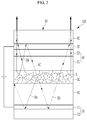
- FIG. 1 is a schematic cross-sectional view of an electronic device 100 according to an embodiment.
- An electronic device 100 includes a first electrode 10 and a second electrode 20 facing each other, an emission layer 30 including a plurality of quantum dots 3, wherein the emission layer is disposed between the first electrode 10 and the second electrode 20, a first charge auxiliary layer 40 disposed between the first electrode 10 and the emission layer 30, a second charge auxiliary layer 50 disposed between the emission layer 30 and the second electrode 20, and an optical functional layer 60 disposed on the second electrode 20 on a side opposite the emission layer 30. That is, the optical functional layer 60 and the emission layer 30 are on opposite sides of the second electrode 20.
- the electronic device 100 does not include the second charge auxiliary layer 50.
- the electronic device 100 may be an electro-luminescence device capable of generating light by flowing current to the emission layer 30 including the plurality of quantum dots 3 through the first electrode 10 and the second electrode 20.
- the electronic device 100 may generate light in a variety of wavelength regions depending upon the types of quantum dots in the plurality of quantum dots 3 included in the emission layer 30.
- the first electrode 10 includes a reflecting electrode
- the second electrode 20 includes a light-transmitting electrode.
- the light generated from the emission layer 30 may be emitted to the outside of the electronic device 100 through the upper side 62 of the optical functional layer 60 as shown in FIG. 1 .
- the first electrode 10 may be disposed directly on a suitable substrate.
- the first electrode 10 includes a material having a high reflectivity, it may reflect incident light that reaches to the first electrode 10.
- the first electrode 10 may act as a cathode.
- the first electrode 10 is paired with the second electrode 20 acting as an anode to flow a current through the emission layer 30.
- the first electrode 10 may include a first layer 11 having a work function of about 4.2 electron volts (eV) to about 4.7 eV, and an optically opaque second layer 12.
- the first layer 11 of the first electrode 10 has a work function of about 4.2 eV to about 4.6 eV, about 4.2 eV to about 4.5 eV, about 4.2 eV to about 4.4 eV, about 4.3 eV to about 4.7 eV, about 4.4 eV to about 4.7 eV, or about 4.5 eV to about 4.7 eV.
- the first layer 11 may be directly connected to a driving power source so may function to flow current to the emission layer 30.
- the first layer 11 may be formed on the second layer 12 with reference to FIG. 1 .
- the first layer 11 may be an optically transparent conductive material. Thereby, a portion of the light generated from the emission layer 30 may be passed through the first layer 11 and entered to the second layer 12.
- the first layer 11 may include an indium (In)-tin (Sn) oxide, an indium (In)-zinc (Zn) oxide, magnesium (Mg)-silver (Ag), aluminum (Al)-lithium (Li), magnesium (Mg)-indium (In), an indium (In) oxide, a tin (Sn) oxide, a gallium (Ga) oxide, a zinc (Zn) oxide, or a combination thereof
- the second layer 12 may include silver (Ag), aluminum (Al), zinc (Zn), gold (Au), iridium (Ir), copper (Cu), platinum (Pt), or a combination thereof.
- the second layer 12 may include a metal having a high reflectivity.
- the second layer 12 may include silver (Ag), aluminum (Al), zinc (Zn), gold (Au), iridium (Ir), copper (Cu), platinum (Pt), or a combination thereof.
- the light generated from the emission layer 30 is entered into the first layer 11 to an interface between the first layer 11 and the second layer 12, and reflected and returned to the emission layer 30.
- the second layer 12 may function as the reflecting electrode.
- the second electrode 20 may be an optically transparent material, so it may act as a light-transmitting electrode so that the light generated from the emission layer 30 may be transmitted through the second electrode 20.
- the second electrode 20 may include lithium, magnesium, aluminum, aluminum-lithium, calcium, magnesium-indium, magnesium-silver, or a combination thereof.
- the emission layer 30 may include a plurality of quantum dots 3.
- the emission layer 30 may be formed by coating a resin into which the plurality of quantum dots 3 is dispersed, and curing the same.
- the emission layer 30 is where the electrons and holes are delivered by the current supplied by the first electrode 10 and the second electrode 20.
- the electrons and holes recombine in the emission layer 30 to generate an exciton, and the generated exciton may emit light, at a wavelength corresponding to the size of the quantum dots in the plurality of quantum dots 3, while being transited from an excited state to a ground state.
- quantum dots 3 have a discontinuous energy bandgap by the quantum confinement effect, it may convert the incident light to light at a predetermined wavelength and emit the same. Thereby, the emission layer 30 including the plurality of quantum dots 3 may generate light having excellent color reproducibility and color purity. For example, the light emitted by the plurality of quantum dots 3 may have a narrow full width at half maximum (FWHM).
- FWHM narrow full width at half maximum
- the material of the plurality of quantum dots 3 is not particularly limited and includes any suitable quantum dot material, including those which are known in the art and/or commercially available.
- the quantum dots may include a Group II-VI compound, a Group III-V compound, a Group IV-VI compound, a Group IV compound, a Group II-III-VI compound, a Group I-II-IV-VI compound, or a combination thereof.
- the quantum dots may include a Group II-VI compound, a Group III-V compound, a Group IV-VI compound, a Group IV compound, or a combination thereof.
- the Group II-VI compound may be selected from a binary element compound selected from CdSe, CdTe, ZnS, ZnSe, ZnTe, ZnO, HgS, HgSe, HgTe, MgSe, MgS, and a combination thereof; a ternary element compound selected from CdSeS, CdSeTe, CdSTe, ZnSeS, ZnSeTe, ZnSTe, HgSeS, HgSeTe, HgSTe, CdZnS, CdZnSe, CdZnTe, CdHgS, CdHgSe, CdHgTe, HgZnS, HgZnSe, HgZnTe, MgZnSe, MgZnS, and a combination thereof; and a quaternary element compound selected from HgZnTeS, CdZnSeS, CdZnSeTe, Cd
- the Group III-V compound may be selected from a binary element compound selected from GaN, GaP, GaAs, GaSb, AIN, AlP, AlAs, AlSb, InN, InP, InAs, InSb, and a combination thereof; a ternary element compound selected from GaNP, GaNAs, GaNSb, GaPAs, GaPSb, AlNP, AlNAs, AlNSb, AlPAs, AlPSb, InNP, InNAs, InNSb, InPAs, InPSb, InZnP, and a combination thereof; and a quaternary element compound selected from GaAlNP, GaAlNAs, GaAlNSb, GaAlPAs, GaAlPSb, GalnNP, GalnNAs, GalnNSb, GalnPAs, GalnPSb, InAlNP, InAlNAs, InAlNSb, InAlPAs, InAlPSb, and a combination thereof.
- the Group IV-VI compound may be selected from a binary element compound selected from SnS, SnSe, SnTe, PbS, PbSe, PbTe, and a combination thereof; a ternary element compound selected from SnSeS, SnSeTe, SnSTe, PbSeS, PbSeTe, PbSTe, SnPbS, SnPbSe, SnPbTe, and a combination thereof; and a quaternary element compound selected from SnPbSSe, SnPbSeTe, SnPbSTe, and a combination thereof.
- the Group IV compound may include a single-element compound selected from Si, Ge, and a combination thereof; and a binary element compound selected from SiC, SiGe, and a combination thereof.
- the binary element compound, the ternary element compound or the quaternary element compound respectively exist in a uniform concentration in the quantum dot particle or in partially different concentrations in the same quantum dot particle.
- the quantum dots may have a core-shell structure wherein one quantum dot in the plurality of quantum dots 3 surrounds another quantum dot in the plurality of quantum dots 3.
- the core and shell may each have an interface, and an element of at least one of the core and the shell in the interface may have a concentration gradient wherein the concentration of the element(s) of the shell decreases toward the core.
- the plurality of quantum dots 3 may have one core of a quantum dot and multiple shells (i.e., multi-shell) surrounding the core.
- the multi-shell structure has at least two shells wherein each shell may be a single composition, an alloy, or a shell having a concentration gradient.
- the quantum dot materials of the shell may have a larger energy bandgap than the bandgap energy of the core, and thereby the quantum dot may exhibit a quantum confinement effect more effectively.
- the bandgap of the material of an outer shell may be of higher energy than the bandgap energy of the material of an inner shell that is closer to the core.
- the plurality of quantum dots 3 may emit light of a wavelength ranging from ultraviolet (UV) to infrared (IR) light.
- the plurality of quantum dots 3 may have quantum efficiency (QE) of greater than or equal to about 10 %, for example, greater than or equal to about 30 %, greater than or equal to about 50 %, greater than or equal to about 60 %, greater than or equal to about 70 %, or greater than or equal to about 90 %.
- QE quantum efficiency
- the quantum dots in the plurality of quantum dots 3 may be formed of the same materials or different materials.
- the quantum dots of the plurality of quantum dots 3 may have the same size or a different size from one another.
- the plurality of quantum dots 3 has characteristics such as emitting light in all directions. In the emission layer 30 including the plurality of quantum dots 3, it may be difficult to control the transport path of light in one predetermined direction.
- the electronic device 100 may include a transport path of light so that light is emitted (e.g., directed) to the outside of the electronic device 100 through the second electrode 20 which is a light-transmitting electrode, as the first electrode 10 includes the second layer 12 which is a reflecting electrode.
- the optical functional layer 60 may be formed on the second electrode 20 on a side opposite the emission layer 30.
- the optical functional layer 60 may include an optically transparent material, but may also function as a transflective layer which passes a portion of light that is at or near the wavelength corresponding to the predetermined resonance wavelength or wavelengths and reflects the remaining portions of light that are emitted from the emission layer.
- a microcavity structure may be formed in a region between the optical functional layer 60 and the first electrode 10 including the reflecting electrode.
- the microcavity structure means that the portion of light at a predetermined wavelength or wavelengths is amplified due to the constructive interference caused by repeatedly reflecting light between a reflecting layer and a transflective layer across an optical length.
- the first electrode 10 may function as a reflecting layer
- the optical functional layer 60 may function as a transflective layer.
- the portion of light near to the wavelength(s) corresponding to the resonance wavelength(s) of the microcavity is reinforced by the optical functional layer 60, and the other portion of light at other wavelengths are suppressed.
- the electronic device 100 in which the microcavity is formed by the optical functional layer 60 and the first electrode 10, for example, may amplify the portion of light corresponding to the objective wavelength range within the visible light wavelength range and emit the same to the outside.
- the wavelength range of light that is reinforced, for example amplified, by the microcavity may be determined by the physical properties of the materials in the electronic device 100, the optical properties of the transflective layer, an optical length between the transflective layer and the reflecting layer, and the like. More specifically, the properties of the microcavity of the electronic device 100 according to an embodiment may be preliminarily determined in part by a refractive index of the optical functional layer 60 which is a transflective layer.
- the optical functional layer 60 is not totally reflective at least at the interface with the second electrode 20, so the refractive index of the optical functional layer 60 may be the same as the refractive index of the second electrode 20, or the refractive index of the optical functional layer 60 may be greater than the refractive index of the second electrode 20.
- the optical functional layer 60 may have a refractive index of, for example, greater than or equal to about 1.2, for example, greater than or equal to about 1.5, for example, greater than or equal to about 1.7, for example, greater than or equal to about 2.2, and the refractive index may be, for example, less than or equal to about 2.8, for example, less than or equal to about 2.6, for example, less than or equal to about 2.5.
- the refractive index may be about 1.2 to about 2.8, about 1.5 to about 2.6, about 1.7 to about 2.5, about 2.2 to about 2.8, about 2.2 to about 2.6, or about 2.2 to about 2.5.
- the electronic device 100 may form a microcavity structure in the region between the optical functional layer 60 and the second layer 12 of the first electrode 10.
- the light wavelength range reinforced, for example amplified, by the microcavity may be also determined by the particular material(s) of the optical functional layer 60 and/or the thickness of the optical functional layer 60, in addition to the refractive index of the optical functional layer 60.
- the optical functional layer 60 may include an organic material including: a triarylamine-based compound including a triarylamine group in which the same or different aryl groups of the three aryl groups are substituted, a diarylamine-based compound including a diarylamine group in which same or different aryl groups of the two aryl groups are substituted, a carbazole-based compound in which the same or different aryl groups of the two aryl groups are substituted in the carbazole structure, or a combination thereof.
- a triarylamine-based compound including a triarylamine group in which the same or different aryl groups of the three aryl groups are substituted
- a diarylamine-based compound including a diarylamine group in which same or different aryl groups of the two aryl groups are substituted
- a carbazole-based compound in which the same or different aryl groups of the two aryl groups are substituted in the carbazole structure, or a combination thereof.
- the optical functional layer 60 may have a thickness t2 of, for example, greater than or equal to about 30 nanometers (nm), for example, greater than or equal to about 35 nm, for example, greater than or equal to about 40 nm, and for example, less than or equal to about 100 nm, for example, less than or equal to about 95 nm, for example, less than or equal to about 90 nm, for example, less than or equal to about 85 nm.
- the optical functional layer 60 may have a thickness t2 of about 30 nm to about 100 nm, about 35 nm to about 95 nm, or about 40 nm to about 85 nm.
- the optical functional layer 60 may function as a transflective layer for the predetermined wavelength region within a visible light wavelength region.
- the optical functional layer 60 may have a thickness of greater than or equal to about 30 nm, for example, greater than or equal to about 35 nm, for example, greater than or equal to about 40 nm, and for example, less than or equal to about 70 nm, for example, less than or equal to about 65 nm, for example, less than or equal to about 60 nm, for example, less than or equal to about 55 nm.
- the emission layer 30 emits a blue light and the optical functional layer 60 has a thickness of about 30 nm to about 70 nm, about 35 nm to about 65 nm, about 40 nm to about 60 nm, or about 40 nm to about 55 nm.
- the optical functional layer 60 may have a thickness of greater than or equal to about 65 nm, for example, greater than or equal to about 70 nm, for example, greater than or equal to about 75 nm, and for example, less than or equal to about 100 nm, for example, less than or equal to about 95 nm, for example, less than or equal to about 90 nm, for example, less than or equal to about 85 nm.
- the emission layer 30 emits a red light and the optical functional layer 60 has a thickness of about 65 nm to about 100 nm, about 70 nm to about 95 nm, about 75 nm to about 90 nm, or about 75 nm to about 85 nm.
- the wavelength range of light reinforced, for example amplified, by the microcavity may be determined by an optical length.
- the optical length corresponds to a distance between the first electrode 10 and the optical functional layer 60.
- a first charge auxiliary layer 40 and a second charge auxiliary layer 50 are auxiliary layers ( FIGS. 1 and 2 ) for improving the luminous efficiency of the emission layer 30, which function to control the charge carrier balance in the electronic device 100.
- the first charge auxiliary layer 40 and the second charge auxiliary layer 50 receive a current from the first electrode 10 and the second electrode 20, respectively, to generate holes or electrons, and function to transfer the holes and the electrons to the emission layer 30, respectively.
- the first charge auxiliary layer 40 may include an electron injecting and/or transporting layer
- the second charge auxiliary layer 50 may include a hole injecting and/or transporting layer.
- the first charge auxiliary layer 40 is an electron transport layer configured to transport electrons to the emission layer 30;
- the second charge auxiliary layer 50 may include a hole injection layer 52 configured to inject holes into the emission layer 30 and a hole transport layer 51 configured to transport holes to the emission layer 30.
- the hole transport layer 51 and the hole injection layer 52 may respectively include, for example, at least one selected from poly(3,4-ethylenedioxythiophene):poly(styrene sulfonate) (PEDOT:PSS), poly(9,9-dioctylfluorene-co-N-(4-butylphenyl)diphenylamine) (TFB), polyarylamine, poly(N-vinylcarbazole), polyaniline, polypyrrole, N,N,N',N'-tetrakis(4-methoxyphenyl)-benzidine (TPD), 4-bis[N-(1-naphthyl)-N-phenylamino]biphenyl ( ⁇ -NPD), 4,4',4"-tris[phenyl(m-tolyl)amino]triphenylamine (m-MTDATA), 4,4',4"-tris(N-carbazolyl)triphenylamine (TC
- the electronic device 100 is operated in an inverted method and may have a top emission structure emitting light through the optical functional layer 60, for example through the upper side 62 of the optical functional layer 60.
- the operating method and the emission structure of the electronic device 100 according to an embodiment are not necessarily limited thereto.
- an optical length which is one of the conditions for determining the properties of a microcavity.
- the optical length corresponds to a distance between the first electrode 10 and the optical functional layer 60, and is affected by the thickness of the emission layer 30, the thickness of the first charge auxiliary layer 40, and the thickness of the second charge auxiliary layer 50.
- the optical length of the microcavity may be determined by the thickness t1 of the first charge auxiliary layer 40, instead of the thickness of the emission layer 30 or the thickness of the second charge auxiliary layer 50.
- the electronic device 100 uses the emission layer 30 including the plurality of quantum dots 3 having isotropically luminous radiating characteristics.
- FIG. 2 is a cross-sectional view schematically showing the various exemplary light transporting paths in the electronic device 100 according to an embodiment.
- the plurality quantum dots 3 radiates light in all directions due to the isotropic light radiating characteristics.
- a part of the light is transported in a direction 5A to the second layer 12 of the first electrode 10, which is a reflecting electrode.
- a part of the generated light is transported in a direction 5B to the optical functional layer 60 and reflected in a direction 5C towards the second layer 12 of the first electrode 10, and then reflected in a direction 5D from the second layer 12 and transported to the optical functional layer 60.
- the light radiated by the plurality of quantum dots 3 is resonated by repeatedly reflecting between the second layer 12 and the optical functional layer 60 in the electronic device 100 and then amplified into light of a predetermined wavelength(s), and this light is ultimately emitted to the outside of the electronic device 100.
- the number of paths passing through the first charge auxiliary layer 40 is greater than the number of paths passing through each of the emission layer 30 and the second charge auxiliary layer 50 according to the repeating resonance pathways.
- the paths of passing light through the first charge auxiliary layer 40 may determine the optical length of microcavity. That is, according to an embodiment, the optical length of the microcavity is the distance between the optical functional layer 60 and the second layer 12 of the first electrode 10, and is measured along the light transporting paths 5C and 5D as shown in FIG. 2 .
- the first charge auxiliary layer 40 of the electronic device 100 is an electron transport layer, and the electron transport layer may include a zinc (Zn) oxide, a molybdenum (Mo) oxide, a tungsten (W) oxide, a nickel (Ni) oxide, a zirconium (Zr) oxide, a titanium (Ti) oxide, a nickel (Ni) oxide, a tin (Sn) oxide, or a combination thereof.
- the electron transport layer may have a thickness t1 of, for example, greater than or equal to about 20 nm, or for example, greater than or equal to about 25 nm, and for example, less than or equal to about 85 nm, for example, less than or equal to about 70 nm, for example, less than or equal to about 65 nm.
- the thickness t1 is about 20 nm to about 85 nm, about 25 nm to about 70 nm, or about 25 nm to about 65 nm.
- the first charge auxiliary layer 40 may have a thickness of, for example, greater than or equal to about 40 nm, for example, greater than or equal to about 45 nm, for example, greater than or equal to about 50 nm, and for example, less than or equal to about 70 nm, for example, less than or equal to about 65 nm.
- the emission layer 30 emits a red light and the thickness of the first charge auxiliary layer 40 is about 40 nm to about 70 nm, about 45 nm to about 65 nm, or about 50 nm to about 65 nm.
- the first charge auxiliary layer 40 may have a thickness of, for example, greater than or equal to about 20 nm, for example, greater than or equal to about 25 nm, and for example, less than or equal to about 50 nm, for example, less than or equal to about 45 nm, for example, less than or equal to about 40 nm.
- the emission layer 30 emits a blue light and the thickness of the first charge auxiliary layer 40 is about 20 nm to about 50 nm, about 25 nm to about 45 nm, or about 25 nm to about 40 nm.
- the electronic device 100 When the emission layer 30 including the plurality of quantum dots 3 is applied to an electro-luminescence structure, unlike the general organic light emitting diode, the electronic device 100 has a very low light extraction efficiency of about 25% due to the isotropically luminous radiating characteristics of the plurality of quantum dots 3.
- the organic light emitting diode may readily control the balance of the charge carrier by adjusting the inner elements of the device, it can provide a microcavity, but in a case of the quantum dot electro-luminescence device including the plurality of quantum dots 3, it is difficult to variously design the balance of the charge carrier by adjusting only the inner elements of the electronic device, so that the forming of a microcavity is more difficult.
- the electronic device 100 includes the optical functional layer 60, which is a transflective layer, disposed on the inside of the electronic device 100, so that a microcavity is formed in the quantum dot electro-luminescence device, and also the wavelength region of the microcavity may be further controlled by adjusting the thickness of the first charge auxiliary layer 40. Accordingly, the electronic device 100 according to an embodiment may have an excellent luminous efficiency since both the external quantum efficiency (EQE) and the light extraction efficiency are improved.
- EQE external quantum efficiency
- the electronic device may emit light having a narrower full width at half maximum (FWHM) and a less distortion of conduction band due to the defects, than the organic light emitting diode, so the emitted light may have a high color reproducibility and a high color purity.
- FWHM full width at half maximum
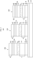
- a display device 1000 including an electronic device according to an embodiment is described with reference to FIG. 3 .
- FIG. 3 is a schematic cross-sectional view of a display device including an electronic device according to an embodiment.
- the display device 1000 includes a substrate 200, a driving circuit 300 formed on the substrate 200, and a first electronic device 100R, a second electronic device 100G, and a third electronic device 100B spaced apart from each other in a predetermined interval and disposed on the driving circuit 300.
- the first to third electronic devices 100R, 100G, and 100B have the same structure as in the electronic device 100, but the wavelengths of the lights emitted from each of the plurality of quantum dots 3R, 3G, and 3B are different from each other.
- the first electronic device 100R is a red device emitting a red light
- the second electronic device 100G is a green device emitting a green light
- the third electronic device 100B is a blue device emitting a blue light.
- the first to third electronic devices 100R, 100G, 100B may be pixels expressing red, green, and blue, respectively, in the display device 1000.
- the first to third electronic devices may respectively express magenta, yellow, cyan, or may express other colors.
- the substrate 200 which is a transparent insulation substrate, may be a soft material.
- the substrate 200 may include glass or a polymer material in a film having a glass transition temperature (Tg) of greater than about 150°C.
- Tg glass transition temperature
- it can include a COC (cycloolefin copolymer) or a COP (cycloolefin polymer) based material.
- the driving circuit 300 is disposed on the substrate 200 and independently connected with each of the first to third electronic devices 100R, 100G, and 100B.
- the driving circuit 300 may include at least one line including a scan line, a data line, a driving power source line, a common power source line, and the like, at least two of thin film transistors (TFT) connected to the wire and corresponding to one organic light emitting diode, and at least one capacitor, or the like.
- TFT thin film transistors
- the driving circuit 300 may have a variety of suitable structures, including the known structures in the art.
- each of the first to third electronic devices 100R, 100G, and 100B may each independently have a refractive index of, for example, greater than or equal to about 1.2, for example, greater than or equal to about 1.5, for example, greater than or equal to about 1.7, for example, greater than or equal to about 2.2, and the refractive index may be, for example, less than or equal to about 2.8, for example, less than or equal to about 2.6, for example, less than or equal to about 2.5.
- the first to third electronic devices 100R, 100G, and 100B may each independently have a refractive index of about 1.2 to about 2.8, about 1.5 to about 2.6, about 1.7 to about 2.5, or about 2.2 to about 2.5.
- the devices may form each microcavity through the optical functional layer 60R, 60G, and 60B and the second layers 12R, 12G, and 12B.
- the thickness of the optical functional layer 60R, 60G, and 60B and/or the thickness of the first charge transport layer 40R, 40G, and 40B may be different from each other.
- the thickness t11 of the first charge transport layer 40R of the first electronic device may be greater than, for example thicker than, the thicknesses t12 and t13 of the first charge transport layers 40G and 40B of other electronic devices.
- the thickness t13 of the first charge transport layer 40B of the third electronic device may be less than, for example thinner than, the thickness t12 of the charge transport layer 40G of the second electronic device.
- the thickness t11 of the charge transport layer 40R of the first electronic device may be, for example, greater than or equal to about 40 nm, for example, greater than or equal to about 45 nm, for example, greater than or equal to about 50 nm, and for example, less than or equal to about 70 nm, for example, less than or equal to about 65 nm.
- the thickness t11 can be about 40 nm to about 70 nm, about 45 nm to about 65 nm, or about 50 nm to about 65 nm.
- the thickness t13 of the charge transport layer 40B of the third electronic device may be for example, greater than or equal to about 20 nm, for example, greater than or equal to about 25 nm, and for example, less than or equal to about 50 nm, for example, less than or equal to about 45 nm, for example, less than or equal to about 40 nm.
- the thickness t13 can be about 20 nm to about 50 nm, about 25 nm to about 45 nm, or about 25 nm to about 40 nm.
- the thickness t21 of the optical functional layer 60R of the first electronic device may be greater than, for example thicker than, the thicknesses t22 and t23 of the optical functional layers 60G and 60B of other electronic devices.
- the thickness t23 of the optical functional layer 60B of the third electronic device may be less than, for example thinner than, the thickness t22 of the optical functional layer 60G of the second electronic device.
- the optical functional layer 60R of the first electronic device may have a thickness t21 of, for example, greater than or equal to about 65 nm, for example, greater than or equal to about 70 nm, for example, greater than or equal to about 75 nm, and for example, less than or equal to about 100 nm, for example, less than or equal to about 95 nm, for example, less than or equal to about 90 nm, for example, less than or equal to about 85 nm.
- the thickness t21 can be about 65 nm to about 100 nm, about 70 nm to about 95 nm, about 75 nm to about 90 nm, or about 75 nm to about 85 nm.
- the optical functional layer 60B of the third electronic device may have a thickness t23 of, for example, greater than or equal to about 30 nm, for example, greater than or equal to about 35 nm, for example, greater than or equal to about 40 nm, and for example, less than or equal to about 70 nm, for example, less than or equal to about 65 nm, for example, less than or equal to about 60 nm, for example, less than or equal to about 55 nm.
- the thickness t23 can be about 30 nm to about 70 nm, about 35 nm to about 65 nm, about 40 nm to about 60 nm, or about 40 nm to about 55 nm.
- the first to third electronic devices 100R, 100G, and 100B may have different heights from each other.
- an embodiment is not necessarily limited thereto, but the refractive indexes of the optical functional layers 60R, 60G, and 60B of devices are different from each other, or the first to third electronic devices 100R, 100G, and 100B may have the same height by adjusting the thicknesses of second charge transport layers 50R, 50G, and 50B, emission layers 30R, 30G, and 30B and the like.
- the display device 1000 may express images having excellent color purity and color reproducibility through the quantum dot electro-luminescence element.
- the display device 1000 may express images having a high luminescence in a low power.
- An ITO layer is deposited in a thickness of 10 nm on a silver (Ag) reflector having a thickness of 100 nm, and a ZnO layer is formed thereon in a thickness of 36 nm. Thereafter, blue quantum dots which are dispersed in an organic solvent are coated thereon in a thickness of 25 nm and then cured at 80°C for 30 minutes under the nitrogen atmosphere to provide a blue emission layer.
- a 4,4',4"-tris(N-carbazolyl)-triphenylamine (TCTA) layer is formed on the obtained blue emission layer in a thickness of 25 nm, and a MoO 3 layer having a thickness of 10 nm and a magnesium-silver layer having a thickness of 12 nm are formed thereon.
- an optical functional layer including at least one of a triarylamine-based compound, a diarylamine-based compound, and a carbazole-based compound is formed on a magnesium-silver layer in a thickness of 51 nm to provide a blue light emitting element according to Example 1.
- a red light emitting element according to Example 2 is obtained in accordance with the same procedure as in Example 1, except that the ZnO layer is formed in a thickness of 60 nm instead of 36 nm; red quantum dots are dispersed in an organic solvent and coated instead of the blue quantum dots to provide a red emission layer; a carbazole-based compound-including layer is formed in a thickness of 52 nm instead of the TCTA layer; and the optical functional layer is formed in a thickness of 95 nm instead of the thickness of 51 nm.
- a red light emitting element according to Example 3 is obtained in accordance with the same procedure as in Example 2, except that the ZnO layer is formed in a thickness of 50 nm.
- a red light emitting element according to Example 4 is obtained in accordance with the same procedure as in Example 2, except that the ZnO layer is formed in a thickness of 55 nm.
- ITO indium tin oxide
- Blue quantum dots dispersed in an organic solvent are coated thereon in a thickness of 25 nm and then cured at 80°C for 30 minutes under the nitrogen atmosphere to provide a blue emission layer.
- a ZnO layer having a thickness of 36 nm is formed thereon, and an Al layer is deposited in a thickness of 120 nm to provide a blue light emitting element.
- a red light emitting element according to Comparative Example 2 is prepared in accordance with the same procedure as in Comparative Example 1, except that the a carbazole-based compound-including layer is formed in a thickness of 50 nm instead of the TCTA layer as in Example 1; the red quantum dots are coated instead of the blue quantum dots to provide a red emission layer.
- a blue light emitting element according to Comparative Example 3 is prepared in accordance with the same procedure as in Example 1, except that CBP [4,4'-bis (9-carbazolyl)-1,1'-biphenyl] layer that Firpic[bis (4,6-difluorophenylpyridinato-N,C2')picolinate iridium(III)] is doped is formed in a thickness of 40 nm, instead of forming the blue emission layer including the blue quantum dots.
- a voltage of 4 V is applied between the silver reflector and the ITO layer according to Example 1 and Comparative Example 1 to operate a light emitting element, and the spectral radiance is measured depending upon a wavelength region of light emitted from each light emitting element, and the results are shown in FIG. 4 .
- FIG. 4 is a graph showing a spectral radiance according to a wavelength region of Example 1 and Comparative Example 1.
- Example 1 has a higher spectral radiance at a blue light wavelength region from about 420 nm to about 480 nm than Comparative Example 1, which is 3.9 times higher at a maximum wavelength ( ⁇ max ).
- Example 1 provides a microcavity using the silver (Ag) reflector and the optical functional layer, so as to improve the light extraction efficiency for the blue light wavelength region compared to Comparative Example 1 having no microcavity structure.
- a light emitting element is driven by applying voltage of 4V between the silver reflector and the ITO layer according to Example 2 and Comparative Example 2, and the spectral radiance of light emitted from each light emitting element is measured according to a wavelength region, and the results are shown in FIG. 5 .
- FIG. 5 is a graph showing a spectral radiance according to a wavelength region of Example 2 and Comparative Example 2.
- Example 2 has a higher spectral radiance within a red light wavelength region from about 560 nm to about 700 nm than Comparative Example 2, which is 1.8 times higher at a ⁇ max .
- Example 2 forms microcavity using the silver (Ag) reflector and the optical functional layer, as in Example 1, so the light extraction efficiency for the red light wavelength region may be improved, compared to Comparative Example 2 having no microcavity.
- the improving effects on the light extraction efficiency for the red light wavelength region is less significant than improving the effect on the light extraction efficiency for the blue light wavelength region. This is estimated because the light extraction of the blue wavelength is insignificantly increased compared to the red wavelength due to the structural characteristics of Example 2 and Comparative Example 2 having a bottom structure of element.
- the light emitting element is driven by applying voltage of 4V between the ITO layer and the reflector according to Example 1 and Comparative Example 3, and the spectral radiance of light emitted from each light emitting element is measured according to a wavelength region, and the results are shown in FIG. 6 .
- FIG. 6 is a graph showing a spectral radiance of Example 1 and Comparative Example 3 according to a wavelength region;
- FIG. 7 is a view showing a CIE xy chromaticity diagram for Example 1; and
- FIG. 8 is for Comparative Example 3.
- the quantum dot electro-luminescence device according to Example 1 shows a spectral radiance in about 12% higher than in Comparative Example 3 including the general organic light emitting diode, and it shows a full width at half maximum (FWHM) and a central wavelength lower than Comparative Example 3.
- the quantum dot electro-luminescence device according to Example 1 may emit clearer blue light than the general organic light emitting diode.
- the quantum dot electro-luminescence device of Example 1 may emit blue light having higher color reproducibility and color purity than Comparative Example 3.
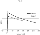
- the light emitting element is driven by applying voltage of 4 V to 6 V between the ITO layer of the silver reflector according to Example 3 and Example 4, and the spectral radiance according to wavelength region of light emitted from each light emitting element is measured, and the results are shown in FIG. 9 .
- the vertical axis in FIG. 9 indicates an external quantum efficiency, which is obtained by measuring a current density and a luminescence at the applied voltage and calculating based on the same.
- FIG. 9 is a graph showing external quantum efficiency (EQE) according to a luminescence in Example 3 and Example 4.
- Example 3 and Example 4 show quantum efficiency of greater than 3% at a luminescence of near to 0 cd/m 2 .
- the external quantum efficiency of the electronic device may be changed by only adjusting the thickness of ZnO layer without changing other conditions.
Landscapes
- Physics & Mathematics (AREA)
- Optics & Photonics (AREA)
- Chemical & Material Sciences (AREA)
- Engineering & Computer Science (AREA)
- Crystallography & Structural Chemistry (AREA)
- Inorganic Chemistry (AREA)
- Nanotechnology (AREA)
- Spectroscopy & Molecular Physics (AREA)
- Materials Engineering (AREA)
- Electroluminescent Light Sources (AREA)
- Led Devices (AREA)
Abstract
Description
- An electronic device and a display device including the same are disclosed.
- Quantum dots are a nanocrystal semiconductor material having a diameter of less than or equal to around 10 nm, and show quantum confinement effects. Quantum dots generate stronger intensity light in a narrower wavelength region than the commonly used phosphor. Quantum dots emit light while the excited electrons are transited from a conduction band to a valence band and emitted wavelengths vary based on a particle size of the quantum dots. Quantum dots can therefore be used obtain light in a desirable wavelength region by adjusting the size of the quantum dots.
- Advantages to electronic devices having an emission layer including quantum dots include reduced production costs compared to organic light emitting diode (OLED) devices using an emission layer including phosphorescence and/or phosphor material. Additionally, different colors may be emitted by changing the size of the quantum dots, whereas OLED devices require the use of different organic materials in the emission layer for each emitted color of light.
- The luminous efficiency of the emission layer including quantum dots is determined by an external quantum efficiency of quantum dots, a balance of charge carrier, and light extraction efficiency, and the like. There remains a need to improve the luminous efficiency of the quantum dot emission layer to provide more advanced electronic devices.
- An embodiment provides an electronic device having excellent luminous efficiency by improving light extraction efficiency, and a display device including the same.
- According to an embodiment, an electronic device includes a first electrode and a second electrode facing each other; an emission layer including a plurality of quantum dots, wherein the emission layer is disposed between the first electrode and the second electrode ; a first charge auxiliary layer disposed between the first electrode and the emission layer; and an optical functional layer disposed on the second electrode on a side opposite the emission layer, wherein the first electrode includes a reflecting electrode, wherein the second electrode is a light-transmitting electrode, wherein a region between the optical functional layer and the first electrode comprises a microcavity structure, and wherein a refractive index of the optical functional layer is greater than or equal to a refractive index of the second electrode.
- The refractive index of the optical functional layer may range from about 1.5 to about 2.5.
- The optical functional layer may include a triarylamine compound, a diarylamine compound, a carbazole compound, or a combination thereof.
- The emission layer may emit a blue light, and a thickness of the optical functional layer may range from about 40 nanometers to about 60 nanometers.
- The emission layer may emit a red light, and a thickness of the optical functional layer may range from about 70 nanometers to about 95 nanometers.
- The first charge auxiliary layer may include at least one electron transport layer.
- The at least one electron transport layer may include a zinc oxide, a molybdenum oxide, a tungsten oxide, a nickel oxide, or a combination thereof.
- The emission layer may emit a blue light, and a thickness of the at least one electron transport layer may range from about 25 nanometers to about 45 nanometers.
- The emission layer may emit a red light, and a thickness of the at least one electron transport layer may range from about 45 nanometers to about 80 nanometers.
- The first electrode may include a first layer having a work function of about 4.2 electron volts to about 4.7 electron volts, and an optically opaque second layer.
- The first layer may include an indium-tin oxide, an indium-zinc oxide, magnesium-silver, aluminum-lithium, magnesium-indium, an indium oxide, a tin oxide, a gallium oxide, a zinc oxide, or a combination thereof, and the second layer may include silver, aluminum, zinc, gold, iridium, copper, platinum, or a combination thereof.
- The second layer may include silver, aluminum, zinc, gold, iridium, copper, platinum, or a combination thereof.
- The quantum dots may include a Group II-VI compound, a Group III-V compound, a Group IV-VI compound, a Group IV compound, a Group II-III-VI compound, a Group I-II-IV-VI compound, or a combination thereof.
- According to another embodiment, a display device includes a first electronic device including a first quantum dot emitting light in a first wavelength region; a second electronic device including a second quantum dot emitting light in a shorter second wavelength region than the first wavelength region; and a third electronic device including a third quantum dot emitting light in a shorter third wavelength region than the second wavelength region, wherein each of the first electronic device, the second electronic device, and the third electronic device further includes a first electrode and a second electrode facing each other, an emission layer disposed between the first electrode and the second electrode, wherein the emission layer includes the first quantum dot, the second quantum dot, or the third quantum dot, a charge transport layer disposed between the emission layer and the first electrode, and an optical functional layer disposed on the second electrode on a side opposite the emission layer, wherein the first electrode includes a reflecting electrode, wherein the second electrode is a light-transmitting electrode, wherein a region between the optical functional layer and the first electrode comprises a microcavity structure, wherein a refractive index of the optical functional layer is greater than or equal to a refractive index of the second electrode, and wherein a thickness of the charge transport layer of the first electronic device, a thickness of the charge transport layer of the second electronic device, and a thickness of the charge transport layer of the third electronic device are different.
- The refractive index of the optical functional layer may range from about 1.5 to about 2.5.
- The thickness of the charge transport layer of the first electronic device may be greater than the thickness of the charge transport layer of the second electronic device and the thickness of the charge transport layer of the third electronic device.
- The thickness of the charge transport layer of the third electronic device may be less than the thickness of the charge transport layer of the second electronic device.
- The thickness of the charge transport layer of the first electronic device may range from about 45 nanometers to about 80 nanometers, and the thickness of the charge transport layer of the third electronic device may range from about 25 nanometers to about 45 nanometers.
- The thickness of the optical functional layer of the first electronic device, the thickness of the optical functional layer of the second electronic device, and the thickness of the optical functional layer of the third electronic device may be different.
- The thickness of the optical functional layer of the first electronic device may be greater than the thickness of the optical functional layer of the second electronic device and the thickness of the optical functional layer of the third electronic devices.
- The thickness of the optical functional layer of the third electronic device may be less than the thickness of the optical functional layer of the second electronic device.
- These and/or other aspects will become apparent and more readily appreciated from the following description of the embodiments, taken in conjunction with the accompanying drawings in which:
-
FIG. 1 is a schematic cross-sectional view of an electronic device according to an embodiment, -
FIG. 2 is a schematic cross-sectional view of a light transport path in an electronic device according to an embodiment, -
FIG. 3 is a schematic cross-sectional view of a display device including an electronic device according to an embodiment, -
FIG. 4 is a graph of spectral radiance (watt per steradian per square meter per nanometer, W sr-1 m-2 nm-1) versus wavelength (nanometer, nm) showing the spectral radiance according to a wavelength region in Example 1 and Comparative Example 1, -
FIG. 5 is a graph of spectral radiance (W sr-1 m-2 nm-1) versus wavelength (nm) showing the spectral radiance according to a wavelength region in Example 2 and Comparative Example 2, -
FIG. 6 is a graph of spectral radiance (W sr-1 m-2 nm-1) versus wavelength (nm) showing the spectral radiance according to a wavelength region in Example 1 and Comparative Example 3, -
FIGS. 7 and8 are graphs of CIE (y) versus CIE(x) showing CIE xy chromaticity coordinates for Example 1 and Comparative Example 3, respectively, and -
FIG. 9 is a graph of external quantum efficiency (EQE) (%) versus luminance (candela per square meter, cd/m2) showing the change in external quantum efficiency (EQE) according to luminance of Example 3 and Example 4. - Embodiments of the present disclosure will hereinafter be described in detail with reference to the accompanying drawings, in which various embodiments are shown. However, this disclosure may be embodied in many different forms, and is not to be construed as limited to the embodiments set forth herein.
- In the drawings, the thickness of layers, films, panels, regions, etc., are exaggerated for clarity. Like reference numerals designate like elements throughout the specification. It will be understood that when an element such as a layer, film, region, or substrate is referred to as being "on" another element, it can be directly on the other element or intervening elements may also be present. In contrast, when an element is referred to as being "directly on" another element, there are no intervening elements present.
- It will be understood that, although the terms "first," "second," "third" etc. may be used herein to describe various elements, components, regions, layers and/or sections, these elements, components, regions, layers and/or sections should not be limited by these terms. These terms are only used to distinguish one element, component, region, layer or section from another element, component, region, layer or section. Thus, "a first element," "component," "region," "layer" or "section" discussed below could be termed a second element, component, region, layer or section without departing from the teachings herein.
- The terminology used herein is for the purpose of describing particular embodiments only and is not intended to be limiting. As used herein, the singular forms "a," "an," and "the" are intended to include the plural forms, including "at least one," unless the content clearly indicates otherwise. "Or" means "and/or." As used herein, the term "and/or" includes any and all combinations of one or more of the associated listed items. It will be further understood that the terms "comprises" and/or "comprising," or "includes" and/or "including" when used in this specification, specify the presence of stated features, regions, integers, steps, operations, elements, and/or components, but do not preclude the presence or addition of one or more other features, regions, integers, steps, operations, elements, components, and/or groups thereof.
- Spatially relative terms, such as "beneath," "under," "below," "lower," "above," "upper" and the like, may be used herein for ease of description to describe one element or feature's relationship to another element(s) or feature(s) as illustrated in the figures. It will be understood that the spatially relative terms are intended to encompass different orientations of the device in use or operation in addition to the orientation depicted in the figures. For example, if the device in the figures is turned over, elements described as "below" or "beneath" other elements or features would then be oriented "above" the other elements or features. Thus, the exemplary term "below" can encompass both an orientation of above and below. The device may be otherwise oriented (rotated 90 degrees or at other orientations) and the spatially relative descriptors used herein interpreted accordingly.
- "About" or "approximately" as used herein is inclusive of the stated value and means within an acceptable range of deviation for the particular value as determined by one of ordinary skill in the art, considering the measurement in question and the error associated with measurement of the particular quantity (i.e., the limitations of the measurement system). For example, "about" can mean within one or more standard deviations, or within ± 30%, 20%, 10%, 5% of the stated value.
- Unless otherwise defined, all terms (including technical and scientific terms) used herein have the same meaning as commonly understood by one of ordinary skill in the art to which this disclosure belongs. It will be further understood that terms, such as those defined in commonly used dictionaries, should be interpreted as having a meaning that is consistent with their meaning in the context of the relevant art and the present disclosure, and will not be interpreted in an idealized or overly formal sense unless expressly so defined herein.
- Exemplary embodiments are described herein with reference to cross section illustrations that are schematic illustrations of idealized embodiments. As such, variations from the shapes of the illustrations as a result, for example, of manufacturing techniques and/or tolerances, are to be expected. Thus, embodiments described herein should not be construed as limited to the particular shapes of regions as illustrated herein but are to include deviations in shapes that result, for example, from manufacturing. For example, a region illustrated or described as flat may have rough and/or nonlinear features. Moreover, sharp angles that are illustrated may be rounded. Thus, the regions illustrated in the figures are schematic in nature and their shapes are not intended to illustrate the precise shape of a region and are not intended to limit the scope of the present claims.
-
FIG. 1 is a schematic cross-sectional view of anelectronic device 100 according to an embodiment. - An
electronic device 100 according to an embodiment includes afirst electrode 10 and asecond electrode 20 facing each other, anemission layer 30 including a plurality ofquantum dots 3, wherein the emission layer is disposed between thefirst electrode 10 and thesecond electrode 20, a first chargeauxiliary layer 40 disposed between thefirst electrode 10 and theemission layer 30, a second chargeauxiliary layer 50 disposed between theemission layer 30 and thesecond electrode 20, and an opticalfunctional layer 60 disposed on thesecond electrode 20 on a side opposite theemission layer 30. That is, the opticalfunctional layer 60 and theemission layer 30 are on opposite sides of thesecond electrode 20. In an embodiment, theelectronic device 100 does not include the second chargeauxiliary layer 50. - The
electronic device 100 may be an electro-luminescence device capable of generating light by flowing current to theemission layer 30 including the plurality ofquantum dots 3 through thefirst electrode 10 and thesecond electrode 20. Theelectronic device 100 may generate light in a variety of wavelength regions depending upon the types of quantum dots in the plurality ofquantum dots 3 included in theemission layer 30. - In an embodiment, as the
first electrode 10 includes a reflecting electrode, and thesecond electrode 20 includes a light-transmitting electrode. In theelectronic device 100, the light generated from theemission layer 30 may be emitted to the outside of theelectronic device 100 through theupper side 62 of the opticalfunctional layer 60 as shown inFIG. 1 . - Even though not shown in
FIG. 1 , thefirst electrode 10 may be disposed directly on a suitable substrate. As thefirst electrode 10 includes a material having a high reflectivity, it may reflect incident light that reaches to thefirst electrode 10. In an embodiment, thefirst electrode 10 may act as a cathode. Thefirst electrode 10 is paired with thesecond electrode 20 acting as an anode to flow a current through theemission layer 30. - In an embodiment, the
first electrode 10 may include afirst layer 11 having a work function of about 4.2 electron volts (eV) to about 4.7 eV, and an optically opaquesecond layer 12. In an embodiment, thefirst layer 11 of thefirst electrode 10 has a work function of about 4.2 eV to about 4.6 eV, about 4.2 eV to about 4.5 eV, about 4.2 eV to about 4.4 eV, about 4.3 eV to about 4.7 eV, about 4.4 eV to about 4.7 eV, or about 4.5 eV to about 4.7 eV. - The
first layer 11 may be directly connected to a driving power source so may function to flow current to theemission layer 30. Thefirst layer 11 may be formed on thesecond layer 12 with reference toFIG. 1 . Thefirst layer 11 may be an optically transparent conductive material. Thereby, a portion of the light generated from theemission layer 30 may be passed through thefirst layer 11 and entered to thesecond layer 12. In an embodiment, thefirst layer 11 may include an indium (In)-tin (Sn) oxide, an indium (In)-zinc (Zn) oxide, magnesium (Mg)-silver (Ag), aluminum (Al)-lithium (Li), magnesium (Mg)-indium (In), an indium (In) oxide, a tin (Sn) oxide, a gallium (Ga) oxide, a zinc (Zn) oxide, or a combination thereof, and thesecond layer 12 may include silver (Ag), aluminum (Al), zinc (Zn), gold (Au), iridium (Ir), copper (Cu), platinum (Pt), or a combination thereof. - The
second layer 12 may include a metal having a high reflectivity. In an embodiment, thesecond layer 12 may include silver (Ag), aluminum (Al), zinc (Zn), gold (Au), iridium (Ir), copper (Cu), platinum (Pt), or a combination thereof. Thereby, the light generated from theemission layer 30 is entered into thefirst layer 11 to an interface between thefirst layer 11 and thesecond layer 12, and reflected and returned to theemission layer 30. In other words, thesecond layer 12 may function as the reflecting electrode. - The
second electrode 20 may be an optically transparent material, so it may act as a light-transmitting electrode so that the light generated from theemission layer 30 may be transmitted through thesecond electrode 20. In an embodiment, thesecond electrode 20 may include lithium, magnesium, aluminum, aluminum-lithium, calcium, magnesium-indium, magnesium-silver, or a combination thereof. - The
emission layer 30 may include a plurality ofquantum dots 3. Theemission layer 30 may be formed by coating a resin into which the plurality ofquantum dots 3 is dispersed, and curing the same. - The
emission layer 30 is where the electrons and holes are delivered by the current supplied by thefirst electrode 10 and thesecond electrode 20. The electrons and holes recombine in theemission layer 30 to generate an exciton, and the generated exciton may emit light, at a wavelength corresponding to the size of the quantum dots in the plurality ofquantum dots 3, while being transited from an excited state to a ground state. - As
quantum dots 3 have a discontinuous energy bandgap by the quantum confinement effect, it may convert the incident light to light at a predetermined wavelength and emit the same. Thereby, theemission layer 30 including the plurality ofquantum dots 3 may generate light having excellent color reproducibility and color purity. For example, the light emitted by the plurality ofquantum dots 3 may have a narrow full width at half maximum (FWHM). - In an embodiment, the material of the plurality of
quantum dots 3 is not particularly limited and includes any suitable quantum dot material, including those which are known in the art and/or commercially available. For example, the quantum dots may include a Group II-VI compound, a Group III-V compound, a Group IV-VI compound, a Group IV compound, a Group II-III-VI compound, a Group I-II-IV-VI compound, or a combination thereof. - For example, the quantum dots may include a Group II-VI compound, a Group III-V compound, a Group IV-VI compound, a Group IV compound, or a combination thereof.
- The Group II-VI compound may be selected from a binary element compound selected from CdSe, CdTe, ZnS, ZnSe, ZnTe, ZnO, HgS, HgSe, HgTe, MgSe, MgS, and a combination thereof; a ternary element compound selected from CdSeS, CdSeTe, CdSTe, ZnSeS, ZnSeTe, ZnSTe, HgSeS, HgSeTe, HgSTe, CdZnS, CdZnSe, CdZnTe, CdHgS, CdHgSe, CdHgTe, HgZnS, HgZnSe, HgZnTe, MgZnSe, MgZnS, and a combination thereof; and a quaternary element compound selected from HgZnTeS, CdZnSeS, CdZnSeTe, CdZnSTe, CdHgSeS, CdHgSeTe, CdHgSTe, HgZnSeS, HgZnSeTe, HgZnSTe, and a combination thereof.
- The Group III-V compound may be selected from a binary element compound selected from GaN, GaP, GaAs, GaSb, AIN, AlP, AlAs, AlSb, InN, InP, InAs, InSb, and a combination thereof; a ternary element compound selected from GaNP, GaNAs, GaNSb, GaPAs, GaPSb, AlNP, AlNAs, AlNSb, AlPAs, AlPSb, InNP, InNAs, InNSb, InPAs, InPSb, InZnP, and a combination thereof; and a quaternary element compound selected from GaAlNP, GaAlNAs, GaAlNSb, GaAlPAs, GaAlPSb, GalnNP, GalnNAs, GalnNSb, GalnPAs, GalnPSb, InAlNP, InAlNAs, InAlNSb, InAlPAs, InAlPSb, and a combination thereof. The Group IV-VI compound may be selected from a binary element compound selected from SnS, SnSe, SnTe, PbS, PbSe, PbTe, and a combination thereof; a ternary element compound selected from SnSeS, SnSeTe, SnSTe, PbSeS, PbSeTe, PbSTe, SnPbS, SnPbSe, SnPbTe, and a combination thereof; and a quaternary element compound selected from SnPbSSe, SnPbSeTe, SnPbSTe, and a combination thereof.
- The Group IV compound may include a single-element compound selected from Si, Ge, and a combination thereof; and a binary element compound selected from SiC, SiGe, and a combination thereof.
- The binary element compound, the ternary element compound or the quaternary element compound respectively exist in a uniform concentration in the quantum dot particle or in partially different concentrations in the same quantum dot particle. The quantum dots may have a core-shell structure wherein one quantum dot in the plurality of
quantum dots 3 surrounds another quantum dot in the plurality ofquantum dots 3. The core and shell may each have an interface, and an element of at least one of the core and the shell in the interface may have a concentration gradient wherein the concentration of the element(s) of the shell decreases toward the core. In addition, the plurality ofquantum dots 3 may have one core of a quantum dot and multiple shells (i.e., multi-shell) surrounding the core. The multi-shell structure has at least two shells wherein each shell may be a single composition, an alloy, or a shell having a concentration gradient. - In the plurality of
quantum dots 3, the quantum dot materials of the shell may have a larger energy bandgap than the bandgap energy of the core, and thereby the quantum dot may exhibit a quantum confinement effect more effectively. In case of a multi-shell type structure, the bandgap of the material of an outer shell may be of higher energy than the bandgap energy of the material of an inner shell that is closer to the core. In this case, the plurality ofquantum dots 3 may emit light of a wavelength ranging from ultraviolet (UV) to infrared (IR) light. - The plurality of
quantum dots 3 may have quantum efficiency (QE) of greater than or equal to about 10 %, for example, greater than or equal to about 30 %, greater than or equal to about 50 %, greater than or equal to about 60 %, greater than or equal to about 70 %, or greater than or equal to about 90 %. - The quantum dots in the plurality of
quantum dots 3 may be formed of the same materials or different materials. In addition, the quantum dots of the plurality ofquantum dots 3 may have the same size or a different size from one another. - The plurality of
quantum dots 3 has characteristics such as emitting light in all directions. In theemission layer 30 including the plurality ofquantum dots 3, it may be difficult to control the transport path of light in one predetermined direction. However, theelectronic device 100 according to an embodiment may include a transport path of light so that light is emitted (e.g., directed) to the outside of theelectronic device 100 through thesecond electrode 20 which is a light-transmitting electrode, as thefirst electrode 10 includes thesecond layer 12 which is a reflecting electrode. - In an embodiment, the optical
functional layer 60 may be formed on thesecond electrode 20 on a side opposite theemission layer 30. The opticalfunctional layer 60 may include an optically transparent material, but may also function as a transflective layer which passes a portion of light that is at or near the wavelength corresponding to the predetermined resonance wavelength or wavelengths and reflects the remaining portions of light that are emitted from the emission layer. Thus, in an embodiment, a microcavity structure may be formed in a region between the opticalfunctional layer 60 and thefirst electrode 10 including the reflecting electrode. - The microcavity structure means that the portion of light at a predetermined wavelength or wavelengths is amplified due to the constructive interference caused by repeatedly reflecting light between a reflecting layer and a transflective layer across an optical length. In the
electronic device 100 according to an embodiment, thefirst electrode 10 may function as a reflecting layer, and the opticalfunctional layer 60 may function as a transflective layer. In other words, among the light generated from theemission layer 30, the portion of light near to the wavelength(s) corresponding to the resonance wavelength(s) of the microcavity is reinforced by the opticalfunctional layer 60, and the other portion of light at other wavelengths are suppressed. - Thus, the
electronic device 100 in which the microcavity is formed by the opticalfunctional layer 60 and thefirst electrode 10, for example, may amplify the portion of light corresponding to the objective wavelength range within the visible light wavelength range and emit the same to the outside. - The wavelength range of light that is reinforced, for example amplified, by the microcavity may be determined by the physical properties of the materials in the
electronic device 100, the optical properties of the transflective layer, an optical length between the transflective layer and the reflecting layer, and the like. More specifically, the properties of the microcavity of theelectronic device 100 according to an embodiment may be preliminarily determined in part by a refractive index of the opticalfunctional layer 60 which is a transflective layer. The opticalfunctional layer 60 is not totally reflective at least at the interface with thesecond electrode 20, so the refractive index of the opticalfunctional layer 60 may be the same as the refractive index of thesecond electrode 20, or the refractive index of the opticalfunctional layer 60 may be greater than the refractive index of thesecond electrode 20. - Meanwhile, the optical
functional layer 60 according to an embodiment may have a refractive index of, for example, greater than or equal to about 1.2, for example, greater than or equal to about 1.5, for example, greater than or equal to about 1.7, for example, greater than or equal to about 2.2, and the refractive index may be, for example, less than or equal to about 2.8, for example, less than or equal to about 2.6, for example, less than or equal to about 2.5. In an embodiment, the refractive index may be about 1.2 to about 2.8, about 1.5 to about 2.6, about 1.7 to about 2.5, about 2.2 to about 2.8, about 2.2 to about 2.6, or about 2.2 to about 2.5. As opticalfunctional layer 60 has this refractive index, theelectronic device 100 according to an embodiment may form a microcavity structure in the region between the opticalfunctional layer 60 and thesecond layer 12 of thefirst electrode 10. - In an embodiment, the light wavelength range reinforced, for example amplified, by the microcavity may be also determined by the particular material(s) of the optical
functional layer 60 and/or the thickness of the opticalfunctional layer 60, in addition to the refractive index of the opticalfunctional layer 60. - The optical
functional layer 60 according to an embodiment may include an organic material including: a triarylamine-based compound including a triarylamine group in which the same or different aryl groups of the three aryl groups are substituted, a diarylamine-based compound including a diarylamine group in which same or different aryl groups of the two aryl groups are substituted, a carbazole-based compound in which the same or different aryl groups of the two aryl groups are substituted in the carbazole structure, or a combination thereof. - In an embodiment, the optical
functional layer 60 may have a thickness t2 of, for example, greater than or equal to about 30 nanometers (nm), for example, greater than or equal to about 35 nm, for example, greater than or equal to about 40 nm, and for example, less than or equal to about 100 nm, for example, less than or equal to about 95 nm, for example, less than or equal to about 90 nm, for example, less than or equal to about 85 nm. In an embodiment, the opticalfunctional layer 60 may have a thickness t2 of about 30 nm to about 100 nm, about 35 nm to about 95 nm, or about 40 nm to about 85 nm. - If the optical
functional layer 60 satisfies at least one of the described conditions, it may function as a transflective layer for the predetermined wavelength region within a visible light wavelength region. - In an embodiment, when the
emission layer 30 of theelectronic device 100 emits a blue light, for example, the opticalfunctional layer 60 may have a thickness of greater than or equal to about 30 nm, for example, greater than or equal to about 35 nm, for example, greater than or equal to about 40 nm, and for example, less than or equal to about 70 nm, for example, less than or equal to about 65 nm, for example, less than or equal to about 60 nm, for example, less than or equal to about 55 nm. In an embodiment, theemission layer 30 emits a blue light and the opticalfunctional layer 60 has a thickness of about 30 nm to about 70 nm, about 35 nm to about 65 nm, about 40 nm to about 60 nm, or about 40 nm to about 55 nm. - In an embodiment, when the
emission layer 30 of theelectronic device 100 emits a red light, for example, the opticalfunctional layer 60 may have a thickness of greater than or equal to about 65 nm, for example, greater than or equal to about 70 nm, for example, greater than or equal to about 75 nm, and for example, less than or equal to about 100 nm, for example, less than or equal to about 95 nm, for example, less than or equal to about 90 nm, for example, less than or equal to about 85 nm. In an embodiment, theemission layer 30 emits a red light and the opticalfunctional layer 60 has a thickness of about 65 nm to about 100 nm, about 70 nm to about 95 nm, about 75 nm to about 90 nm, or about 75 nm to about 85 nm. - In an embodiment, the wavelength range of light reinforced, for example amplified, by the microcavity may be determined by an optical length. The optical length corresponds to a distance between the
first electrode 10 and the opticalfunctional layer 60. - A first charge
auxiliary layer 40 and a second chargeauxiliary layer 50 are auxiliary layers (FIGS. 1 and2 ) for improving the luminous efficiency of theemission layer 30, which function to control the charge carrier balance in theelectronic device 100. - In an embodiment, the first charge
auxiliary layer 40 and the second chargeauxiliary layer 50 receive a current from thefirst electrode 10 and thesecond electrode 20, respectively, to generate holes or electrons, and function to transfer the holes and the electrons to theemission layer 30, respectively. The first chargeauxiliary layer 40 may include an electron injecting and/or transporting layer, and the second chargeauxiliary layer 50 may include a hole injecting and/or transporting layer. - In an embodiment, the first charge
auxiliary layer 40 is an electron transport layer configured to transport electrons to theemission layer 30; the second chargeauxiliary layer 50 may include ahole injection layer 52 configured to inject holes into theemission layer 30 and ahole transport layer 51 configured to transport holes to theemission layer 30. - The
hole transport layer 51 and thehole injection layer 52 may respectively include, for example, at least one selected from poly(3,4-ethylenedioxythiophene):poly(styrene sulfonate) (PEDOT:PSS), poly(9,9-dioctylfluorene-co-N-(4-butylphenyl)diphenylamine) (TFB), polyarylamine, poly(N-vinylcarbazole), polyaniline, polypyrrole, N,N,N',N'-tetrakis(4-methoxyphenyl)-benzidine (TPD), 4-bis[N-(1-naphthyl)-N-phenylamino]biphenyl (α-NPD), 4,4',4"-tris[phenyl(m-tolyl)amino]triphenylamine (m-MTDATA), 4,4',4"-tris(N-carbazolyl)triphenylamine (TCTA), 1,1-bis[(di-4-tolyl amino)phenyl]cyclohexane (TAPC), and a combination thereof, but are not limited thereto, and may be selected according an energy level inside theelectronic device 100. - The
electronic device 100 according to an embodiment is operated in an inverted method and may have a top emission structure emitting light through the opticalfunctional layer 60, for example through theupper side 62 of the opticalfunctional layer 60. However, the operating method and the emission structure of theelectronic device 100 according to an embodiment are not necessarily limited thereto. - Meanwhile, as described above, an optical length which is one of the conditions for determining the properties of a microcavity. In an embodiment, the optical length corresponds to a distance between the
first electrode 10 and the opticalfunctional layer 60, and is affected by the thickness of theemission layer 30, the thickness of the first chargeauxiliary layer 40, and the thickness of the second chargeauxiliary layer 50. In an embodiment, in theelectronic device 100 the optical length of the microcavity may be determined by the thickness t1 of the first chargeauxiliary layer 40, instead of the thickness of theemission layer 30 or the thickness of the second chargeauxiliary layer 50. - This is because the
electronic device 100 according to an embodiment uses theemission layer 30 including the plurality ofquantum dots 3 having isotropically luminous radiating characteristics. -
FIG. 2 is a cross-sectional view schematically showing the various exemplary light transporting paths in theelectronic device 100 according to an embodiment. - Referring to
FIG. 2 , theplurality quantum dots 3 radiates light in all directions due to the isotropic light radiating characteristics. A part of the light is transported in adirection 5A to thesecond layer 12 of thefirst electrode 10, which is a reflecting electrode. In addition, a part of the generated light is transported in adirection 5B to the opticalfunctional layer 60 and reflected in adirection 5C towards thesecond layer 12 of thefirst electrode 10, and then reflected in adirection 5D from thesecond layer 12 and transported to the opticalfunctional layer 60. The light radiated by the plurality ofquantum dots 3 is resonated by repeatedly reflecting between thesecond layer 12 and the opticalfunctional layer 60 in theelectronic device 100 and then amplified into light of a predetermined wavelength(s), and this light is ultimately emitted to the outside of theelectronic device 100. - Looking to the light transporting paths in
FIG. 2 , the number of paths passing through the first chargeauxiliary layer 40 is greater than the number of paths passing through each of theemission layer 30 and the second chargeauxiliary layer 50 according to the repeating resonance pathways. Thereby, the paths of passing light through the first chargeauxiliary layer 40 may determine the optical length of microcavity. That is, according to an embodiment, the optical length of the microcavity is the distance between the opticalfunctional layer 60 and thesecond layer 12 of thefirst electrode 10, and is measured along thelight transporting paths FIG. 2 . - The first charge
auxiliary layer 40 of theelectronic device 100 according to an embodiment is an electron transport layer, and the electron transport layer may include a zinc (Zn) oxide, a molybdenum (Mo) oxide, a tungsten (W) oxide, a nickel (Ni) oxide, a zirconium (Zr) oxide, a titanium (Ti) oxide, a nickel (Ni) oxide, a tin (Sn) oxide, or a combination thereof. - In an embodiment, the electron transport layer may have a thickness t1 of, for example, greater than or equal to about 20 nm, or for example, greater than or equal to about 25 nm, and for example, less than or equal to about 85 nm, for example, less than or equal to about 70 nm, for example, less than or equal to about 65 nm. In an embodiment, the thickness t1 is about 20 nm to about 85 nm, about 25 nm to about 70 nm, or about 25 nm to about 65 nm. By adjusting the material and/or the thickness of the first charge
auxiliary layer 40 as describe above, theelectronic device 100 according to an embodiment may emit light reinforced by microcavity. - In an embodiment, when the
emission layer 30 of theelectronic device 100 emits a red light, the first chargeauxiliary layer 40 may have a thickness of, for example, greater than or equal to about 40 nm, for example, greater than or equal to about 45 nm, for example, greater than or equal to about 50 nm, and for example, less than or equal to about 70 nm, for example, less than or equal to about 65 nm. In an embodiment, theemission layer 30 emits a red light and the thickness of the first chargeauxiliary layer 40 is about 40 nm to about 70 nm, about 45 nm to about 65 nm, or about 50 nm to about 65 nm. - In an embodiment, when the
emission layer 30 of theelectronic device 100 emits a blue light, the first chargeauxiliary layer 40 may have a thickness of, for example, greater than or equal to about 20 nm, for example, greater than or equal to about 25 nm, and for example, less than or equal to about 50 nm, for example, less than or equal to about 45 nm, for example, less than or equal to about 40 nm. In an embodiment, theemission layer 30 emits a blue light and the thickness of the first chargeauxiliary layer 40 is about 20 nm to about 50 nm, about 25 nm to about 45 nm, or about 25 nm to about 40 nm. - When the
emission layer 30 including the plurality ofquantum dots 3 is applied to an electro-luminescence structure, unlike the general organic light emitting diode, theelectronic device 100 has a very low light extraction efficiency of about 25% due to the isotropically luminous radiating characteristics of the plurality ofquantum dots 3. In addition, as the organic light emitting diode may readily control the balance of the charge carrier by adjusting the inner elements of the device, it can provide a microcavity, but in a case of the quantum dot electro-luminescence device including the plurality ofquantum dots 3, it is difficult to variously design the balance of the charge carrier by adjusting only the inner elements of the electronic device, so that the forming of a microcavity is more difficult. - However, the
electronic device 100 according to an embodiment includes the opticalfunctional layer 60, which is a transflective layer, disposed on the inside of theelectronic device 100, so that a microcavity is formed in the quantum dot electro-luminescence device, and also the wavelength region of the microcavity may be further controlled by adjusting the thickness of the first chargeauxiliary layer 40. Accordingly, theelectronic device 100 according to an embodiment may have an excellent luminous efficiency since both the external quantum efficiency (EQE) and the light extraction efficiency are improved. - In addition, the electronic device according to an embodiment may emit light having a narrower full width at half maximum (FWHM) and a less distortion of conduction band due to the defects, than the organic light emitting diode, so the emitted light may have a high color reproducibility and a high color purity.
- Hereinafter, a
display device 1000 including an electronic device according to an embodiment is described with reference toFIG. 3 . -
FIG. 3 is a schematic cross-sectional view of a display device including an electronic device according to an embodiment. - The
display device 1000 according to an embodiment includes asubstrate 200, a drivingcircuit 300 formed on thesubstrate 200, and a firstelectronic device 100R, a secondelectronic device 100G, and a thirdelectronic device 100B spaced apart from each other in a predetermined interval and disposed on thedriving circuit 300. - The first to third
electronic devices electronic device 100, but the wavelengths of the lights emitted from each of the plurality ofquantum dots - In an embodiment, the first
electronic device 100R is a red device emitting a red light, the secondelectronic device 100G is a green device emitting a green light, and the thirdelectronic device 100B is a blue device emitting a blue light. In other words, the first to thirdelectronic devices display device 1000. - However, an embodiment is not necessarily limited thereto, but the first to third electronic devices may respectively express magenta, yellow, cyan, or may express other colors.
- The
substrate 200, which is a transparent insulation substrate, may be a soft material. Thesubstrate 200 may include glass or a polymer material in a film having a glass transition temperature (Tg) of greater than about 150°C. For example, it can include a COC (cycloolefin copolymer) or a COP (cycloolefin polymer) based material. - The driving
circuit 300 is disposed on thesubstrate 200 and independently connected with each of the first to thirdelectronic devices circuit 300 may include at least one line including a scan line, a data line, a driving power source line, a common power source line, and the like, at least two of thin film transistors (TFT) connected to the wire and corresponding to one organic light emitting diode, and at least one capacitor, or the like. The drivingcircuit 300 may have a variety of suitable structures, including the known structures in the art. - According to an embodiment, each of the first to third
electronic devices electronic devices functional layers functional layer second layers - In an embodiment, as lights emitted from each of the first to third
electronic devices functional layer charge transport layer - For example, the thickness t11 of the first
charge transport layer 40R of the first electronic device may be greater than, for example thicker than, the thicknesses t12 and t13 of the firstcharge transport layers charge transport layer 40B of the third electronic device may be less than, for example thinner than, the thickness t12 of thecharge transport layer 40G of the second electronic device. - For example, the thickness t11 of the
charge transport layer 40R of the first electronic device may be, for example, greater than or equal to about 40 nm, for example, greater than or equal to about 45 nm, for example, greater than or equal to about 50 nm, and for example, less than or equal to about 70 nm, for example, less than or equal to about 65 nm. In an embodiment, the thickness t11 can be about 40 nm to about 70 nm, about 45 nm to about 65 nm, or about 50 nm to about 65 nm. - In addition, for example, the thickness t13 of the
charge transport layer 40B of the third electronic device may be for example, greater than or equal to about 20 nm, for example, greater than or equal to about 25 nm, and for example, less than or equal to about 50 nm, for example, less than or equal to about 45 nm, for example, less than or equal to about 40 nm. In an embodiment, the thickness t13 can be about 20 nm to about 50 nm, about 25 nm to about 45 nm, or about 25 nm to about 40 nm. - In addition, for example, the thickness t21 of the optical
functional layer 60R of the first electronic device may be greater than, for example thicker than, the thicknesses t22 and t23 of the opticalfunctional layers functional layer 60B of the third electronic device may be less than, for example thinner than, the thickness t22 of the opticalfunctional layer 60G of the second electronic device. - The optical
functional layer 60R of the first electronic device may have a thickness t21 of, for example, greater than or equal to about 65 nm, for example, greater than or equal to about 70 nm, for example, greater than or equal to about 75 nm, and for example, less than or equal to about 100 nm, for example, less than or equal to about 95 nm, for example, less than or equal to about 90 nm, for example, less than or equal to about 85 nm. In an embodiment, the thickness t21 can be about 65 nm to about 100 nm, about 70 nm to about 95 nm, about 75 nm to about 90 nm, or about 75 nm to about 85 nm. - In an example, the optical
functional layer 60B of the third electronic device may have a thickness t23 of, for example, greater than or equal to about 30 nm, for example, greater than or equal to about 35 nm, for example, greater than or equal to about 40 nm, and for example, less than or equal to about 70 nm, for example, less than or equal to about 65 nm, for example, less than or equal to about 60 nm, for example, less than or equal to about 55 nm. In an embodiment, the thickness t23 can be about 30 nm to about 70 nm, about 35 nm to about 65 nm, about 40 nm to about 60 nm, or about 40 nm to about 55 nm. - By providing different thicknesses of optical
functional layers charge transport layers electronic devices electronic devices - However, an embodiment is not necessarily limited thereto, but the refractive indexes of the optical
functional layers electronic devices charge transport layers - As described herein, the
display device 1000 according to an embodiment may express images having excellent color purity and color reproducibility through the quantum dot electro-luminescence element. In addition, as each device has excellent luminous efficiency through microcavity, thedisplay device 1000 may express images having a high luminescence in a low power. - Hereinafter, the embodiments are illustrated in more detail with reference to examples. However, these examples are exemplary, and the present disclosure is not limited thereto.
- An ITO layer is deposited in a thickness of 10 nm on a silver (Ag) reflector having a thickness of 100 nm, and a ZnO layer is formed thereon in a thickness of 36 nm. Thereafter, blue quantum dots which are dispersed in an organic solvent are coated thereon in a thickness of 25 nm and then cured at 80°C for 30 minutes under the nitrogen atmosphere to provide a blue emission layer. A 4,4',4"-tris(N-carbazolyl)-triphenylamine (TCTA) layer is formed on the obtained blue emission layer in a thickness of 25 nm, and a MoO3 layer having a thickness of 10 nm and a magnesium-silver layer having a thickness of 12 nm are formed thereon. Then an optical functional layer including at least one of a triarylamine-based compound, a diarylamine-based compound, and a carbazole-based compound is formed on a magnesium-silver layer in a thickness of 51 nm to provide a blue light emitting element according to Example 1.
- A red light emitting element according to Example 2 is obtained in accordance with the same procedure as in Example 1, except that the ZnO layer is formed in a thickness of 60 nm instead of 36 nm; red quantum dots are dispersed in an organic solvent and coated instead of the blue quantum dots to provide a red emission layer; a carbazole-based compound-including layer is formed in a thickness of 52 nm instead of the TCTA layer; and the optical functional layer is formed in a thickness of 95 nm instead of the thickness of 51 nm.
- A red light emitting element according to Example 3 is obtained in accordance with the same procedure as in Example 2, except that the ZnO layer is formed in a thickness of 50 nm.
- A red light emitting element according to Example 4 is obtained in accordance with the same procedure as in Example 2, except that the ZnO layer is formed in a thickness of 55 nm.
- A poly(3,4-ethylenedioxythiophene):poly(styrene sulfonate) (PEDOT:PSS) layer having a thickness of 40 nm and a poly(9,9-dioctyl-fluorene-co-N-(4-butylphenyl)-diphenylamine) (TFB) layer having a thickness of 25 nm are formed on an indium tin oxide (ITO) electrode having a thickness of 150 nm. Blue quantum dots dispersed in an organic solvent are coated thereon in a thickness of 25 nm and then cured at 80°C for 30 minutes under the nitrogen atmosphere to provide a blue emission layer. A ZnO layer having a thickness of 36 nm is formed thereon, and an Al layer is deposited in a thickness of 120 nm to provide a blue light emitting element.
- A red light emitting element according to Comparative Example 2 is prepared in accordance with the same procedure as in Comparative Example 1, except that the a carbazole-based compound-including layer is formed in a thickness of 50 nm instead of the TCTA layer as in Example 1; the red quantum dots are coated instead of the blue quantum dots to provide a red emission layer.
- A blue light emitting element according to Comparative Example 3 is prepared in accordance with the same procedure as in Example 1, except that CBP [4,4'-bis (9-carbazolyl)-1,1'-biphenyl] layer that Firpic[bis (4,6-difluorophenylpyridinato-N,C2')picolinate iridium(III)] is doped is formed in a thickness of 40 nm, instead of forming the blue emission layer including the blue quantum dots.
- A voltage of 4 V is applied between the silver reflector and the ITO layer according to Example 1 and Comparative Example 1 to operate a light emitting element, and the spectral radiance is measured depending upon a wavelength region of light emitted from each light emitting element, and the results are shown in
FIG. 4 . -
FIG. 4 is a graph showing a spectral radiance according to a wavelength region of Example 1 and Comparative Example 1. - Referring to
FIG. 4 , it is confirmed that Example 1 has a higher spectral radiance at a blue light wavelength region from about 420 nm to about 480 nm than Comparative Example 1, which is 3.9 times higher at a maximum wavelength (λmax). In other words, it is confirmed that Example 1 provides a microcavity using the silver (Ag) reflector and the optical functional layer, so as to improve the light extraction efficiency for the blue light wavelength region compared to Comparative Example 1 having no microcavity structure. - A light emitting element is driven by applying voltage of 4V between the silver reflector and the ITO layer according to Example 2 and Comparative Example 2, and the spectral radiance of light emitted from each light emitting element is measured according to a wavelength region, and the results are shown in
FIG. 5 . -
FIG. 5 is a graph showing a spectral radiance according to a wavelength region of Example 2 and Comparative Example 2. - Referring to
FIG. 5 , it is confirmed that Example 2 has a higher spectral radiance within a red light wavelength region from about 560 nm to about 700 nm than Comparative Example 2, which is 1.8 times higher at a λmax. In other words, it is confirmed that Example 2 forms microcavity using the silver (Ag) reflector and the optical functional layer, as in Example 1, so the light extraction efficiency for the red light wavelength region may be improved, compared to Comparative Example 2 having no microcavity. - However, it is understood that the improving effects on the light extraction efficiency for the red light wavelength region is less significant than improving the effect on the light extraction efficiency for the blue light wavelength region. This is estimated because the light extraction of the blue wavelength is insignificantly increased compared to the red wavelength due to the structural characteristics of Example 2 and Comparative Example 2 having a bottom structure of element.
- The light emitting element is driven by applying voltage of 4V between the ITO layer and the reflector according to Example 1 and Comparative Example 3, and the spectral radiance of light emitted from each light emitting element is measured according to a wavelength region, and the results are shown in
FIG. 6 . -
FIG. 6 is a graph showing a spectral radiance of Example 1 and Comparative Example 3 according to a wavelength region;FIG. 7 is a view showing a CIE xy chromaticity diagram for Example 1; andFIG. 8 is for Comparative Example 3. - Referring to
FIG. 6 , the quantum dot electro-luminescence device according to Example 1 shows a spectral radiance in about 12% higher than in Comparative Example 3 including the general organic light emitting diode, and it shows a full width at half maximum (FWHM) and a central wavelength lower than Comparative Example 3. Particularly, looking at and comparingFIGS. 7 and8 , the quantum dot electro-luminescence device according to Example 1 may emit clearer blue light than the general organic light emitting diode. In other words, the quantum dot electro-luminescence device of Example 1 may emit blue light having higher color reproducibility and color purity than Comparative Example 3. - The light emitting element is driven by applying voltage of 4 V to 6 V between the ITO layer of the silver reflector according to Example 3 and Example 4, and the spectral radiance according to wavelength region of light emitted from each light emitting element is measured, and the results are shown in
FIG. 9 . - The vertical axis in
FIG. 9 indicates an external quantum efficiency, which is obtained by measuring a current density and a luminescence at the applied voltage and calculating based on the same. -
FIG. 9 is a graph showing external quantum efficiency (EQE) according to a luminescence in Example 3 and Example 4. - Referring to
FIG. 9 , it is confirmed that both Example 3 and Example 4 show quantum efficiency of greater than 3% at a luminescence of near to 0 cd/m2. Thereby, in the case of the electronic device formed with microcavity according to an embodiment, it is confirmed that the external quantum efficiency of the electronic device may be changed by only adjusting the thickness of ZnO layer without changing other conditions. - While this disclosure has been described in connection with what is presently considered to be practical example embodiments, it is to be understood that the invention is not limited to the disclosed embodiments, but, on the contrary, is intended to cover various modifications and equivalent arrangements included within the scope of the appended claims.
Claims (15)
- An electronic device comprising
a first electrode and a second electrode facing each other;
an emission layer comprising a plurality of quantum dots, wherein the emission layer is disposed between the first electrode and the second electrode;
a first charge auxiliary layer disposed between the first electrode and the emission layer; and
an optical functional layer disposed on the second electrode on a side opposite the emission layer,
wherein the first electrode comprises a reflecting electrode,
wherein the second electrode is a light-transmitting electrode,
wherein a region between the optical functional layer and the first electrode comprises a microcavity structure, and
wherein a refractive index of the optical functional layer is greater than or equal to a refractive index of the second electrode. - The electronic device of claim 1, wherein the refractive index of the optical functional layer ranges from 1.5 to 2.5.
- The electronic device of claim 1, wherein the optical functional layer comprises a triarylamine compound, a diarylamine compound, a carbazole compound, or a combination thereof.
- The electronic device of claim 1, wherein emission layer emits a blue light, and
a thickness of the optical functional layer ranges from 40 nanometers to 60 nanometers. - The electronic device of claim 1, wherein the emission layer emits a red light, and
a thickness of the optical functional layer ranges from 70 nanometers to 95 nanometers. - The electronic device of claim 1, wherein the first charge auxiliary layer comprises at least one electron transport layer, and preferably wherein the at least one electron transport layer comprises a zinc oxide, a molybdenum oxide, a tungsten oxide, a nickel oxide, or a combination thereof.
- The electronic device of claim 6, wherein the emission layer emits a blue light, and
a thickness of the at least one electron transport layer ranges from 25 nanometers to 45 nanometers. - The electronic device of claim 6, wherein the emission layer emits a red light, and
a thickness of the at least one electron transport layer ranges from 45 nanometers to 80 nanometers. - The electronic device of any preceding claim, wherein the first electrode comprises a first layer having a work function of 4.2 electron volts to 4.7 electron volts, and an optically opaque second layer, and preferably wherein the first layer comprises an indium-tin oxide, an indium-zinc oxide, magnesium-silver, aluminum-lithium, magnesium-indium, an indium oxide, a tin oxide, a gallium oxide, a zinc oxide, or a combination thereof, and the second layer comprises silver, aluminum, zinc, gold, iridium, copper, platinum, or a combination thereof.
- The electronic device of claim 9, wherein the second layer comprises silver, aluminum, zinc, gold, iridium, copper, platinum, or a combination thereof.
- The electronic device of any preceding claim, wherein the quantum dots comprise a Group II-VI compound, a Group III-V compound, a Group IV-VI compound, a Group IV compound, a Group II-III-VI compound, a Group I-II-IV-VI compound, or a combination thereof.
- A display device comprising
a first electronic device according to any preceding claim adapted to emit light in a first wavelength region;
a second electronic device according to any preceding claim adapted to emit light in a shorter second wavelength region than the first wavelength region; and
and a third electronic device according to any preceding claim adapted to emit light in a shorter third wavelength region than the second wavelength region,
and
wherein a thickness of the charge transport layer of the first electronic device, a thickness of the charge transport layer of the second electronic device, and a thickness of the charge transport layer of the third electronic device are different. - The display device of claim 12, wherein the thickness of the charge transport layer of the first electronic device is greater than the thickness of the charge transport layer of the second electronic device and the thickness of the charge transport layer of the third electronic device, and preferably wherein the thickness of the charge transport layer of the third electronic device is less than the thickness of the charge transport layer of the second electronic device.
- The display device of claim 13, wherein the thickness of the optical functional layer of the first electronic device, the thickness of the optical functional layer of the second electronic device, and the thickness of the optical functional layer of the third electronic device are different, and preferably wherein the thickness of the optical functional layer of the first electronic device is greater than the thickness of the optical functional layer of the second electronic device and the thickness of the optical functional layer of the third electronic device.
- The display device of claim 14, wherein the thickness of the optical functional layer of the third electronic device is less than the thickness of the optical functional layer of the second electronic device.
Applications Claiming Priority (1)
| Application Number | Priority Date | Filing Date | Title |
|---|---|---|---|
| KR1020160107064A KR102649300B1 (en) | 2016-08-23 | 2016-08-23 | Electric device, and display device comprising the same |
Publications (3)
| Publication Number | Publication Date |
|---|---|
| EP3288095A2 true EP3288095A2 (en) | 2018-02-28 |
| EP3288095A3 EP3288095A3 (en) | 2018-03-07 |
| EP3288095B1 EP3288095B1 (en) | 2024-03-27 |
Family
ID=59738143
Family Applications (1)
| Application Number | Title | Priority Date | Filing Date |
|---|---|---|---|
| EP17186686.6A Active EP3288095B1 (en) | 2016-08-23 | 2017-08-17 | Electric device, and display device comprising the same |
Country Status (4)
| Country | Link |
|---|---|
| US (2) | US10615356B2 (en) |
| EP (1) | EP3288095B1 (en) |
| KR (1) | KR102649300B1 (en) |
| CN (1) | CN107768541B (en) |
Families Citing this family (14)
| Publication number | Priority date | Publication date | Assignee | Title |
|---|---|---|---|---|
| KR20190119433A (en) * | 2018-04-12 | 2019-10-22 | 삼성전자주식회사 | Quantum dot device and electronic device |
| CN108649131B (en) * | 2018-05-11 | 2020-11-27 | 京东方科技集团股份有限公司 | Electroluminescent device and preparation method thereof, display panel and display device |
| KR102572134B1 (en) * | 2018-07-24 | 2023-08-28 | 삼성전자주식회사 | Quantum dot device and display device |
| JP2020173937A (en) * | 2019-04-09 | 2020-10-22 | 日本放送協会 | Quantum dot light emitting element and display device |
| WO2020227518A1 (en) * | 2019-05-08 | 2020-11-12 | Nanosys, Inc. | Nanostructure based display devices with improved light extraction efficiency |
| KR102718279B1 (en) * | 2019-09-23 | 2024-10-15 | 삼성전자주식회사 | Light emitting device and method of manufacturing the same and display device |
| US11133438B2 (en) * | 2019-11-20 | 2021-09-28 | Sharp Kabushiki Kaisha | Light-emitting device with transparent nanoparticle electrode |
| WO2021192157A1 (en) * | 2020-03-26 | 2021-09-30 | シャープ株式会社 | Light-emitting element, and display device |
| CN113206126B (en) * | 2020-06-02 | 2022-12-06 | 广东聚华印刷显示技术有限公司 | Display panel, preparation method thereof and display device |
| KR102820734B1 (en) * | 2020-07-17 | 2025-06-16 | 삼성디스플레이 주식회사 | Light emitting device and electronic apparatus comprising the same |
| US12464888B2 (en) * | 2020-09-23 | 2025-11-04 | Beijing Boe Technology Development Co., Ltd. | Quantum dot light emitting diode, manufacturing method thereof and display apparatus |
| KR102914549B1 (en) * | 2020-10-15 | 2026-01-20 | 삼성디스플레이 주식회사 | Display device and manufacturing method thereof |
| KR102926961B1 (en) * | 2021-06-28 | 2026-02-11 | 삼성전자주식회사 | Infrared photodiode and sensor and electronic device |
| WO2023205922A1 (en) * | 2022-04-24 | 2023-11-02 | 京东方科技集团股份有限公司 | Quantum dot light-emitting diode and preparation method therefor, and display panel |
Family Cites Families (33)
| Publication number | Priority date | Publication date | Assignee | Title |
|---|---|---|---|---|
| GB8703617D0 (en) * | 1986-02-20 | 1987-03-25 | Canon Kk | Electrophotographic photosensitive member |
| US6483236B1 (en) * | 2000-05-24 | 2002-11-19 | Eastman Kodak Company | Low-voltage organic light-emitting device |
| JP2002202737A (en) * | 2000-12-28 | 2002-07-19 | Nec Corp | Manufacturing method of light emitting element, light emitting element |
| KR100659530B1 (en) * | 2003-11-26 | 2006-12-19 | 삼성에스디아이 주식회사 | Full Color Organic Light Emitting Diode |
| US7309956B2 (en) | 2005-01-14 | 2007-12-18 | Eastman Kodak Company | Top-emitting OLED device with improved-off axis viewing performance |
| KR100883306B1 (en) * | 2005-03-24 | 2009-02-11 | 쿄세라 코포레이션 | Light emitting element, light emitting device having the light emitting element and manufacturing method thereof |
| US20070001581A1 (en) * | 2005-06-29 | 2007-01-04 | Stasiak James W | Nanostructure based light emitting devices and associated methods |
| US7404468B2 (en) | 2006-07-27 | 2008-07-29 | Hiwin Technologies Corp. | Elevator having second driving device |
| TWI338533B (en) * | 2006-09-18 | 2011-03-01 | Au Optronics Corp | White organic electroluminescent elements and display using the same |
| KR100835059B1 (en) | 2007-07-06 | 2008-06-03 | 삼성전자주식회사 | Quantum dot optical device |
| WO2009014707A2 (en) | 2007-07-23 | 2009-01-29 | Qd Vision, Inc. | Quantum dot light enhancement substrate and lighting device including same |
| JP2009087782A (en) * | 2007-09-28 | 2009-04-23 | Dainippon Printing Co Ltd | Method for manufacturing electroluminescence element |
| JP5176459B2 (en) | 2007-09-28 | 2013-04-03 | 大日本印刷株式会社 | White light emitting device |
| KR101458906B1 (en) | 2008-02-12 | 2014-11-13 | 삼성디스플레이 주식회사 | Organic light emitting diode display and method for manufacturing the same |
| US7816677B2 (en) | 2008-02-12 | 2010-10-19 | Samsung Electronics Co., Ltd. | Organic light emitting device |
| KR100922759B1 (en) * | 2008-02-26 | 2009-10-21 | 삼성모바일디스플레이주식회사 | Organic light emitting device |
| KR100953658B1 (en) * | 2008-06-05 | 2010-04-20 | 삼성모바일디스플레이주식회사 | Organic light emitting display |
| JP6000703B2 (en) * | 2011-08-12 | 2016-10-05 | キヤノン株式会社 | ORGANIC EL ELEMENT, AND LIGHT EMITTING DEVICE, IMAGE FORMING DEVICE, LIGHT EMITTING ELEMENT ARRAY, IMAGING DEVICE, DISPLAY DEVICE USING THE SAME |
| KR101339440B1 (en) * | 2012-01-26 | 2013-12-10 | 한국전자통신연구원 | Organic electroluminescent device and method for menufacturing thereof |
| KR20140010719A (en) | 2012-07-16 | 2014-01-27 | 삼성전자주식회사 | Light emitting diode device using charge accumulation and method of manufacturing the same |
| KR101954973B1 (en) * | 2012-09-19 | 2019-03-08 | 삼성디스플레이 주식회사 | Organic light emitting display |
| US9419174B2 (en) | 2012-09-26 | 2016-08-16 | University Of Florida Research Foundation, Inc. | Transparent quantum dot light-emitting diodes with dielectric/metal/dielectric electrode |
| CN103000813B (en) * | 2012-10-23 | 2015-09-09 | 京东方科技集团股份有限公司 | Light-emitting diode and preparation method thereof |
| CN108611591B (en) * | 2012-11-06 | 2021-05-04 | Oti领英有限公司 | Method for depositing a conductive coating on a surface |
| KR20140097775A (en) | 2013-01-30 | 2014-08-07 | 엘지디스플레이 주식회사 | Light emitting device |
| US9331298B2 (en) * | 2013-09-12 | 2016-05-03 | Board Of Trustees Of Michigan State University | Nanocluster based light emitting device |
| CN103500803B (en) * | 2013-10-21 | 2016-06-08 | 京东方科技集团股份有限公司 | A kind of recombination luminescence layer and making method, white light organic electroluminescent device |
| DE102014100405B4 (en) * | 2014-01-15 | 2025-10-02 | Pictiva Displays International Limited | Organic light-emitting device and method for producing an organic light-emitting device |
| KR102169016B1 (en) * | 2014-02-13 | 2020-10-23 | 삼성디스플레이 주식회사 | Organic light emitting display apparatus |
| KR102142620B1 (en) * | 2014-02-19 | 2020-08-10 | 삼성디스플레이 주식회사 | Organic light emitting display device |
| KR101614599B1 (en) * | 2014-04-09 | 2016-04-21 | 주식회사 두산 | Organic compound and organic electroluminescent device comprising the same |
| KR20160069555A (en) | 2014-12-08 | 2016-06-17 | 삼성디스플레이 주식회사 | Organic light emitting device and display device having the same |
| US10522787B1 (en) | 2018-11-27 | 2019-12-31 | Sharp Kabushiki Kaisha | High efficiency quantum dot LED structure |
-
2016
- 2016-08-23 KR KR1020160107064A patent/KR102649300B1/en active Active
-
2017
- 2017-04-10 US US15/483,651 patent/US10615356B2/en active Active
- 2017-08-17 EP EP17186686.6A patent/EP3288095B1/en active Active
- 2017-08-18 CN CN201710710708.XA patent/CN107768541B/en active Active
-
2020
- 2020-02-21 US US16/797,380 patent/US11018311B2/en active Active
Non-Patent Citations (1)
| Title |
|---|
| None |
Also Published As
| Publication number | Publication date |
|---|---|
| EP3288095B1 (en) | 2024-03-27 |
| EP3288095A3 (en) | 2018-03-07 |
| KR102649300B1 (en) | 2024-03-18 |
| CN107768541B (en) | 2022-03-18 |
| US20200194703A1 (en) | 2020-06-18 |
| US10615356B2 (en) | 2020-04-07 |
| US20180062030A1 (en) | 2018-03-01 |
| KR20180022134A (en) | 2018-03-06 |
| US11018311B2 (en) | 2021-05-25 |
| CN107768541A (en) | 2018-03-06 |
Similar Documents
| Publication | Publication Date | Title |
|---|---|---|
| US11018311B2 (en) | Device with quantum dot emissive layer and display device comprising the same | |
| US11581504B2 (en) | Electroluminescent device, and display device comprising the same | |
| US11818907B2 (en) | Quantum-dot light emitting device comprising solution processed charge generation junction and manufacturing method thereof | |
| US11594698B2 (en) | Electric device and display device comprising quantum dots with improved luminous efficiency | |
| US11011673B2 (en) | Quantum dot device and display device | |
| US11812627B2 (en) | Quantum dot device and electronic device | |
| US11139441B2 (en) | Quantum dot device and electronic device comprising an emissive quantum dot and a non-emissive quantum dot | |
| US20190157596A1 (en) | Quantum dot device and display device | |
| KR102618343B1 (en) | Quantum dot light emitting diode device | |
| US20170117496A1 (en) | Optoelectronic device including quantum dot | |
| US9761822B2 (en) | Light emitting diode and display device including the same | |
| KR102110780B1 (en) | Quantum dot light emitting device and the method for manufacturing thereof | |
| KR102001734B1 (en) | Quantum dot lightemitting device and manufacturing method therefor | |
| US20180175132A1 (en) | Organic light emitting diode and organic light emitting display device including the same | |
| US11784282B2 (en) | Quantum dot display device | |
| US20230403874A1 (en) | Light-emitting element, display device and light-emitting element manufacturing method | |
| KR101328477B1 (en) | Manufacturing method of organic light emitting diode | |
| CN114316942B (en) | Composite material, preparation method thereof and light-emitting diode | |
| CN118234278A (en) | Light emitting device and display device | |
| US20250107314A1 (en) | Display device and method for manufacturing the same | |
| KR102876709B1 (en) | Light emitting device using dual strcutre of self-emmissive quantum dot, method for manufacturing the same and method for generating light using the same | |
| KR102799396B1 (en) | Light emitting device based on quantum dots using zinc oxide to reduce quenching of photoluminescence and method for manufacturing the same | |
| KR20250152991A (en) | Light emitting device and method for generating light using self-emissive quantum dot | |
| KR20170091818A (en) | Light emitting diode |
Legal Events
| Date | Code | Title | Description |
|---|---|---|---|
| PUAI | Public reference made under article 153(3) epc to a published international application that has entered the european phase |
Free format text: ORIGINAL CODE: 0009012 |
|
| STAA | Information on the status of an ep patent application or granted ep patent |
Free format text: STATUS: THE APPLICATION HAS BEEN PUBLISHED |
|
| PUAL | Search report despatched |
Free format text: ORIGINAL CODE: 0009013 |
|
| AK | Designated contracting states |
Kind code of ref document: A2 Designated state(s): AL AT BE BG CH CY CZ DE DK EE ES FI FR GB GR HR HU IE IS IT LI LT LU LV MC MK MT NL NO PL PT RO RS SE SI SK SM TR |
|
| AX | Request for extension of the european patent |
Extension state: BA ME |
|
| AK | Designated contracting states |
Kind code of ref document: A3 Designated state(s): AL AT BE BG CH CY CZ DE DK EE ES FI FR GB GR HR HU IE IS IT LI LT LU LV MC MK MT NL NO PL PT RO RS SE SI SK SM TR |
|
| AX | Request for extension of the european patent |
Extension state: BA ME |
|
| RIC1 | Information provided on ipc code assigned before grant |
Ipc: H01L 51/50 20060101AFI20180126BHEP Ipc: H01L 51/52 20060101ALI20180126BHEP |
|
| STAA | Information on the status of an ep patent application or granted ep patent |
Free format text: STATUS: REQUEST FOR EXAMINATION WAS MADE |
|
| 17P | Request for examination filed |
Effective date: 20180726 |
|
| RBV | Designated contracting states (corrected) |
Designated state(s): AL AT BE BG CH CY CZ DE DK EE ES FI FR GB GR HR HU IE IS IT LI LT LU LV MC MK MT NL NO PL PT RO RS SE SI SK SM TR |
|
| STAA | Information on the status of an ep patent application or granted ep patent |
Free format text: STATUS: EXAMINATION IS IN PROGRESS |
|
| 17Q | First examination report despatched |
Effective date: 20210324 |
|
| P01 | Opt-out of the competence of the unified patent court (upc) registered |
Effective date: 20230520 |
|
| REG | Reference to a national code |
Free format text: PREVIOUS MAIN CLASS: H01L0051500000 Ipc: H10K0050115000 Ref country code: DE Ref legal event code: R079 Ref document number: 602017080337 Country of ref document: DE Free format text: PREVIOUS MAIN CLASS: H01L0051500000 Ipc: H10K0050115000 |
|
| GRAP | Despatch of communication of intention to grant a patent |
Free format text: ORIGINAL CODE: EPIDOSNIGR1 |
|
| STAA | Information on the status of an ep patent application or granted ep patent |
Free format text: STATUS: GRANT OF PATENT IS INTENDED |
|
| RIC1 | Information provided on ipc code assigned before grant |
Ipc: H10K 102/00 20230101ALN20230921BHEP Ipc: H10K 50/852 20230101ALI20230921BHEP Ipc: H10K 50/115 20230101AFI20230921BHEP |
|
| RIC1 | Information provided on ipc code assigned before grant |
Ipc: H10K 102/00 20230101ALN20230922BHEP Ipc: H10K 50/852 20230101ALI20230922BHEP Ipc: H10K 50/115 20230101AFI20230922BHEP |
|
| RIC1 | Information provided on ipc code assigned before grant |
Ipc: H10K 102/00 20230101ALN20231002BHEP Ipc: H10K 50/852 20230101ALI20231002BHEP Ipc: H10K 50/115 20230101AFI20231002BHEP |
|
| INTG | Intention to grant announced |
Effective date: 20231017 |
|
| GRAS | Grant fee paid |
Free format text: ORIGINAL CODE: EPIDOSNIGR3 |
|
| GRAA | (expected) grant |
Free format text: ORIGINAL CODE: 0009210 |
|
| STAA | Information on the status of an ep patent application or granted ep patent |
Free format text: STATUS: THE PATENT HAS BEEN GRANTED |
|
| AK | Designated contracting states |
Kind code of ref document: B1 Designated state(s): AL AT BE BG CH CY CZ DE DK EE ES FI FR GB GR HR HU IE IS IT LI LT LU LV MC MK MT NL NO PL PT RO RS SE SI SK SM TR |
|
| REG | Reference to a national code |
Ref country code: GB Ref legal event code: FG4D |
|
| REG | Reference to a national code |
Ref country code: CH Ref legal event code: EP |
|
| REG | Reference to a national code |
Ref country code: DE Ref legal event code: R096 Ref document number: 602017080337 Country of ref document: DE |
|
| REG | Reference to a national code |
Ref country code: IE Ref legal event code: FG4D |
|
| PG25 | Lapsed in a contracting state [announced via postgrant information from national office to epo] |
Ref country code: LT Free format text: LAPSE BECAUSE OF FAILURE TO SUBMIT A TRANSLATION OF THE DESCRIPTION OR TO PAY THE FEE WITHIN THE PRESCRIBED TIME-LIMIT Effective date: 20240327 |
|
| REG | Reference to a national code |
Ref country code: LT Ref legal event code: MG9D |
|
| PG25 | Lapsed in a contracting state [announced via postgrant information from national office to epo] |
Ref country code: GR Free format text: LAPSE BECAUSE OF FAILURE TO SUBMIT A TRANSLATION OF THE DESCRIPTION OR TO PAY THE FEE WITHIN THE PRESCRIBED TIME-LIMIT Effective date: 20240628 |
|
| PG25 | Lapsed in a contracting state [announced via postgrant information from national office to epo] |
Ref country code: RS Free format text: LAPSE BECAUSE OF FAILURE TO SUBMIT A TRANSLATION OF THE DESCRIPTION OR TO PAY THE FEE WITHIN THE PRESCRIBED TIME-LIMIT Effective date: 20240627 Ref country code: HR Free format text: LAPSE BECAUSE OF FAILURE TO SUBMIT A TRANSLATION OF THE DESCRIPTION OR TO PAY THE FEE WITHIN THE PRESCRIBED TIME-LIMIT Effective date: 20240327 |
|
| PG25 | Lapsed in a contracting state [announced via postgrant information from national office to epo] |
Ref country code: RS Free format text: LAPSE BECAUSE OF FAILURE TO SUBMIT A TRANSLATION OF THE DESCRIPTION OR TO PAY THE FEE WITHIN THE PRESCRIBED TIME-LIMIT Effective date: 20240627 Ref country code: NO Free format text: LAPSE BECAUSE OF FAILURE TO SUBMIT A TRANSLATION OF THE DESCRIPTION OR TO PAY THE FEE WITHIN THE PRESCRIBED TIME-LIMIT Effective date: 20240627 Ref country code: LT Free format text: LAPSE BECAUSE OF FAILURE TO SUBMIT A TRANSLATION OF THE DESCRIPTION OR TO PAY THE FEE WITHIN THE PRESCRIBED TIME-LIMIT Effective date: 20240327 Ref country code: HR Free format text: LAPSE BECAUSE OF FAILURE TO SUBMIT A TRANSLATION OF THE DESCRIPTION OR TO PAY THE FEE WITHIN THE PRESCRIBED TIME-LIMIT Effective date: 20240327 Ref country code: GR Free format text: LAPSE BECAUSE OF FAILURE TO SUBMIT A TRANSLATION OF THE DESCRIPTION OR TO PAY THE FEE WITHIN THE PRESCRIBED TIME-LIMIT Effective date: 20240628 Ref country code: FI Free format text: LAPSE BECAUSE OF FAILURE TO SUBMIT A TRANSLATION OF THE DESCRIPTION OR TO PAY THE FEE WITHIN THE PRESCRIBED TIME-LIMIT Effective date: 20240327 Ref country code: BG Free format text: LAPSE BECAUSE OF FAILURE TO SUBMIT A TRANSLATION OF THE DESCRIPTION OR TO PAY THE FEE WITHIN THE PRESCRIBED TIME-LIMIT Effective date: 20240327 |
|
| REG | Reference to a national code |
Ref country code: NL Ref legal event code: MP Effective date: 20240327 |
|
| PG25 | Lapsed in a contracting state [announced via postgrant information from national office to epo] |
Ref country code: SE Free format text: LAPSE BECAUSE OF FAILURE TO SUBMIT A TRANSLATION OF THE DESCRIPTION OR TO PAY THE FEE WITHIN THE PRESCRIBED TIME-LIMIT Effective date: 20240327 Ref country code: LV Free format text: LAPSE BECAUSE OF FAILURE TO SUBMIT A TRANSLATION OF THE DESCRIPTION OR TO PAY THE FEE WITHIN THE PRESCRIBED TIME-LIMIT Effective date: 20240327 |
|
| PG25 | Lapsed in a contracting state [announced via postgrant information from national office to epo] |
Ref country code: NL Free format text: LAPSE BECAUSE OF FAILURE TO SUBMIT A TRANSLATION OF THE DESCRIPTION OR TO PAY THE FEE WITHIN THE PRESCRIBED TIME-LIMIT Effective date: 20240327 |
|
| REG | Reference to a national code |
Ref country code: AT Ref legal event code: MK05 Ref document number: 1671147 Country of ref document: AT Kind code of ref document: T Effective date: 20240327 |
|
| PG25 | Lapsed in a contracting state [announced via postgrant information from national office to epo] |
Ref country code: NL Free format text: LAPSE BECAUSE OF FAILURE TO SUBMIT A TRANSLATION OF THE DESCRIPTION OR TO PAY THE FEE WITHIN THE PRESCRIBED TIME-LIMIT Effective date: 20240327 |
|
| PG25 | Lapsed in a contracting state [announced via postgrant information from national office to epo] |
Ref country code: IS Free format text: LAPSE BECAUSE OF FAILURE TO SUBMIT A TRANSLATION OF THE DESCRIPTION OR TO PAY THE FEE WITHIN THE PRESCRIBED TIME-LIMIT Effective date: 20240727 |
|
| PG25 | Lapsed in a contracting state [announced via postgrant information from national office to epo] |
Ref country code: PT Free format text: LAPSE BECAUSE OF FAILURE TO SUBMIT A TRANSLATION OF THE DESCRIPTION OR TO PAY THE FEE WITHIN THE PRESCRIBED TIME-LIMIT Effective date: 20240729 Ref country code: SM Free format text: LAPSE BECAUSE OF FAILURE TO SUBMIT A TRANSLATION OF THE DESCRIPTION OR TO PAY THE FEE WITHIN THE PRESCRIBED TIME-LIMIT Effective date: 20240327 |
|
| PG25 | Lapsed in a contracting state [announced via postgrant information from national office to epo] |
Ref country code: ES Free format text: LAPSE BECAUSE OF FAILURE TO SUBMIT A TRANSLATION OF THE DESCRIPTION OR TO PAY THE FEE WITHIN THE PRESCRIBED TIME-LIMIT Effective date: 20240327 |
|
| PG25 | Lapsed in a contracting state [announced via postgrant information from national office to epo] |
Ref country code: EE Free format text: LAPSE BECAUSE OF FAILURE TO SUBMIT A TRANSLATION OF THE DESCRIPTION OR TO PAY THE FEE WITHIN THE PRESCRIBED TIME-LIMIT Effective date: 20240327 Ref country code: CZ Free format text: LAPSE BECAUSE OF FAILURE TO SUBMIT A TRANSLATION OF THE DESCRIPTION OR TO PAY THE FEE WITHIN THE PRESCRIBED TIME-LIMIT Effective date: 20240327 |
|
| PG25 | Lapsed in a contracting state [announced via postgrant information from national office to epo] |
Ref country code: AT Free format text: LAPSE BECAUSE OF FAILURE TO SUBMIT A TRANSLATION OF THE DESCRIPTION OR TO PAY THE FEE WITHIN THE PRESCRIBED TIME-LIMIT Effective date: 20240327 |
|
| PG25 | Lapsed in a contracting state [announced via postgrant information from national office to epo] |
Ref country code: PL Free format text: LAPSE BECAUSE OF FAILURE TO SUBMIT A TRANSLATION OF THE DESCRIPTION OR TO PAY THE FEE WITHIN THE PRESCRIBED TIME-LIMIT Effective date: 20240327 |
|
| PG25 | Lapsed in a contracting state [announced via postgrant information from national office to epo] |
Ref country code: SK Free format text: LAPSE BECAUSE OF FAILURE TO SUBMIT A TRANSLATION OF THE DESCRIPTION OR TO PAY THE FEE WITHIN THE PRESCRIBED TIME-LIMIT Effective date: 20240327 |
|
| PG25 | Lapsed in a contracting state [announced via postgrant information from national office to epo] |
Ref country code: SM Free format text: LAPSE BECAUSE OF FAILURE TO SUBMIT A TRANSLATION OF THE DESCRIPTION OR TO PAY THE FEE WITHIN THE PRESCRIBED TIME-LIMIT Effective date: 20240327 Ref country code: SK Free format text: LAPSE BECAUSE OF FAILURE TO SUBMIT A TRANSLATION OF THE DESCRIPTION OR TO PAY THE FEE WITHIN THE PRESCRIBED TIME-LIMIT Effective date: 20240327 Ref country code: RO Free format text: LAPSE BECAUSE OF FAILURE TO SUBMIT A TRANSLATION OF THE DESCRIPTION OR TO PAY THE FEE WITHIN THE PRESCRIBED TIME-LIMIT Effective date: 20240327 Ref country code: PT Free format text: LAPSE BECAUSE OF FAILURE TO SUBMIT A TRANSLATION OF THE DESCRIPTION OR TO PAY THE FEE WITHIN THE PRESCRIBED TIME-LIMIT Effective date: 20240729 Ref country code: PL Free format text: LAPSE BECAUSE OF FAILURE TO SUBMIT A TRANSLATION OF THE DESCRIPTION OR TO PAY THE FEE WITHIN THE PRESCRIBED TIME-LIMIT Effective date: 20240327 Ref country code: IS Free format text: LAPSE BECAUSE OF FAILURE TO SUBMIT A TRANSLATION OF THE DESCRIPTION OR TO PAY THE FEE WITHIN THE PRESCRIBED TIME-LIMIT Effective date: 20240727 Ref country code: ES Free format text: LAPSE BECAUSE OF FAILURE TO SUBMIT A TRANSLATION OF THE DESCRIPTION OR TO PAY THE FEE WITHIN THE PRESCRIBED TIME-LIMIT Effective date: 20240327 Ref country code: EE Free format text: LAPSE BECAUSE OF FAILURE TO SUBMIT A TRANSLATION OF THE DESCRIPTION OR TO PAY THE FEE WITHIN THE PRESCRIBED TIME-LIMIT Effective date: 20240327 Ref country code: CZ Free format text: LAPSE BECAUSE OF FAILURE TO SUBMIT A TRANSLATION OF THE DESCRIPTION OR TO PAY THE FEE WITHIN THE PRESCRIBED TIME-LIMIT Effective date: 20240327 Ref country code: AT Free format text: LAPSE BECAUSE OF FAILURE TO SUBMIT A TRANSLATION OF THE DESCRIPTION OR TO PAY THE FEE WITHIN THE PRESCRIBED TIME-LIMIT Effective date: 20240327 |
|
| PG25 | Lapsed in a contracting state [announced via postgrant information from national office to epo] |
Ref country code: IT Free format text: LAPSE BECAUSE OF FAILURE TO SUBMIT A TRANSLATION OF THE DESCRIPTION OR TO PAY THE FEE WITHIN THE PRESCRIBED TIME-LIMIT Effective date: 20240327 |
|
| PG25 | Lapsed in a contracting state [announced via postgrant information from national office to epo] |
Ref country code: IT Free format text: LAPSE BECAUSE OF FAILURE TO SUBMIT A TRANSLATION OF THE DESCRIPTION OR TO PAY THE FEE WITHIN THE PRESCRIBED TIME-LIMIT Effective date: 20240327 |
|
| REG | Reference to a national code |
Ref country code: DE Ref legal event code: R097 Ref document number: 602017080337 Country of ref document: DE |
|
| PG25 | Lapsed in a contracting state [announced via postgrant information from national office to epo] |
Ref country code: DK Free format text: LAPSE BECAUSE OF FAILURE TO SUBMIT A TRANSLATION OF THE DESCRIPTION OR TO PAY THE FEE WITHIN THE PRESCRIBED TIME-LIMIT Effective date: 20240327 |
|
| PG25 | Lapsed in a contracting state [announced via postgrant information from national office to epo] |
Ref country code: DK Free format text: LAPSE BECAUSE OF FAILURE TO SUBMIT A TRANSLATION OF THE DESCRIPTION OR TO PAY THE FEE WITHIN THE PRESCRIBED TIME-LIMIT Effective date: 20240327 |
|
| PLBE | No opposition filed within time limit |
Free format text: ORIGINAL CODE: 0009261 |
|
| STAA | Information on the status of an ep patent application or granted ep patent |
Free format text: STATUS: NO OPPOSITION FILED WITHIN TIME LIMIT |
|
| 26N | No opposition filed |
Effective date: 20250103 |
|
| REG | Reference to a national code |
Ref country code: CH Ref legal event code: PL |
|
| PG25 | Lapsed in a contracting state [announced via postgrant information from national office to epo] |
Ref country code: LU Free format text: LAPSE BECAUSE OF NON-PAYMENT OF DUE FEES Effective date: 20240817 |
|
| PG25 | Lapsed in a contracting state [announced via postgrant information from national office to epo] |
Ref country code: SI Free format text: LAPSE BECAUSE OF FAILURE TO SUBMIT A TRANSLATION OF THE DESCRIPTION OR TO PAY THE FEE WITHIN THE PRESCRIBED TIME-LIMIT Effective date: 20240327 Ref country code: MC Free format text: LAPSE BECAUSE OF FAILURE TO SUBMIT A TRANSLATION OF THE DESCRIPTION OR TO PAY THE FEE WITHIN THE PRESCRIBED TIME-LIMIT Effective date: 20240327 Ref country code: CH Free format text: LAPSE BECAUSE OF NON-PAYMENT OF DUE FEES Effective date: 20240831 |
|
| REG | Reference to a national code |
Ref country code: BE Ref legal event code: MM Effective date: 20240831 |
|
| PG25 | Lapsed in a contracting state [announced via postgrant information from national office to epo] |
Ref country code: BE Free format text: LAPSE BECAUSE OF NON-PAYMENT OF DUE FEES Effective date: 20240831 |
|
| PG25 | Lapsed in a contracting state [announced via postgrant information from national office to epo] |
Ref country code: IE Free format text: LAPSE BECAUSE OF NON-PAYMENT OF DUE FEES Effective date: 20240817 |
|
| PGFP | Annual fee paid to national office [announced via postgrant information from national office to epo] |
Ref country code: DE Payment date: 20250708 Year of fee payment: 9 |
|
| PGFP | Annual fee paid to national office [announced via postgrant information from national office to epo] |
Ref country code: GB Payment date: 20250710 Year of fee payment: 9 |
|
| PGFP | Annual fee paid to national office [announced via postgrant information from national office to epo] |
Ref country code: FR Payment date: 20250708 Year of fee payment: 9 |
|
| PG25 | Lapsed in a contracting state [announced via postgrant information from national office to epo] |
Ref country code: CY Free format text: LAPSE BECAUSE OF FAILURE TO SUBMIT A TRANSLATION OF THE DESCRIPTION OR TO PAY THE FEE WITHIN THE PRESCRIBED TIME-LIMIT; INVALID AB INITIO Effective date: 20170817 |
|
| PG25 | Lapsed in a contracting state [announced via postgrant information from national office to epo] |
Ref country code: HU Free format text: LAPSE BECAUSE OF FAILURE TO SUBMIT A TRANSLATION OF THE DESCRIPTION OR TO PAY THE FEE WITHIN THE PRESCRIBED TIME-LIMIT; INVALID AB INITIO Effective date: 20170817 |
|
| PG25 | Lapsed in a contracting state [announced via postgrant information from national office to epo] |
Ref country code: TR Free format text: LAPSE BECAUSE OF FAILURE TO SUBMIT A TRANSLATION OF THE DESCRIPTION OR TO PAY THE FEE WITHIN THE PRESCRIBED TIME-LIMIT Effective date: 20240327 |