EP3288083A2 - Display panel, terminal, and method for display control - Google Patents
Display panel, terminal, and method for display control Download PDFInfo
- Publication number
- EP3288083A2 EP3288083A2 EP17186050.5A EP17186050A EP3288083A2 EP 3288083 A2 EP3288083 A2 EP 3288083A2 EP 17186050 A EP17186050 A EP 17186050A EP 3288083 A2 EP3288083 A2 EP 3288083A2
- Authority
- EP
- European Patent Office
- Prior art keywords
- liquid crystal
- layer
- grating
- display panel
- panel
- Prior art date
- Legal status (The legal status is an assumption and is not a legal conclusion. Google has not performed a legal analysis and makes no representation as to the accuracy of the status listed.)
- Granted
Links
Images





Classifications
-
- H—ELECTRICITY
- H10—SEMICONDUCTOR DEVICES; ELECTRIC SOLID-STATE DEVICES NOT OTHERWISE PROVIDED FOR
- H10K—ORGANIC ELECTRIC SOLID-STATE DEVICES
- H10K59/00—Integrated devices, or assemblies of multiple devices, comprising at least one organic light-emitting element covered by group H10K50/00
- H10K59/50—OLEDs integrated with light modulating elements, e.g. with electrochromic elements, photochromic elements or liquid crystal elements
-
- G—PHYSICS
- G02—OPTICS
- G02F—OPTICAL DEVICES OR ARRANGEMENTS FOR THE CONTROL OF LIGHT BY MODIFICATION OF THE OPTICAL PROPERTIES OF THE MEDIA OF THE ELEMENTS INVOLVED THEREIN; NON-LINEAR OPTICS; FREQUENCY-CHANGING OF LIGHT; OPTICAL LOGIC ELEMENTS; OPTICAL ANALOGUE/DIGITAL CONVERTERS
- G02F1/00—Devices or arrangements for the control of the intensity, colour, phase, polarisation or direction of light arriving from an independent light source, e.g. switching, gating or modulating; Non-linear optics
- G02F1/01—Devices or arrangements for the control of the intensity, colour, phase, polarisation or direction of light arriving from an independent light source, e.g. switching, gating or modulating; Non-linear optics for the control of the intensity, phase, polarisation or colour
- G02F1/13—Devices or arrangements for the control of the intensity, colour, phase, polarisation or direction of light arriving from an independent light source, e.g. switching, gating or modulating; Non-linear optics for the control of the intensity, phase, polarisation or colour based on liquid crystals, e.g. single liquid crystal display cells
- G02F1/133—Constructional arrangements; Operation of liquid crystal cells; Circuit arrangements
-
- G—PHYSICS
- G02—OPTICS
- G02F—OPTICAL DEVICES OR ARRANGEMENTS FOR THE CONTROL OF LIGHT BY MODIFICATION OF THE OPTICAL PROPERTIES OF THE MEDIA OF THE ELEMENTS INVOLVED THEREIN; NON-LINEAR OPTICS; FREQUENCY-CHANGING OF LIGHT; OPTICAL LOGIC ELEMENTS; OPTICAL ANALOGUE/DIGITAL CONVERTERS
- G02F1/00—Devices or arrangements for the control of the intensity, colour, phase, polarisation or direction of light arriving from an independent light source, e.g. switching, gating or modulating; Non-linear optics
- G02F1/01—Devices or arrangements for the control of the intensity, colour, phase, polarisation or direction of light arriving from an independent light source, e.g. switching, gating or modulating; Non-linear optics for the control of the intensity, phase, polarisation or colour
- G02F1/13—Devices or arrangements for the control of the intensity, colour, phase, polarisation or direction of light arriving from an independent light source, e.g. switching, gating or modulating; Non-linear optics for the control of the intensity, phase, polarisation or colour based on liquid crystals, e.g. single liquid crystal display cells
- G02F1/133—Constructional arrangements; Operation of liquid crystal cells; Circuit arrangements
- G02F1/13306—Circuit arrangements or driving methods for the control of single liquid crystal cells
- G02F1/13318—Circuits comprising a photodetector
-
- G—PHYSICS
- G02—OPTICS
- G02F—OPTICAL DEVICES OR ARRANGEMENTS FOR THE CONTROL OF LIGHT BY MODIFICATION OF THE OPTICAL PROPERTIES OF THE MEDIA OF THE ELEMENTS INVOLVED THEREIN; NON-LINEAR OPTICS; FREQUENCY-CHANGING OF LIGHT; OPTICAL LOGIC ELEMENTS; OPTICAL ANALOGUE/DIGITAL CONVERTERS
- G02F1/00—Devices or arrangements for the control of the intensity, colour, phase, polarisation or direction of light arriving from an independent light source, e.g. switching, gating or modulating; Non-linear optics
- G02F1/01—Devices or arrangements for the control of the intensity, colour, phase, polarisation or direction of light arriving from an independent light source, e.g. switching, gating or modulating; Non-linear optics for the control of the intensity, phase, polarisation or colour
- G02F1/13—Devices or arrangements for the control of the intensity, colour, phase, polarisation or direction of light arriving from an independent light source, e.g. switching, gating or modulating; Non-linear optics for the control of the intensity, phase, polarisation or colour based on liquid crystals, e.g. single liquid crystal display cells
- G02F1/133—Constructional arrangements; Operation of liquid crystal cells; Circuit arrangements
- G02F1/1333—Constructional arrangements; Manufacturing methods
- G02F1/1335—Structural association of cells with optical devices, e.g. polarisers or reflectors
- G02F1/133509—Filters, e.g. light shielding masks
-
- G—PHYSICS
- G02—OPTICS
- G02F—OPTICAL DEVICES OR ARRANGEMENTS FOR THE CONTROL OF LIGHT BY MODIFICATION OF THE OPTICAL PROPERTIES OF THE MEDIA OF THE ELEMENTS INVOLVED THEREIN; NON-LINEAR OPTICS; FREQUENCY-CHANGING OF LIGHT; OPTICAL LOGIC ELEMENTS; OPTICAL ANALOGUE/DIGITAL CONVERTERS
- G02F1/00—Devices or arrangements for the control of the intensity, colour, phase, polarisation or direction of light arriving from an independent light source, e.g. switching, gating or modulating; Non-linear optics
- G02F1/01—Devices or arrangements for the control of the intensity, colour, phase, polarisation or direction of light arriving from an independent light source, e.g. switching, gating or modulating; Non-linear optics for the control of the intensity, phase, polarisation or colour
- G02F1/13—Devices or arrangements for the control of the intensity, colour, phase, polarisation or direction of light arriving from an independent light source, e.g. switching, gating or modulating; Non-linear optics for the control of the intensity, phase, polarisation or colour based on liquid crystals, e.g. single liquid crystal display cells
- G02F1/133—Constructional arrangements; Operation of liquid crystal cells; Circuit arrangements
- G02F1/1333—Constructional arrangements; Manufacturing methods
- G02F1/1347—Arrangement of liquid crystal layers or cells in which the final condition of one light beam is achieved by the addition of the effects of two or more layers or cells
- G02F1/13471—Arrangement of liquid crystal layers or cells in which the final condition of one light beam is achieved by the addition of the effects of two or more layers or cells in which all the liquid crystal cells or layers remain transparent, e.g. FLC, ECB, DAP, HAN, TN, STN, SBE-LC cells
-
- G—PHYSICS
- G09—EDUCATION; CRYPTOGRAPHY; DISPLAY; ADVERTISING; SEALS
- G09G—ARRANGEMENTS OR CIRCUITS FOR CONTROL OF INDICATING DEVICES USING STATIC MEANS TO PRESENT VARIABLE INFORMATION
- G09G3/00—Control arrangements or circuits, of interest only in connection with visual indicators other than cathode-ray tubes
- G09G3/20—Control arrangements or circuits, of interest only in connection with visual indicators other than cathode-ray tubes for presentation of an assembly of a number of characters, e.g. a page, by composing the assembly by combination of individual elements arranged in a matrix no fixed position being assigned to or needed to be assigned to the individual characters or partial characters
- G09G3/22—Control arrangements or circuits, of interest only in connection with visual indicators other than cathode-ray tubes for presentation of an assembly of a number of characters, e.g. a page, by composing the assembly by combination of individual elements arranged in a matrix no fixed position being assigned to or needed to be assigned to the individual characters or partial characters using controlled light sources
- G09G3/30—Control arrangements or circuits, of interest only in connection with visual indicators other than cathode-ray tubes for presentation of an assembly of a number of characters, e.g. a page, by composing the assembly by combination of individual elements arranged in a matrix no fixed position being assigned to or needed to be assigned to the individual characters or partial characters using controlled light sources using electroluminescent panels
- G09G3/32—Control arrangements or circuits, of interest only in connection with visual indicators other than cathode-ray tubes for presentation of an assembly of a number of characters, e.g. a page, by composing the assembly by combination of individual elements arranged in a matrix no fixed position being assigned to or needed to be assigned to the individual characters or partial characters using controlled light sources using electroluminescent panels semiconductive, e.g. using light-emitting diodes [LED]
- G09G3/3208—Control arrangements or circuits, of interest only in connection with visual indicators other than cathode-ray tubes for presentation of an assembly of a number of characters, e.g. a page, by composing the assembly by combination of individual elements arranged in a matrix no fixed position being assigned to or needed to be assigned to the individual characters or partial characters using controlled light sources using electroluminescent panels semiconductive, e.g. using light-emitting diodes [LED] organic, e.g. using organic light-emitting diodes [OLED]
- G09G3/3225—Control arrangements or circuits, of interest only in connection with visual indicators other than cathode-ray tubes for presentation of an assembly of a number of characters, e.g. a page, by composing the assembly by combination of individual elements arranged in a matrix no fixed position being assigned to or needed to be assigned to the individual characters or partial characters using controlled light sources using electroluminescent panels semiconductive, e.g. using light-emitting diodes [LED] organic, e.g. using organic light-emitting diodes [OLED] using an active matrix
- G09G3/3233—Control arrangements or circuits, of interest only in connection with visual indicators other than cathode-ray tubes for presentation of an assembly of a number of characters, e.g. a page, by composing the assembly by combination of individual elements arranged in a matrix no fixed position being assigned to or needed to be assigned to the individual characters or partial characters using controlled light sources using electroluminescent panels semiconductive, e.g. using light-emitting diodes [LED] organic, e.g. using organic light-emitting diodes [OLED] using an active matrix with pixel circuitry controlling the current through the light-emitting element
-
- G—PHYSICS
- G09—EDUCATION; CRYPTOGRAPHY; DISPLAY; ADVERTISING; SEALS
- G09G—ARRANGEMENTS OR CIRCUITS FOR CONTROL OF INDICATING DEVICES USING STATIC MEANS TO PRESENT VARIABLE INFORMATION
- G09G3/00—Control arrangements or circuits, of interest only in connection with visual indicators other than cathode-ray tubes
- G09G3/20—Control arrangements or circuits, of interest only in connection with visual indicators other than cathode-ray tubes for presentation of an assembly of a number of characters, e.g. a page, by composing the assembly by combination of individual elements arranged in a matrix no fixed position being assigned to or needed to be assigned to the individual characters or partial characters
- G09G3/34—Control arrangements or circuits, of interest only in connection with visual indicators other than cathode-ray tubes for presentation of an assembly of a number of characters, e.g. a page, by composing the assembly by combination of individual elements arranged in a matrix no fixed position being assigned to or needed to be assigned to the individual characters or partial characters by control of light from an independent source
- G09G3/36—Control arrangements or circuits, of interest only in connection with visual indicators other than cathode-ray tubes for presentation of an assembly of a number of characters, e.g. a page, by composing the assembly by combination of individual elements arranged in a matrix no fixed position being assigned to or needed to be assigned to the individual characters or partial characters by control of light from an independent source using liquid crystals
-
- H—ELECTRICITY
- H10—SEMICONDUCTOR DEVICES; ELECTRIC SOLID-STATE DEVICES NOT OTHERWISE PROVIDED FOR
- H10D—INORGANIC ELECTRIC SEMICONDUCTOR DEVICES
- H10D86/00—Integrated devices formed in or on insulating or conducting substrates, e.g. formed in silicon-on-insulator [SOI] substrates or on stainless steel or glass substrates
- H10D86/40—Integrated devices formed in or on insulating or conducting substrates, e.g. formed in silicon-on-insulator [SOI] substrates or on stainless steel or glass substrates characterised by multiple TFTs
-
- H—ELECTRICITY
- H10—SEMICONDUCTOR DEVICES; ELECTRIC SOLID-STATE DEVICES NOT OTHERWISE PROVIDED FOR
- H10D—INORGANIC ELECTRIC SEMICONDUCTOR DEVICES
- H10D86/00—Integrated devices formed in or on insulating or conducting substrates, e.g. formed in silicon-on-insulator [SOI] substrates or on stainless steel or glass substrates
- H10D86/40—Integrated devices formed in or on insulating or conducting substrates, e.g. formed in silicon-on-insulator [SOI] substrates or on stainless steel or glass substrates characterised by multiple TFTs
- H10D86/60—Integrated devices formed in or on insulating or conducting substrates, e.g. formed in silicon-on-insulator [SOI] substrates or on stainless steel or glass substrates characterised by multiple TFTs wherein the TFTs are in active matrices
-
- H—ELECTRICITY
- H10—SEMICONDUCTOR DEVICES; ELECTRIC SOLID-STATE DEVICES NOT OTHERWISE PROVIDED FOR
- H10F—INORGANIC SEMICONDUCTOR DEVICES SENSITIVE TO INFRARED RADIATION, LIGHT, ELECTROMAGNETIC RADIATION OF SHORTER WAVELENGTH OR CORPUSCULAR RADIATION
- H10F39/00—Integrated devices, or assemblies of multiple devices, comprising at least one element covered by group H10F30/00, e.g. radiation detectors comprising photodiode arrays
- H10F39/80—Constructional details of image sensors
- H10F39/805—Coatings
- H10F39/8053—Colour filters
-
- H—ELECTRICITY
- H10—SEMICONDUCTOR DEVICES; ELECTRIC SOLID-STATE DEVICES NOT OTHERWISE PROVIDED FOR
- H10F—INORGANIC SEMICONDUCTOR DEVICES SENSITIVE TO INFRARED RADIATION, LIGHT, ELECTROMAGNETIC RADIATION OF SHORTER WAVELENGTH OR CORPUSCULAR RADIATION
- H10F39/00—Integrated devices, or assemblies of multiple devices, comprising at least one element covered by group H10F30/00, e.g. radiation detectors comprising photodiode arrays
- H10F39/80—Constructional details of image sensors
- H10F39/806—Optical elements or arrangements associated with the image sensors
-
- H—ELECTRICITY
- H10—SEMICONDUCTOR DEVICES; ELECTRIC SOLID-STATE DEVICES NOT OTHERWISE PROVIDED FOR
- H10K—ORGANIC ELECTRIC SOLID-STATE DEVICES
- H10K30/00—Organic devices sensitive to infrared radiation, light, electromagnetic radiation of shorter wavelength or corpuscular radiation
- H10K30/80—Constructional details
- H10K30/81—Electrodes
- H10K30/82—Transparent electrodes, e.g. indium tin oxide [ITO] electrodes
-
- H—ELECTRICITY
- H10—SEMICONDUCTOR DEVICES; ELECTRIC SOLID-STATE DEVICES NOT OTHERWISE PROVIDED FOR
- H10K—ORGANIC ELECTRIC SOLID-STATE DEVICES
- H10K59/00—Integrated devices, or assemblies of multiple devices, comprising at least one organic light-emitting element covered by group H10K50/00
-
- H—ELECTRICITY
- H10—SEMICONDUCTOR DEVICES; ELECTRIC SOLID-STATE DEVICES NOT OTHERWISE PROVIDED FOR
- H10K—ORGANIC ELECTRIC SOLID-STATE DEVICES
- H10K59/00—Integrated devices, or assemblies of multiple devices, comprising at least one organic light-emitting element covered by group H10K50/00
- H10K59/60—OLEDs integrated with inorganic light-sensitive elements, e.g. with inorganic solar cells or inorganic photodiodes
- H10K59/65—OLEDs integrated with inorganic image sensors
-
- Y—GENERAL TAGGING OF NEW TECHNOLOGICAL DEVELOPMENTS; GENERAL TAGGING OF CROSS-SECTIONAL TECHNOLOGIES SPANNING OVER SEVERAL SECTIONS OF THE IPC; TECHNICAL SUBJECTS COVERED BY FORMER USPC CROSS-REFERENCE ART COLLECTIONS [XRACs] AND DIGESTS
- Y02—TECHNOLOGIES OR APPLICATIONS FOR MITIGATION OR ADAPTATION AGAINST CLIMATE CHANGE
- Y02E—REDUCTION OF GREENHOUSE GAS [GHG] EMISSIONS, RELATED TO ENERGY GENERATION, TRANSMISSION OR DISTRIBUTION
- Y02E10/00—Energy generation through renewable energy sources
- Y02E10/50—Photovoltaic [PV] energy
- Y02E10/549—Organic PV cells
Definitions
- the present disclosure generally relates to the technical field of displays, and more particularly to a display panel, terminal, and method for display control.
- a camera may be a common infrastructure component of a mobile terminal.
- the camera may be used for collecting images.
- optical sensors for collecting images may be disposed on a display panel of the mobile terminal, and may be a substitute for the camera mounted in a pinhole disposed on a frame area of the mobile terminal.
- the present disclosure provides a display panel, terminal, and method for display control.
- the technical solutions are as follows.
- a display panel may include: an image display panel; an optical sensor array in the image display panel, wherein the optical sensor array may include a plurality of optical sensors arranged in an array; and a grating panel above the optical sensor array, wherein the grating panel has an optical shading area which is not overlapped with an optical sensing area of the optical sensors.
- the term “above” refers to the relative position of a component within the display panel.
- a component that is “above” another means that the component is “on top of”, or otherwise displaced in the direction of travel of light emitted from the display panel.
- the image display panel may include an array substrate and an Organic Light Emitting Display (OLED) layer above the array substrate; the optical sensor array is disposed on a same layer as the array substrate, or the optical sensor array is disposed between the array substrate and the OLED layer; wherein the array substrate may include m*n subpixel units, and the subpixel units may include respective transparent electrode areas and Thin Film Transistor (TFT) areas; the optical sensor array may include a*b optical sensors, and each optical sensor is disposed in the TFT area of a corresponding subpixel unit; and wherein, a ⁇ m, b ⁇ n.
- OLED Organic Light Emitting Display
- the grating panel is disposed between the array substrate and the OLED layer or above the OLED layer; wherein the optical shading area of the grating panel is overlapped with the transparent electrode areas.
- the image display panel may include a backlight, an array substrate above the backlight, a liquid crystal layer above the array substrate, a color filter layer above the liquid crystal, and a polaroid above the color filter layer; the optical sensor array is disposed on a same layer as the array substrate; or the optical sensor array is disposed between the array substrate and the liquid crystal layer; or the optical sensor array is disposed between the liquid crystal layer and the color filter layer; wherein the array substrate may include m*n subpixel units, and the subpixel units may include respective transparent electrode areas and Thin Film Transistor (TFT) areas; the optical sensor array may include a*b optical sensors, and each optical sensor is disposed in the TFT area of a corresponding subpixel unit; and wherein, a ⁇ m, b ⁇ n.
- TFT Thin Film Transistor
- the grating panel in the case that the optical sensor array is disposed on a same layer as the array substrate, the grating panel is disposed above the array substrate; in the case that the optical sensor array is disposed between the array substrate and the liquid crystal layer, the grating panel is disposed between the optical sensor array and the liquid crystal layer or above the liquid crystal layer; in the case that the optical sensor array is disposed between the liquid crystal layer and the color filter layer, the grating panel is disposed between the optical sensor array and the color filter layer or above the color filter layer; wherein the optical shading area of the grating panel is overlapped with the transparent electrode areas.
- the grating panel may include the optical shading area and an optically transparent area, and the optical shading area is overlapped with the transparent electrode areas.
- the grating panel may include a lower polaroid, a liquid crystal grating layer above the lower polaroid, and a upper polaroid above the liquid crystal grating layer; wherein the liquid crystal grating layer may include a liquid crystal area and an optically transparent area, and the liquid crystal area is overlapped with the transparent electrode areas.
- the grating panel is disposed above the polaroid of the image display panel, and may include a liquid crystal grating layer and a upper polaroid above the liquid crystal grating layer; or the grating panel is disposed between the color filter layer and the polaroid, and may include a liquid crystal grating layer below the polaroid and a lower polaroid below the liquid crystal grating layer; wherein the liquid crystal grating layer may include a liquid crystal area and an optically transparent area, and the liquid crystal area is overlapped with the transparent electrode areas.
- the display panel may further include a liquid crystal grating control circuitry connected with the liquid crystal grating layer.
- a terminal may include the display panel according to the first aspect of the present disclosure.
- a method for display control in a terminal including the display panel according to the first aspect of the present disclosure may include: controlling, by the liquid crystal grating control circuitry, the liquid crystal grating layer of the grating panel to convert from an optically transparent state to an optical shading state during the optical sensor array is in operation.
- the grating panel may be disposed above the optical sensor array. Because the optical shading area of the grating panel is not overlapped with the optical sensing area of the optical sensors, the optical shading area makes the area outside the optical sensing area to be light-tight.
- the optical shading area may prevent light diagonally against the optical sensors from passing through and allow light perpendicular to the optical sensors to pass through so as to reduce light that is not the light perpendicular to the optical sensors. Accordingly, the contrast ratio and saturability of the images collected by the optical sensors may be improved, such that the quality of the images can be guaranteed.
- Two image display panels may be introduced before introducing and illustrating embodiments of the present disclosure.
- the two image display panels are Organic Light Emitting Display (OLED) panel and Liquid Crystal Display (LCD) panel.
- Fig. 1 is a structure diagram illustrating an OLED panel.
- the OLED panel may include an array substrate 110 and an OLED layer 120 above the array substrate 110.
- the pixel unit may include 3 subpixel units, which are Red (R) subpixel unit, Green (G) subpixel unit, and Blue (B) subpixel unit.
- the pixel unit may include 4 subpixel units, which are Red (R) subpixel unit, Green (G) subpixel unit, Blue (B) subpixel unit, and White (W) subpixel unit.
- the value of y may be 3 or 4.
- m, n, x, and y may be positive integers.
- the array substrate 110 may include m*n subpixel units corresponding to the subpixel units of the OLED layer 120.
- the array substrate 110 may provide a driving electric field for the OLED layer 120.
- Organic semiconductor materials and luminescent materials in the OLED layer 120 may be driven by the electric field to irradiate, such that the display of an image may be implemented.
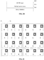
- Fig. 2A schematically illustrates an arrangement style of pixel units of the array substrate 110. As shown in Fig. 2 , this area may include 4*4 pixel units (namely 16 pixel units). Each pixel unit may include 3 subpixel units 20. 16 pixel units may include 48 subpixel units. The subpixel units 20 may include respective Thin Film Transistor (TFT) areas 22 and transparent electrode areas 24.
- TFT Thin Film Transistor
- Fig 2A only illustrates a local area of the array substrate 110.
- the array substrate 110 may be consisted of a plurality of areas shown by Fig 2A .
- the arrangement style shown in Fig 2A is illustrative only, and is not intended to limit the present disclosure.
- the position of the optical sensor array may have two different cases according to the structure of the OLED panel.
- the optical sensor array may include a*b optical sensors, and each optical sensor may be disposed in the TFT area of a corresponding subpixel unit.
- a ⁇ m, b ⁇ n, and a and b may be positive integers.
- each TFT area 26 may have a corresponding optical sensor 25.
- the optical sensors may correspond to a portion of the subpixel units of the array substrate.
- Fig. 3A is a structure diagram illustrating an image display panel.
- the LCD panel may include a backlight 310, a first polaroid 320 above the backlight 310, an array substrate 330 above the first polaroid 320, a liquid crystal layer 340 above the array substrate 330, a color filter layer 350 above the liquid crystal layer 340, and a second polaroid 360 above the color filter layer 350.
- the backlight 310 may be configured to provide backlight for the LCD panel.
- the backlight 310 may include, but not limit to, anyone of an Electro Luminescent (EL), a Cold Cathode Fluorescent Lamp (CCFL), and a Light Emitting Diode (LED).
- EL Electro Luminescent
- CCFL Cold Cathode Fluorescent Lamp
- LED Light Emitting Diode
- the first polaroid 320 and the second polaroid 360 may be used to allow light in a certain direction to pass through.
- the optically transparent axis of the first polaroid 320 and the optically transparent axis of the second polaroid 360 may be orthogonal.
- the array substrate 330 may include x*n pixel units, and each pixel unit may include y subpixel units.
- the pixel unit may include 3 subpixel units, which are R subpixel unit, G subpixel unit, and B subpixel unit.
- the pixel unit may include 4 subpixel units, which are R subpixel unit, G subpixel unit, B subpixel unit, and W subpixel unit.
- the value of y may be 3 or 4.
- the arrangement style of pixel units of the array substrate 330 may be shown by Fig. 2A , which will not be described again.
- the backlight provided by the backlight 310 may be able to pass through the transparent electrode areas 24 and cannot pass through the TFT areas 22.
- Liquid crystal molecules of the liquid crystal layer 340 may be controlled by the TFT areas 22 of the array substrate 330 to perform rotation. Different amount of light may be allowed to pass through based on the different rotation angle, such that the display gray scales of the pixel units may be formed.
- the color filter layer 350 may allow the LCD panel to present colorful pictures.
- the color filter layer 350 may include three different colors (e.g., R, G, B) of filter areas arranged in an array.
- One filter area may correspond to one subpixel unit of the array substrate 330.
- the light generated by the backlight 310 may pass down-up through the first polaroid 320, the transparent electrode areas of the array substrate 330, the liquid crystal layer 340, the color filter layer 350, and the second polaroid 360.
- the voltage generated by the array substrate 330 may control the rotation of the liquid crystal molecules of the liquid crystal layer 340.
- the liquid crystal layer 340 may change the brightness of the light by rotating the liquid crystal molecules, such that the different subpixel units corresponding to three different colors (R, G, B) of the color filter layer 350 may generate different gray scales. Accordingly, the display of an image may be implemented.
- the position of the optical sensor array may have three different cases according to the structure of the LCD panel.
- the optical sensor array may include a*b optical sensors, and each optical sensor may be disposed in the TFT area of a corresponding subpixel unit.
- a ⁇ m, b ⁇ n, and a and b may be positive integers.
- each TFT area 26 may have a corresponding optical sensor 25.
- the optical sensors may correspond to a portion of the subpixel units of the array substrate.
- Fig. 4 is a structure diagram illustrating a display panel according to an embodiment of the present disclosure.
- the display panel may be a display panel of an electronic device such as a cellphone, a tablet computer, a laptop and the like.
- the display panel may include: an image display panel (not shown); an optical sensor array 410 in the image display panel, wherein the optical sensor array 410 may include a plurality of optical sensors arranged in an array; and a grating panel 420 above the optical sensor array 410, wherein the grating panel 420 has an optical shading area which is not overlapped with an optical sensing area of the optical sensors.
- the optical shading area of the grating panel is not overlapped with the optical sensing area of the optical sensors.
- the optical shading area of the grating panel and the optical sensing area of the optical sensors may be complementary.
- the area which is not shaded by the optical shading area of the grating panel may be the optical sensing area of the optical sensors.
- the optical sensing area of the optical sensors is not the optical shading area of the grating panel.
- the optical sensing area of the optical sensors and the optical shading area of the grating panel may supplement each other.
- the optical sensing area of the optical sensors adding the optical shading area of the grating panel may be the display area of the display panel.
- Fig. 5 is a diagram illustrating a display area of a display panel.
- the blank portion may be the optical sensing area 51 of the optical sensors.
- the black portion may be the optical shading area 52 of the grating panel.
- the optical sensing area 51 of the optical sensors adding the optical shading area 52 of the grating panel may be the display area of the display panel.
- Fig 5 only illustrates a local area of the display area of the display panel.
- the display area may be consisted of a plurality of areas shown by Fig 5 .
- the display area shown in Fig 5 is illustrative only, and is not intended to limit the present disclosure.
- the grating panel may be disposed above the optical sensor array. Because the optical shading area of the grating panel is not overlapped with the optical sensing area of the optical sensors, the optical shading area makes the area outside the optical sensing area to be light-tight.
- the optical shading area may prevent light diagonally against the optical sensors from passing through and allow light perpendicular to the optical sensors to pass through so as to reduce light that is not the light perpendicular to the optical sensors. Accordingly, the contrast ratio and saturability of the images collected by the optical sensors may be improved, such that the quality of the images can be guaranteed.
- the image display panel may be an OLED panel.
- the optical sensor array may be disposed on a same layer as the array substrate or may be disposed between the array substrate and the OLED layer.
- the position of the grating panel in the display panel may have two different cases.
- the optical shading area of the grating panel is overlapped with the transparent electrode areas.
- the optical shading area is not overlapped with the TFT areas.
- the optical shading area of the grating panel is completely overlapped with the transparent electrode areas.
- the black area 61 may be the optical shading area.
- the transparent electrode areas may be under the optical shading area.
- the optical shading area is not overlapped with the optical sensing area 62 of the optical sensors.
- the optical sensing area 62 may be the TFT areas. Each TFT area may be disposed with an optical sensor 65.
- the optical shading area of the grating panel is overlapped with a portion of the transparent electrode areas.
- the black area 63 may be the optical shading area.
- the transparent electrode areas may be under the optical shading area 63.
- the optical shading area 63 is overlapped with a portion of the transparent electrode areas.
- the optical shading area 63 is not overlapped with the optical sensing area 64 of the optical sensors.
- the image display panel may be a LCD panel.
- the position of the grating panel in the display panel may have a connection with the position of the optical sensor array.
- the optical shading area of the grating panel is overlapped with the transparent electrode areas.
- the optical shading area is not overlapped with the TFT areas.
- the optical shading area of the grating panel is completely overlapped with the transparent electrode areas.
- the optical shading area of the grating panel is overlapped with a portion of the transparent electrode areas.
- the grating panel may be a solid structure.
- the grating panel may include an optical shading area and an optically transparent area.
- the optical shading area and the optically transparent area of the grating panel may not change based on the operation condition of the optical sensors.
- the optical shading area may be overlapped with the transparent electrode areas.
- the area 61 may be the optical shading area of the grating panel.
- the area 62 may be the optically transparent area of the grating panel.
- the grating panel may be a solid structure. Namely, the position and transmittance of the optical shading area and the optically transparent area of the grating panel may not change.
- the transmittance of the optical shading area of the grating panel should not larger than a predetermined value which may be determined according to practical situations.
- the grating panel may be transparent or semitransparent with a certain thickness.
- the grating panel with a solid structure may not only shade light toward the display panel but also shade light out from the display panel, which may affect the display effect of images during displaying the images. Accordingly, the grating panel with a solid structure may be used in a display panel which has a lower requirement in transmittance.
- the grating panel may be a dynamic structure.
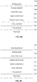
- the grating panel may include a lower polaroid 910, a liquid crystal grating layer 920 above the lower polaroid, and a upper polaroid 930 above the liquid crystal grating layer 920.
- the liquid crystal grating layer comprises a liquid crystal area and an optically transparent area.
- the liquid crystal state of the liquid crystal area may change based on the operation condition of the optical sensors.
- the liquid crystal area is overlapped with the transparent electrode areas.
- the area 61 may be the liquid crystal area of the grating panel.
- the area 62 may be the optically transparent area of the grating panel.
- the transparent electrode areas may be disposed under the liquid crystal area 61.
- the grating panel may be a dynamic structure. As shown in Fig. 9B , the grating panel may include a liquid crystal grating layer 920 above a second polaroid 940, and a upper polaroid 930 above the liquid crystal grating layer 920.
- the area 61 may be the liquid crystal area of the grating panel.
- the area 62 may be the optically transparent area of the grating panel.
- the transparent electrode areas may be disposed under the liquid crystal area 61.
- the grating panel may be a dynamic structure.
- the grating panel may include a liquid crystal grating layer 920 under a second polaroid 940, and a upper polaroid 950 under the liquid crystal grating layer 920.
- the liquid crystal grating layer comprises a liquid crystal area and an optically transparent area.
- the liquid crystal state of the liquid crystal area may change based on the operation condition of the optical sensors.
- the liquid crystal area is overlapped with the transparent electrode areas.
- the area 61 may be the liquid crystal area of the grating panel.
- the area 62 may be the optically transparent area of the grating panel.
- the transparent electrode areas may be disposed under the liquid crystal area 61.
- the display panel may include a liquid crystal grating control circuitry connected with the liquid crystal grating of the grating panel.
- the liquid crystal grating control circuitry may be configured to control the state of the liquid crystal area of the liquid crystal grating layer of the grating panel.
- the liquid crystal grating control circuitry may include two electrodes.
- One electrode may be used to control the state of liquid crystals in horizontal direction of the liquid crystal area.
- Another electrode may be used to control the state of liquid crystals in vertical direction of the liquid crystal area.
- the liquid crystal grating control circuitry may include one electrode.
- the electrode may be used to control the state of liquid crystals in horizontal direction and liquid crystals in vertical direction of the liquid crystal area.
- Fig. 10 is a block diagram illustrating a terminal according to an exemplary embodiment of the present disclosure.
- the terminal 1000 may include a display panel 1010, a memory 1020, a processing component 1030, a power component 1040, an audio component 1050, and an input/output (I/O) interface 1060.
- a display panel 1010 the terminal 1000 may include a display panel 1010, a memory 1020, a processing component 1030, a power component 1040, an audio component 1050, and an input/output (I/O) interface 1060.
- I/O input/output
- the display panel 1010 may be a display panel illustrated by anyone of Fig. 4 , 6A , 6B , 7A , 7B, 7C , 7D, 7E , 7F, 8A , 8B, 8C , or 8D according to above embodiments.
- the display panel 1010 may include an image display panel 1011 and a grating panel 1012 with a solid structure.
- the image display panel 1011 may include an optical sensor array (not shown).
- the memory 1020 is configured to store various types of data to support the operation of the device 1000. Examples of such data include instructions for any applications or methods operated on the device 1000, contact data, phonebook data, messages, pictures, video, etc.
- the memory 1020 may be implemented using any type of volatile or non-volatile memory devices, or a combination thereof, such as a static random access memory (SRAM), an electrically erasable programmable read-only memory (EEPROM), an erasable programmable read-only memory (EPROM), a programmable read-only memory (PROM), a read-only memory (ROM), a magnetic memory, a flash memory, a magnetic or optical disk.
- SRAM static random access memory
- EEPROM electrically erasable programmable read-only memory
- EPROM erasable programmable read-only memory
- PROM programmable read-only memory
- ROM read-only memory
- magnetic memory a magnetic memory
- flash memory a flash memory
- magnetic or optical disk a magnetic or optical
- the processing component 1030 typically controls overall operations of the device 1000, such as the operations associated with display, telephone calls, data communications, camera operations, and recording operations.
- the processing component 1030 may include one or more processors to execute instructions to perform all or part of the steps in the above described methods.
- the processing component 1030 may include one or more modules which facilitate the interaction between the processing component 1030 and other components.
- the power component 1040 provides power to various components of the device 1000.
- the power component 1040 may include a power management system, one or more power sources, and any other components associated with the generation, management, and distribution of power in the device 1000.
- the audio component 1050 is configured to output and/or input audio signals.
- the audio component 1050 includes a microphone ("MIC") configured to receive an external audio signal when the device 1000 is in an operation mode, such as a call mode, a recording mode and a voice recognition mode.
- the received audio signal may be further stored in the memory.
- the audio component 1050 further includes a speaker to output audio signals.
- the I/O interface 1060 provides an interface between the processing component 1030 and peripheral interface modules, such as a keyboard, a click wheel, buttons, and the like.
- the buttons may include, but are not limited to, a home button, a volume button, a starting button, and a locking button.
- Fig. 11 is a block diagram illustrating a terminal according to an exemplary embodiment.
- the terminal 1100 may include a display panel 1110, a memory 1120, a processing component 1130, a power component 1140, an audio component 1150, and an input/output (I/O) interface 1160.
- a display panel 1110 the terminal 1100 may include a display panel 1110, a memory 1120, a processing component 1130, a power component 1140, an audio component 1150, and an input/output (I/O) interface 1160.
- I/O input/output
- the display panel 1110 may be a display panel illustrated by anyone of Fig. 4 , 6A , 6B , 7A , 7B, 7C , 7D, 7E , 7F, 8A , 8B, 8C , or 8D according to above embodiments.
- the display panel 1110 may include an image display panel 1111, a grating panel 1112 with a dynamic structure, and a liquid crystal grating control circuitry 1113 connected with the liquid crystal grating (not shown) of the grating panel 1112.
- the image display panel 1111 may include an optical sensor array (not shown).
- the memory 1120 is configured to store various types of data to support the operation of the device 1100. Examples of such data include instructions for any applications or methods operated on the device 1100, contact data, phonebook data, messages, pictures, video, etc.
- the memory 1120 may be implemented using any type of volatile or non-volatile memory devices, or a combination thereof, such as a static random access memory (SRAM), an electrically erasable programmable read-only memory (EEPROM), an erasable programmable read-only memory (EPROM), a programmable read-only memory (PROM), a read-only memory (ROM), a magnetic memory, a flash memory, a magnetic or optical disk.
- SRAM static random access memory
- EEPROM electrically erasable programmable read-only memory
- EPROM erasable programmable read-only memory
- PROM programmable read-only memory
- ROM read-only memory
- magnetic memory a magnetic memory
- flash memory a flash memory
- magnetic or optical disk a magnetic
- the processing component 1130 typically controls overall operations of the device 1100, such as the operations associated with display, telephone calls, data communications, camera operations, and recording operations.
- the processing component 1130 may include one or more processors to execute instructions to perform all or part of the steps in the above described methods.
- the processing component 1130 may include one or more modules which facilitate the interaction between the processing component 1130 and other components.
- the power component 1140 provides power to various components of the device 1100.
- the power component 1140 may include a power management system, one or more power sources, and any other components associated with the generation, management, and distribution of power in the device 1100.
- the audio component 1150 is configured to output and/or input audio signals.
- the audio component 1150 includes a microphone ("MIC") configured to receive an external audio signal when the device 1100 is in an operation mode, such as a call mode, a recording mode and a voice recognition mode.
- the received audio signal may be further stored in the memory.
- the audio component 1150 further includes a speaker to output audio signals.
- the I/O interface 1160 provides an interface between the processing component 1130 and peripheral interface modules, such as a keyboard, a click wheel, buttons, and the like.
- the buttons may include, but are not limited to, a home button, a volume button, a starting button, and a locking button.
- the embodiment of the present disclosure provides a method for display control.
- the embodiment illustrates the method for display control applied in a terminal, which includes a grating panel illustrated by Fig. 9A, 9B , or 9C in the display panel.
- the liquid crystals of the liquid crystal grating layer of the grating panel may be controlled, by the liquid crystal grating control circuitry, to convert from an optically transparent state to an optical shading state during the optical sensor array is in operation.
- the optically transparent state may be a state that light can completely pass through.
- the optical shading state may be a state that light cannot pass through or the transmittance is less than a predetermined value.
- the predetermined value may be a value that is predetermined.
- the liquid crystal grating layer of the grating panel may be in the optically transparent state during the optical sensor array is not in operation.
- the terminal may control, by the liquid crystal grating control circuitry, the liquid crystal grating layer of the grating panel to convert from the optically transparent state to the optical shading state and the liquid crystal grating layer to stay in this state.
- the case that the optical sensor array is in operation may be that the terminal collects images by the optical sensors.
- the light that is not in vertical direction should be shaded. Accordingly, the liquid crystal grating layer of the liquid crystal grating panel should be in the optical shading state.
- the case that the optical sensor array is not in operation may be that the terminal does not collect images by the optical sensors.
- the image display panel may desire to display images. If the liquid crystal grating layer of the liquid crystal grating panel is in the optically transparent state, the images displayed by the image display panel may be shaded. Accordingly, in order not to affect the image display during the optical sensors are not in operation, the liquid crystal grating layer should be in the optically transparent state.
Landscapes
- Physics & Mathematics (AREA)
- Nonlinear Science (AREA)
- Chemical & Material Sciences (AREA)
- General Physics & Mathematics (AREA)
- Crystallography & Structural Chemistry (AREA)
- Mathematical Physics (AREA)
- Optics & Photonics (AREA)
- Engineering & Computer Science (AREA)
- Theoretical Computer Science (AREA)
- Computer Hardware Design (AREA)
- Electromagnetism (AREA)
- Inorganic Chemistry (AREA)
- Devices For Indicating Variable Information By Combining Individual Elements (AREA)
- Life Sciences & Earth Sciences (AREA)
- Sustainable Development (AREA)
- Electroluminescent Light Sources (AREA)
- Liquid Crystal (AREA)
- Control Of Indicators Other Than Cathode Ray Tubes (AREA)
- Studio Devices (AREA)
- Liquid Crystal Display Device Control (AREA)
- Transforming Light Signals Into Electric Signals (AREA)
- Color Television Image Signal Generators (AREA)
- Control Of El Displays (AREA)
Abstract
Description
- The present disclosure generally relates to the technical field of displays, and more particularly to a display panel, terminal, and method for display control.
- A camera may be a common infrastructure component of a mobile terminal. The camera may be used for collecting images.
- In related art, optical sensors for collecting images may be disposed on a display panel of the mobile terminal, and may be a substitute for the camera mounted in a pinhole disposed on a frame area of the mobile terminal.
- In order to solve the problems that images collected by the optical sensors for collecting images in the display panel of the mobile terminal have bad contrast ratio, bad saturability, and bad display quality, the present disclosure provides a display panel, terminal, and method for display control. The technical solutions are as follows.
- According to a first aspect of the present disclosure, a display panel is provided. The display panel may include: an image display panel; an optical sensor array in the image display panel, wherein the optical sensor array may include a plurality of optical sensors arranged in an array; and a grating panel above the optical sensor array, wherein the grating panel has an optical shading area which is not overlapped with an optical sensing area of the optical sensors.
- As used herein, the term "above" refers to the relative position of a component within the display panel. A component that is "above" another means that the component is "on top of", or otherwise displaced in the direction of travel of light emitted from the display panel.
- In an optional embodiment, the image display panel may include an array substrate and an Organic Light Emitting Display (OLED) layer above the array substrate; the optical sensor array is disposed on a same layer as the array substrate, or the optical sensor array is disposed between the array substrate and the OLED layer; wherein the array substrate may include m*n subpixel units, and the subpixel units may include respective transparent electrode areas and Thin Film Transistor (TFT) areas; the optical sensor array may include a*b optical sensors, and each optical sensor is disposed in the TFT area of a corresponding subpixel unit; and wherein, a≤m, b≤n.
- In an optional embodiment, in the case that the optical sensor array is disposed on a same layer as the array substrate or is disposed between the array substrate and the OLED layer, the grating panel is disposed between the array substrate and the OLED layer or above the OLED layer; wherein the optical shading area of the grating panel is overlapped with the transparent electrode areas.
- In an optional embodiment, the image display panel may include a backlight, an array substrate above the backlight, a liquid crystal layer above the array substrate, a color filter layer above the liquid crystal, and a polaroid above the color filter layer; the optical sensor array is disposed on a same layer as the array substrate; or the optical sensor array is disposed between the array substrate and the liquid crystal layer; or the optical sensor array is disposed between the liquid crystal layer and the color filter layer; wherein the array substrate may include m*n subpixel units, and the subpixel units may include respective transparent electrode areas and Thin Film Transistor (TFT) areas; the optical sensor array may include a*b optical sensors, and each optical sensor is disposed in the TFT area of a corresponding subpixel unit; and wherein, a≤m, b≤n.
- In an optional embodiment, in the case that the optical sensor array is disposed on a same layer as the array substrate, the grating panel is disposed above the array substrate; in the case that the optical sensor array is disposed between the array substrate and the liquid crystal layer, the grating panel is disposed between the optical sensor array and the liquid crystal layer or above the liquid crystal layer; in the case that the optical sensor array is disposed between the liquid crystal layer and the color filter layer, the grating panel is disposed between the optical sensor array and the color filter layer or above the color filter layer; wherein the optical shading area of the grating panel is overlapped with the transparent electrode areas.
- In an optional embodiment, the grating panel may include the optical shading area and an optically transparent area, and the optical shading area is overlapped with the transparent electrode areas.
- In an optional embodiment, the grating panel may include a lower polaroid, a liquid crystal grating layer above the lower polaroid, and a upper polaroid above the liquid crystal grating layer; wherein the liquid crystal grating layer may include a liquid crystal area and an optically transparent area, and the liquid crystal area is overlapped with the transparent electrode areas.
- In an optional embodiment, the grating panel is disposed above the polaroid of the image display panel, and may include a liquid crystal grating layer and a upper polaroid above the liquid crystal grating layer; or the grating panel is disposed between the color filter layer and the polaroid, and may include a liquid crystal grating layer below the polaroid and a lower polaroid below the liquid crystal grating layer; wherein the liquid crystal grating layer may include a liquid crystal area and an optically transparent area, and the liquid crystal area is overlapped with the transparent electrode areas.
- In an optional embodiment, the display panel may further include a liquid crystal grating control circuitry connected with the liquid crystal grating layer.
- According to a second aspect of the present disclosure, a terminal is provided. The terminal may include the display panel according to the first aspect of the present disclosure.
- According to a third aspect of the present disclosure, a method for display control in a terminal including the display panel according to the first aspect of the present disclosure is provided. The method may include: controlling, by the liquid crystal grating control circuitry, the liquid crystal grating layer of the grating panel to convert from an optically transparent state to an optical shading state during the optical sensor array is in operation.
- In the present disclosure, the grating panel may be disposed above the optical sensor array. Because the optical shading area of the grating panel is not overlapped with the optical sensing area of the optical sensors, the optical shading area makes the area outside the optical sensing area to be light-tight. The optical shading area may prevent light diagonally against the optical sensors from passing through and allow light perpendicular to the optical sensors to pass through so as to reduce light that is not the light perpendicular to the optical sensors. Accordingly, the contrast ratio and saturability of the images collected by the optical sensors may be improved, such that the quality of the images can be guaranteed.
- In order to explain the technical solution of the embodiments of the present disclosure, the accompanying drawings incorporated in the detail description will be introduced in the followings. Obviously, the accompanying drawings described hereinafter are merely exemplary embodiments of the present disclosure, and an ordinary person skilled in the art may obtain other accompanying drawings according to these accompanying drawings without creative work.
-
Fig. 1 is a structure diagram illustrating an image display panel according to an embodiment of the present disclosure. -
Fig. 2A is a diagram illustrating an arrangement style of pixel units of an array substrate. -
Fig. 2B is a structure diagram illustrating an image display panel according to an embodiment of the present disclosure. -
Fig. 2C is a diagram illustrating a position of an optical sensor according to an exemplary embodiment. -
Fig. 3A is a structure diagram illustrating an image display panel according to an embodiment of the present disclosure. -
Fig. 3B is a structure diagram illustrating an image display panel according to an embodiment of the present disclosure. -
Fig. 3C is a structure diagram illustrating an image display panel according to an embodiment of the present disclosure. -
Fig. 4 is a structure diagram illustrating a display panel according to an embodiment of the present disclosure. -
Fig. 5 is a diagram illustrating a display area of a display panel according to an embodiment of the present disclosure. -
Fig. 6A is a structure diagram illustrating a display panel according to an embodiment of the present disclosure. -
Fig. 6B is a structure diagram illustrating a display panel according to an embodiment of the present disclosure. -
Fig. 6C is a diagram illustrating a display area of a display panel according to an embodiment of the present disclosure. -
Fig. 6D is a diagram illustrating a display area of a display panel according to an embodiment of the present disclosure. -
Fig. 7A is a structure diagram illustrating a display panel according to an embodiment of the present disclosure. -
Fig. 7B is a structure diagram illustrating a display panel according to an embodiment of the present disclosure. -
Fig. 7C is a structure diagram illustrating a display panel according to an embodiment of the present disclosure. -
Fig. 7D is a structure diagram illustrating a display panel according to an embodiment of the present disclosure. -
Fig. 7E is a structure diagram illustrating a display panel according to an embodiment of the present disclosure. -
Fig. 7F is a structure diagram illustrating a display panel according to an embodiment of the present disclosure. -
Fig. 8A is a structure diagram illustrating a display panel according to an embodiment of the present disclosure. -
Fig. 8B is a structure diagram illustrating a display panel according to an embodiment of the present disclosure. -
Fig. 8C is a structure diagram illustrating a display panel according to an embodiment of the present disclosure. -
Fig. 8D is a structure diagram illustrating a display panel according to an embodiment of the present disclosure. -
Fig. 9A is a structure diagram illustrating a grating panel according to an embodiment of the present disclosure. -
Fig. 9B is a structure diagram illustrating a grating panel according to an embodiment of the present disclosure. -
Fig. 9C is a structure diagram illustrating a grating panel according to an embodiment of the present disclosure. -
Fig. 10 is a block diagram illustrating a terminal according to an exemplary embodiment. -
Fig. 11 is a block diagram illustrating a terminal according to an exemplary embodiment. - Reference will now be made in detail to example embodiments, examples of which are illustrated in the accompanying drawings. The following description refers to the accompanying drawings in which same numbers in different drawings represent same or similar elements unless otherwise described. The implementations set forth in the following description of example embodiments do not represent all implementations consistent with the present disclosure. Instead, they are merely examples of devices and methods consistent with aspects related to the present disclosure as recited in the appended claims.
- Two image display panels may be introduced before introducing and illustrating embodiments of the present disclosure. The two image display panels are Organic Light Emitting Display (OLED) panel and Liquid Crystal Display (LCD) panel.
- Referring to
Fig. 1, Fig. 1 is a structure diagram illustrating an OLED panel. As shown inFig. 1 , the OLED panel may include anarray substrate 110 and anOLED layer 120 above thearray substrate 110. - The
OLED layer 120 may include x*n pixel units, and each pixel unit may include y subpixel units. Namely, the OLED layer may include m*n subpixel units, wherein m=x*y. Usually, the pixel unit may include 3 subpixel units, which are Red (R) subpixel unit, Green (G) subpixel unit, and Blue (B) subpixel unit. In some embodiments, the pixel unit may include 4 subpixel units, which are Red (R) subpixel unit, Green (G) subpixel unit, Blue (B) subpixel unit, and White (W) subpixel unit. Namely, the value of y may be 3 or 4. Wherein, m, n, x, and y may be positive integers. - Accordingly, the
array substrate 110 may include m*n subpixel units corresponding to the subpixel units of theOLED layer 120. - The
array substrate 110 may provide a driving electric field for theOLED layer 120. Organic semiconductor materials and luminescent materials in theOLED layer 120 may be driven by the electric field to irradiate, such that the display of an image may be implemented. -
Fig. 2A schematically illustrates an arrangement style of pixel units of thearray substrate 110. As shown inFig. 2 , this area may include 4*4 pixel units (namely 16 pixel units). Each pixel unit may include 3subpixel units 20. 16 pixel units may include 48 subpixel units. Thesubpixel units 20 may include respective Thin Film Transistor (TFT)areas 22 andtransparent electrode areas 24. - It should be noted that,
Fig 2A only illustrates a local area of thearray substrate 110. Thearray substrate 110 may be consisted of a plurality of areas shown byFig 2A . The arrangement style shown inFig 2A is illustrative only, and is not intended to limit the present disclosure. - The position of the optical sensor array may have two different cases according to the structure of the OLED panel.
- 1. The optical sensor array may be disposed on the same layer as the
array substrate 110. - 2. The
optical sensor array 130 may be disposed between thearray substrate 110 and theOLED layer 120, as shown inFig 2B . - Wherein, the optical sensor array may include a*b optical sensors, and each optical sensor may be disposed in the TFT area of a corresponding subpixel unit. Wherein, a≤m, b≤n, and a and b may be positive integers.
- In the case that the number of the optical sensors is equal to the number of the subpixel units of the array substrate (namely, a=K*m, b=n, wherein K=1), one optical sensor in the optical sensor array may correspond to one subpixel unit in the array substrate, namely each subpixel unit may have a corresponding optical sensor. As shown in
Fig. 2C , eachTFT area 26 may have a correspondingoptical sensor 25. - In the case that the number of the optical sensors is less than the number of the subpixel units of the array substrate (namely a<K*m, b<n, or a<K*m, b=n, or a=K*m, b<n, wherein K=1), the optical sensors may correspond to a portion of the subpixel units of the array substrate.
- Referring to
Fig. 3A, Fig. 3A is a structure diagram illustrating an image display panel. As shown inFig. 3A , the LCD panel may include abacklight 310, afirst polaroid 320 above thebacklight 310, anarray substrate 330 above thefirst polaroid 320, aliquid crystal layer 340 above thearray substrate 330, acolor filter layer 350 above theliquid crystal layer 340, and asecond polaroid 360 above thecolor filter layer 350. - The
backlight 310 may be configured to provide backlight for the LCD panel. Thebacklight 310 may include, but not limit to, anyone of an Electro Luminescent (EL), a Cold Cathode Fluorescent Lamp (CCFL), and a Light Emitting Diode (LED). - The
first polaroid 320 and thesecond polaroid 360 may be used to allow light in a certain direction to pass through. The optically transparent axis of thefirst polaroid 320 and the optically transparent axis of thesecond polaroid 360 may be orthogonal. - The
array substrate 330 may include x*n pixel units, and each pixel unit may include y subpixel units. Namely, the OLED layer may include m*n subpixel units, wherein m=x*y. Usually, the pixel unit may include 3 subpixel units, which are R subpixel unit, G subpixel unit, and B subpixel unit. In some embodiments, the pixel unit may include 4 subpixel units, which are R subpixel unit, G subpixel unit, B subpixel unit, and W subpixel unit. Namely, the value of y may be 3 or 4. - The arrangement style of pixel units of the
array substrate 330 may be shown byFig. 2A , which will not be described again. The backlight provided by thebacklight 310 may be able to pass through thetransparent electrode areas 24 and cannot pass through theTFT areas 22. - Liquid crystal molecules of the
liquid crystal layer 340 may be controlled by theTFT areas 22 of thearray substrate 330 to perform rotation. Different amount of light may be allowed to pass through based on the different rotation angle, such that the display gray scales of the pixel units may be formed. - The
color filter layer 350 may allow the LCD panel to present colorful pictures. Thecolor filter layer 350 may include three different colors (e.g., R, G, B) of filter areas arranged in an array. One filter area may correspond to one subpixel unit of thearray substrate 330. - The light generated by the
backlight 310 may pass down-up through thefirst polaroid 320, the transparent electrode areas of thearray substrate 330, theliquid crystal layer 340, thecolor filter layer 350, and thesecond polaroid 360. The voltage generated by thearray substrate 330 may control the rotation of the liquid crystal molecules of theliquid crystal layer 340. Theliquid crystal layer 340 may change the brightness of the light by rotating the liquid crystal molecules, such that the different subpixel units corresponding to three different colors (R, G, B) of thecolor filter layer 350 may generate different gray scales. Accordingly, the display of an image may be implemented. - The position of the optical sensor array may have three different cases according to the structure of the LCD panel.
- 1. The optical sensor array may be disposed on the same layer as the array substrate.
- 2. The
optical sensor array 370 may be disposed between thearray substrate 330 and theliquid crystal layer 340, as shown inFig 3B . - 3. The
optical sensor array 370 may be disposed between theliquid crystal layer 340 and thecolor filter layer 350, as shown inFig 3C . - Wherein, the optical sensor array may include a*b optical sensors, and each optical sensor may be disposed in the TFT area of a corresponding subpixel unit. Wherein, a≤m, b≤n, and a and b may be positive integers.
- In the case that the number of the optical sensors is equal to the number of the subpixel units of the array substrate (namely, a=K*m, b=n, wherein K=1), one optical sensor in the optical sensor array may correspond to one subpixel unit in the array substrate, namely each subpixel unit may have a corresponding optical sensor. As shown in
Fig. 2C , eachTFT area 26 may have a correspondingoptical sensor 25. - In the case that the number of the optical sensors is less than the number of the subpixel units of the array substrate (namely a<K*m, b<n, or a<K*m, b=n, or a=K*m, b<n, wherein K=1), the optical sensors may correspond to a portion of the subpixel units of the array substrate.
-
Fig. 4 is a structure diagram illustrating a display panel according to an embodiment of the present disclosure. The display panel may be a display panel of an electronic device such as a cellphone, a tablet computer, a laptop and the like. As shown inFig. 4 , the display panel may include: an image display panel (not shown); anoptical sensor array 410 in the image display panel, wherein theoptical sensor array 410 may include a plurality of optical sensors arranged in an array; and agrating panel 420 above theoptical sensor array 410, wherein thegrating panel 420 has an optical shading area which is not overlapped with an optical sensing area of the optical sensors. - The optical shading area of the grating panel is not overlapped with the optical sensing area of the optical sensors. Namely, the optical shading area of the grating panel and the optical sensing area of the optical sensors may be complementary. The area which is not shaded by the optical shading area of the grating panel may be the optical sensing area of the optical sensors. The optical sensing area of the optical sensors is not the optical shading area of the grating panel. The optical sensing area of the optical sensors and the optical shading area of the grating panel may supplement each other. The optical sensing area of the optical sensors adding the optical shading area of the grating panel may be the display area of the display panel.
-
Fig. 5 is a diagram illustrating a display area of a display panel. The blank portion may be theoptical sensing area 51 of the optical sensors. The black portion may be theoptical shading area 52 of the grating panel. Theoptical sensing area 51 of the optical sensors adding theoptical shading area 52 of the grating panel may be the display area of the display panel. - It should be noted that,
Fig 5 only illustrates a local area of the display area of the display panel. The display area may be consisted of a plurality of areas shown byFig 5 . The display area shown inFig 5 is illustrative only, and is not intended to limit the present disclosure. - Above all, in the display panel according to an embodiment of the present disclosure, the grating panel may be disposed above the optical sensor array. Because the optical shading area of the grating panel is not overlapped with the optical sensing area of the optical sensors, the optical shading area makes the area outside the optical sensing area to be light-tight. The optical shading area may prevent light diagonally against the optical sensors from passing through and allow light perpendicular to the optical sensors to pass through so as to reduce light that is not the light perpendicular to the optical sensors. Accordingly, the contrast ratio and saturability of the images collected by the optical sensors may be improved, such that the quality of the images can be guaranteed.
- In a possible embodiment, the image display panel may be an OLED panel. The optical sensor array may be disposed on a same layer as the array substrate or may be disposed between the array substrate and the OLED layer. The position of the grating panel in the display panel may have two different cases.
- 1. The grating panel may be disposed between the array substrate and the OLED layer. As shown in
Fig. 6A , thegrating panel 610 may be disposed between thearray substrate 110 and theOLED layer 120. - 2. The grating panel may be disposed above the OLED layer. As shown in
Fig. 6A , thegrating panel 610 may be disposed above theOLED layer 120. - Wherein, the optical shading area of the grating panel is overlapped with the transparent electrode areas. The optical shading area is not overlapped with the TFT areas.
- Optionally, the optical shading area of the grating panel is completely overlapped with the transparent electrode areas. As shown in
Fig. 6C , theblack area 61 may be the optical shading area. The transparent electrode areas may be under the optical shading area. The optical shading area is not overlapped with theoptical sensing area 62 of the optical sensors. Theoptical sensing area 62 may be the TFT areas. Each TFT area may be disposed with anoptical sensor 65. - Optionally, the optical shading area of the grating panel is overlapped with a portion of the transparent electrode areas. As shown in
Fig. 6D , theblack area 63 may be the optical shading area. The transparent electrode areas may be under theoptical shading area 63. Theoptical shading area 63 is overlapped with a portion of the transparent electrode areas. Theoptical shading area 63 is not overlapped with theoptical sensing area 64 of the optical sensors. - In a possible embodiment, the image display panel may be a LCD panel. The position of the grating panel in the display panel may have a connection with the position of the optical sensor array.
- 1. The optical sensor array is disposed on a same layer as the array substrate. The position of the grating panel in the display panel may have four different cases.
- 1). The grating panel may be disposed between the array substrate and the liquid crystal layer. As shown in
Fig. 7A , thegrating panel 710 may be disposed between thearray substrate 330 and theliquid crystal layer 340. - 2). The grating panel may be disposed between the liquid crystal layer and the color filter layer. As shown in
Fig. 7B , thegrating panel 710 may be disposed between theliquid crystal layer 340 and thecolor filter layer 350. - 3). The grating panel may be disposed between the color filter layer and the second polaroid. As shown in
Fig. 7C , thegrating panel 710 may be disposed between thecolor filter layer 350 and thesecond polaroid 360. - 4). The grating panel may be disposed above the second polaroid. As shown in
Fig. 7D , thegrating panel 710 may be disposed above thesecond polaroid 360. - 2. The optical sensor array is disposed between the array substrate and the liquid crystal layer. The position of the grating panel in the display panel may have four different cases.
- 1). The grating panel may be disposed between the optical sensor array and the liquid crystal layer. As shown in
Fig. 7E , thegrating panel 710 may be disposed between theoptical sensor array 370 and theliquid crystal layer 340. - 2). The grating panel may be disposed between the liquid crystal layer and the color filter layer. As shown in
Fig. 7F , thegrating panel 710 may be disposed between theliquid crystal layer 340 and thecolor filter layer 350. - 3). The grating panel may be disposed between the color filter layer and the second polaroid. As shown in
Fig. 8A , thegrating panel 710 may be disposed between thecolor filter layer 350 and thesecond polaroid 360. - 4). The grating panel may be disposed above the second polaroid. As shown in
Fig. 8B , thegrating panel 710 may be disposed above thesecond polaroid 360. - 3. The optical sensor array is disposed between the liquid crystal layer and the color filter layer. The position of the grating panel in the display panel may have two different cases.
- 1). The grating panel may be disposed between the color filter layer and the second polaroid. As shown in
Fig. 8C , thegrating panel 710 may be disposed between thecolor filter layer 350 and thesecond polaroid 360. - 2). The grating panel may be disposed above the second polaroid. As shown in
Fig. 8D , thegrating panel 710 may be disposed above thesecond polaroid 360. - Wherein, the optical shading area of the grating panel is overlapped with the transparent electrode areas. The optical shading area is not overlapped with the TFT areas.
- Optionally, the optical shading area of the grating panel is completely overlapped with the transparent electrode areas.
- Optionally, the optical shading area of the grating panel is overlapped with a portion of the transparent electrode areas.
- In the display panel illustrated by
Fig. 4 ,6A ,6B ,7A ,7B, 7C ,7D, 7E ,7F, 8A ,8B, 8C , or8D , the grating panel may be a solid structure. The grating panel may include an optical shading area and an optically transparent area. The optical shading area and the optically transparent area of the grating panel may not change based on the operation condition of the optical sensors. The optical shading area may be overlapped with the transparent electrode areas. As shown inFig. 6C , thearea 61 may be the optical shading area of the grating panel. Thearea 62 may be the optically transparent area of the grating panel. - The grating panel may be a solid structure. Namely, the position and transmittance of the optical shading area and the optically transparent area of the grating panel may not change. In order to guarantee that the display panel is able to display images during the optical sensor array is not in operation, and the optical sensor array is not affected by light that is not in vertical direction during the optical sensor array is collecting images, the transmittance of the optical shading area of the grating panel should not larger than a predetermined value which may be determined according to practical situations.
- Optically, the grating panel may be transparent or semitransparent with a certain thickness.
- The grating panel with a solid structure may not only shade light toward the display panel but also shade light out from the display panel, which may affect the display effect of images during displaying the images. Accordingly, the grating panel with a solid structure may be used in a display panel which has a lower requirement in transmittance.
- In the display panel illustrated by
Fig. 4 ,6A ,6B ,7A ,7B, 7C ,7D, 7E ,7F, 8A ,8B, 8C , or8D , the grating panel may be a dynamic structure. As shown inFig. 9A , the grating panel may include alower polaroid 910, a liquidcrystal grating layer 920 above the lower polaroid, and aupper polaroid 930 above the liquidcrystal grating layer 920. - Wherein, the liquid crystal grating layer comprises a liquid crystal area and an optically transparent area. The liquid crystal state of the liquid crystal area may change based on the operation condition of the optical sensors. The liquid crystal area is overlapped with the transparent electrode areas.
- As shown in
Fig. 6C , thearea 61 may be the liquid crystal area of the grating panel. Thearea 62 may be the optically transparent area of the grating panel. The transparent electrode areas may be disposed under theliquid crystal area 61. - In the display panel illustrated by
Fig. 7D ,8B , or8D , the grating panel may be a dynamic structure. As shown inFig. 9B , the grating panel may include a liquidcrystal grating layer 920 above asecond polaroid 940, and aupper polaroid 930 above the liquidcrystal grating layer 920. - Wherein, the liquid crystal grating layer comprises a liquid crystal area and an optically transparent area. The liquid crystal state of the liquid crystal area may change based on the operation condition of the optical sensors. The liquid crystal area is overlapped with the transparent electrode areas.
- As shown in
Fig. 6C , thearea 61 may be the liquid crystal area of the grating panel. Thearea 62 may be the optically transparent area of the grating panel. The transparent electrode areas may be disposed under theliquid crystal area 61. - In the display panel illustrated by
Fig. 7C ,8A , or8C , the grating panel may be a dynamic structure. As shown inFig. 9C , the grating panel may include a liquidcrystal grating layer 920 under asecond polaroid 940, and aupper polaroid 950 under the liquidcrystal grating layer 920. - Wherein, the liquid crystal grating layer comprises a liquid crystal area and an optically transparent area. The liquid crystal state of the liquid crystal area may change based on the operation condition of the optical sensors. The liquid crystal area is overlapped with the transparent electrode areas.
- As shown in
Fig. 6C , thearea 61 may be the liquid crystal area of the grating panel. Thearea 62 may be the optically transparent area of the grating panel. The transparent electrode areas may be disposed under theliquid crystal area 61. - In the display panel including the grating panel illustrated by
Fig. 9A, 9B , or9C , the display panel may include a liquid crystal grating control circuitry connected with the liquid crystal grating of the grating panel. The liquid crystal grating control circuitry may be configured to control the state of the liquid crystal area of the liquid crystal grating layer of the grating panel. - Optionally, the liquid crystal grating control circuitry may include two electrodes. One electrode may be used to control the state of liquid crystals in horizontal direction of the liquid crystal area. Another electrode may be used to control the state of liquid crystals in vertical direction of the liquid crystal area.
- Optionally, the liquid crystal grating control circuitry may include one electrode. The electrode may be used to control the state of liquid crystals in horizontal direction and liquid crystals in vertical direction of the liquid crystal area.
-
Fig. 10 is a block diagram illustrating a terminal according to an exemplary embodiment of the present disclosure. As shown inFig. 10 , the terminal 1000 may include adisplay panel 1010, amemory 1020, aprocessing component 1030, apower component 1040, anaudio component 1050, and an input/output (I/O)interface 1060. - The
display panel 1010 may be a display panel illustrated by anyone ofFig. 4 ,6A ,6B ,7A ,7B, 7C ,7D, 7E ,7F, 8A ,8B, 8C , or8D according to above embodiments. - The
display panel 1010 may include animage display panel 1011 and agrating panel 1012 with a solid structure. Theimage display panel 1011 may include an optical sensor array (not shown). - The
memory 1020 is configured to store various types of data to support the operation of thedevice 1000. Examples of such data include instructions for any applications or methods operated on thedevice 1000, contact data, phonebook data, messages, pictures, video, etc. Thememory 1020 may be implemented using any type of volatile or non-volatile memory devices, or a combination thereof, such as a static random access memory (SRAM), an electrically erasable programmable read-only memory (EEPROM), an erasable programmable read-only memory (EPROM), a programmable read-only memory (PROM), a read-only memory (ROM), a magnetic memory, a flash memory, a magnetic or optical disk. - The
processing component 1030 typically controls overall operations of thedevice 1000, such as the operations associated with display, telephone calls, data communications, camera operations, and recording operations. Theprocessing component 1030 may include one or more processors to execute instructions to perform all or part of the steps in the above described methods. Moreover, theprocessing component 1030 may include one or more modules which facilitate the interaction between theprocessing component 1030 and other components. - The
power component 1040 provides power to various components of thedevice 1000. Thepower component 1040 may include a power management system, one or more power sources, and any other components associated with the generation, management, and distribution of power in thedevice 1000. - The
audio component 1050 is configured to output and/or input audio signals. For example, theaudio component 1050 includes a microphone ("MIC") configured to receive an external audio signal when thedevice 1000 is in an operation mode, such as a call mode, a recording mode and a voice recognition mode. The received audio signal may be further stored in the memory. In some embodiments, theaudio component 1050 further includes a speaker to output audio signals. - The I/
O interface 1060 provides an interface between theprocessing component 1030 and peripheral interface modules, such as a keyboard, a click wheel, buttons, and the like. The buttons may include, but are not limited to, a home button, a volume button, a starting button, and a locking button. -
Fig. 11 is a block diagram illustrating a terminal according to an exemplary embodiment. As shown inFig. 11 , the terminal 1100 may include adisplay panel 1110, amemory 1120, aprocessing component 1130, apower component 1140, anaudio component 1150, and an input/output (I/O)interface 1160. - The
display panel 1110 may be a display panel illustrated by anyone ofFig. 4 ,6A ,6B ,7A ,7B, 7C ,7D, 7E ,7F, 8A ,8B, 8C , or8D according to above embodiments. - The
display panel 1110 may include animage display panel 1111, agrating panel 1112 with a dynamic structure, and a liquid crystal gratingcontrol circuitry 1113 connected with the liquid crystal grating (not shown) of thegrating panel 1112. Theimage display panel 1111 may include an optical sensor array (not shown). - The
memory 1120 is configured to store various types of data to support the operation of thedevice 1100. Examples of such data include instructions for any applications or methods operated on thedevice 1100, contact data, phonebook data, messages, pictures, video, etc. Thememory 1120 may be implemented using any type of volatile or non-volatile memory devices, or a combination thereof, such as a static random access memory (SRAM), an electrically erasable programmable read-only memory (EEPROM), an erasable programmable read-only memory (EPROM), a programmable read-only memory (PROM), a read-only memory (ROM), a magnetic memory, a flash memory, a magnetic or optical disk. - The
processing component 1130 typically controls overall operations of thedevice 1100, such as the operations associated with display, telephone calls, data communications, camera operations, and recording operations. Theprocessing component 1130 may include one or more processors to execute instructions to perform all or part of the steps in the above described methods. Moreover, theprocessing component 1130 may include one or more modules which facilitate the interaction between theprocessing component 1130 and other components. - The
power component 1140 provides power to various components of thedevice 1100. Thepower component 1140 may include a power management system, one or more power sources, and any other components associated with the generation, management, and distribution of power in thedevice 1100. - The
audio component 1150 is configured to output and/or input audio signals. For example, theaudio component 1150 includes a microphone ("MIC") configured to receive an external audio signal when thedevice 1100 is in an operation mode, such as a call mode, a recording mode and a voice recognition mode. The received audio signal may be further stored in the memory. In some embodiments, theaudio component 1150 further includes a speaker to output audio signals. - The I/
O interface 1160 provides an interface between theprocessing component 1130 and peripheral interface modules, such as a keyboard, a click wheel, buttons, and the like. The buttons may include, but are not limited to, a home button, a volume button, a starting button, and a locking button. - The embodiment of the present disclosure provides a method for display control. The embodiment illustrates the method for display control applied in a terminal, which includes a grating panel illustrated by
Fig. 9A, 9B , or9C in the display panel. - The liquid crystals of the liquid crystal grating layer of the grating panel may be controlled, by the liquid crystal grating control circuitry, to convert from an optically transparent state to an optical shading state during the optical sensor array is in operation.
- The optically transparent state may be a state that light can completely pass through. The optical shading state may be a state that light cannot pass through or the transmittance is less than a predetermined value. Wherein, the predetermined value may be a value that is predetermined.
- The liquid crystal grating layer of the grating panel may be in the optically transparent state during the optical sensor array is not in operation. During the optical sensor array is in operation, the terminal may control, by the liquid crystal grating control circuitry, the liquid crystal grating layer of the grating panel to convert from the optically transparent state to the optical shading state and the liquid crystal grating layer to stay in this state.
- The case that the optical sensor array is in operation may be that the terminal collects images by the optical sensors. In order to guarantee that the optical sensor array is not affected by light that is not in vertical direction during the optical sensor array is collecting images, the light that is not in vertical direction should be shaded. Accordingly, the liquid crystal grating layer of the liquid crystal grating panel should be in the optical shading state.
- The case that the optical sensor array is not in operation may be that the terminal does not collect images by the optical sensors. The image display panel may desire to display images. If the liquid crystal grating layer of the liquid crystal grating panel is in the optically transparent state, the images displayed by the image display panel may be shaded. Accordingly, in order not to affect the image display during the optical sensors are not in operation, the liquid crystal grating layer should be in the optically transparent state.
- Other embodiments of the invention will be apparent to those skilled in the art from consideration of the specification and practice of the disclosures herein. This application is intended to cover any variations, uses, or adaptations of the disclosure following the general principles thereof and including such departures from the present disclosure as come within known or customary practice in the art. It is intended that the specification and embodiments be considered as illustrative only.
- It will be appreciated that the present disclosure is not limited to the exact construction that has been described above and illustrated in the accompanying drawings, and that various modifications and changes can be made without departing from the scope thereof.
Claims (11)
- A display panel comprising:an image display panel (1011, 1111);an optical sensor array (130, 370, 410) in the image display panel (1011, 1111), wherein the optical sensor array (130, 370, 410) comprises a plurality of optical sensors arranged in an array; anda grating panel (420, 610, 710, 1112) above the optical sensor array (130, 370, 410), wherein the grating panel (420, 610, 710, 1112) has an optical shading area which is not overlapped with an optical sensing area of the optical sensors.
- The display panel of the claim 1, wherein the image display panel (1011, 1111) comprises an array substrate (110, 330) and an Organic Light Emitting Display (OLED) layer (120) above the array substrate (110, 330);
the optical sensor array (130, 370, 410) is disposed on a same layer as the array substrate (110, 330), or the optical sensor array (130, 370, 410) is disposed between the array substrate (110, 330) and the OLED layer (120);
wherein the array substrate (110, 330) comprises m*n subpixel units, and the subpixel units comprise respective transparent electrode areas and Thin Film Transistor (TFT) areas;
the optical sensor array (130, 370, 410) comprises a*b optical sensors, and each optical sensor is disposed in the TFT area of a corresponding subpixel unit; and
wherein, a≤m, b≤n. - The display panel of the claim 2, wherein,
in the case that the optical sensor array (130, 370, 410) is disposed on a same layer as the array substrate (110, 330) or is disposed between the array substrate (110, 330) and the OLED layer (120), the grating panel (420, 610, 710, 1112) is disposed between the array substrate (110, 330) and the OLED layer (120) or above the OLED layer (120);
wherein the optical shading area of the grating panel (420, 610, 710, 1112) is overlapped with the transparent electrode areas. - The display panel of the claim 1, wherein the image display panel (1011, 1111) comprises a backlight, an array substrate (110, 330) above the backlight (310), a liquid crystal layer (340) above the array substrate (110, 330), a color filter layer (350) above the liquid crystal layer (340), and a polaroid above the color filter layer (350);
the optical sensor array (130, 370, 410) is disposed on a same layer as the array substrate (110, 330); or
the optical sensor array (130, 370, 410) is disposed between the array substrate (110, 330) and the liquid crystal layer (340); or
the optical sensor array (130, 370, 410) is disposed between the liquid crystal layer (340) and the color filter layer (350);
wherein the array substrate (110, 330) comprises m*n subpixel units, and the subpixel units comprise respective transparent electrode areas and Thin Film Transistor (TFT) areas;
the optical sensor array (130, 370, 410) comprises a*b optical sensors, and each optical sensor is disposed in the TFT area of a corresponding subpixel unit; and
wherein, a≤m, b≤n. - The display panel of the claim 4, wherein,
in the case that the optical sensor array (130, 370, 410) is disposed on a same layer as the array substrate (110, 330), the grating panel (420, 610, 710, 1112) is disposed above the array substrate (110, 330);
in the case that the optical sensor array (130, 370, 410) is disposed between the array substrate (110, 330) and the liquid crystal layer (340), the grating panel (420, 610, 710, 1112) is disposed between the optical sensor array (130, 370, 410) and the liquid crystal layer (340) or above the liquid crystal layer (340);
in the case that the optical sensor array (130, 370, 410) is disposed between the liquid crystal layer (340) and the color filter layer (350), the grating panel (420, 610, 710, 1112) is disposed between the optical sensor array (130, 370, 410) and the color filter layer (350) or above the color filter layer (350);
wherein the optical shading area of the grating panel (420, 610, 710, 1112) is overlapped with the transparent electrode areas. - The display panel of anyone of the claims 1 to 5, wherein the grating panel (420, 610, 710, 1112) comprises the optical shading area and an optically transparent area, and the optical shading area is overlapped with the transparent electrode areas.
- The display panel of anyone of the claims 1 to 5, wherein the grating panel (420, 610, 710, 1112) comprises a lower polaroid (910, 950), a liquid crystal grating layer (920) above the lower polaroid (910, 950), and a upper polaroid (930) above the liquid crystal grating layer (920);
wherein the liquid crystal grating layer (920) comprises a liquid crystal area and an optically transparent area, and the liquid crystal area is overlapped with the transparent electrode areas. - The display panel of the claim 4 or claim 5, wherein,
the grating panel (420, 610, 710, 1112) is disposed above the polaroid of the image display panel (1011, 1111), and comprises a liquid crystal grating layer (920) and a upper polaroid above the liquid crystal grating layer (920); or
the grating panel (420, 610, 710, 1112) is disposed between the color filter layer (350) and the polaroid, and comprises a liquid crystal grating layer (920) below the polaroid and a lower polaroid (910, 950) below the liquid crystal grating layer (920);
wherein the liquid crystal grating layer (920) comprises a liquid crystal area and an optically transparent area, and the liquid crystal area is overlapped with the transparent electrode areas. - The display panel of the claim 7 or claim 8, wherein the display panel further comprises a liquid crystal grating control circuitry (1113) connected with the liquid crystal grating layer (920).
- A terminal comprising the display panel of anyone of the claims 1 to 9.
- A method for display control in a terminal comprising the display panel of claim 9, the method characterized by comprising:controlling, by the liquid crystal grating control circuitry (1113), the liquid crystal grating layer (920) of the grating panel (420, 610, 710, 1112) to convert from an optically transparent state to an optical shading state during the optical sensor array (130, 370, 410) is in operation.
Applications Claiming Priority (1)
| Application Number | Priority Date | Filing Date | Title |
|---|---|---|---|
| PCT/CN2016/096741 WO2018035812A1 (en) | 2016-08-25 | 2016-08-25 | Display panel, terminal, and display control method |
Publications (3)
| Publication Number | Publication Date |
|---|---|
| EP3288083A2 true EP3288083A2 (en) | 2018-02-28 |
| EP3288083A3 EP3288083A3 (en) | 2018-03-21 |
| EP3288083B1 EP3288083B1 (en) | 2020-09-30 |
Family
ID=59772358
Family Applications (1)
| Application Number | Title | Priority Date | Filing Date |
|---|---|---|---|
| EP17186050.5A Active EP3288083B1 (en) | 2016-08-25 | 2017-08-11 | Display panel, terminal, and method for display control |
Country Status (7)
| Country | Link |
|---|---|
| US (1) | US10910574B2 (en) |
| EP (1) | EP3288083B1 (en) |
| JP (1) | JP6691110B2 (en) |
| KR (1) | KR102176409B1 (en) |
| CN (1) | CN109477988B (en) |
| RU (1) | RU2671998C1 (en) |
| WO (1) | WO2018035812A1 (en) |
Cited By (3)
| Publication number | Priority date | Publication date | Assignee | Title |
|---|---|---|---|---|
| EP3798714A1 (en) * | 2019-09-27 | 2021-03-31 | Guangdong Oppo Mobile Telecommunications Corp., Ltd. | Light concentrating device, light-concentrating display screen, and electric product |
| US12167631B2 (en) | 2019-07-17 | 2024-12-10 | Semiconductor Energy Laboratory Co., Ltd. | Display device having light-receiving region between first-and-second-emitting regions |
| US12514004B2 (en) | 2020-04-16 | 2025-12-30 | Semiconductor Energy Laboratory Co., Ltd. | Display device, display module, electronic device, and vehicle |
Families Citing this family (4)
| Publication number | Priority date | Publication date | Assignee | Title |
|---|---|---|---|---|
| KR102808360B1 (en) | 2019-01-04 | 2025-05-19 | 삼성디스플레이 주식회사 | Fingerprint sensor and display device including the same |
| CN115697813A (en) | 2020-06-12 | 2023-02-03 | 株式会社半导体能源研究所 | vehicle control device |
| US12552392B2 (en) | 2021-04-08 | 2026-02-17 | Semiconductor Energy Laboratory Co., Ltd. | Vehicle control device and vehicle |
| CN114005397A (en) * | 2021-11-01 | 2022-02-01 | 武汉天马微电子有限公司 | Display panel, display device and driving method of display panel |
Family Cites Families (24)
| Publication number | Priority date | Publication date | Assignee | Title |
|---|---|---|---|---|
| GB0014961D0 (en) * | 2000-06-20 | 2000-08-09 | Koninkl Philips Electronics Nv | Light-emitting matrix array display devices with light sensing elements |
| US6507083B1 (en) * | 2000-10-05 | 2003-01-14 | Pixim, Inc. | Image sensor with light-reflecting via structures |
| JP2004104203A (en) * | 2002-09-05 | 2004-04-02 | Toshiba Corp | Solid-state imaging device |
| US7288753B2 (en) * | 2004-05-05 | 2007-10-30 | Eastman Kodak Company | OLED display with composite photosensor |
| US7342256B2 (en) | 2004-07-16 | 2008-03-11 | Semiconductor Energy Laboratory Co., Ltd. | Display device mounted with read function and electric appliance |
| JP5364227B2 (en) * | 2004-07-16 | 2013-12-11 | 株式会社半導体エネルギー研究所 | Display device with reading function and electronic device using the same |
| JP2006253236A (en) * | 2005-03-08 | 2006-09-21 | Sanyo Electric Co Ltd | Display device |
| US8748796B2 (en) * | 2005-10-07 | 2014-06-10 | Integrated Digital Technologies, Inc. | Interactive display panel having touch-sensing functions |
| JP4799505B2 (en) * | 2007-08-03 | 2011-10-26 | 株式会社 日立ディスプレイズ | Liquid crystal display |
| CN101221962B (en) * | 2008-01-23 | 2010-09-22 | 友达光电股份有限公司 | Display backlight module comprising photosensitive device, liquid crystal display panel and display device |
| EP2237104B1 (en) | 2008-01-31 | 2013-06-12 | Sharp Kabushiki Kaisha | Display device and active matrix substrate |
| JP2010056303A (en) * | 2008-08-28 | 2010-03-11 | Epson Imaging Devices Corp | Optical sensor, and liquid crystal display using the same |
| CN101677104A (en) * | 2008-09-17 | 2010-03-24 | 瀚宇彩晶股份有限公司 | Photosensitive element, optical sensor and manufacturing method thereof |
| JP4688229B2 (en) * | 2008-10-03 | 2011-05-25 | 東芝モバイルディスプレイ株式会社 | Display device |
| CN102338946B (en) * | 2010-07-22 | 2014-06-25 | 瀚宇彩晶股份有限公司 | Light sensing element and liquid crystal display including the light sensing element |
| CN203397025U (en) | 2013-04-25 | 2014-01-15 | 上海立体数码科技发展有限公司 | 3D optical grating integrated with 3D interactive electrode and display device comprising same |
| CN104347680A (en) * | 2014-11-10 | 2015-02-11 | 合肥鑫晟光电科技有限公司 | AMOLED (Active Matrix/Organic Light Emitting Diode) display panel and manufacturing method thereof and display device |
| CN104393024B (en) * | 2014-12-03 | 2017-04-12 | 京东方科技集团股份有限公司 | OLED pixel structure as well as preparation method, ultraviolet light detection method and ultraviolet light detection device thereof |
| CN104570449A (en) * | 2015-01-29 | 2015-04-29 | 京东方科技集团股份有限公司 | Display panel, manufacturing method of display panel, and display device |
| CN104851394B (en) * | 2015-06-10 | 2017-11-28 | 京东方科技集团股份有限公司 | A kind of display device and display methods |
| CN104914602B (en) * | 2015-07-10 | 2019-05-31 | 京东方科技集团股份有限公司 | Display device and array substrate |
| CN105448825B (en) * | 2016-01-07 | 2018-12-11 | 京东方科技集团股份有限公司 | Preparation method and display base plate, the display device of display base plate |
| CN105572892B (en) * | 2016-03-10 | 2019-01-22 | 京东方科技集团股份有限公司 | Spectroscopic material and its preparation method, grating and its use method and display device |
| CN106066742B (en) * | 2016-08-04 | 2019-04-05 | 京东方科技集团股份有限公司 | Sensors and Displays |
-
2016
- 2016-08-25 JP JP2017516348A patent/JP6691110B2/en active Active
- 2016-08-25 KR KR1020187030488A patent/KR102176409B1/en active Active
- 2016-08-25 CN CN201680000783.0A patent/CN109477988B/en active Active
- 2016-08-25 RU RU2017125941A patent/RU2671998C1/en active
- 2016-08-25 WO PCT/CN2016/096741 patent/WO2018035812A1/en not_active Ceased
-
2017
- 2017-08-07 US US15/670,895 patent/US10910574B2/en active Active
- 2017-08-11 EP EP17186050.5A patent/EP3288083B1/en active Active
Non-Patent Citations (1)
| Title |
|---|
| None |
Cited By (4)
| Publication number | Priority date | Publication date | Assignee | Title |
|---|---|---|---|---|
| US12167631B2 (en) | 2019-07-17 | 2024-12-10 | Semiconductor Energy Laboratory Co., Ltd. | Display device having light-receiving region between first-and-second-emitting regions |
| EP3798714A1 (en) * | 2019-09-27 | 2021-03-31 | Guangdong Oppo Mobile Telecommunications Corp., Ltd. | Light concentrating device, light-concentrating display screen, and electric product |
| US11570338B2 (en) | 2019-09-27 | 2023-01-31 | Guangdong Oppo Mobile Telecommunications Corp., Ltd. | Light-concentrating device, light-concentrating display screen, and mobile electric product |
| US12514004B2 (en) | 2020-04-16 | 2025-12-30 | Semiconductor Energy Laboratory Co., Ltd. | Display device, display module, electronic device, and vehicle |
Also Published As
| Publication number | Publication date |
|---|---|
| US20180062098A1 (en) | 2018-03-01 |
| KR20180122719A (en) | 2018-11-13 |
| WO2018035812A1 (en) | 2018-03-01 |
| JP2019501399A (en) | 2019-01-17 |
| CN109477988A (en) | 2019-03-15 |
| KR102176409B1 (en) | 2020-11-09 |
| JP6691110B2 (en) | 2020-04-28 |
| CN109477988B (en) | 2021-10-01 |
| EP3288083B1 (en) | 2020-09-30 |
| EP3288083A3 (en) | 2018-03-21 |
| RU2671998C1 (en) | 2018-11-08 |
| US10910574B2 (en) | 2021-02-02 |
Similar Documents
| Publication | Publication Date | Title |
|---|---|---|
| EP3288083B1 (en) | Display panel, terminal, and method for display control | |
| RU2697478C2 (en) | Liquid crystal display panel, terminal and photographic recording control method | |
| US11271053B2 (en) | Display panel having one display region surrounding another display regiion and display device having the same | |
| CN109001935B (en) | Liquid crystal display device having a light shielding layer | |
| US12055818B2 (en) | Display panel and electronic device | |
| US10755652B2 (en) | Liquid crystal display device and driving method thereof | |
| US20200412854A1 (en) | Terminal Device | |
| TW201723746A (en) | Display device and driving method of the same | |
| US10025090B2 (en) | Display panel, manufacturing method thereof, and display device | |
| US11024239B2 (en) | Liquid crystal display | |
| CN108563052A (en) | Liquid crystal display panel and liquid crystal display | |
| WO2019227808A1 (en) | Full-screen module and smart phone | |
| TW200424638A (en) | Electro-optic panel and manufacturing method thereof | |
| US10209601B2 (en) | Display substrate and driving method thereof, and display device | |
| WO2022126365A1 (en) | Display substrate, display device, and manufacturing method for display substrate | |
| WO2022088368A1 (en) | Display panel and electronic terminal | |
| CN113744678B (en) | Display device | |
| US20240310669A1 (en) | Display device with built-in camera | |
| CN108803131B (en) | Screen, screen backlight control method and device | |
| US20190361280A1 (en) | Full screen module and smartphone | |
| CN114497167B (en) | Display panel and display device | |
| CN112965298A (en) | Backlight module, backlight module driving method and device, electronic device and storage medium | |
| JP2020115234A (en) | Display panel, terminal and display control method | |
| CN115113422B (en) | Display module, display device and control method thereof | |
| JP2009204899A (en) | Electrooptical device, elecronic equipment and driving method of electrooptical device |
Legal Events
| Date | Code | Title | Description |
|---|---|---|---|
| PUAI | Public reference made under article 153(3) epc to a published international application that has entered the european phase |
Free format text: ORIGINAL CODE: 0009012 |
|
| STAA | Information on the status of an ep patent application or granted ep patent |
Free format text: STATUS: THE APPLICATION HAS BEEN PUBLISHED |
|
| PUAL | Search report despatched |
Free format text: ORIGINAL CODE: 0009013 |
|
| AK | Designated contracting states |
Kind code of ref document: A2 Designated state(s): AL AT BE BG CH CY CZ DE DK EE ES FI FR GB GR HR HU IE IS IT LI LT LU LV MC MK MT NL NO PL PT RO RS SE SI SK SM TR |
|
| AX | Request for extension of the european patent |
Extension state: BA ME |
|
| AK | Designated contracting states |
Kind code of ref document: A3 Designated state(s): AL AT BE BG CH CY CZ DE DK EE ES FI FR GB GR HR HU IE IS IT LI LT LU LV MC MK MT NL NO PL PT RO RS SE SI SK SM TR |
|
| AX | Request for extension of the european patent |
Extension state: BA ME |
|
| RIC1 | Information provided on ipc code assigned before grant |
Ipc: H01L 27/32 20060101AFI20180213BHEP Ipc: G02F 1/133 20060101ALI20180213BHEP |
|
| STAA | Information on the status of an ep patent application or granted ep patent |
Free format text: STATUS: REQUEST FOR EXAMINATION WAS MADE |
|
| 17P | Request for examination filed |
Effective date: 20180918 |
|
| RBV | Designated contracting states (corrected) |
Designated state(s): AL AT BE BG CH CY CZ DE DK EE ES FI FR GB GR HR HU IE IS IT LI LT LU LV MC MK MT NL NO PL PT RO RS SE SI SK SM TR |
|
| STAA | Information on the status of an ep patent application or granted ep patent |
Free format text: STATUS: EXAMINATION IS IN PROGRESS |
|
| 17Q | First examination report despatched |
Effective date: 20190131 |
|
| GRAP | Despatch of communication of intention to grant a patent |
Free format text: ORIGINAL CODE: EPIDOSNIGR1 |
|
| STAA | Information on the status of an ep patent application or granted ep patent |
Free format text: STATUS: GRANT OF PATENT IS INTENDED |
|
| RIC1 | Information provided on ipc code assigned before grant |
Ipc: G02F 1/133 20060101ALI20200624BHEP Ipc: G02F 1/1347 20060101ALN20200624BHEP Ipc: H01L 27/146 20060101ALN20200624BHEP Ipc: H01L 27/32 20060101AFI20200624BHEP |
|
| INTG | Intention to grant announced |
Effective date: 20200723 |
|
| GRAS | Grant fee paid |
Free format text: ORIGINAL CODE: EPIDOSNIGR3 |
|
| GRAA | (expected) grant |
Free format text: ORIGINAL CODE: 0009210 |
|
| STAA | Information on the status of an ep patent application or granted ep patent |
Free format text: STATUS: THE PATENT HAS BEEN GRANTED |
|
| AK | Designated contracting states |
Kind code of ref document: B1 Designated state(s): AL AT BE BG CH CY CZ DE DK EE ES FI FR GB GR HR HU IE IS IT LI LT LU LV MC MK MT NL NO PL PT RO RS SE SI SK SM TR |
|
| REG | Reference to a national code |
Ref country code: CH Ref legal event code: EP Ref country code: GB Ref legal event code: FG4D |
|
| REG | Reference to a national code |
Ref country code: AT Ref legal event code: REF Ref document number: 1319685 Country of ref document: AT Kind code of ref document: T Effective date: 20201015 |
|
| REG | Reference to a national code |
Ref country code: DE Ref legal event code: R096 Ref document number: 602017024477 Country of ref document: DE |
|
| REG | Reference to a national code |
Ref country code: IE Ref legal event code: FG4D |
|
| PG25 | Lapsed in a contracting state [announced via postgrant information from national office to epo] |
Ref country code: GR Free format text: LAPSE BECAUSE OF FAILURE TO SUBMIT A TRANSLATION OF THE DESCRIPTION OR TO PAY THE FEE WITHIN THE PRESCRIBED TIME-LIMIT Effective date: 20201231 Ref country code: NO Free format text: LAPSE BECAUSE OF FAILURE TO SUBMIT A TRANSLATION OF THE DESCRIPTION OR TO PAY THE FEE WITHIN THE PRESCRIBED TIME-LIMIT Effective date: 20201230 Ref country code: BG Free format text: LAPSE BECAUSE OF FAILURE TO SUBMIT A TRANSLATION OF THE DESCRIPTION OR TO PAY THE FEE WITHIN THE PRESCRIBED TIME-LIMIT Effective date: 20201230 Ref country code: HR Free format text: LAPSE BECAUSE OF FAILURE TO SUBMIT A TRANSLATION OF THE DESCRIPTION OR TO PAY THE FEE WITHIN THE PRESCRIBED TIME-LIMIT Effective date: 20200930 Ref country code: FI Free format text: LAPSE BECAUSE OF FAILURE TO SUBMIT A TRANSLATION OF THE DESCRIPTION OR TO PAY THE FEE WITHIN THE PRESCRIBED TIME-LIMIT Effective date: 20200930 Ref country code: SE Free format text: LAPSE BECAUSE OF FAILURE TO SUBMIT A TRANSLATION OF THE DESCRIPTION OR TO PAY THE FEE WITHIN THE PRESCRIBED TIME-LIMIT Effective date: 20200930 |
|
| REG | Reference to a national code |
Ref country code: AT Ref legal event code: MK05 Ref document number: 1319685 Country of ref document: AT Kind code of ref document: T Effective date: 20200930 |
|
| PG25 | Lapsed in a contracting state [announced via postgrant information from national office to epo] |
Ref country code: LV Free format text: LAPSE BECAUSE OF FAILURE TO SUBMIT A TRANSLATION OF THE DESCRIPTION OR TO PAY THE FEE WITHIN THE PRESCRIBED TIME-LIMIT Effective date: 20200930 Ref country code: RS Free format text: LAPSE BECAUSE OF FAILURE TO SUBMIT A TRANSLATION OF THE DESCRIPTION OR TO PAY THE FEE WITHIN THE PRESCRIBED TIME-LIMIT Effective date: 20200930 |
|
| REG | Reference to a national code |
Ref country code: NL Ref legal event code: MP Effective date: 20200930 |
|
| REG | Reference to a national code |
Ref country code: LT Ref legal event code: MG4D |
|
| PG25 | Lapsed in a contracting state [announced via postgrant information from national office to epo] |
Ref country code: NL Free format text: LAPSE BECAUSE OF FAILURE TO SUBMIT A TRANSLATION OF THE DESCRIPTION OR TO PAY THE FEE WITHIN THE PRESCRIBED TIME-LIMIT Effective date: 20200930 Ref country code: LT Free format text: LAPSE BECAUSE OF FAILURE TO SUBMIT A TRANSLATION OF THE DESCRIPTION OR TO PAY THE FEE WITHIN THE PRESCRIBED TIME-LIMIT Effective date: 20200930 Ref country code: CZ Free format text: LAPSE BECAUSE OF FAILURE TO SUBMIT A TRANSLATION OF THE DESCRIPTION OR TO PAY THE FEE WITHIN THE PRESCRIBED TIME-LIMIT Effective date: 20200930 Ref country code: RO Free format text: LAPSE BECAUSE OF FAILURE TO SUBMIT A TRANSLATION OF THE DESCRIPTION OR TO PAY THE FEE WITHIN THE PRESCRIBED TIME-LIMIT Effective date: 20200930 Ref country code: PT Free format text: LAPSE BECAUSE OF FAILURE TO SUBMIT A TRANSLATION OF THE DESCRIPTION OR TO PAY THE FEE WITHIN THE PRESCRIBED TIME-LIMIT Effective date: 20210201 Ref country code: EE Free format text: LAPSE BECAUSE OF FAILURE TO SUBMIT A TRANSLATION OF THE DESCRIPTION OR TO PAY THE FEE WITHIN THE PRESCRIBED TIME-LIMIT Effective date: 20200930 Ref country code: SM Free format text: LAPSE BECAUSE OF FAILURE TO SUBMIT A TRANSLATION OF THE DESCRIPTION OR TO PAY THE FEE WITHIN THE PRESCRIBED TIME-LIMIT Effective date: 20200930 |
|
| PG25 | Lapsed in a contracting state [announced via postgrant information from national office to epo] |
Ref country code: ES Free format text: LAPSE BECAUSE OF FAILURE TO SUBMIT A TRANSLATION OF THE DESCRIPTION OR TO PAY THE FEE WITHIN THE PRESCRIBED TIME-LIMIT Effective date: 20200930 Ref country code: AL Free format text: LAPSE BECAUSE OF FAILURE TO SUBMIT A TRANSLATION OF THE DESCRIPTION OR TO PAY THE FEE WITHIN THE PRESCRIBED TIME-LIMIT Effective date: 20200930 Ref country code: AT Free format text: LAPSE BECAUSE OF FAILURE TO SUBMIT A TRANSLATION OF THE DESCRIPTION OR TO PAY THE FEE WITHIN THE PRESCRIBED TIME-LIMIT Effective date: 20200930 Ref country code: IS Free format text: LAPSE BECAUSE OF FAILURE TO SUBMIT A TRANSLATION OF THE DESCRIPTION OR TO PAY THE FEE WITHIN THE PRESCRIBED TIME-LIMIT Effective date: 20210130 Ref country code: PL Free format text: LAPSE BECAUSE OF FAILURE TO SUBMIT A TRANSLATION OF THE DESCRIPTION OR TO PAY THE FEE WITHIN THE PRESCRIBED TIME-LIMIT Effective date: 20200930 |
|
| PG25 | Lapsed in a contracting state [announced via postgrant information from national office to epo] |
Ref country code: SK Free format text: LAPSE BECAUSE OF FAILURE TO SUBMIT A TRANSLATION OF THE DESCRIPTION OR TO PAY THE FEE WITHIN THE PRESCRIBED TIME-LIMIT Effective date: 20200930 |
|
| REG | Reference to a national code |
Ref country code: DE Ref legal event code: R097 Ref document number: 602017024477 Country of ref document: DE |
|
| PLBE | No opposition filed within time limit |
Free format text: ORIGINAL CODE: 0009261 |
|
| STAA | Information on the status of an ep patent application or granted ep patent |
Free format text: STATUS: NO OPPOSITION FILED WITHIN TIME LIMIT |
|
| PG25 | Lapsed in a contracting state [announced via postgrant information from national office to epo] |
Ref country code: DK Free format text: LAPSE BECAUSE OF FAILURE TO SUBMIT A TRANSLATION OF THE DESCRIPTION OR TO PAY THE FEE WITHIN THE PRESCRIBED TIME-LIMIT Effective date: 20200930 |
|
| 26N | No opposition filed |
Effective date: 20210701 |
|
| PG25 | Lapsed in a contracting state [announced via postgrant information from national office to epo] |
Ref country code: IT Free format text: LAPSE BECAUSE OF FAILURE TO SUBMIT A TRANSLATION OF THE DESCRIPTION OR TO PAY THE FEE WITHIN THE PRESCRIBED TIME-LIMIT Effective date: 20200930 |
|
| PG25 | Lapsed in a contracting state [announced via postgrant information from national office to epo] |
Ref country code: SI Free format text: LAPSE BECAUSE OF FAILURE TO SUBMIT A TRANSLATION OF THE DESCRIPTION OR TO PAY THE FEE WITHIN THE PRESCRIBED TIME-LIMIT Effective date: 20200930 |
|
| REG | Reference to a national code |
Ref country code: CH Ref legal event code: PL |
|
| PG25 | Lapsed in a contracting state [announced via postgrant information from national office to epo] |
Ref country code: MC Free format text: LAPSE BECAUSE OF FAILURE TO SUBMIT A TRANSLATION OF THE DESCRIPTION OR TO PAY THE FEE WITHIN THE PRESCRIBED TIME-LIMIT Effective date: 20200930 |
|
| REG | Reference to a national code |
Ref country code: BE Ref legal event code: MM Effective date: 20210831 |
|
| PG25 | Lapsed in a contracting state [announced via postgrant information from national office to epo] |
Ref country code: LI Free format text: LAPSE BECAUSE OF NON-PAYMENT OF DUE FEES Effective date: 20210831 Ref country code: CH Free format text: LAPSE BECAUSE OF NON-PAYMENT OF DUE FEES Effective date: 20210831 |
|
| PG25 | Lapsed in a contracting state [announced via postgrant information from national office to epo] |
Ref country code: IS Free format text: LAPSE BECAUSE OF FAILURE TO SUBMIT A TRANSLATION OF THE DESCRIPTION OR TO PAY THE FEE WITHIN THE PRESCRIBED TIME-LIMIT Effective date: 20210130 Ref country code: LU Free format text: LAPSE BECAUSE OF NON-PAYMENT OF DUE FEES Effective date: 20210811 |
|
| PG25 | Lapsed in a contracting state [announced via postgrant information from national office to epo] |
Ref country code: IE Free format text: LAPSE BECAUSE OF NON-PAYMENT OF DUE FEES Effective date: 20210811 Ref country code: BE Free format text: LAPSE BECAUSE OF NON-PAYMENT OF DUE FEES Effective date: 20210831 |
|
| REG | Reference to a national code |
Ref country code: DE Ref legal event code: R079 Ref document number: 602017024477 Country of ref document: DE Free format text: PREVIOUS MAIN CLASS: H01L0027320000 Ipc: H10K0059000000 |
|
| PG25 | Lapsed in a contracting state [announced via postgrant information from national office to epo] |
Ref country code: HU Free format text: LAPSE BECAUSE OF FAILURE TO SUBMIT A TRANSLATION OF THE DESCRIPTION OR TO PAY THE FEE WITHIN THE PRESCRIBED TIME-LIMIT; INVALID AB INITIO Effective date: 20170811 |
|
| P01 | Opt-out of the competence of the unified patent court (upc) registered |
Effective date: 20230523 |
|
| PG25 | Lapsed in a contracting state [announced via postgrant information from national office to epo] |
Ref country code: CY Free format text: LAPSE BECAUSE OF FAILURE TO SUBMIT A TRANSLATION OF THE DESCRIPTION OR TO PAY THE FEE WITHIN THE PRESCRIBED TIME-LIMIT Effective date: 20200930 |
|
| PG25 | Lapsed in a contracting state [announced via postgrant information from national office to epo] |
Ref country code: MK Free format text: LAPSE BECAUSE OF FAILURE TO SUBMIT A TRANSLATION OF THE DESCRIPTION OR TO PAY THE FEE WITHIN THE PRESCRIBED TIME-LIMIT Effective date: 20200930 |
|
| PG25 | Lapsed in a contracting state [announced via postgrant information from national office to epo] |
Ref country code: TR Free format text: LAPSE BECAUSE OF FAILURE TO SUBMIT A TRANSLATION OF THE DESCRIPTION OR TO PAY THE FEE WITHIN THE PRESCRIBED TIME-LIMIT Effective date: 20200930 |
|
| PG25 | Lapsed in a contracting state [announced via postgrant information from national office to epo] |
Ref country code: MT Free format text: LAPSE BECAUSE OF FAILURE TO SUBMIT A TRANSLATION OF THE DESCRIPTION OR TO PAY THE FEE WITHIN THE PRESCRIBED TIME-LIMIT Effective date: 20200930 |
|
| PGFP | Annual fee paid to national office [announced via postgrant information from national office to epo] |
Ref country code: DE Payment date: 20250820 Year of fee payment: 9 |
|
| PGFP | Annual fee paid to national office [announced via postgrant information from national office to epo] |
Ref country code: GB Payment date: 20250821 Year of fee payment: 9 |
|
| PGFP | Annual fee paid to national office [announced via postgrant information from national office to epo] |
Ref country code: FR Payment date: 20250828 Year of fee payment: 9 |