EP3288080A1 - Electrostatic discharge protection device and method - Google Patents
Electrostatic discharge protection device and method Download PDFInfo
- Publication number
- EP3288080A1 EP3288080A1 EP17184173.7A EP17184173A EP3288080A1 EP 3288080 A1 EP3288080 A1 EP 3288080A1 EP 17184173 A EP17184173 A EP 17184173A EP 3288080 A1 EP3288080 A1 EP 3288080A1
- Authority
- EP
- European Patent Office
- Prior art keywords
- doped region
- conductivity type
- type
- region
- gate structure
- Prior art date
- Legal status (The legal status is an assumption and is not a legal conclusion. Google has not performed a legal analysis and makes no representation as to the accuracy of the status listed.)
- Withdrawn
Links
Images



Classifications
-
- H—ELECTRICITY
- H10—SEMICONDUCTOR DEVICES; ELECTRIC SOLID-STATE DEVICES NOT OTHERWISE PROVIDED FOR
- H10W—GENERIC PACKAGES, INTERCONNECTIONS, CONNECTORS OR OTHER CONSTRUCTIONAL DETAILS OF DEVICES COVERED BY CLASS H10
- H10W42/00—Arrangements for protection of devices
- H10W42/60—Arrangements for protection of devices protecting against electrostatic charges or discharges, e.g. Faraday shields
-
- H—ELECTRICITY
- H10—SEMICONDUCTOR DEVICES; ELECTRIC SOLID-STATE DEVICES NOT OTHERWISE PROVIDED FOR
- H10D—INORGANIC ELECTRIC SEMICONDUCTOR DEVICES
- H10D89/00—Aspects of integrated devices not covered by groups H10D84/00 - H10D88/00
- H10D89/60—Integrated devices comprising arrangements for electrical or thermal protection, e.g. protection circuits against electrostatic discharge [ESD]
- H10D89/601—Integrated devices comprising arrangements for electrical or thermal protection, e.g. protection circuits against electrostatic discharge [ESD] for devices having insulated gate electrodes, e.g. for IGFETs or IGBTs
- H10D89/811—Integrated devices comprising arrangements for electrical or thermal protection, e.g. protection circuits against electrostatic discharge [ESD] for devices having insulated gate electrodes, e.g. for IGFETs or IGBTs using FETs as protective elements
-
- H—ELECTRICITY
- H10—SEMICONDUCTOR DEVICES; ELECTRIC SOLID-STATE DEVICES NOT OTHERWISE PROVIDED FOR
- H10D—INORGANIC ELECTRIC SEMICONDUCTOR DEVICES
- H10D12/00—Bipolar devices controlled by the field effect, e.g. insulated-gate bipolar transistors [IGBT]
- H10D12/01—Manufacture or treatment
- H10D12/021—Manufacture or treatment of gated diodes, e.g. field-controlled diodes [FCD]
-
- H—ELECTRICITY
- H10—SEMICONDUCTOR DEVICES; ELECTRIC SOLID-STATE DEVICES NOT OTHERWISE PROVIDED FOR
- H10D—INORGANIC ELECTRIC SEMICONDUCTOR DEVICES
- H10D30/00—Field-effect transistors [FET]
- H10D30/01—Manufacture or treatment
- H10D30/021—Manufacture or treatment of FETs having insulated gates [IGFET]
- H10D30/024—Manufacture or treatment of FETs having insulated gates [IGFET] of fin field-effect transistors [FinFET]
-
- H—ELECTRICITY
- H10—SEMICONDUCTOR DEVICES; ELECTRIC SOLID-STATE DEVICES NOT OTHERWISE PROVIDED FOR
- H10D—INORGANIC ELECTRIC SEMICONDUCTOR DEVICES
- H10D30/00—Field-effect transistors [FET]
- H10D30/60—Insulated-gate field-effect transistors [IGFET]
-
- H—ELECTRICITY
- H10—SEMICONDUCTOR DEVICES; ELECTRIC SOLID-STATE DEVICES NOT OTHERWISE PROVIDED FOR
- H10D—INORGANIC ELECTRIC SEMICONDUCTOR DEVICES
- H10D30/00—Field-effect transistors [FET]
- H10D30/60—Insulated-gate field-effect transistors [IGFET]
- H10D30/62—Fin field-effect transistors [FinFET]
- H10D30/6211—Fin field-effect transistors [FinFET] having fin-shaped semiconductor bodies integral with the bulk semiconductor substrates
-
- H—ELECTRICITY
- H10—SEMICONDUCTOR DEVICES; ELECTRIC SOLID-STATE DEVICES NOT OTHERWISE PROVIDED FOR
- H10D—INORGANIC ELECTRIC SEMICONDUCTOR DEVICES
- H10D62/00—Semiconductor bodies, or regions thereof, of devices having potential barriers
- H10D62/10—Shapes, relative sizes or dispositions of the regions of the semiconductor bodies; Shapes of the semiconductor bodies
-
- H—ELECTRICITY
- H10—SEMICONDUCTOR DEVICES; ELECTRIC SOLID-STATE DEVICES NOT OTHERWISE PROVIDED FOR
- H10D—INORGANIC ELECTRIC SEMICONDUCTOR DEVICES
- H10D62/00—Semiconductor bodies, or regions thereof, of devices having potential barriers
- H10D62/10—Shapes, relative sizes or dispositions of the regions of the semiconductor bodies; Shapes of the semiconductor bodies
- H10D62/13—Semiconductor regions connected to electrodes carrying current to be rectified, amplified or switched, e.g. source or drain regions
- H10D62/149—Source or drain regions of field-effect devices
- H10D62/151—Source or drain regions of field-effect devices of IGFETs
-
- H—ELECTRICITY
- H10—SEMICONDUCTOR DEVICES; ELECTRIC SOLID-STATE DEVICES NOT OTHERWISE PROVIDED FOR
- H10D—INORGANIC ELECTRIC SEMICONDUCTOR DEVICES
- H10D62/00—Semiconductor bodies, or regions thereof, of devices having potential barriers
- H10D62/10—Shapes, relative sizes or dispositions of the regions of the semiconductor bodies; Shapes of the semiconductor bodies
- H10D62/17—Semiconductor regions connected to electrodes not carrying current to be rectified, amplified or switched, e.g. channel regions
- H10D62/393—Body regions of DMOS transistors or IGBTs
-
- H—ELECTRICITY
- H10—SEMICONDUCTOR DEVICES; ELECTRIC SOLID-STATE DEVICES NOT OTHERWISE PROVIDED FOR
- H10D—INORGANIC ELECTRIC SEMICONDUCTOR DEVICES
- H10D64/00—Electrodes of devices having potential barriers
- H10D64/20—Electrodes characterised by their shapes, relative sizes or dispositions
- H10D64/27—Electrodes not carrying the current to be rectified, amplified, oscillated or switched, e.g. gates
- H10D64/311—Gate electrodes for field-effect devices
- H10D64/411—Gate electrodes for field-effect devices for FETs
- H10D64/511—Gate electrodes for field-effect devices for FETs for IGFETs
- H10D64/517—Gate electrodes for field-effect devices for FETs for IGFETs characterised by the conducting layers
-
- H—ELECTRICITY
- H10—SEMICONDUCTOR DEVICES; ELECTRIC SOLID-STATE DEVICES NOT OTHERWISE PROVIDED FOR
- H10D—INORGANIC ELECTRIC SEMICONDUCTOR DEVICES
- H10D8/00—Diodes
-
- H—ELECTRICITY
- H10—SEMICONDUCTOR DEVICES; ELECTRIC SOLID-STATE DEVICES NOT OTHERWISE PROVIDED FOR
- H10D—INORGANIC ELECTRIC SEMICONDUCTOR DEVICES
- H10D89/00—Aspects of integrated devices not covered by groups H10D84/00 - H10D88/00
- H10D89/60—Integrated devices comprising arrangements for electrical or thermal protection, e.g. protection circuits against electrostatic discharge [ESD]
- H10D89/601—Integrated devices comprising arrangements for electrical or thermal protection, e.g. protection circuits against electrostatic discharge [ESD] for devices having insulated gate electrodes, e.g. for IGFETs or IGBTs
- H10D89/611—Integrated devices comprising arrangements for electrical or thermal protection, e.g. protection circuits against electrostatic discharge [ESD] for devices having insulated gate electrodes, e.g. for IGFETs or IGBTs using diodes as protective elements
-
- H—ELECTRICITY
- H10—SEMICONDUCTOR DEVICES; ELECTRIC SOLID-STATE DEVICES NOT OTHERWISE PROVIDED FOR
- H10W—GENERIC PACKAGES, INTERCONNECTIONS, CONNECTORS OR OTHER CONSTRUCTIONAL DETAILS OF DEVICES COVERED BY CLASS H10
- H10W20/00—Interconnections in chips, wafers or substrates
- H10W20/01—Manufacture or treatment
- H10W20/031—Manufacture or treatment of conductive parts of the interconnections
- H10W20/0698—Local interconnections
-
- H—ELECTRICITY
- H10—SEMICONDUCTOR DEVICES; ELECTRIC SOLID-STATE DEVICES NOT OTHERWISE PROVIDED FOR
- H10W—GENERIC PACKAGES, INTERCONNECTIONS, CONNECTORS OR OTHER CONSTRUCTIONAL DETAILS OF DEVICES COVERED BY CLASS H10
- H10W20/00—Interconnections in chips, wafers or substrates
- H10W20/20—Interconnections within wafers or substrates, e.g. through-silicon vias [TSV]
-
- H—ELECTRICITY
- H10—SEMICONDUCTOR DEVICES; ELECTRIC SOLID-STATE DEVICES NOT OTHERWISE PROVIDED FOR
- H10D—INORGANIC ELECTRIC SEMICONDUCTOR DEVICES
- H10D64/00—Electrodes of devices having potential barriers
- H10D64/20—Electrodes characterised by their shapes, relative sizes or dispositions
- H10D64/27—Electrodes not carrying the current to be rectified, amplified, oscillated or switched, e.g. gates
- H10D64/311—Gate electrodes for field-effect devices
-
- H—ELECTRICITY
- H10—SEMICONDUCTOR DEVICES; ELECTRIC SOLID-STATE DEVICES NOT OTHERWISE PROVIDED FOR
- H10D—INORGANIC ELECTRIC SEMICONDUCTOR DEVICES
- H10D64/00—Electrodes of devices having potential barriers
- H10D64/60—Electrodes characterised by their materials
- H10D64/66—Electrodes having a conductor capacitively coupled to a semiconductor by an insulator, e.g. MIS electrodes
- H10D64/667—Electrodes having a conductor capacitively coupled to a semiconductor by an insulator, e.g. MIS electrodes the conductor comprising a layer of alloy material, compound material or organic material contacting the insulator, e.g. TiN workfunction layers
Definitions
- Embodiments of the present invention relates to semiconductor technology, and particularly relates to an electrostatic discharge (ESD) protection device and method.
- ESD electrostatic discharge
- MOSFET Metal Oxide Semiconductor Field Effect Transistor
- FINFET Fin Field Effect Transistor
- Electrostatic discharge is the sudden flow of electricity between two electrically charged objects caused by contact, an electrical short, or dielectric breakdown. ESD can cause damage to sensitive electronic devices.
- Conventional ESD protection circuits based on MOSFET device can be adapted to FINFET device.
- FINFET devices in ESD protection circuits.
- fin-type gate controlled devices are relatively narrow.
- FINFET devices are used as the ESD protection devices, they are prone to relatively poor heat dissipation, leading to serious problems of self-heating, which may result in ESD device performance degradation.
- the well region has a first conductivity type
- the first doped region has the first conductivity type with a dopant concentration greater than the dopant concentration of the well region.
- the second doped region has a second conductivity type opposite to the first conductivity type and has a dopant concentration greater than the dopant concentration of the well region.
- the first conductivity type is P-type and the second conductivity type is N-type.
- the first conductive structure electrically connects the gate structure and the first doped region to a ground terminal, and the second doped region electrically connects to a signal input terminal for receiving an external signal which includes a positive pulse voltage signal.
- the positive pulse voltage signal is greater than a first predetermined threshold, the ESD protection device is turned on, and a current flows from the second doped region into the first doped region.
- the first conductivity type is N-type and the second conductivity type is P-type.
- the first conductive structure electrically connects the gate structure and the first doped region to a voltage supply terminal
- the second doped region electrically connects the second doped region to a signal input terminal for receiving an external signal which includes a negative pulse voltage signal.
- the ESD protection device is turned on, and a current flows from the second doped region into the first doped region and third doped region.
- the ESD device also includes a third doped region, separated from the second doped region by a second portion of the well region, and a second gate structure on the semiconductor fin and disposed between the second doped region and the third doped region.
- the ESD device also has a second conductive structure electrically connecting the second gate structure and the third doped region to the same potential as the first gate structure and the first doped region.
- the well region has a first conductivity type.
- the first doped region and the third doped region have the first conductivity type with a dopant concentration greater than the dopant concentration of the well region.
- the second doped region has a second conductivity type opposite to the first conductivity type and has a dopant concentration greater than the dopant concentration of the well region.
- the first conductivity type may be P-type, then the second conductivity type is N-type.
- the first conductive structure and the second conductive structure electrically connect the first gate structure, the second gate structure, the first doped region, and the third doped region to a ground terminal.
- the second doped region is electrically connected to a signal input terminal for receiving an external signal which includes a positive pulse voltage signal.
- the positive pulse voltage signal is greater than a first predetermined threshold, the ESD protection device is turned on, and a current flows from the second doped region into the first doped region and third doped region.
- the first conductivity type may be N-type, then the second conductivity type is P-type.
- the first conductive structure and the second conductive structure electrically connects the first gate structure, the second gate structure, the first doped region, and the third doped region to a voltage supply terminal.
- the second doped region electrically connects to a signal input terminal for receiving an external signal which includes a negative pulse voltage signal. When the negative pulse voltage signal is less than a first predetermined threshold, the ESD protection device is turned on, and a current flows from the second doped region into the first doped region and third doped region.
- the first conductivity type may be P-type
- the second conductivity type is N-type
- the work function adjustment layer is a P-type work function adjustment layer.
- the P-type work function adjustment layer comprises titanium nitride or tantalum nitride.
- a method for providing ESD (Electrostatic Discharge) protection for a circuit includes providing an ESD protection device, which includes forming a semiconductor substrate and forming a semiconductor fin located on the semiconductor substrate.
- the semiconductor fin includes a well region, a first doped region, and a second doped region.
- the first doped region and the second doped region are respectively adjacent to and separated by a first portion of the well region.
- Providing the ESD protection device also includes forming a first gate structure on the semiconductor fin.
- the method includes electrically connecting the first gate structure and the first doped region to a same potential, and electrically connecting the second doped region to a signal input terminal for receiving an external signal.
- the ESD protection device is disposed at a position between the external signal and a circuit configured for receiving the external signal.
- the well region has a first conductivity type.
- the first doped region has the first conductivity type with a dopant concentration greater than the dopant concentration of the well region.
- the second doped region has a second conductivity type opposite to the first conductivity type and has a dopant concentration greater than the dopant concentration of the well region.
- the first conductivity type may be P-type, then the second conductivity type is N-type.
- the first conductive structure electrically connects the first gate structure and the first doped region to a ground terminal.
- the second doped region is electrically connected to a signal input terminal for receiving an external signal which includes a positive pulse voltage signal.
- the positive pulse voltage signal is greater than a first predetermined threshold, the ESD protection device is turned on, and a current flows from the second doped region into the first doped region.
- the first conductivity type is N-type
- the second conductivity type is P-type
- the first conductive structure electrically connects the first gate structure and the first doped region to a voltage supply terminal.
- the second doped region electrically connects the second doped region to a signal input terminal for receiving an external signal which includes a negative pulse voltage signal.
- the ESD protection device is turned on, and a current flows from the second doped region into the first doped region and third doped region.
- providing an ESD protection device also includes forming a third doped region, separated from the second doped region by a second portion of the well region, and forming a second gate structure on the semiconductor fin and disposed between the second doped region and the third doped region.
- the method also includes electrically connecting the second gate structure and the third doped region to the same potential as the first gate structure and the first doped region.
- the well region has a first conductivity type
- the first doped region and the third doped region have the first conductivity type with a dopant concentration greater than the dopant concentration of the well region
- the second doped region has a second conductivity type opposite to the first conductivity type and has a dopant concentration greater than the dopant concentration of the well region.
- the first conductivity type may be P-type, then the second conductivity type is N-type.
- the method includes electrically connecting the firs gate structure, the second gate structure, the first doped region, and the third doped region to a ground terminal.
- the method also includes electrically connecting the second doped region to a signal input terminal for receiving an external signal which includes a positive pulse voltage signal. When the positive pulse voltage signal is greater than a first predetermined threshold, the ESD protection device is turned on, and current flows from the second doped region into the first doped region and third doped region.
- the method includes electrically connecting the first gate structure, the second gate structure, the first doped region, and the third doped region to a voltage supply terminal.
- the method also includes electrically connecting the second doped region to a signal input terminal for receiving an external signal which includes a negative pulse voltage signal.
- the ESD protection device is turned on, and current flows from the second doped region into the first doped region and third doped region.
- the electrical connection of the gate structure is enabled to the same potential with the first doped region.
- the first doped region is electrically connected to the same potential, so that the ESD protection device does not form a channel during operation, such that when the current flows through the ESD protection device, the current can flow over the larger area of the fin, and does not form a large local current in a channel region.
- device heating can be reduced, reducing the likelihood of degradation of the performance of the ESD protection device.
- the channel may be made more difficult to turn on by incorporating a suitable working function adjustment layer in the gate structure.
- the device according to the first aspect of the present invention may be obtained by a method according to the second aspect of the present invention.
- the well region 125 has a first conductivity type.
- the first doped region 121 has the first conductivity type, whose doping concentration greater than a doping concentration of the well region 125.
- the second doped region 122 has a second conductivity type opposite the first conductivity type, whose doping concentration is greater than the doping concentration of the well region 125.
- the gate structure and the first doped region are electrically connected to the same potential, so that the ESD protection device does not turn on the channel during operation, allowing the current through the ESD protection device to flow through a larger region in the fin. This device can prevent large localized current and can reduce device heating, thereby reducing the likelihood of degradation of the ESD protection device performance.
- gate structure 130 may include a gate insulator layer 131 on the surface portion of the semiconductor fins 120 (which may comprise, for example, a silicon oxide layer), a gate electrode 132 on the gate insulator layer 131, and spacer regions 133 (e.g. silicon oxide and/or silicon nitride) on both side surfaces of the gate electrode 132.
- the gate electrode 132 is electrically connected to the first doped region 121 to the same potential.
- the second doped region 122 is electrically connected to a signal input terminal (not shown) receiving an external signal 170.
- ESD protection device 10 may further include a first electrode 141 in the first doped region 121 and a second electrode 142 in the second doped region 122.
- the ESD protection device 10 may further include a first contact member 151 in contact with the first electrode 141, and a second contact member 152 in contact with the second electrode 142.
- the first contact member 151 is connected to the gate electrode 132 through conductive structure 155, and the second contact member 152 is electrically connected through another conductive structure 157 to a signal input terminal (not shown) for receiving an external signal.
- gate 132 is connected to the first electrode 141 and the first doping region 121 through the first contact member 151.
- the second doping region 122 is connected to a signal input for receiving an external signal through the second electrode 142 and the second contact member 152.
- Conductive structure 157 is provided for connecting the second doped region 122 to an external signal 170 at a point between the external signal 170 and a circuit 180 to be protected.
- the semiconductor substrate 110 may include a second region 111 having a first conductivity type.
- the second region 111 is adjacent to the well region 125.
- the doping concentration of the second region 111 can have a doping concentration the same as that in the well region 125.
- the second region 111 and the well region 125 may be used together as a well region.
- the gate electrode 132 is electrically connected to the first doped region 121 to the same potential.
- the second doped region 122 is electrically connected to the signal input terminal (not shown) for receiving an external signal.
- the external signal can enter through the signal input terminal to the protected internal circuit. That is, the ESD protection device may be disposed at a position where the external signal enters the internal circuit.
- the first conductivity type is P-type and the second conductivity type is N-type.
- the gate electrode 132 is electrically connected to the first doped region 121 to the ground.
- the external signal may be a positive pulse voltage signal.
- the conductivity type of the well region 125 may be, for example, P-type.
- the conductivity type first doped region 121 may be, for example, P + type (here, "P + type" indicates that the conductivity type is P-type and the doping concentration is greater than the P-type doping concentration of the well region.).
- the conductivity type of the second doped region 122 may be, for example, N + type (here, "N +" represents an N-type conductivity type and the doping concentration is greater than the N-type doping of the well region.)
- the gate 132 is electrically connected to the first doped region 121 to the ground terminal
- the second doped region 122 is electrically connected to the signal input terminal receiving an external signal, where the external signal is a positive pulse voltage signal.
- a first predetermined threshold value e.g. the first predetermined threshold value may be a positive value
- the ESD protection device when the second doped region 122 has excessive positive charge, the ESD protection device is turned on, generating a current from the second doped region 122 to the first doped region 121. Since the gate 132 is connected to ground, no channel is formed in the well region 125, thus generating a current flowing through the fin 120 over a large area, not forming a large local current. It is also easier to dissipate the heat from the current flow.
- the ESD protection device can reduce the possibility of ESD performance degradation, and also protect the internal circuit.
- the first conductivity type is N-type and the second conductivity type is P-type.
- Gate electrode 132 is electrically connected to the first doped region 121 to a supply voltage terminal (VDD).
- the external signal may be a negative pulse voltage signal.
- the conductivity type of the well region 125 may be, for example, N-type
- the conductivity type of the first doped region 121 may be, for example, N + type
- the conductivity type of the second doped region 122 may be, for example, P + type.
- the gate 132 is electrically connected to the first doped region 121 to the supply voltage terminal.
- the second doped region 122 is electrically connected to the signal input terminal for receiving an external signal, where the external signal is a negative pulse voltage signal.
- a negative pulse voltage signal is less than a second preset threshold (e.g., the second predetermined threshold value can be negative), i.e., with the second doping region 122 having excessive negative charges
- the ESD protection device is turned on, generating a current from the first doped region 121 to the second doped region 122. Since the gate 132 is connected to a supply voltage terminal, no channel can be formed in the well region 125. Therefore, the current flowing through the fin 120 through a large area, not forming a large local current. It is also easier to dissipate the heat from the current flow.
- the ESD protection device can reduce the possibility of ESD performance degradation, and also protect the internal circuit.
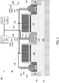
- FIG. 2 is a cross-sectional view illustrating an ESD protection device according to another embodiment of the present invention.
- an ESD protection device 20 includes structures similar to the ESD protection device 10 shown in FIG. 1 .
- a gate structure 230 shown in FIG. 2 includes a gate insulating layer 231 and spacers 233, similar to the gate insulating layer 131 and spacers 133, respectively, as shown in FIG. 1 .
- Gate structure 230 further includes a gate electrode 232. These and other similar components are not described here.
- gate 232 may include: a work function adjustment layer 2322 on the gate insulating layer 231 and a conductive material layer 2321 on the work function adjustment layer 2322.
- the material of the conductive material layer 2321 may include a metal such as tungsten, for example.
- the P-type work function adjustment layer 2322 can raise the gate threshold voltage of the VT as compared with the gate threshold voltage of the N-type work function adjustment layer.
- the gate threshold voltage VT can be raised from the original raised to 0.1V ⁇ 0.4V to 0.6V ⁇ 1.2V, so that it will be more difficult for the channel to form. Therefore, when the ESD protection device is turned on, the current flowing through the fin 120 through a large area, not forming a large local current. It is also easier to dissipate the heat from the current flow.
- the ESD protection device can reduce the possibility of ESD performance degradation, and also protect the internal circuit.
Landscapes
- Semiconductor Integrated Circuits (AREA)
- Metal-Oxide And Bipolar Metal-Oxide Semiconductor Integrated Circuits (AREA)
- Chemical & Material Sciences (AREA)
- Engineering & Computer Science (AREA)
- Composite Materials (AREA)
- Materials Engineering (AREA)
Abstract
Description
- This application claims priority to Chinese patent application No.
201610626293.3, filed on August 2, 2016 - Embodiments of the present invention relates to semiconductor technology, and particularly relates to an electrostatic discharge (ESD) protection device and method.
- As MOSFET (Metal Oxide Semiconductor Field Effect Transistor) device size is gradually reduced, the short channel effect becomes a key issue. FINFET (Fin Field Effect Transistor) devices exhibit good channel charge control, which can further reduce the size of CMOS devices.
- With continued scaling, the devices are more susceptible to Electrostatic discharge (ESD) damage. Electrostatic discharge (ESD) is the sudden flow of electricity between two electrically charged objects caused by contact, an electrical short, or dielectric breakdown. ESD can cause damage to sensitive electronic devices. Conventional ESD protection circuits based on MOSFET device can be adapted to FINFET device.
- However, the inventor has identified drawbacks of using FINFET devices in ESD protection circuits. For example, fin-type gate controlled devices are relatively narrow. When FINFET devices are used as the ESD protection devices, they are prone to relatively poor heat dissipation, leading to serious problems of self-heating, which may result in ESD device performance degradation.
- It is an object of the present invention to provide an improved FINFET-based ESD protection device and method.
- The object is achieved by the features of the respective independent claims. Further embodiments are defined in the respective dependent claims.
- According to a first aspect of the present invention, an electrostatic discharge (ESD) protection device includes a semiconductor substrate and a semiconductor fin located on the semiconductor substrate. The semiconductor fin includes a well region, a first doped region, and a second doped region. The first doped region and the second doped region are respectively adjacent to and being separated by a first portion of the well region. The device also includes a first gate structure on the semiconductor fin between the first doped region and the second doped region, and a first conductive structure electrically connecting the gate structure and the first doped region to a same potential.
- Preferably, the well region has a first conductivity type, the first doped region has the first conductivity type with a dopant concentration greater than the dopant concentration of the well region. Preferably, the second doped region has a second conductivity type opposite to the first conductivity type and has a dopant concentration greater than the dopant concentration of the well region.
- Preferably, the first conductivity type is P-type and the second conductivity type is N-type. In this case, the first conductive structure electrically connects the gate structure and the first doped region to a ground terminal, and the second doped region electrically connects to a signal input terminal for receiving an external signal which includes a positive pulse voltage signal. When the positive pulse voltage signal is greater than a first predetermined threshold, the ESD protection device is turned on, and a current flows from the second doped region into the first doped region.
- Preferably, the first conductivity type is N-type and the second conductivity type is P-type. In this case, the first conductive structure electrically connects the gate structure and the first doped region to a voltage supply terminal, the second doped region electrically connects the second doped region to a signal input terminal for receiving an external signal which includes a negative pulse voltage signal. When the negative pulse voltage signal is less than a first predetermined threshold, the ESD protection device is turned on, and a current flows from the second doped region into the first doped region and third doped region.
- Preferably, the ESD device also includes a third doped region, separated from the second doped region by a second portion of the well region, and a second gate structure on the semiconductor fin and disposed between the second doped region and the third doped region. The ESD device also has a second conductive structure electrically connecting the second gate structure and the third doped region to the same potential as the first gate structure and the first doped region.
- Preferably, the well region has a first conductivity type. The first doped region and the third doped region have the first conductivity type with a dopant concentration greater than the dopant concentration of the well region. The second doped region has a second conductivity type opposite to the first conductivity type and has a dopant concentration greater than the dopant concentration of the well region.
- The first conductivity type may be P-type, then the second conductivity type is N-type. In this case, the first conductive structure and the second conductive structure electrically connect the first gate structure, the second gate structure, the first doped region, and the third doped region to a ground terminal. The second doped region is electrically connected to a signal input terminal for receiving an external signal which includes a positive pulse voltage signal. When the positive pulse voltage signal is greater than a first predetermined threshold, the ESD protection device is turned on, and a current flows from the second doped region into the first doped region and third doped region.
- Alternatively, the first conductivity type may be N-type, then the second conductivity type is P-type. The first conductive structure and the second conductive structure electrically connects the first gate structure, the second gate structure, the first doped region, and the third doped region to a voltage supply terminal. The second doped region electrically connects to a signal input terminal for receiving an external signal which includes a negative pulse voltage signal. When the negative pulse voltage signal is less than a first predetermined threshold, the ESD protection device is turned on, and a current flows from the second doped region into the first doped region and third doped region.
- Preferably, the first gate includes a gate insulator layer, a work function adjustment layer on the gate insulator layer, and a layer of conductive material on the work function adjustment layer.
- Here, the first conductivity type may be P-type, then the second conductivity type is N-type, and the work function adjustment layer is a P-type work function adjustment layer. Preferably, the P-type work function adjustment layer comprises titanium nitride or tantalum nitride.
- Alternatively, the first conductivity type is N-type, then the second conductivity type is P-type, and the work function adjustment layer is an N-type work function adjustment layer. Preferably, the material of N-type work function adjustment layer comprises a titanium alloy.
- According to a second aspect of the present invention, a method for providing ESD (Electrostatic Discharge) protection for a circuit includes providing an ESD protection device, which includes forming a semiconductor substrate and forming a semiconductor fin located on the semiconductor substrate. The semiconductor fin includes a well region, a first doped region, and a second doped region. The first doped region and the second doped region are respectively adjacent to and separated by a first portion of the well region. Providing the ESD protection device also includes forming a first gate structure on the semiconductor fin. The method includes electrically connecting the first gate structure and the first doped region to a same potential, and electrically connecting the second doped region to a signal input terminal for receiving an external signal. The ESD protection device is disposed at a position between the external signal and a circuit configured for receiving the external signal.
- Preferably, the well region has a first conductivity type. The first doped region has the first conductivity type with a dopant concentration greater than the dopant concentration of the well region. The second doped region has a second conductivity type opposite to the first conductivity type and has a dopant concentration greater than the dopant concentration of the well region.
- The first conductivity type may be P-type, then the second conductivity type is N-type. In this case, the first conductive structure electrically connects the first gate structure and the first doped region to a ground terminal. The second doped region is electrically connected to a signal input terminal for receiving an external signal which includes a positive pulse voltage signal. When the positive pulse voltage signal is greater than a first predetermined threshold, the ESD protection device is turned on, and a current flows from the second doped region into the first doped region.
- Alternatively, the first conductivity type is N-type, then the second conductivity type is P-type. In this case, the first conductive structure electrically connects the first gate structure and the first doped region to a voltage supply terminal. The second doped region electrically connects the second doped region to a signal input terminal for receiving an external signal which includes a negative pulse voltage signal. When the negative pulse voltage signal is less than a first predetermined threshold, the ESD protection device is turned on, and a current flows from the second doped region into the first doped region and third doped region.
- Preferably, providing an ESD protection device also includes forming a third doped region, separated from the second doped region by a second portion of the well region, and forming a second gate structure on the semiconductor fin and disposed between the second doped region and the third doped region. The method also includes electrically connecting the second gate structure and the third doped region to the same potential as the first gate structure and the first doped region.
- Preferably, the well region has a first conductivity type, the first doped region and the third doped region have the first conductivity type with a dopant concentration greater than the dopant concentration of the well region, and the second doped region has a second conductivity type opposite to the first conductivity type and has a dopant concentration greater than the dopant concentration of the well region.
- The first conductivity type may be P-type, then the second conductivity type is N-type. In this case, the method includes electrically connecting the firs gate structure, the second gate structure, the first doped region, and the third doped region to a ground terminal. The method also includes electrically connecting the second doped region to a signal input terminal for receiving an external signal which includes a positive pulse voltage signal. When the positive pulse voltage signal is greater than a first predetermined threshold, the ESD protection device is turned on, and current flows from the second doped region into the first doped region and third doped region.
- Alternatively, the first conductivity type is N-type, then the second conductivity type is P-type. In this case, the method includes electrically connecting the first gate structure, the second gate structure, the first doped region, and the third doped region to a voltage supply terminal. The method also includes electrically connecting the second doped region to a signal input terminal for receiving an external signal which includes a negative pulse voltage signal. When the negative pulse voltage signal is less than a first predetermined threshold, the ESD protection device is turned on, and current flows from the second doped region into the first doped region and third doped region.
- Preferably, the electrical connection of the gate structure is enabled to the same potential with the first doped region.
- Preferably, in use of the gate structure, the first doped region is electrically connected to the same potential, so that the ESD protection device does not form a channel during operation, such that when the current flows through the ESD protection device, the current can flow over the larger area of the fin, and does not form a large local current in a channel region. Thereby, device heating can be reduced, reducing the likelihood of degradation of the performance of the ESD protection device.
- Further, if required, the channel may be made more difficult to turn on by incorporating a suitable working function adjustment layer in the gate structure.
- The device according to the first aspect of the present invention may be obtained by a method according to the second aspect of the present invention.
- Other features and advantages of the present invention will become apparent from the following detailed description of exemplary embodiments of the invention with reference to the accompanying drawings.
-
-
FIG 1 is a cross-sectional view illustrating an ESD protection device according to some embodiments of the present invention; -
FIG. 2 is a cross-sectional view illustrating an ESD protection device according to another embodiment of the present invention; -
FIG. 3 is a cross-sectional view illustrating an ESD protection device according to yet another embodiment of the present invention; and -
FIG. 4 is a flowchart illustrating a method for protecting circuit against ESD according to an embodiment of the present invention. - Various exemplary embodiments of the present invention will now be described in detail with reference to the accompanying drawings. It should be noted that the relative arrangement, numerical expression and numerical values of the components and steps set forth in these embodiments, unless otherwise specified, do not limit the invention. At the same time, it will be appreciated that the dimensions of the various portions shown in the drawings are not drawn to scale in actuality for ease of description.
- The following description of at least one exemplary embodiment is merely illustrative and is in no way intended as a limitation on the invention, its application or use. The techniques, methods, and apparatus known to those of ordinary skill in the relevant art may not be discussed in detail, but the techniques, methods, and apparatuses, as appropriate, should be considered as part of the specification. In all examples shown and discussed herein, any specific value should be construed as merely exemplary and not as limiting. Thus, other examples of exemplary embodiments may have different values. It should be noted that like reference numerals and letters designate like items in the following drawings, and therefore, once an item is defined in a drawing, it is not necessary to further discuss it in the subsequent figures.
-
FIG. 1 is a cross-sectional view illustrating an ESD protection device according to some embodiments of the present invention. As shown inFIG. 1 , theESD protection device 10 may include a semiconductor substrate (e.g. silicon substrate) 110, a semiconductor fin (e.g. silicon fin) 120 overlying thesemiconductor substrate 120, and agate structure 130overlying semiconductor fin 120. The semiconductor fin can comprise: a well region (also referred to as a first region) 125, a firstdoped region 121, and a seconddoped region 122. The firstdoped region 121 and the seconddoped regions 122 are adjacent to and being spaced apart from each other by aportion 126 of thewell region 125. Thegate structure 130 is electrically connected, via aconductive structure 155, which can be an interconnect line, to the same potential as thefirst doping region 121. - In one embodiment, the
well region 125 has a first conductivity type. The firstdoped region 121 has the first conductivity type, whose doping concentration greater than a doping concentration of thewell region 125. The seconddoped region 122 has a second conductivity type opposite the first conductivity type, whose doping concentration is greater than the doping concentration of thewell region 125. The gate structure and the first doped region are electrically connected to the same potential, so that the ESD protection device does not turn on the channel during operation, allowing the current through the ESD protection device to flow through a larger region in the fin. This device can prevent large localized current and can reduce device heating, thereby reducing the likelihood of degradation of the ESD protection device performance. - In one embodiment,
gate structure 130 may include agate insulator layer 131 on the surface portion of the semiconductor fins 120 (which may comprise, for example, a silicon oxide layer), agate electrode 132 on thegate insulator layer 131, and spacer regions 133 (e.g. silicon oxide and/or silicon nitride) on both side surfaces of thegate electrode 132. Thegate electrode 132 is electrically connected to the firstdoped region 121 to the same potential. The seconddoped region 122 is electrically connected to a signal input terminal (not shown) receiving anexternal signal 170. - As shown in
FIG. 1 ,ESD protection device 10 may further include afirst electrode 141 in the firstdoped region 121 and asecond electrode 142 in the seconddoped region 122. - In one embodiment, shown in
FIG. 1 , theESD protection device 10 may further include afirst contact member 151 in contact with thefirst electrode 141, and asecond contact member 152 in contact with thesecond electrode 142. Thefirst contact member 151 is connected to thegate electrode 132 throughconductive structure 155, and thesecond contact member 152 is electrically connected through anotherconductive structure 157 to a signal input terminal (not shown) for receiving an external signal. In other words,gate 132 is connected to thefirst electrode 141 and thefirst doping region 121 through thefirst contact member 151. Thesecond doping region 122 is connected to a signal input for receiving an external signal through thesecond electrode 142 and thesecond contact member 152.Conductive structure 157 is provided for connecting the seconddoped region 122 to anexternal signal 170 at a point between theexternal signal 170 and acircuit 180 to be protected. - In one embodiment, shown in
FIG. 1 , thesemiconductor substrate 110 may include asecond region 111 having a first conductivity type. Thesecond region 111 is adjacent to thewell region 125. For example, the doping concentration of thesecond region 111 can have a doping concentration the same as that in thewell region 125. Thesecond region 111 and thewell region 125 may be used together as a well region. - In a particular application, the
gate electrode 132 is electrically connected to the firstdoped region 121 to the same potential. The seconddoped region 122 is electrically connected to the signal input terminal (not shown) for receiving an external signal. Here, the external signal can enter through the signal input terminal to the protected internal circuit. That is, the ESD protection device may be disposed at a position where the external signal enters the internal circuit. The following examples illustrate various embodiments in conjunction with the ESD protection device during operation. - In one embodiment, the first conductivity type is P-type and the second conductivity type is N-type. The
gate electrode 132 is electrically connected to the firstdoped region 121 to the ground. The external signal may be a positive pulse voltage signal. In this embodiment, the conductivity type of thewell region 125 may be, for example, P-type. The conductivity type first dopedregion 121 may be, for example, P + type (here, "P + type" indicates that the conductivity type is P-type and the doping concentration is greater than the P-type doping concentration of the well region.). The conductivity type of the seconddoped region 122 may be, for example, N + type (here, "N +" represents an N-type conductivity type and the doping concentration is greater than the N-type doping of the well region.) In this case, thegate 132 is electrically connected to the firstdoped region 121 to the ground terminal, the seconddoped region 122 is electrically connected to the signal input terminal receiving an external signal, where the external signal is a positive pulse voltage signal. When the voltage of the external positive pulse signal is greater than a first predetermined threshold value (e.g. the first predetermined threshold value may be a positive value), i.e. when the seconddoped region 122 has excessive positive charge, the ESD protection device is turned on, generating a current from the seconddoped region 122 to the firstdoped region 121. Since thegate 132 is connected to ground, no channel is formed in thewell region 125, thus generating a current flowing through thefin 120 over a large area, not forming a large local current. It is also easier to dissipate the heat from the current flow. The ESD protection device can reduce the possibility of ESD performance degradation, and also protect the internal circuit. - In another embodiment, the first conductivity type is N-type and the second conductivity type is P-type.
Gate electrode 132 is electrically connected to the firstdoped region 121 to a supply voltage terminal (VDD). The external signal may be a negative pulse voltage signal. In this embodiment, the conductivity type of thewell region 125 may be, for example, N-type, the conductivity type of the firstdoped region 121 may be, for example, N + type, the conductivity type of the seconddoped region 122 may be, for example, P + type. In this case, thegate 132 is electrically connected to the firstdoped region 121 to the supply voltage terminal. The seconddoped region 122 is electrically connected to the signal input terminal for receiving an external signal, where the external signal is a negative pulse voltage signal. When a negative pulse voltage signal is less than a second preset threshold (e.g., the second predetermined threshold value can be negative), i.e., with thesecond doping region 122 having excessive negative charges, the ESD protection device is turned on, generating a current from the firstdoped region 121 to the seconddoped region 122. Since thegate 132 is connected to a supply voltage terminal, no channel can be formed in thewell region 125. Therefore, the current flowing through thefin 120 through a large area, not forming a large local current. It is also easier to dissipate the heat from the current flow. The ESD protection device can reduce the possibility of ESD performance degradation, and also protect the internal circuit. -
FIG. 2 is a cross-sectional view illustrating an ESD protection device according to another embodiment of the present invention. As shown, anESD protection device 20 includes structures similar to theESD protection device 10 shown inFIG. 1 . For example, agate structure 230 shown inFIG. 2 includes agate insulating layer 231 andspacers 233, similar to thegate insulating layer 131 andspacers 133, respectively, as shown inFIG. 1 .Gate structure 230 further includes agate electrode 232. These and other similar components are not described here. - In one embodiment, as shown in
FIG. 2 ,gate 232 may include: a workfunction adjustment layer 2322 on thegate insulating layer 231 and aconductive material layer 2321 on the workfunction adjustment layer 2322. The material of theconductive material layer 2321 may include a metal such as tungsten, for example. - In one embodiment, the first conductivity type is P-type, the second conductivity type is N-type, and the work
function adjustment layer 2322 is a P-type work function adjustment layer. For example, the material of the P-type work function adjustment layer may include titanium nitride (TiN) or tantalum nitride (TaN). In this embodiment, the conductivity type of thewell region 125 may be, for example, P-type, the conductivity type of the firstdoped region 121 may be, for example, P + type, and the conductivity type of the seconddoped region 122 may be, for example, N + type. In this case, the P-type workfunction adjustment layer 2322 can raise the gate threshold voltage of the VT as compared with the gate threshold voltage of the N-type work function adjustment layer. For example, the gate threshold voltage VT can be raised from the original raised to 0.1V ∼ 0.4V to 0.6V ∼ 1.2V, so that it will be more difficult for the channel to form. Therefore, when the ESD protection device is turned on, the current flowing through thefin 120 through a large area, not forming a large local current. It is also easier to dissipate the heat from the current flow. The ESD protection device can reduce the possibility of ESD performance degradation, and also protect the internal circuit. - In another embodiment, the first conductivity type is N-type, the second conductivity type is P-type, and the work
function adjustment layer 2322 is an N-type work function adjustment layer. For example, the material of the N-type work function adjustment layer may include titanium aluminum alloy (TiAl). In this embodiment, the conductivity type of thewell region 125 may be, for example, N-type, the conductivity type of the firstdoped region 121 may be, for example, N + type, and the conductivity type of the seconddoped region 122 may be, for example, P + type. In this case, the N-type workfunction adjustment layer 2322 can raise the gate threshold voltage of the VT as compared with the gate threshold voltage of the P-type work function adjustment layer. For example, the gate threshold voltage VT can be raised from the original raised to 0.1V ∼ 0.4V to 0.6V ∼ 1.2V, so that it will be more difficult for the channel to form. Therefore, when the ESD protection device is turned on, the current flowing through thefin 120 through a large area, not forming a large local current. It is also easier to dissipate the heat from the current flow. The ESD protection device can reduce the possibility of ESD performance degradation, and also protect the internal circuit. -
FIG. 3 is a cross-sectional view illustrating an ESD protection device according to another embodiment of the present invention. As shown inFIG. 3 , anESD protection device 30 includes components similar to those ofESD protection devices FIG. 1 andFIG. 2 , respectively. Therefore, those components are not described in detail. - In one embodiment, as shown in
FIG. 3 , thesemiconductor fin 120 includes a firstdoped region 121, a seconddoped region 122, and athird region 123 spaced from the seconddoped region 122. The thirddoped region 123 has dopants with a first conductivity type. In an embodiment, the doping concentration of thethird doping region 123 is greater than the doping concentration of thewell region 125, which forms a well region in the device. It can be seen inFIG. 3 that the firstdoped region 121 and the seconddoped region 122 are adjacent to and are separated by afirst portion 126 ofwell region 125. The seconddoped region 122 and the thirddoped region 123 are adjacent to and are separated by asecond portion 127 ofwell region 125. - In one embodiment, shown in
FIG. 3 , the gate structure may include afirst gate structure 330 over thesemiconductor fin 120 and between the firstdoped region 121 and the seconddoped region 122. The gate structure may also include asecond gate structure 430 over thesemiconductor fin 120 and between the seconddoped region 122 and the thirddoped region 123. Here, thefirst gate structure 330 and thesecond gate structure 430 are similar to thegate structure 230 ofFIG. 2 . For example, thefirst gate structure 330 includes a firstgate insulating layer 331, a gate electrode 332 (which includes a work function adjustment layer 3322 and a conductive material layer 3321), andspacers 333, which are similar to thegate structure 230 ofFIG. 2 , which includesgate insulating layer 231, gate electrode 232 (which includes workfunction adjustment layer 2322 and conductive material layer 2321) andspacers 233. As another example, thesecond gate structure 430 includes agate insulating layer 431, a gate electrode 332 (which includes a workfunction adjustment layer 4322 and a conductive material layer 4321), andspacers 433, which are similar to thegate structure 230 ofFIG. 2 , which includesgate insulating layer 231, gate electrode 232 (which includes workfunction adjustment layer 2322 and conductive material layer 2321) andspacers 233. - In one embodiment, as shown in
FIG. 3 , gate electrode 332 of thefirst gate structure 330,gate electrode 432 of the second gate structure of the 430, the firstdoped region 121, and the thirddoped region 123 are electrically connected to the same potential. A firstconductive structure 155 and a secondconductive structure 156 are used for these connections.Conductive structures Conductive structure 157 is provided for connecting the seconddoped region 122 to anexternal signal 170 at a point between theexternal signal 170 and acircuit 180 to be protected. - In one embodiment, as shown in
FIG. 3 , theESD protection device 30 may further include athird electrode 143 partially formed in the thirddoped region 123 insemiconductor fin 120. Athird contact member 153 is connected to thethird electrode 143. Thethird contact member 153 is also connected togate electrode 432 of the second gate structure 40. - The following examples illustrate various embodiments in conjunction with the operation of the
ESD protection device 30. - In one embodiment, the first conductivity type is P-type and the second conductivity type is N-type. Gate electrode 332 of the first gate structure of the 330,
gate electrode 432 of thesecond gate structure 430, the firstdoped region 121, and the thirddoped region 123 are electrically connected to a ground terminal. The external signal may be a positive pulse voltage signal. In this embodiment, the conductivity type of thewell region 125 may be, for example, P-type. the conductivity type of thefirst doping region 121 and thethird doping region 123 are P + type, for example. The seconddoped region 122 may be N + type. In this case, Gate electrode 332 of the first gate structure of the 330,gate electrode 432 of thesecond gate structure 430, the firstdoped region 121, and the thirddoped region 123 are electrically connected to a ground terminal. The seconddoped region 122 is electrically connected to the signal input terminal (not shown) for receiving an external signal, which is a positive pulse voltage signal. When the voltage of the external positive pulse signal is greater than a first predetermined threshold value, i.e., the seconddoped region 122 has excess positive charges accumulated, the ESD protection device is turned on. Under this condition, a current flows from the seconddoped region 122 to the firstdoped region 121 and the thirddoped region 123. Since thegate structures 332 and 432 are connected to the ground terminal, a conductive channel cannot be formed in thewell region 125. Therefore, the current flows through thefin 120 over a large area, and not form a large localized current. The absence of a channel can reduce localized heating. ESDprotective device 30 as shownFIG. 3 has a structure includes three doped regions enables the current to disperse in a large area of the fin structure. The ESD protection device can protect the internal circuit, and the likelihood of the ESD protection device performance degradation is reduced. - In another embodiment, the first conductivity type is N-type and the second conductivity type is P-type. Gate electrode 332 of the first gate structure of the 330,
gate electrode 432 of thesecond gate structure 430, the firstdoped region 121, and the thirddoped region 123 are electrically connected to a voltage supply terminal (not shown). The external signal may be a negative pulse voltage signal. In this embodiment, the conductivity type of thewell region 125 may be, for example, N-type. the conductivity type of thefirst doping region 121 and thethird doping region 123 are N + type, for example. The seconddoped region 122 may be P + type. In this case, Gate electrode 332 of the first gate structure of the 330,gate electrode 432 of thesecond gate structure 430, the firstdoped region 121, and the thirddoped region 123 are electrically connected to a voltage supply terminal. The seconddoped region 122 is electrically connected to the signal input terminal (not shown) for receiving an external signal, which is a negative pulse voltage signal. When the voltage of the external negative pulse signal is greater than a second predetermined threshold value, i.e., the seconddoped region 122 has excess negative charges accumulated, the ESD protection device is turned on. Under this condition, a current flows from the firstdoped region 121 and the thirddoped region 123 to the seconddoped region 122. Since thegate structures 332 and 432 are connected to the voltage supply terminal, a conductive channel cannot be formed in thewell region 125. Therefore, the current flows through thefin 120 over a large area, and not form a large localized current. The absence of a channel can reduce localized heating. ESDprotective device 30 as shownFIG. 3 has a structure includes three doped regions enables the current to disperse in a large area of the fin structure. The ESD protection device can protect the internal circuit, and the likelihood of the ESD protection device performance degradation is reduced. -
FIG. 4 is aflowchart 400 illustrating a method for protecting circuit against ESD according to an embodiment of the present invention. The method described below can be further illustrated withFIGS. 1-3 and the accompanying text. - According to some embodiments of the present invention, a method for providing ESD (Electrostatic Discharge) protection for a circuit includes providing an ESD protection device (410), which includes forming a semiconductor substrate (420) and forming a semiconductor fin located on the semiconductor substrate (430). The semiconductor fin includes a well region, a first doped region, and a second doped region. The first doped region and the second doped region are respectively adjacent to and separated by a first portion of the well region. Providing the ESD protection device also includes forming a first gate structure on the semiconductor fin (440). The method includes electrically connecting the first gate structure and the first doped region to a same potential (450), and electrically connecting the second doped region to a signal input terminal for receiving an external signal (460). The method also includes connecting the external signal to the circuit to be protected (470).
- In an embodiment of the above method, the well region has a first conductivity type. The first doped region has the first conductivity type with a dopant concentration greater than the dopant concentration of the well region. The second doped region has a second conductivity type opposite to the first conductivity type and has a dopant concentration greater than the dopant concentration of the well region.
- In an embodiment, the first conductivity type is P-type and the second conductivity type is N-type. In this case, the first conductive structure electrically connects the first gate structure and the first doped region to a ground terminal. The second doped region is electrically connected to a signal input terminal for receiving an external signal which includes a positive pulse voltage signal. When the positive pulse voltage signal is greater than a first predetermined threshold, the ESD protection device is turned on, and a current flows from the second doped region into the first doped region.
- In an embodiment, the first conductivity type is N-type and the second conductivity type is P-type. In this case, the first conductive structure electrically connects the first gate structure and the first doped region to a voltage supply terminal. The second doped region electrically connects the second doped region to a signal input terminal for receiving an external signal which includes a negative pulse voltage signal. When the negative pulse voltage signal is less than a first predetermined threshold, the ESD protection device is turned on, and a current flows from the second doped region into the first doped region and third doped region.
- In an embodiment, providing an ESD protection device also includes (430) forming a third doped region, separated from the second doped region by a second portion of the well region, and forming a second gate structure (440) on the semiconductor fin and disposed between the second doped region and the third doped region. The method also includes electrically connecting the second gate structure and the third doped region to the same potential as the first gate structure and the first doped region.
- In an embodiment, the well region has a first conductivity type, the first doped region and the third doped region have the first conductivity type with a dopant concentration greater than the dopant concentration of the well region, and the second doped region has a second conductivity type opposite to the first conductivity type and has a dopant concentration greater than the dopant concentration of the well region.
- In an embodiment, the first conductivity type is P-type and the second conductivity type is N-type. In this case, the method includes electrically connecting the first gate structure, the second gate structure, the first doped region, and the third doped region to a ground terminal. The method also includes electrically connecting the second doped region to a signal input terminal for receiving an external signal which includes a positive pulse voltage signal. When the positive pulse voltage signal is greater than a first predetermined threshold, the ESD protection device is turned on, and current flows from the second doped region into the first doped region and third doped region.
- In an embodiment, the first conductivity type is N-type and the second conductivity type is P-type. In this case, the method includes electrically connecting the first gate structure, the second gate structure, the first doped region, and the third doped region to a voltage supply terminal. The method also includes electrically connecting the second doped region to a signal input terminal for receiving an external signal which includes a negative pulse voltage signal. When the negative pulse voltage signal is less than a first predetermined threshold, the ESD protection device is turned on, and current flows from the second doped region into the first doped region and third doped region.
Claims (15)
- An electrostatic discharge, ESD, protection device, comprising:a semiconductor substrate;a semiconductor fin located on the semiconductor substrate, the semiconductor fin comprising:a well region;a first doped region; anda second doped region, wherein the first doped region and the second doped region are respectively adjacent to and being separated by a first portion of the well region;a first gate structure on said semiconductor fin between the first doped region and the second doped region;a first conductive structure electrically connecting the gate structure and the first doped region to a same potential; anda second conductive structure for connecting the second doped region to a point between an external signal and a circuit to be protected.
- The device of claim 1, wherein:the well region has a first conductivity type;the first doped region has the first conductivity type with a dopant concentration greater than the dopant concentration of the well region; andthe second doped region has a second conductivity type opposite to the first conductivity type and has a dopant concentration greater than the dopant concentration of the well region.
- The device of claim 2, wherein
the first conductivity type is P-type and the second conductivity type is N-type, and wherein: the first conductive structure electrically connects the gate structure and the first doped region to a ground terminal; the second doped region electrically connects to a signal input terminal for receiving an external signal which includes a positive pulse voltage signal; wherein, when the positive pulse voltage signal is greater than a first predetermined threshold, the ESD protection device is turned on, and a current flows from the second doped region into the first doped region; or, alternatively,
the first conductivity type is N-type and the second conductivity type is P-type, and wherein: the first conductive structure electrically connects the gate structure and the first doped region to a voltage supply terminal; the second doped region electrically connects the second doped region to a signal input terminal for receiving an external signal which includes a negative pulse voltage signal; wherein, when the negative pulse voltage signal is less than a first predetermined threshold, the ESD protection device is turned on, and a current flows from the second doped region into the first doped region and third doped region. - The device of claim 1, further comprising:a third doped region, separated from the second doped region by a second portion of the well region;a second gate structure on the semiconductor fin and disposed between the second doped region and the third doped region; anda third conductive structure electrically connecting the second gate structure and the third doped region to the same potential as the first gate structure and the first doped region.
- The device of claim 4, wherein:the well region has a first conductivity type;the first doped region and the third doped region have the first conductivity type with a dopant concentration greater than the dopant concentration of the well region; andthe second doped region has a second conductivity type opposite to the first conductivity type and has a dopant concentration greater than the dopant concentration of the well region.
- The device of claim 5, wherein
the first conductivity type is P-type and the second conductivity type is N-type, and wherein: the first conductive structure and the third conductive structure electrically connect the first gate structure, the second gate structure, the first doped region, and the third doped region to a ground terminal; the second doped region electrically connects to a signal input terminal for receiving an external signal which includes a positive pulse voltage signal; wherein, when the positive pulse voltage signal is greater than a first predetermined threshold, the ESD protection device is turned on, and a current flows from the second doped region into the first doped region and third doped region; or, alternatively,
the first conductivity type is N-type and the second conductivity type is P-type, and wherein: the first conductive structure and the third conductive structure electrically connects the first gate structure, the second gate structure, the first doped region, and the third doped region to a voltage supply terminal; the second doped region electrically connects to a signal input terminal for receiving an external signal which includes a negative pulse voltage signal; wherein, when the negative pulse voltage signal is less than a first predetermined threshold, the ESD protection device is turned on, and a current flows from the second doped region into the first doped region and third doped region. - The device of anyone of the claims 1-6, wherein the first gate structure comprises:a gate insulator layer;a work function adjustment layer on the gate insulator layer; anda layer of conductive material on the work function adjustment layer.
- The device of claim 7, wherein
the first conductivity type is P-type and the second conductivity type is N-type, and the work function adjustment layer is a P-type work function adjustment layer, the P-type work function adjustment layer including titanium nitride or tantalum nitride; or, alternatively,
the first conductivity type is N-type and the second conductivity type is P-type, and the work function adjustment layer is an N-type work function adjustment layer, wherein the material of N-type work function adjustment layer comprises a titanium alloy. - A method for providing Electrostatic Discharge, ESD, protection for a circuit, characterized by comprising:forming an ESD protection device, comprising:providing a semiconductor substrate;forming a semiconductor fin located on the semiconductor substrate, said semiconductor fin including a well region, a first doped region, and a second doped region, wherein the first doped region and the second doped region are respectively adjacent to and separated by a first portion of the well region; andforming a first gate structure on the semiconductor fin;electrically connecting the first gate structure and the first doped region to a same potential;electrically connecting the second doped region to a signal input terminal for receiving an external signal; andconnecting the external signal and a circuit to be protected.
- The method of claim 9, wherein:the well region has a first conductivity type;the first doped region has the first conductivity type with a dopant concentration greater than the dopant concentration of the well region; andthe second doped region has a second conductivity type opposite to the first conductivity type and has a dopant concentration greater than the dopant concentration of the well region.
- The method of claim 10, wherein
the first conductivity type is P-type and the second conductivity type is N-type, and wherein: the first conductive structure electrically connects the first gate structure and the first doped region to a ground terminal; the second doped region electrically connects to a signal input terminal for receiving an external signal which includes a positive pulse voltage signal; wherein, when the positive pulse voltage signal is greater than a first predetermined threshold, the ESD protection device is turned on, and a current flows from the second doped region into the first doped region; or, alternatively,
the first conductivity type is N-type and the second conductivity type is P-type, and wherein: the first conductive structure electrically connects the first gate structure and the first doped region to a voltage supply terminal; the second doped region electrically connects the second doped region to a signal input terminal for receiving an external signal which includes a negative pulse voltage signal; wherein, when the negative pulse voltage signal is less than a first predetermined threshold, the ESD protection device is turned on, and a current flows from the second doped region into the first doped region and third doped region. - The method of claim 9, wherein providing an ESD protection device further comprises:forming a third doped region in the fin, separated from the second doped region by a second portion of the well region; andforming a second gate structure on the semiconductor fin and disposed between the second doped region and the third doped region;wherein the method further comprises electrically connecting the second gate structure and the third doped region to the same potential as the first gate structure and the first doped region.
- The method of claim 12, wherein,
the well region has a first conductivity type;
the first doped region and the third doped region have the first conductivity type with a dopant concentration greater than the dopant concentration of the well region; and
the second doped region has a second conductivity type opposite to the first conductivity type and has a dopant concentration greater than the dopant concentration of the well region. - The method of claim 13, wherein
the first conductivity type is P-type and the second conductivity type is N-type, and wherein the method comprises: electrically connecting the first gate structure, the second gate structure, the first doped region, and the third doped region to a ground terminal; electrically connecting the second doped region to a signal input terminal for receiving an external signal which includes a positive pulse voltage signal; wherein, when the positive pulse voltage signal is greater than a first predetermined threshold, the ESD protection device is turned on, and current flows from the second doped region into the first doped region and third doped region; or, alternatively,
the first conductivity type is N-type and the second conductivity type is P-type, and wherein the method comprises: electrically connecting the gate structure, the first doped region, and the third doped region to a voltage supply terminal; electrically connecting the second doped region to a signal input terminal for receiving an external signal which includes a negative pulse voltage signal; wherein, when the negative pulse voltage signal is less than a first predetermined threshold, the ESD protection device is turned on, and current flows from the second doped region into the first doped region and third doped region. - The method of anyone of the claims 9-14, wherein the first gate structure comprises a work function adjustment layer to increase a threshold voltage of the ESD protection device.
Applications Claiming Priority (1)
| Application Number | Priority Date | Filing Date | Title |
|---|---|---|---|
| CN201610626293.3A CN107680956B (en) | 2016-08-02 | 2016-08-02 | Electrostatic discharge ESD protection device and method for protecting circuit |
Publications (1)
| Publication Number | Publication Date |
|---|---|
| EP3288080A1 true EP3288080A1 (en) | 2018-02-28 |
Family
ID=59520754
Family Applications (1)
| Application Number | Title | Priority Date | Filing Date |
|---|---|---|---|
| EP17184173.7A Withdrawn EP3288080A1 (en) | 2016-08-02 | 2017-08-01 | Electrostatic discharge protection device and method |
Country Status (3)
| Country | Link |
|---|---|
| US (1) | US10797044B2 (en) |
| EP (1) | EP3288080A1 (en) |
| CN (1) | CN107680956B (en) |
Families Citing this family (5)
| Publication number | Priority date | Publication date | Assignee | Title |
|---|---|---|---|---|
| US10680087B2 (en) * | 2018-09-05 | 2020-06-09 | Nxp B.V. | Gated diode having fingers with elevated gates |
| US11521967B2 (en) * | 2019-06-28 | 2022-12-06 | Stmicroelectronics International N.V. | Multi-finger devices with reduced parasitic capacitance |
| US11527528B2 (en) * | 2020-04-21 | 2022-12-13 | Globalfoundries Singapore Pte. Ltd. | Electrostatic discharge protection devices and methods of forming electrostatic discharge protection devices |
| US12166031B2 (en) * | 2020-12-22 | 2024-12-10 | Intel Corporation | Substrate-less electrostatic discharge (ESD) integrated circuit structures |
| CN115249701B (en) * | 2021-04-25 | 2025-09-23 | 中芯国际集成电路制造(上海)有限公司 | Electrostatic discharge protection structure and forming method thereof |
Citations (4)
| Publication number | Priority date | Publication date | Assignee | Title |
|---|---|---|---|---|
| WO1996022613A1 (en) * | 1995-01-20 | 1996-07-25 | Peregrine Semiconductor Corporation | Method and structure for providing esd protection for silicon on insulator integrated circuits |
| US20070267700A1 (en) * | 2006-05-18 | 2007-11-22 | Infineon Technologies Ag | Esd protection element |
| US20120176709A1 (en) * | 2011-01-07 | 2012-07-12 | Taiwan Semiconductor Manufacturing Company, Ltd. | Esd protection devices and methods for forming esd protection devices |
| US20140145249A1 (en) * | 2012-11-29 | 2014-05-29 | Taiwan Semiconductor Manufacturing Company, Ltd. | Diode Structure Compatible with FinFET Process |
Family Cites Families (9)
| Publication number | Priority date | Publication date | Assignee | Title |
|---|---|---|---|---|
| US5199976A (en) * | 1991-06-13 | 1993-04-06 | The Gillette Company | Ozone-friendly correction fluid |
| US20050035410A1 (en) * | 2003-08-15 | 2005-02-17 | Yee-Chia Yeo | Semiconductor diode with reduced leakage |
| US8531805B2 (en) * | 2009-03-13 | 2013-09-10 | Qualcomm Incorporated | Gated diode having at least one lightly-doped drain (LDD) implant blocked and circuits and methods employing same |
| US8461651B2 (en) * | 2010-11-04 | 2013-06-11 | Shanghai Institute Of Microsystem And Information Technology, Chinese Academy Of Sciences | ESD protection devices for SOI integrated circuit and manufacturing method thereof |
| US9082702B2 (en) * | 2012-02-27 | 2015-07-14 | Applied Materials, Inc. | Atomic layer deposition methods for metal gate electrodes |
| US8546209B1 (en) * | 2012-06-15 | 2013-10-01 | International Business Machines Corporation | Replacement metal gate processing with reduced interlevel dielectric layer etch rate |
| CN105336690B (en) * | 2014-06-27 | 2018-06-01 | 中芯国际集成电路制造(上海)有限公司 | The production method of semiconductor devices |
| CN105513969B (en) * | 2014-09-26 | 2018-12-21 | 中芯国际集成电路制造(上海)有限公司 | The forming method of transistor |
| KR20170029799A (en) * | 2015-09-08 | 2017-03-16 | 삼성전자주식회사 | Semiconductor device |
-
2016
- 2016-08-02 CN CN201610626293.3A patent/CN107680956B/en active Active
-
2017
- 2017-07-25 US US15/659,525 patent/US10797044B2/en active Active
- 2017-08-01 EP EP17184173.7A patent/EP3288080A1/en not_active Withdrawn
Patent Citations (4)
| Publication number | Priority date | Publication date | Assignee | Title |
|---|---|---|---|---|
| WO1996022613A1 (en) * | 1995-01-20 | 1996-07-25 | Peregrine Semiconductor Corporation | Method and structure for providing esd protection for silicon on insulator integrated circuits |
| US20070267700A1 (en) * | 2006-05-18 | 2007-11-22 | Infineon Technologies Ag | Esd protection element |
| US20120176709A1 (en) * | 2011-01-07 | 2012-07-12 | Taiwan Semiconductor Manufacturing Company, Ltd. | Esd protection devices and methods for forming esd protection devices |
| US20140145249A1 (en) * | 2012-11-29 | 2014-05-29 | Taiwan Semiconductor Manufacturing Company, Ltd. | Diode Structure Compatible with FinFET Process |
Also Published As
| Publication number | Publication date |
|---|---|
| CN107680956A (en) | 2018-02-09 |
| CN107680956B (en) | 2019-12-03 |
| US10797044B2 (en) | 2020-10-06 |
| US20180040605A1 (en) | 2018-02-08 |
Similar Documents
| Publication | Publication Date | Title |
|---|---|---|
| US9899385B2 (en) | Semiconductor integrated circuit and manufacturing method thereof | |
| US10797044B2 (en) | Electrostatic discharge protection device and method | |
| US6710990B2 (en) | Low voltage breakdown element for ESD trigger device | |
| US20130148243A1 (en) | Esd protecting circuit and semiconductor device including the same | |
| US8587074B2 (en) | Device having a gate stack | |
| JP4320038B2 (en) | Semiconductor integrated circuit | |
| EP3252814A1 (en) | Esd protection device and method | |
| CN112151620B (en) | Junction field effect transistor with ESD protection structure | |
| US9379068B2 (en) | ESD protection semiconductor device | |
| CN106783839B (en) | Electronic equipment specifically for protection against overvoltages | |
| US9978741B2 (en) | High voltage ESD device for finfet technology | |
| CN101371416A (en) | Low capacitance transient voltage suppressor | |
| US9196610B1 (en) | Semiconductor structure and electrostatic discharge protection circuit | |
| Tam et al. | Snapback breakdown ESD device based on zener diodes on silicon-on-insulator technology | |
| CN104979340A (en) | Semiconductor structure and electrostatic discharge protection circuit | |
| JP2006165481A (en) | Semiconductor device | |
| CN110797336B (en) | Electrostatic protection circuit, electrostatic protection device and forming method thereof | |
| US10068896B1 (en) | Electrostatic discharge protection device and manufacturing method thereof | |
| US9386642B2 (en) | Semiconductor device | |
| KR20000020618A (en) | Circuit for protecting electrostatic of semiconductor device | |
| JP3187773B2 (en) | Semiconductor device with input protection element | |
| De Conti et al. | Toward Gated-Diode-BIMOS for thin silicon ESD protection in advanced FD-SOI CMOS technologies | |
| CN116454082A (en) | Electrostatic discharge protection device | |
| TW201539709A (en) | Semiconductor structure and electrostatic discharge protection circuit | |
| CN101826716A (en) | Low voltage transient voltage suppresser with potential barrier Zener diode |
Legal Events
| Date | Code | Title | Description |
|---|---|---|---|
| PUAI | Public reference made under article 153(3) epc to a published international application that has entered the european phase |
Free format text: ORIGINAL CODE: 0009012 |
|
| STAA | Information on the status of an ep patent application or granted ep patent |
Free format text: STATUS: THE APPLICATION HAS BEEN PUBLISHED |
|
| AK | Designated contracting states |
Kind code of ref document: A1 Designated state(s): AL AT BE BG CH CY CZ DE DK EE ES FI FR GB GR HR HU IE IS IT LI LT LU LV MC MK MT NL NO PL PT RO RS SE SI SK SM TR |
|
| AX | Request for extension of the european patent |
Extension state: BA ME |
|
| STAA | Information on the status of an ep patent application or granted ep patent |
Free format text: STATUS: REQUEST FOR EXAMINATION WAS MADE |
|
| 17P | Request for examination filed |
Effective date: 20180807 |
|
| RBV | Designated contracting states (corrected) |
Designated state(s): AL AT BE BG CH CY CZ DE DK EE ES FI FR GB GR HR HU IE IS IT LI LT LU LV MC MK MT NL NO PL PT RO RS SE SI SK SM TR |
|
| RAP1 | Party data changed (applicant data changed or rights of an application transferred) |
Owner name: SEMICONDUCTOR MANUFACTURING INTERNATIONAL (SHANGHA Owner name: SEMICONDUCTOR MANUFACTURING INTERNATIONAL (BEIJING |
|
| STAA | Information on the status of an ep patent application or granted ep patent |
Free format text: STATUS: EXAMINATION IS IN PROGRESS |
|
| 17Q | First examination report despatched |
Effective date: 20200324 |
|
| STAA | Information on the status of an ep patent application or granted ep patent |
Free format text: STATUS: THE APPLICATION IS DEEMED TO BE WITHDRAWN |
|
| 18D | Application deemed to be withdrawn |
Effective date: 20200804 |