EP3288076A1 - A semiconductor die package and method of producing the package - Google Patents
A semiconductor die package and method of producing the package Download PDFInfo
- Publication number
- EP3288076A1 EP3288076A1 EP16185640.6A EP16185640A EP3288076A1 EP 3288076 A1 EP3288076 A1 EP 3288076A1 EP 16185640 A EP16185640 A EP 16185640A EP 3288076 A1 EP3288076 A1 EP 3288076A1
- Authority
- EP
- European Patent Office
- Prior art keywords
- contacts
- die
- connecting device
- insert
- lateral connecting
- Prior art date
- Legal status (The legal status is an assumption and is not a legal conclusion. Google has not performed a legal analysis and makes no representation as to the accuracy of the status listed.)
- Granted
Links
Images



Classifications
-
- H—ELECTRICITY
- H10—SEMICONDUCTOR DEVICES; ELECTRIC SOLID-STATE DEVICES NOT OTHERWISE PROVIDED FOR
- H10W—GENERIC PACKAGES, INTERCONNECTIONS, CONNECTORS OR OTHER CONSTRUCTIONAL DETAILS OF DEVICES COVERED BY CLASS H10
- H10W20/00—Interconnections in chips, wafers or substrates
- H10W20/20—Interconnections within wafers or substrates, e.g. through-silicon vias [TSV]
-
- H—ELECTRICITY
- H03—ELECTRONIC CIRCUITRY
- H03K—PULSE TECHNIQUE
- H03K3/00—Circuits for generating electric pulses; Monostable, bistable or multistable circuits
- H03K3/02—Generators characterised by the type of circuit or by the means used for producing pulses
- H03K3/36—Generators characterised by the type of circuit or by the means used for producing pulses by the use, as active elements, of semiconductors, not otherwise provided for
-
- H—ELECTRICITY
- H10—SEMICONDUCTOR DEVICES; ELECTRIC SOLID-STATE DEVICES NOT OTHERWISE PROVIDED FOR
- H10W—GENERIC PACKAGES, INTERCONNECTIONS, CONNECTORS OR OTHER CONSTRUCTIONAL DETAILS OF DEVICES COVERED BY CLASS H10
- H10W70/00—Package substrates; Interposers; Redistribution layers [RDL]
- H10W70/01—Manufacture or treatment
- H10W70/05—Manufacture or treatment of insulating or insulated package substrates, or of interposers, or of redistribution layers
- H10W70/08—Manufacture or treatment of insulating or insulated package substrates, or of interposers, or of redistribution layers by depositing layers on the chip or wafer, e.g. "chip-first" RDLs
- H10W70/09—Manufacture or treatment of insulating or insulated package substrates, or of interposers, or of redistribution layers by depositing layers on the chip or wafer, e.g. "chip-first" RDLs extending onto an encapsulation that laterally surrounds the chip or wafer, e.g. fan-out wafer level package [FOWLP] RDLs
-
- H—ELECTRICITY
- H10—SEMICONDUCTOR DEVICES; ELECTRIC SOLID-STATE DEVICES NOT OTHERWISE PROVIDED FOR
- H10W—GENERIC PACKAGES, INTERCONNECTIONS, CONNECTORS OR OTHER CONSTRUCTIONAL DETAILS OF DEVICES COVERED BY CLASS H10
- H10W70/00—Package substrates; Interposers; Redistribution layers [RDL]
- H10W70/60—Insulating or insulated package substrates; Interposers; Redistribution layers
-
- H—ELECTRICITY
- H10—SEMICONDUCTOR DEVICES; ELECTRIC SOLID-STATE DEVICES NOT OTHERWISE PROVIDED FOR
- H10W—GENERIC PACKAGES, INTERCONNECTIONS, CONNECTORS OR OTHER CONSTRUCTIONAL DETAILS OF DEVICES COVERED BY CLASS H10
- H10W70/00—Package substrates; Interposers; Redistribution layers [RDL]
- H10W70/60—Insulating or insulated package substrates; Interposers; Redistribution layers
- H10W70/611—Insulating or insulated package substrates; Interposers; Redistribution layers for connecting multiple chips together
-
- H—ELECTRICITY
- H10—SEMICONDUCTOR DEVICES; ELECTRIC SOLID-STATE DEVICES NOT OTHERWISE PROVIDED FOR
- H10W—GENERIC PACKAGES, INTERCONNECTIONS, CONNECTORS OR OTHER CONSTRUCTIONAL DETAILS OF DEVICES COVERED BY CLASS H10
- H10W70/00—Package substrates; Interposers; Redistribution layers [RDL]
- H10W70/60—Insulating or insulated package substrates; Interposers; Redistribution layers
- H10W70/611—Insulating or insulated package substrates; Interposers; Redistribution layers for connecting multiple chips together
- H10W70/616—Insulating or insulated package substrates; Interposers; Redistribution layers for connecting multiple chips together package substrates, interposers or redistribution layers combined with bridge chips
- H10W70/618—Insulating or insulated package substrates; Interposers; Redistribution layers for connecting multiple chips together package substrates, interposers or redistribution layers combined with bridge chips the bridge chips being embedded in the package substrates, interposers or redistribution layers
-
- H—ELECTRICITY
- H10—SEMICONDUCTOR DEVICES; ELECTRIC SOLID-STATE DEVICES NOT OTHERWISE PROVIDED FOR
- H10W—GENERIC PACKAGES, INTERCONNECTIONS, CONNECTORS OR OTHER CONSTRUCTIONAL DETAILS OF DEVICES COVERED BY CLASS H10
- H10W70/00—Package substrates; Interposers; Redistribution layers [RDL]
- H10W70/60—Insulating or insulated package substrates; Interposers; Redistribution layers
- H10W70/62—Insulating or insulated package substrates; Interposers; Redistribution layers characterised by their interconnections
- H10W70/63—Vias, e.g. via plugs
- H10W70/635—Through-vias
-
- H—ELECTRICITY
- H10—SEMICONDUCTOR DEVICES; ELECTRIC SOLID-STATE DEVICES NOT OTHERWISE PROVIDED FOR
- H10W—GENERIC PACKAGES, INTERCONNECTIONS, CONNECTORS OR OTHER CONSTRUCTIONAL DETAILS OF DEVICES COVERED BY CLASS H10
- H10W70/00—Package substrates; Interposers; Redistribution layers [RDL]
- H10W70/60—Insulating or insulated package substrates; Interposers; Redistribution layers
- H10W70/67—Insulating or insulated package substrates; Interposers; Redistribution layers characterised by their insulating layers or insulating parts
- H10W70/68—Shapes or dispositions thereof
- H10W70/685—Shapes or dispositions thereof comprising multiple insulating layers
-
- H—ELECTRICITY
- H10—SEMICONDUCTOR DEVICES; ELECTRIC SOLID-STATE DEVICES NOT OTHERWISE PROVIDED FOR
- H10W—GENERIC PACKAGES, INTERCONNECTIONS, CONNECTORS OR OTHER CONSTRUCTIONAL DETAILS OF DEVICES COVERED BY CLASS H10
- H10W70/00—Package substrates; Interposers; Redistribution layers [RDL]
- H10W70/60—Insulating or insulated package substrates; Interposers; Redistribution layers
- H10W70/67—Insulating or insulated package substrates; Interposers; Redistribution layers characterised by their insulating layers or insulating parts
- H10W70/69—Insulating materials thereof
- H10W70/698—Semiconductor materials that are electrically insulating, e.g. undoped silicon
-
- H—ELECTRICITY
- H10—SEMICONDUCTOR DEVICES; ELECTRIC SOLID-STATE DEVICES NOT OTHERWISE PROVIDED FOR
- H10W—GENERIC PACKAGES, INTERCONNECTIONS, CONNECTORS OR OTHER CONSTRUCTIONAL DETAILS OF DEVICES COVERED BY CLASS H10
- H10W72/00—Interconnections or connectors in packages
- H10W72/01—Manufacture or treatment
- H10W72/0198—Manufacture or treatment batch processes
-
- H—ELECTRICITY
- H10—SEMICONDUCTOR DEVICES; ELECTRIC SOLID-STATE DEVICES NOT OTHERWISE PROVIDED FOR
- H10W—GENERIC PACKAGES, INTERCONNECTIONS, CONNECTORS OR OTHER CONSTRUCTIONAL DETAILS OF DEVICES COVERED BY CLASS H10
- H10W74/00—Encapsulations, e.g. protective coatings
- H10W74/10—Encapsulations, e.g. protective coatings characterised by their shape or disposition
- H10W74/111—Encapsulations, e.g. protective coatings characterised by their shape or disposition the semiconductor body being completely enclosed
- H10W74/114—Encapsulations, e.g. protective coatings characterised by their shape or disposition the semiconductor body being completely enclosed by a substrate and the encapsulations
- H10W74/117—Encapsulations, e.g. protective coatings characterised by their shape or disposition the semiconductor body being completely enclosed by a substrate and the encapsulations the substrate having spherical bumps for external connection
-
- H—ELECTRICITY
- H10—SEMICONDUCTOR DEVICES; ELECTRIC SOLID-STATE DEVICES NOT OTHERWISE PROVIDED FOR
- H10W—GENERIC PACKAGES, INTERCONNECTIONS, CONNECTORS OR OTHER CONSTRUCTIONAL DETAILS OF DEVICES COVERED BY CLASS H10
- H10W90/00—Package configurations
-
- H—ELECTRICITY
- H10—SEMICONDUCTOR DEVICES; ELECTRIC SOLID-STATE DEVICES NOT OTHERWISE PROVIDED FOR
- H10B—ELECTRONIC MEMORY DEVICES
- H10B12/00—Dynamic random access memory [DRAM] devices
-
- H—ELECTRICITY
- H10—SEMICONDUCTOR DEVICES; ELECTRIC SOLID-STATE DEVICES NOT OTHERWISE PROVIDED FOR
- H10W—GENERIC PACKAGES, INTERCONNECTIONS, CONNECTORS OR OTHER CONSTRUCTIONAL DETAILS OF DEVICES COVERED BY CLASS H10
- H10W70/00—Package substrates; Interposers; Redistribution layers [RDL]
- H10W70/099—Connecting interconnections to insulating or insulated package substrates, interposers or redistribution layers
-
- H—ELECTRICITY
- H10—SEMICONDUCTOR DEVICES; ELECTRIC SOLID-STATE DEVICES NOT OTHERWISE PROVIDED FOR
- H10W—GENERIC PACKAGES, INTERCONNECTIONS, CONNECTORS OR OTHER CONSTRUCTIONAL DETAILS OF DEVICES COVERED BY CLASS H10
- H10W70/00—Package substrates; Interposers; Redistribution layers [RDL]
- H10W70/60—Insulating or insulated package substrates; Interposers; Redistribution layers
- H10W70/611—Insulating or insulated package substrates; Interposers; Redistribution layers for connecting multiple chips together
- H10W70/614—Insulating or insulated package substrates; Interposers; Redistribution layers for connecting multiple chips together the multiple chips being integrally enclosed
-
- H—ELECTRICITY
- H10—SEMICONDUCTOR DEVICES; ELECTRIC SOLID-STATE DEVICES NOT OTHERWISE PROVIDED FOR
- H10W—GENERIC PACKAGES, INTERCONNECTIONS, CONNECTORS OR OTHER CONSTRUCTIONAL DETAILS OF DEVICES COVERED BY CLASS H10
- H10W70/00—Package substrates; Interposers; Redistribution layers [RDL]
- H10W70/60—Insulating or insulated package substrates; Interposers; Redistribution layers
- H10W70/62—Insulating or insulated package substrates; Interposers; Redistribution layers characterised by their interconnections
- H10W70/63—Vias, e.g. via plugs
-
- H—ELECTRICITY
- H10—SEMICONDUCTOR DEVICES; ELECTRIC SOLID-STATE DEVICES NOT OTHERWISE PROVIDED FOR
- H10W—GENERIC PACKAGES, INTERCONNECTIONS, CONNECTORS OR OTHER CONSTRUCTIONAL DETAILS OF DEVICES COVERED BY CLASS H10
- H10W70/00—Package substrates; Interposers; Redistribution layers [RDL]
- H10W70/60—Insulating or insulated package substrates; Interposers; Redistribution layers
- H10W70/62—Insulating or insulated package substrates; Interposers; Redistribution layers characterised by their interconnections
- H10W70/65—Shapes or dispositions of interconnections
- H10W70/652—Cross-sectional shapes
-
- H—ELECTRICITY
- H10—SEMICONDUCTOR DEVICES; ELECTRIC SOLID-STATE DEVICES NOT OTHERWISE PROVIDED FOR
- H10W—GENERIC PACKAGES, INTERCONNECTIONS, CONNECTORS OR OTHER CONSTRUCTIONAL DETAILS OF DEVICES COVERED BY CLASS H10
- H10W72/00—Interconnections or connectors in packages
- H10W72/071—Connecting or disconnecting
- H10W72/072—Connecting or disconnecting of bump connectors
-
- H—ELECTRICITY
- H10—SEMICONDUCTOR DEVICES; ELECTRIC SOLID-STATE DEVICES NOT OTHERWISE PROVIDED FOR
- H10W—GENERIC PACKAGES, INTERCONNECTIONS, CONNECTORS OR OTHER CONSTRUCTIONAL DETAILS OF DEVICES COVERED BY CLASS H10
- H10W72/00—Interconnections or connectors in packages
- H10W72/071—Connecting or disconnecting
- H10W72/072—Connecting or disconnecting of bump connectors
- H10W72/07202—Connecting or disconnecting of bump connectors using auxiliary members
- H10W72/07204—Connecting or disconnecting of bump connectors using auxiliary members using temporary auxiliary members, e.g. sacrificial coatings
- H10W72/07207—Temporary substrates, e.g. removable substrates
-
- H—ELECTRICITY
- H10—SEMICONDUCTOR DEVICES; ELECTRIC SOLID-STATE DEVICES NOT OTHERWISE PROVIDED FOR
- H10W—GENERIC PACKAGES, INTERCONNECTIONS, CONNECTORS OR OTHER CONSTRUCTIONAL DETAILS OF DEVICES COVERED BY CLASS H10
- H10W72/00—Interconnections or connectors in packages
- H10W72/071—Connecting or disconnecting
- H10W72/072—Connecting or disconnecting of bump connectors
- H10W72/07231—Techniques
- H10W72/07236—Soldering or alloying
-
- H—ELECTRICITY
- H10—SEMICONDUCTOR DEVICES; ELECTRIC SOLID-STATE DEVICES NOT OTHERWISE PROVIDED FOR
- H10W—GENERIC PACKAGES, INTERCONNECTIONS, CONNECTORS OR OTHER CONSTRUCTIONAL DETAILS OF DEVICES COVERED BY CLASS H10
- H10W72/00—Interconnections or connectors in packages
- H10W72/071—Connecting or disconnecting
- H10W72/073—Connecting or disconnecting of die-attach connectors
- H10W72/07302—Connecting or disconnecting of die-attach connectors using an auxiliary member
- H10W72/07304—Connecting or disconnecting of die-attach connectors using an auxiliary member the auxiliary member being temporary, e.g. a sacrificial coating
- H10W72/07307—Connecting or disconnecting of die-attach connectors using an auxiliary member the auxiliary member being temporary, e.g. a sacrificial coating the auxiliary member being a temporary substrate, e.g. a removable substrate
-
- H—ELECTRICITY
- H10—SEMICONDUCTOR DEVICES; ELECTRIC SOLID-STATE DEVICES NOT OTHERWISE PROVIDED FOR
- H10W—GENERIC PACKAGES, INTERCONNECTIONS, CONNECTORS OR OTHER CONSTRUCTIONAL DETAILS OF DEVICES COVERED BY CLASS H10
- H10W72/00—Interconnections or connectors in packages
- H10W72/20—Bump connectors, e.g. solder bumps or copper pillars; Dummy bumps; Thermal bumps
- H10W72/241—Dispositions, e.g. layouts
-
- H—ELECTRICITY
- H10—SEMICONDUCTOR DEVICES; ELECTRIC SOLID-STATE DEVICES NOT OTHERWISE PROVIDED FOR
- H10W—GENERIC PACKAGES, INTERCONNECTIONS, CONNECTORS OR OTHER CONSTRUCTIONAL DETAILS OF DEVICES COVERED BY CLASS H10
- H10W72/00—Interconnections or connectors in packages
- H10W72/851—Dispositions of multiple connectors or interconnections
- H10W72/853—On the same surface
-
- H—ELECTRICITY
- H10—SEMICONDUCTOR DEVICES; ELECTRIC SOLID-STATE DEVICES NOT OTHERWISE PROVIDED FOR
- H10W—GENERIC PACKAGES, INTERCONNECTIONS, CONNECTORS OR OTHER CONSTRUCTIONAL DETAILS OF DEVICES COVERED BY CLASS H10
- H10W72/00—Interconnections or connectors in packages
- H10W72/851—Dispositions of multiple connectors or interconnections
- H10W72/853—On the same surface
- H10W72/856—Bump connectors and die-attach connectors
-
- H—ELECTRICITY
- H10—SEMICONDUCTOR DEVICES; ELECTRIC SOLID-STATE DEVICES NOT OTHERWISE PROVIDED FOR
- H10W—GENERIC PACKAGES, INTERCONNECTIONS, CONNECTORS OR OTHER CONSTRUCTIONAL DETAILS OF DEVICES COVERED BY CLASS H10
- H10W72/00—Interconnections or connectors in packages
- H10W72/851—Dispositions of multiple connectors or interconnections
- H10W72/874—On different surfaces
-
- H—ELECTRICITY
- H10—SEMICONDUCTOR DEVICES; ELECTRIC SOLID-STATE DEVICES NOT OTHERWISE PROVIDED FOR
- H10W—GENERIC PACKAGES, INTERCONNECTIONS, CONNECTORS OR OTHER CONSTRUCTIONAL DETAILS OF DEVICES COVERED BY CLASS H10
- H10W72/00—Interconnections or connectors in packages
- H10W72/851—Dispositions of multiple connectors or interconnections
- H10W72/874—On different surfaces
- H10W72/877—Bump connectors and die-attach connectors
-
- H—ELECTRICITY
- H10—SEMICONDUCTOR DEVICES; ELECTRIC SOLID-STATE DEVICES NOT OTHERWISE PROVIDED FOR
- H10W—GENERIC PACKAGES, INTERCONNECTIONS, CONNECTORS OR OTHER CONSTRUCTIONAL DETAILS OF DEVICES COVERED BY CLASS H10
- H10W72/00—Interconnections or connectors in packages
- H10W72/90—Bond pads, in general
- H10W72/941—Dispositions of bond pads
- H10W72/9413—Dispositions of bond pads on encapsulations
-
- H—ELECTRICITY
- H10—SEMICONDUCTOR DEVICES; ELECTRIC SOLID-STATE DEVICES NOT OTHERWISE PROVIDED FOR
- H10W—GENERIC PACKAGES, INTERCONNECTIONS, CONNECTORS OR OTHER CONSTRUCTIONAL DETAILS OF DEVICES COVERED BY CLASS H10
- H10W74/00—Encapsulations, e.g. protective coatings
- H10W74/01—Manufacture or treatment
- H10W74/014—Manufacture or treatment using batch processing
-
- H—ELECTRICITY
- H10—SEMICONDUCTOR DEVICES; ELECTRIC SOLID-STATE DEVICES NOT OTHERWISE PROVIDED FOR
- H10W—GENERIC PACKAGES, INTERCONNECTIONS, CONNECTORS OR OTHER CONSTRUCTIONAL DETAILS OF DEVICES COVERED BY CLASS H10
- H10W74/00—Encapsulations, e.g. protective coatings
- H10W74/01—Manufacture or treatment
- H10W74/019—Manufacture or treatment using temporary auxiliary substrates
-
- H—ELECTRICITY
- H10—SEMICONDUCTOR DEVICES; ELECTRIC SOLID-STATE DEVICES NOT OTHERWISE PROVIDED FOR
- H10W—GENERIC PACKAGES, INTERCONNECTIONS, CONNECTORS OR OTHER CONSTRUCTIONAL DETAILS OF DEVICES COVERED BY CLASS H10
- H10W74/00—Encapsulations, e.g. protective coatings
- H10W74/10—Encapsulations, e.g. protective coatings characterised by their shape or disposition
- H10W74/111—Encapsulations, e.g. protective coatings characterised by their shape or disposition the semiconductor body being completely enclosed
- H10W74/121—Encapsulations, e.g. protective coatings characterised by their shape or disposition the semiconductor body being completely enclosed by multiple encapsulations, e.g. by a thin protective coating and a thick encapsulation
-
- H—ELECTRICITY
- H10—SEMICONDUCTOR DEVICES; ELECTRIC SOLID-STATE DEVICES NOT OTHERWISE PROVIDED FOR
- H10W—GENERIC PACKAGES, INTERCONNECTIONS, CONNECTORS OR OTHER CONSTRUCTIONAL DETAILS OF DEVICES COVERED BY CLASS H10
- H10W74/00—Encapsulations, e.g. protective coatings
- H10W74/10—Encapsulations, e.g. protective coatings characterised by their shape or disposition
- H10W74/15—Encapsulations, e.g. protective coatings characterised by their shape or disposition on active surfaces of flip-chip devices, e.g. underfills
-
- H—ELECTRICITY
- H10—SEMICONDUCTOR DEVICES; ELECTRIC SOLID-STATE DEVICES NOT OTHERWISE PROVIDED FOR
- H10W—GENERIC PACKAGES, INTERCONNECTIONS, CONNECTORS OR OTHER CONSTRUCTIONAL DETAILS OF DEVICES COVERED BY CLASS H10
- H10W80/00—Direct bonding of chips, wafers or substrates
- H10W80/211—Direct bonding of chips, wafers or substrates using auxiliary members, e.g. aids for protecting the bonding area
-
- H—ELECTRICITY
- H10—SEMICONDUCTOR DEVICES; ELECTRIC SOLID-STATE DEVICES NOT OTHERWISE PROVIDED FOR
- H10W—GENERIC PACKAGES, INTERCONNECTIONS, CONNECTORS OR OTHER CONSTRUCTIONAL DETAILS OF DEVICES COVERED BY CLASS H10
- H10W90/00—Package configurations
- H10W90/401—Package configurations characterised by multiple insulating or insulated package substrates, interposers or RDLs
-
- H—ELECTRICITY
- H10—SEMICONDUCTOR DEVICES; ELECTRIC SOLID-STATE DEVICES NOT OTHERWISE PROVIDED FOR
- H10W—GENERIC PACKAGES, INTERCONNECTIONS, CONNECTORS OR OTHER CONSTRUCTIONAL DETAILS OF DEVICES COVERED BY CLASS H10
- H10W90/00—Package configurations
- H10W90/701—Package configurations characterised by the relative positions of pads or connectors relative to package parts
- H10W90/721—Package configurations characterised by the relative positions of pads or connectors relative to package parts of bump connectors
- H10W90/724—Package configurations characterised by the relative positions of pads or connectors relative to package parts of bump connectors between a chip and a stacked insulating package substrate, interposer or RDL
-
- H—ELECTRICITY
- H10—SEMICONDUCTOR DEVICES; ELECTRIC SOLID-STATE DEVICES NOT OTHERWISE PROVIDED FOR
- H10W—GENERIC PACKAGES, INTERCONNECTIONS, CONNECTORS OR OTHER CONSTRUCTIONAL DETAILS OF DEVICES COVERED BY CLASS H10
- H10W90/00—Package configurations
- H10W90/701—Package configurations characterised by the relative positions of pads or connectors relative to package parts
- H10W90/731—Package configurations characterised by the relative positions of pads or connectors relative to package parts of die-attach connectors
- H10W90/732—Package configurations characterised by the relative positions of pads or connectors relative to package parts of die-attach connectors between stacked chips
-
- H—ELECTRICITY
- H10—SEMICONDUCTOR DEVICES; ELECTRIC SOLID-STATE DEVICES NOT OTHERWISE PROVIDED FOR
- H10W—GENERIC PACKAGES, INTERCONNECTIONS, CONNECTORS OR OTHER CONSTRUCTIONAL DETAILS OF DEVICES COVERED BY CLASS H10
- H10W90/00—Package configurations
- H10W90/701—Package configurations characterised by the relative positions of pads or connectors relative to package parts
- H10W90/731—Package configurations characterised by the relative positions of pads or connectors relative to package parts of die-attach connectors
- H10W90/734—Package configurations characterised by the relative positions of pads or connectors relative to package parts of die-attach connectors between a chip and a stacked insulating package substrate, interposer or RDL
-
- H—ELECTRICITY
- H10—SEMICONDUCTOR DEVICES; ELECTRIC SOLID-STATE DEVICES NOT OTHERWISE PROVIDED FOR
- H10W—GENERIC PACKAGES, INTERCONNECTIONS, CONNECTORS OR OTHER CONSTRUCTIONAL DETAILS OF DEVICES COVERED BY CLASS H10
- H10W90/00—Package configurations
- H10W90/701—Package configurations characterised by the relative positions of pads or connectors relative to package parts
- H10W90/791—Package configurations characterised by the relative positions of pads or connectors relative to package parts of direct-bonded pads
- H10W90/792—Package configurations characterised by the relative positions of pads or connectors relative to package parts of direct-bonded pads between multiple chips
-
- H—ELECTRICITY
- H10—SEMICONDUCTOR DEVICES; ELECTRIC SOLID-STATE DEVICES NOT OTHERWISE PROVIDED FOR
- H10W—GENERIC PACKAGES, INTERCONNECTIONS, CONNECTORS OR OTHER CONSTRUCTIONAL DETAILS OF DEVICES COVERED BY CLASS H10
- H10W90/00—Package configurations
- H10W90/701—Package configurations characterised by the relative positions of pads or connectors relative to package parts
- H10W90/791—Package configurations characterised by the relative positions of pads or connectors relative to package parts of direct-bonded pads
- H10W90/794—Package configurations characterised by the relative positions of pads or connectors relative to package parts of direct-bonded pads between a chip and a stacked insulating package substrate, interposer or RDL
Definitions
- the invention is related to semiconductor processing, in particular to integration of multiple integrated circuit dies in a 3D-interconnected package.
- 3D-integration of integrated circuit devices also referred to as semiconductor chips or dies
- the traditional PoP (Package-on-Package) approach involves the packaging of two dies, for example an application processor in a mobile application and a memory chip, in separate ball-grid array type packages, and assembling one package on top of the other.
- the resulting package height may be problematic, and package-level solder balls do not allow to realize a large number of interconnections at small pitch, as it is required for example for realizing integration according to the Wide I/O standard.
- the embedded die package embeds the silicon die in a laminated PCB.
- the reconstructed package uses wafer-level molding technology to reconstruct a wafer or panel shaped substrate, which allows for the creation of thin film package-level interconnects in a redistribution layer (RDL).
- RDL redistribution layer
- This technology is known as Fan-Out Wafer Level Packaging (FO-WLP) or eWLB, embedded Wafer Level Ball Grid Array, as illustrated for example in document 'Next generation eWLB packaging', Yonggang Jin et al, proceedings of Electronics Packaging Technology Conference (EPTC), 2010 .
- the FO-WLP approach requires vertical through-package interconnects, connecting the front of the package to the backside. This may be done by laser drilling and filling the holes with Cu or solder to produce through-package vias (TPVs).
- TPVs through-package vias
- Another technique uses plating of Cu pillars before die embedding. The obtainable TPV pitch is however rather limited (e.g. TPV-to-TPV pitch not smaller than several 100 ⁇ m).
- a different solution is the use of a silicon interposer to realize the high density interconnects using a high density Silicon technology. This allows for lateral placement of the dies (i.e. side by side on the interposer). However the package construction becomes rather expensive.
- An alternative solution is to remove the package substrate and realize the package as a wafer-level Chip-scale package (CSP). These solutions do however not allow for an independent packaging and easy testing of the logic die.
- a package according to the invention comprises a first die embedded in a reconstructed wafer obtainable by the known FO-WLP or eWLB technologies referred to above.
- a Through Substrate Via insert is embedded in the wafer, the TSV insert being a separate element, possibly a silicon die with metal filled vias interconnecting contacts on the front and back sides of the insert.
- a second die is mounted on the back side of the substrate, with contacts on the second die in electrical connection with the TSV insert's contacts on the back side of the substrate.
- a lateral connecting device is mounted which interconnects the TSV insert's contacts on the front side of the substrate to contacts on the front side of the first die.
- the lateral connecting device and the TSV insert thereby effectively interconnect the contacts on the first and second dies.
- the lateral connecting device is mounted on a redistribution layer (RDL) on the front side of the substrate, as it is known from FO-WLP technology.
- RDL redistribution layer
- Package-level solder balls are provided on the RDL, as in known packages, and may be interrupted at the location of the lateral connecting device.
- the lateral connecting device is equally embedded in the reconstructed wafer.
- One of the advantages of the package according to the invention is that testing of the first die can be performed before mounting the second die.
- the second die can in many cases be placed to overlap the first die, depending on the location of contacts on the second die. When overlap is possible, this reduces the overall package size as well as the interconnect length when compared to the classic interposer solutions.
- the TSV inserts and lateral connecting devices can be produced by applying known interposer technology as will be explained in the detailed description. This allows the expensive interposer technology to be limited to smaller dies, leading to a cost reduction in comparison with existing techniques.
- the invention is in particular related to semiconductor die package comprising :
- the lateral connecting device is external to the substrate and mounted on the front side of the substrate.
- the package may further comprise a redistribution layer (RDL) on the front side of the substrate, wherein the package level contact bumps are mounted on the outer surface of said RDL and connected to the contact terminals of the first die through conductors within the RDL, and wherein the lateral connecting device is equally mounted on the outer surface of the RDL.
- RDL redistribution layer
- the RDL may comprise conductors connecting the N contacts on the first die to a first group of N corresponding contacts on the outer surface of the RDL, the RDL further comprising conductors connecting the N contacts on the front side of the TSV insert to a second group of N corresponding contacts on the outer surface of the RDL, and wherein the first and second group of N contacts on the lateral connecting device are bonded individually respectively to the first and second groups of contacts on the RDL.
- the lateral connecting device is bonded directly to the front side of the first semiconductor die and the TSV insert.
- the lateral connecting device may equally be embedded in the mold material of the substrate.
- the contact terminals of the first die may be contact pillars, the height of which is sufficient for contacting the first die from the front side despite the presence of the lateral connecting device.
- the package may comprise a redistribution layer (RDL) on the front side of the substrate, wherein the package level contact bumps are mounted on the outer surface of said RDL and connected to the contact pillars of the first die through conductors within the RDL.
- RDL redistribution layer
- Said RDL may be in direct physical contact with the back side of the lateral connecting device or there may be a layer of mold material between the RDL and the back side of the lateral connecting device.
- a package according to the invention that includes an RDL may further comprise one or more additional semiconductor dies mounted on the back side of the substrate, each additional die being connected to the front side of the substrate by an additional TSV insert and wherein the additional TSV insert is connected to the first semiconductor die by conductors within the RDL.
- the lateral connecting device comprises a semiconductor substrate and a back end of line portion, and the interconnection between the first and second group of contacts of the lateral connecting device is established through circuitry in said back end of line portion.
- the first semiconductor die is a logic die and the second semiconductor die is a memory die, wherein the N contacts on the first and second dies are formed as dense arrays of I/O contacts.
- the N contacts on the second semiconductor die are bonded directly to the N contacts on the back side of the TSV insert.
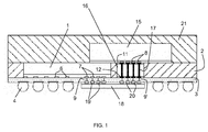
- the package shown in Figure 1 comprises a logic die 1 and a memory die 15 with interconnected arrays of I/O contacts 7/8.
- the memory die 15 may be a DRAM chip configured according to the Wide I/O standard. Both arrays of contacts 7 and 8 are in that case configured according to this standard, i.e. each array comprises 4 banks of 6x73 contact pads at a 40 ⁇ m pitch.
- the invention is however not limited to such devices and the embodiment of Figure 1 is to be understood as merely illustrating a typical field of application of the invention.
- the logic die 1 is embedded in a substrate 2 formed of a mold material and comprising a redistribution layer (RDL) 3 on the front side of the substrate.
- RDL redistribution layer
- Package level solder balls 4 are mounted on contact pads 5 provided on the surface of the RDL 3, for establishing a connection, through the circuitry (not shown) contained in the RDL 3, to contact terminals 6 provided on the front side of the logic die 1.
- the front side of the logic die 1 is furthermore provided with an array of I/O contacts 7 which are connected individually to a corresponding array of I/O contacts 8 on the memory die 15, mounted on the backside of the substrate 2, 'individually' meaning that each contact of one array is connected to a corresponding contact of the other array (this definition of 'individually' is valid throughout this description).
- TSV Through Substrate Via
- the TSV insert 16 may be a silicon die comprising a plurality of metal-filled vias 17 which connect an array of contacts 11 on the back side of the insert 16 to a corresponding array of contacts 12 on the front side of the insert 16. As the insert 16 is embedded in the substrate material, the front and back sides of the insert 16 coincide with the front and back side of the substrate 2.
- the number of vias 17 corresponds to the number of I/O contacts 7 on the logic die 1 as well as to the number of I/O contacts 8 on the memory die 15.
- the I/O contacts 8 on the memory die 15 are directly bonded to the contacts 11 on the back side of the TSV insert 16.
- a lateral connecting device 18 is mounted on the front side of the RDL 3.
- the lateral connecting device 18 comprises two arrays of contacts 19/20 on the same surface of the lateral connecting device 18, each array having the same number of contacts as the arrays 7 and 8 on the logic die 1 and the memory die 15.
- the contacts 19 of the first array are individually connected to corresponding contacts 20 of the second array by circuitry provided in the lateral connecting device 18.
- the contacts 19 of the first array are furthermore connected individually to the I/O contacts 7 on the logic die 1 by circuitry provided in the RDL 3, preferably by vertical conductors 9.
- the contacts 20 of the second array are individually connected to the contacts 12 on the front side of the TSV insert 16 by circuitry provided in the RDL 3, preferably by vertical connections 9'.
- These vertical connections 9/9' are drawn schematically as lines but they can be brought into practice according to known techniques.
- the vertical connections 9/9' consist of a series of via and pad connections designed in the RDL interconnect stack. Typical implementations are stacked via-connections (all vias and pads aligned with the interconnect pad footprint) or stair-case via connections (vias do not align on top of each other but are slightly offset with respect to each other).
- the lateral connecting device 18 and the TSV insert 16 thereby establish an individual connection between the I/O contacts 7 and 8 of the logic die 1 and the memory die 15.
- the memory die 15 is protected by a second layer of mold material 21.
- the lateral connecting device 18 may be a silicon die comprising a number of back end of line layers, for example a power/ground reference layer and a single high-density interconnect layer, for realizing the connection between the first and second array of contacts 19 and 20 on the lateral connecting device.
- Figure 2 illustrates preferred method steps for producing the package of Figure 1 .
- the process is performed at wafer level, i.e. on a wafer comprising a plurality of logic dies 1.
- the logic dies 1 are first attached to a temporary carrier wafer 25 through an adhesive layer 26 ( Fig. 2a ).
- the TSV inserts 16 are placed adjacent to the logic dies 1 ( Fig. 2b ).
- the height of the logic dies 1 is substantially the same as the height of the TSV inserts 16.
- the logic dies 1 and the inserts 16 are then embedded in a mold material 2', preferably by a compression molding technique as known per se in the above described domain of fan-out wafer level package technology ( Fig. 2c ).
- the type of carrier substrate 25 and adhesive layer 26 may be according to known technology applied in FO-WLP.
- the mold material is also preferably a material commonly applied in FO-WLP.
- Such mold materials typically consist of a thermoset polymer material mixed with a large volume fraction of inorganic materials (typically small silica particles) to control the mold material's mechanical properties (Coefficient of thermal expansion and elastic moduli). After setting of the mold material, this material is removed above the level of the logic dies 1 and the inserts 16 by a suitable thinning technique, preferably by grinding, after which the carrier 25 and the adhesive layer 26 are removed by peeling off, yielding the reconstructed substrate 2 consisting of mold material with logic dies 1 and TSV inserts 16 embedded therein, as shown in Fig. 2d .
- a redistribution layer 3 is applied ( Fig. 2e ), equally in accordance with known techniques applied in FO-WLP, preferably applying thin film technology for producing one or more back end of line-type interconnection levels which connect contact terminals 6 on the logic die 1 to contact pads 5 on the upper surface of the RDL 3, onto which the package level solder balls 4 are produced, e.g. this may be ball grid array (BGA) or chip scale package (CSP) type contact structures.
- BGA ball grid array
- CSP chip scale package
- the RDL 3 typically comprises line geometries that are relatively large in terms of thickness, width and spacing. Typical line-width and spacing is in the order of 5 ⁇ m, going down to about 2 ⁇ m by applying state-of-the-art techniques.
- the RDL 3 furthermore comprises individual connections 9 between the array 7 of I/O contacts on the logic dies 1 and a first array of contacts 27 on the surface of the RDL 3, as well as individual connections 9' between the array of contacts 12 on the front side of the TSV inserts 16 and a second array of contacts 28 on the surface of the RDL 3.
- No package level solder balls are applied on the areas comprising the contacts 27/28. At this point, contacts are available to fully test the embedded die 1 and in case of a faulty die, a decision can be made not to assemble additional dies on this particular location of the reconstructed wafer.
- the lateral connecting devices 18 are then mounted onto the RDL 3, preferably by flip-chip technology as known in the art, so that the first and second array of contacts 19/20 on each lateral connecting device 18 are respectively bonded to the first and second array of contacts 27/28 on the surface of the RDL 3.
- the high density TSV insert 16 and the connections via the lateral connecting device 18 to the embedded die 1 can be tested. In case these connections are defective, a decision can be made not to assemble additional devices at this location.
- the memory dies 15 are then mounted on the backside of the package, preferably by flip-chip technology, so that the I/O contacts 8 of the memory dies are bonded to the contacts 11 on the backside of the TSV inserts 16.
- the memory dies 15 may be protected by a second overmold process, wherein a further mold material 21 is applied over the memory dies, as shown in Fig. 2h .
- the substrate 2 may then be singulated to form separate packages of the type shown in Figure 1 .
- the redistribution layer 3 is not always required.
- the lateral connecting device 18 may be bonded directly to the arrays of contacts 7 and 12 on the front side of the logic die 1 and the TSV insert 16 respectively.
- the contacts have been presented as contact pads lying in an outer layer of the devices that are to be bonded by flip-chip technology.
- This is a simplified representation of what may be more complex in reality, as is it is clear to the skilled person.
- the term 'contact' can be a contact pad or a contact bump, depending on how the contacts are to be interconnected to subsequent devices or layers.
- one device may be provided with pads or hollow contact areas, whereas the other side is provided with bumps, or both sides may be provided with bumps.
- the bumps or pads may be built from a plurality of layers. Contacts may be on top of the upper layer instead of embedded therein as presented in the drawings.
- 'contacts' of a first device are 'bonded directly' to 'contacts' of a second device, this means that this assembly was obtained by placing contacts of the first device in direct physical contact with contacts of the second device, to form an electrical connection between the contacts.
- the original contacts of the two bonded devices may no longer be distinguishable as there has been a merger of materials forming the established bond.
- the 'contacts' of the assembled device are thus to be understood as parts of a merged contact structure, one part being attached to the first device, the second part being attached to the second device.
- the feature 'bonded directly' is then to be understood as the feature according to which these parts are connected by a contact structure that is uniform with the 'contacts'.
- the TSV insert 16 and the lateral connecting device 18 may be produced by techniques known for example from Si-interposer technology. A preferred process flow for producing the TSV insert 16 is described hereafter.
- the Cu pillars are not embedded in a polymer or the pillars are embedded in a polymer on only one of the two sides of the insert 16.
- the pillars When the pillars are not embedded they may be bonded for example to hollow bonding pads on contacts of a semiconductor die or on the lateral connecting device 18.
- the lateral connecting device 18 may be produced from a silicon wafer, by producing on said wafer a number of back-end-of-line type layers, such as a power/ground reference layer and a single high-density interconnect layer, and producing the two arrays of contacts 19 and 20 thereon. Afterwards, the wafer may be attached to a temporary carrier and thinned. The wafer may then be diced to form separate lateral connecting devices 18.
- the technology applied for producing the back-end-of-line type layers and the contact arrays on the lateral connecting device 18 may be the known technology for producing similar layers and contacts on an interposer substrate, for example using cost-effective 65nm node processing facilities.
- the lateral connecting device 18 allows to establish connections between very dense arrays of contacts, as encountered in Wide I/O type technology.
- the regular fan-out interconnect technology for packages, as used for producing the redistribution layer 3 is not adequate or requires a large number of layers to realize the interconnection between the logic die 1 and the TSV insert 16.
- the application of the lateral connecting device 18 provides a solution to that problem.
- connections may be realized within the redistribution layer 3 itself.
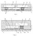
- Figure 3 illustrates an embodiment wherein an additional die is included in the package.
- the third die 30 could be a flash memory die, equally overlapping the logic die 1 and connected thereto via an additional TSV insert 31.
- This second insert 31 comprises less metal-filled vias 32, in agreement with the reduced number of connections between the flash memory die 30 and the logic die 1.
- This reduced number of connections does not require a separate lateral connecting device : connection between the contacts on the front side of the second insert 31 and contact terminals 6 on the logic die 1 can be incorporated in the circuitry of the redistribution layer 3.
- the lateral connecting device 18 is equally embedded in the mold material of the FO-WLP substrate.
- a package according to this embodiment is shown in Figure 4 .
- the logic die 1 is provided with high contact pillars 35 obtainable in a similar manner as described above in relation to the TSV insert 1, however without the step of embedding the pillars in a polymer layer.
- the TSV insert 16 itself and the lateral connecting device 18 are the same as in the previous embodiment.
- the lateral connecting device 18 is now mounted so that its arrays of contacts 19/20 are directly bonded to the arrays of contacts 7 on the logic die 1 and on the front side of the TSV insert 16.
- the high contact pillars 35 are needed because of the location of the lateral connecting device 18, and the pillars must be high enough to allow these pillars 35 and thereby the logic die 1 to be contacted from the front side, despite the presence of the lateral connecting device on said front side.
- the pillars 35 are connected to a redistribution layer 3 and to package level solder balls 4 on said RDL 3, through redistribution circuitry 36 in the RDL 3.
- This embodiment has the advantage that the solder balls 4 need not be interrupted for the placement of the lateral connecting device 18.
- the redistribution circuitry 36 is also present in the RDL 3 shown in Figures 1 to 3 , but it is not shown explicitly in these drawings in order not to overload the figures with details.
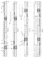
- Figures 5a to 5j illustrate possible process steps for producing the package according to Figure 4 .
- the steps are shown for the production of one single package, but they are preferably performed on wafer level, i.e. for the production of several packages on a single wafer, in analogy with the steps shown in figures 2a-2h .
- the logic die 1 and the TSV insert 16 are attached to a temporary carrier 25 via an adhesive layer 26.
- the lateral connecting device 18 is bonded directly to the logic die 1 and the insert 16 by flip chip bonding, see Figure 5c , i.e.
- the array of contacts 7 on the logic die 1 are directly bonded to the first array of contacts 19 on the lateral connecting device 18 and the array of contacts 12 on the front side of the TSV insert 16 are directly bonded to the second array of contacts 20 on the lateral connecting device 18.
- the height of the lateral connecting device 18 is higher than in the previously described embodiment. Then this assembly of the three devices 1, 16 and 18 is embedded in mold material 2', preferably by compression molding, see
- FIG. 5d followed by planarization through back-grinding, see Figure 5e , until the metal contact pillars 35 of the logic die 1 become exposed.
- the lateral connecting device 18 itself is equally thinned by the back-grinding step. This results in the production of a reconstructed wafer 2 of mold material, with the assembly of the logic die 1, the TSV insert 16 and the (thinned) lateral connecting device 18 embedded therein.
- An alternative to the steps shown in Figures 5d and 5e is to embed the assembly by transfer molding using a film of mold material, in which case the lateral connecting device 18 needs to be at the correct thickness at the time when it is bonded to the TSV insert 16 and the logic die 1.
- a redistribution layer 3 is produced on the reconstructed wafer ( Fig. 5f ), comprising conductors 36 from the metal pillars 35 of the logic die 1 to contact pads 5 on the outer surface of the RDL 3.
- the RDL may be produced in any manner known in FO-WLP technology. At this point, contacts are available to fully test the embedded die 1 and in case of a faulty die, a decision can be made not to assemble additional dies on this particular location of the reconstructed wafer.
- the assembly is then transferred to a second temporary carrier wafer 40 ( Fig. 5g ) and attached thereto via a second adhesive layer 41, after which the first carrier 25 and adhesive layer 26 are removed, exposing the backside of the TSV insert 16 and the logic die 1.
- the memory die 15 is then mounted on said backside by flip-chip bonding, establishing contact between the array of contacts 8 on the memory die and the array of contacts 11 on the backside of the TSV insert 16.
- the memory die 15 is then embedded also in mold material 21 ( Fig. 5h ), after which the second carrier 40 and adhesive layer 41 are removed ( Fig. 5i ) and the package level bumps 4 are applied ( Fig. 5j ).
- process sequences may be devised by the skilled person for the production of the package of Figure 4 .
- the choice of process sequence may influence the number of temporary carriers needed to complete the fabrication process.
- the embodiment of Figure 4 may also be combined with an additional insert 31 with fewer TSVs 32 for connecting a flash memory die 30 to the logic die 1.
- Figure 7 shows an alternative to the embodiments shown in Figures 4 to 6 , having the same advantages of these embodiments.
- the pillars 35 are significantly higher than the thickness of the lateral connecting device 18 and the RDL 3 is not in physical contact with the backside of the lateral connecting device 18.
- the lateral connecting device 18 is mounted on the logic die 1 and the TSV insert 16 prior to the molding step, as in Figure 5c , but the lateral connecting device 18 has already the final thickness at that point, whereas in Figure 5c it has a higher thickness that is afterwards thinned down in the step shown in Figure 5d .
- the description of a layer being present, deposited or produced 'on' another layer or substrate includes the options of
- the description of a device being present, mounted or produced 'on' a surface includes the options of
Landscapes
- Wire Bonding (AREA)
- Semiconductor Integrated Circuits (AREA)
- Internal Circuitry In Semiconductor Integrated Circuit Devices (AREA)
Abstract

Description
- The invention is related to semiconductor processing, in particular to integration of multiple integrated circuit dies in a 3D-interconnected package.
- 3D-integration of integrated circuit devices, also referred to as semiconductor chips or dies, has known many developments in recent years. In particular, the integration of two or more dies with a large number of die-to-die interconnects has become a challenge in terms of the size of the package and the heat dissipation problem. The traditional PoP (Package-on-Package) approach involves the packaging of two dies, for example an application processor in a mobile application and a memory chip, in separate ball-grid array type packages, and assembling one package on top of the other. The resulting package height may be problematic, and package-level solder balls do not allow to realize a large number of interconnections at small pitch, as it is required for example for realizing integration according to the Wide I/O standard.
- One improvement that has been proposed is using an embedded die package or wafer-level reconstructed die package for the bottom die. The embedded die package embeds the silicon die in a laminated PCB. The reconstructed package uses wafer-level molding technology to reconstruct a wafer or panel shaped substrate, which allows for the creation of thin film package-level interconnects in a redistribution layer (RDL). This technology is known as Fan-Out Wafer Level Packaging (FO-WLP) or eWLB, embedded Wafer Level Ball Grid Array, as illustrated for example in document 'Next generation eWLB packaging', Yonggang Jin et al, proceedings of Electronics Packaging Technology Conference (EPTC), 2010.
- In order to enable a package-on-package solution, the FO-WLP approach requires vertical through-package interconnects, connecting the front of the package to the backside. This may be done by laser drilling and filling the holes with Cu or solder to produce through-package vias (TPVs). Another technique uses plating of Cu pillars before die embedding. The obtainable TPV pitch is however rather limited (e.g. TPV-to-TPV pitch not smaller than several 100 µm).
- In order to enable the high bandwidth technology, such as required for Wide I/O DRAM memory, that consists of 4 banks of 6x73 contact pads at a 40µm pitch, a much higher through-package interconnect density is required.
- This can be enabled by direct stacking of the Wide I/O DRAM on the logic die, using through-Si vias in the logic die. This does however require TSVs (Through Silicon Vias, or more generally Through Substrate Vias) in the logic die. Also the thermal coupling between the logic die and the DRAM die is rather high. A different solution is the use of a silicon interposer to realize the high density interconnects using a high density Silicon technology. This allows for lateral placement of the dies (i.e. side by side on the interposer). However the package construction becomes rather expensive. An alternative solution is to remove the package substrate and realize the package as a wafer-level Chip-scale package (CSP). These solutions do however not allow for an independent packaging and easy testing of the logic die.
- The present invention is related to a semiconductor die package and a method for producing the package, as disclosed in the appended claims. A package according to the invention comprises a first die embedded in a reconstructed wafer obtainable by the known FO-WLP or eWLB technologies referred to above. In addition to the first die, placed adjacent to the first die, a Through Substrate Via insert is embedded in the wafer, the TSV insert being a separate element, possibly a silicon die with metal filled vias interconnecting contacts on the front and back sides of the insert. A second die is mounted on the back side of the substrate, with contacts on the second die in electrical connection with the TSV insert's contacts on the back side of the substrate. On the front side of the first die and the TSV insert, a lateral connecting device is mounted which interconnects the TSV insert's contacts on the front side of the substrate to contacts on the front side of the first die. The lateral connecting device and the TSV insert thereby effectively interconnect the contacts on the first and second dies. According to an embodiment, the lateral connecting device is mounted on a redistribution layer (RDL) on the front side of the substrate, as it is known from FO-WLP technology. Package-level solder balls are provided on the RDL, as in known packages, and may be interrupted at the location of the lateral connecting device. According to another embodiment, the lateral connecting device is equally embedded in the reconstructed wafer.
- One of the advantages of the package according to the invention is that testing of the first die can be performed before mounting the second die. In addition, the second die can in many cases be placed to overlap the first die, depending on the location of contacts on the second die. When overlap is possible, this reduces the overall package size as well as the interconnect length when compared to the classic interposer solutions. The TSV inserts and lateral connecting devices can be produced by applying known interposer technology as will be explained in the detailed description. This allows the expensive interposer technology to be limited to smaller dies, leading to a cost reduction in comparison with existing techniques.
- The invention is in particular related to semiconductor die package comprising :
- a substrate formed of a mold material, wherein embedded side by side in said mold material are a first semiconductor die and a Through Substrate Via (TSV) insert, the substrate, the TSV insert and the first die having a front side and a back side, and wherein
- the TSV insert comprises N contacts on the front side of the insert, N contacts on the backside of the insert and N metal-filled vias individually interconnecting said contacts on the front and back sides of the insert, N being an integer higher than or equal to 1,
- the first die comprises N contacts on the front side of the first die,
- the first die further comprises one or more contact terminals on the front side of the first die,
- a second semiconductor die mounted on the back side of the substrate, the second semiconductor die comprising N contacts which are individually connected to the N contacts of the TSV insert on the back side of the insert,
- a lateral connecting device mounted on the front side of the first die and the TSV insert, the lateral connecting device being provided with a first and second group of N contacts each, the groups being placed side by side on the same surface of the lateral connecting device, wherein the first and second group of N contacts are individually interconnected inside the lateral connecting device, and wherein the first and second groups of N contacts on the lateral connecting device are individually connected respectively to the N contacts on the first die and to the N contacts of the TSV insert on the front side of the insert, so that the N contacts on the first die are individually connected to the N contacts on the second die, through the lateral connecting device and the TSV insert,
- a plurality of package level contact bumps connected to at least some of the contact terminals on the first die.
- According to an embodiment, the lateral connecting device is external to the substrate and mounted on the front side of the substrate. In the latter case, the package may further comprise a redistribution layer (RDL) on the front side of the substrate, wherein the package level contact bumps are mounted on the outer surface of said RDL and connected to the contact terminals of the first die through conductors within the RDL, and wherein the lateral connecting device is equally mounted on the outer surface of the RDL.
- The RDL may comprise conductors connecting the N contacts on the first die to a first group of N corresponding contacts on the outer surface of the RDL, the RDL further comprising conductors connecting the N contacts on the front side of the TSV insert to a second group of N corresponding contacts on the outer surface of the RDL, and wherein the first and second group of N contacts on the lateral connecting device are bonded individually respectively to the first and second groups of contacts on the RDL.
- According to an embodiment of the invention, the lateral connecting device is bonded directly to the front side of the first semiconductor die and the TSV insert. In the latter case, the lateral connecting device may equally be embedded in the mold material of the substrate. Still in the latter case, with our without the lateral connecting device embedded in the mold material, the contact terminals of the first die may be contact pillars, the height of which is sufficient for contacting the first die from the front side despite the presence of the lateral connecting device.
- In the latter embodiment, the package may comprise a redistribution layer (RDL) on the front side of the substrate, wherein the package level contact bumps are mounted on the outer surface of said RDL and connected to the contact pillars of the first die through conductors within the RDL. Said RDL may be in direct physical contact with the back side of the lateral connecting device or there may be a layer of mold material between the RDL and the back side of the lateral connecting device.
- A package according to the invention that includes an RDL may further comprise one or more additional semiconductor dies mounted on the back side of the substrate, each additional die being connected to the front side of the substrate by an additional TSV insert and wherein the additional TSV insert is connected to the first semiconductor die by conductors within the RDL.
- According to an embodiment, the lateral connecting device comprises a semiconductor substrate and a back end of line portion, and the interconnection between the first and second group of contacts of the lateral connecting device is established through circuitry in said back end of line portion.
- According to an embodiment, the first semiconductor die is a logic die and the second semiconductor die is a memory die, wherein the N contacts on the first and second dies are formed as dense arrays of I/O contacts.
- According to an embodiment, the N contacts on the second semiconductor die are bonded directly to the N contacts on the back side of the TSV insert.
- The figures are schematic images illustrating the invention, and are not drawn to scale.
-
Figure 1 shows a semiconductor die package according to one embodiment of the invention. -
Figures 2a to 2h illustrate preferred method steps for producing the package ofFig. 1 . -
Figure 3 illustrates an embodiment of a package according to the invention comprising an additional die. -
Figure 4 illustrates a semiconductor package according to another embodiment. -
Figure 5a to 5j shows method steps applicable for producing the package shown inFigure 4 . -
Figure 6 shows the package ofFigure 4 , with an additional die and an additional TSV insert. -
Figure 7 shows an alternative embodiment of the package according to the invention. - The package shown in
Figure 1 comprises alogic die 1 and a memory die 15 with interconnected arrays of I/O contacts 7/8. For example the memory die 15 may be a DRAM chip configured according to the Wide I/O standard. Both arrays ofcontacts Figure 1 is to be understood as merely illustrating a typical field of application of the invention. The logic die 1 is embedded in asubstrate 2 formed of a mold material and comprising a redistribution layer (RDL) 3 on the front side of the substrate. Packagelevel solder balls 4 are mounted oncontact pads 5 provided on the surface of theRDL 3, for establishing a connection, through the circuitry (not shown) contained in theRDL 3, to contactterminals 6 provided on the front side of the logic die 1. The front side of the logic die 1 is furthermore provided with an array of I/O contacts 7 which are connected individually to a corresponding array of I/O contacts 8 on the memory die 15, mounted on the backside of thesubstrate 2, 'individually' meaning that each contact of one array is connected to a corresponding contact of the other array (this definition of 'individually' is valid throughout this description). In addition to the logic die 1, and adjacent to said die, a Through Substrate Via (TSV) insert 16 is embedded in the mold material of thesubstrate 2. The TSV insert 16 may be a silicon die comprising a plurality of metal-filledvias 17 which connect an array ofcontacts 11 on the back side of theinsert 16 to a corresponding array ofcontacts 12 on the front side of theinsert 16. As theinsert 16 is embedded in the substrate material, the front and back sides of theinsert 16 coincide with the front and back side of thesubstrate 2. The number ofvias 17 corresponds to the number of I/O contacts 7 on the logic die 1 as well as to the number of I/O contacts 8 on the memory die 15. - The I/
O contacts 8 on the memory die 15 are directly bonded to thecontacts 11 on the back side of theTSV insert 16. On the front side of theRDL 3, alateral connecting device 18 is mounted. Thelateral connecting device 18 comprises two arrays ofcontacts 19/20 on the same surface of thelateral connecting device 18, each array having the same number of contacts as thearrays contacts 19 of the first array are individually connected to correspondingcontacts 20 of the second array by circuitry provided in thelateral connecting device 18. Thecontacts 19 of the first array are furthermore connected individually to the I/O contacts 7 on the logic die 1 by circuitry provided in theRDL 3, preferably byvertical conductors 9. Likewise, thecontacts 20 of the second array are individually connected to thecontacts 12 on the front side of the TSV insert 16 by circuitry provided in theRDL 3, preferably by vertical connections 9'. Thesevertical connections 9/9' are drawn schematically as lines but they can be brought into practice according to known techniques. Preferably, thevertical connections 9/9' consist of a series of via and pad connections designed in the RDL interconnect stack. Typical implementations are stacked via-connections (all vias and pads aligned with the interconnect pad footprint) or stair-case via connections (vias do not align on top of each other but are slightly offset with respect to each other). Thelateral connecting device 18 and the TSV insert 16 thereby establish an individual connection between the I/O contacts mold material 21. - The
lateral connecting device 18 may be a silicon die comprising a number of back end of line layers, for example a power/ground reference layer and a single high-density interconnect layer, for realizing the connection between the first and second array ofcontacts -
Figure 2 illustrates preferred method steps for producing the package ofFigure 1 . The process is performed at wafer level, i.e. on a wafer comprising a plurality of logic dies 1. The logic dies 1 are first attached to atemporary carrier wafer 25 through an adhesive layer 26 (Fig. 2a ). Following this, the TSV inserts 16 are placed adjacent to the logic dies 1 (Fig. 2b ). The height of the logic dies 1 is substantially the same as the height of the TSV inserts 16. The logic dies 1 and theinserts 16 are then embedded in a mold material 2', preferably by a compression molding technique as known per se in the above described domain of fan-out wafer level package technology (Fig. 2c ). Also the type ofcarrier substrate 25 andadhesive layer 26 may be according to known technology applied in FO-WLP. The mold material is also preferably a material commonly applied in FO-WLP. Such mold materials typically consist of a thermoset polymer material mixed with a large volume fraction of inorganic materials (typically small silica particles) to control the mold material's mechanical properties (Coefficient of thermal expansion and elastic moduli). After setting of the mold material, this material is removed above the level of the logic dies 1 and theinserts 16 by a suitable thinning technique, preferably by grinding, after which thecarrier 25 and theadhesive layer 26 are removed by peeling off, yielding the reconstructedsubstrate 2 consisting of mold material with logic dies 1 and TSV inserts 16 embedded therein, as shown inFig. 2d . - After flipping the substrate, a
redistribution layer 3 is applied (Fig. 2e ), equally in accordance with known techniques applied in FO-WLP, preferably applying thin film technology for producing one or more back end of line-type interconnection levels which connectcontact terminals 6 on the logic die 1 to contactpads 5 on the upper surface of theRDL 3, onto which the packagelevel solder balls 4 are produced, e.g. this may be ball grid array (BGA) or chip scale package (CSP) type contact structures. TheRDL 3 typically comprises line geometries that are relatively large in terms of thickness, width and spacing. Typical line-width and spacing is in the order of 5µm, going down to about 2 µm by applying state-of-the-art techniques. TheRDL 3 furthermore comprisesindividual connections 9 between thearray 7 of I/O contacts on the logic dies 1 and a first array ofcontacts 27 on the surface of theRDL 3, as well as individual connections 9' between the array ofcontacts 12 on the front side of the TSV inserts 16 and a second array ofcontacts 28 on the surface of theRDL 3. No package level solder balls are applied on the areas comprising thecontacts 27/28. At this point, contacts are available to fully test the embeddeddie 1 and in case of a faulty die, a decision can be made not to assemble additional dies on this particular location of the reconstructed wafer. - As shown in
Fig. 2f , thelateral connecting devices 18 are then mounted onto theRDL 3, preferably by flip-chip technology as known in the art, so that the first and second array ofcontacts 19/20 on each lateral connectingdevice 18 are respectively bonded to the first and second array ofcontacts 27/28 on the surface of theRDL 3. At this point the highdensity TSV insert 16 and the connections via thelateral connecting device 18 to the embeddeddie 1 can be tested. In case these connections are defective, a decision can be made not to assemble additional devices at this location. - As shown in
Fig. 2g , the memory dies 15 are then mounted on the backside of the package, preferably by flip-chip technology, so that the I/O contacts 8 of the memory dies are bonded to thecontacts 11 on the backside of the TSV inserts 16. The memory dies 15 may be protected by a second overmold process, wherein afurther mold material 21 is applied over the memory dies, as shown inFig. 2h . Thesubstrate 2 may then be singulated to form separate packages of the type shown inFigure 1 . - Alternatives to the above-described process steps are within the knowledge of the skilled person and may depend on the type of semiconductor dies 1 and 15 that are to be interconnected through the
TSV insert 16 and thelateral connecting device 18. For example, theredistribution layer 3 is not always required. When no RDL is present, thelateral connecting device 18 may be bonded directly to the arrays ofcontacts - In the totality of the attached drawings, and unless stated otherwise, the contacts have been presented as contact pads lying in an outer layer of the devices that are to be bonded by flip-chip technology. This is a simplified representation of what may be more complex in reality, as is it is clear to the skilled person. The term 'contact' can be a contact pad or a contact bump, depending on how the contacts are to be interconnected to subsequent devices or layers. For example one device may be provided with pads or hollow contact areas, whereas the other side is provided with bumps, or both sides may be provided with bumps. The bumps or pads may be built from a plurality of layers. Contacts may be on top of the upper layer instead of embedded therein as presented in the drawings. Another remark regarding the drawings is that the devices have been drawn the same before and after bonding. This is not the case in reality, as flip-chip in many cases involves an underfill step, wherein bonded contacts are embedded in an underfill material after the actual bond has been established. Also, contact pads or bumps will usually undergo a reflow and merge into a single contact structure. The drawings have made abstraction of these details in order not to become over-charged. It is to be noted however, that the bonding of contacts as presented in the drawings and described in this specification may take place according to any method that is applicable in the art known today.
- Also, wherever it is stated in the present description or in the claims that in an assembled device, 'contacts' of a first device are 'bonded directly' to 'contacts' of a second device, this means that this assembly was obtained by placing contacts of the first device in direct physical contact with contacts of the second device, to form an electrical connection between the contacts. In the assembly obtained after bonding, the original contacts of the two bonded devices may no longer be distinguishable as there has been a merger of materials forming the established bond. When this is the case, the 'contacts' of the assembled device are thus to be understood as parts of a merged contact structure, one part being attached to the first device, the second part being attached to the second device. The feature 'bonded directly' is then to be understood as the feature according to which these parts are connected by a contact structure that is uniform with the 'contacts'.
- The TSV insert 16 and the
lateral connecting device 18 may be produced by techniques known for example from Si-interposer technology. A preferred process flow for producing theTSV insert 16 is described hereafter. - 1. Providing a Si wafer
- 2. Deposition of an insulating layer on the wafer, e.g. SiO2 by chemical vapour deposition (CVD)
- 3. Formation of the array of TSV's 17 :
- a. Deposition of photoresist and photopatterning of a TSV pattern.
- b. Etching of the insulating layer and the Si to form deep blind holes in the front side of the Si substrate; e.g. 10 µm diameter and 100 µm deep or 5µm diameter and 50 µm deep.
- c. Deposition of a dielectric layer, conformally covering the sidewalls and bottom of the exposed Si holes and the upper surface of the wafer, with the aim of forming an insulating liner between the TSV and the Si substrate. Typical materials used as liners are Ozone-Teos CVD oxides and plasma-enhanced ALD conformal oxides.
- d. After forming the blind holes and the liner, a Cu barrier layer (e.g. Ti or Ta) is deposited on the walls and bottom of the blind holes and on the upper surface of the wafer, followed by a Cu deposition process by Physical Vapour Deposition (PVD) to form a Cu seed layer on said walls and bottom and upper surface.
- e. Subsequently the holes are filled using Cu electroplating, Cu forming also on the upper surface of the wafer.
- f. After Cu anneal, the plated Cu, the seed Cu and barrier and liner layers are removed from the upper surface of the wafer by CMP processing, resulting in electrically isolated Cu inserts in the top layer of the Si wafer.
- 4. After TSV processing, front side Cu pillars are fabricated on the wafer front side. These Cu pillars will form the
contacts 12 on the front side of the TSV insert. These pillars are e.g. realized using a semi-additive Cu plating process as follows :- a. A Cu plating seed layer is deposited by Physical Vapour Deposition (PVD): e.g. Ti/Cu or TiW/Cu,
- b. A photoresist is deposited and patterned, leaving holes in the locations intended for Cu pillars, the holes covering the isolated Cu inserts in the top layer of the wafer,
- c. Electrolytic deposition of Cu in the open areas of the patterned photoresist,
- d. Stripping of the photoresist,
- e. Back-etching of the PVD Cu seed and the (Ti or TiW) adhesion layer, minimizing the loss of Cu of the much thicker Cu pillars.
- 5. After forming the Cu pillars, the pillars are embedded in a polymer layer. This can e.g. be done by spin-coating or dry film lamination.
- 6. After depositing the polymer layer, the surface of the wafer is planarized, exposing only the tops of the Cu pillars. This can be done through wafer-level grinding, surface planarization or CMP (chemical mechanical polishing) technology,
- 7. The wafer is bonded to a carrier Si wafer using a temporary bonding adhesive layer,
- 8. The backside of the wafer is thinned using mechanical grinding; the wafer is cleaned after grinding,
- 9. The TSVs embedded in the wafer are exposed from the backside. Preferably using a "soft" via-reveal process as follows :
- a. Further thinning of the Si using wet or dry etch techniques. Using an end-point detection system, the thinning is stopped when the tips of the embedded Cu TSV structures are exposed from the wafer backside. The Cu TSVs are still covered with the TSV liner oxide layer.
- b. A backside passivation and insulating layer is deposited (e.g. a stack of SiN and SiO2 layers) A photoresist layer is applied, planarizing the exposed TSV tips.
- c. A dry back-etching step is used to reveal the TSV tips, and using an oxygen-etching chemistry, the tips of the backside passivation and TSV liner are removed, exposing the metal of the TSV (actually the TSV barrier layer, e.g. Ti or Ta).
- 10. Finally, the process used for producing the front-
side Cu pillars 12 is repeated on the backside of the thinned wafer to form theback side pillars 11,resulting in the symmetric TSV insert structure shown infigures 1 to 5 . - 11. The remaining processes include thin wafer debonding from the carrier substrate and transfer to a dicing tape, followed by dicing the wafer to the final individual TSV inserts 16.
- According to an embodiment, the Cu pillars are not embedded in a polymer or the pillars are embedded in a polymer on only one of the two sides of the
insert 16. When the pillars are not embedded they may be bonded for example to hollow bonding pads on contacts of a semiconductor die or on thelateral connecting device 18. - The
lateral connecting device 18 may be produced from a silicon wafer, by producing on said wafer a number of back-end-of-line type layers, such as a power/ground reference layer and a single high-density interconnect layer, and producing the two arrays ofcontacts lateral connecting devices 18. The technology applied for producing the back-end-of-line type layers and the contact arrays on thelateral connecting device 18 may be the known technology for producing similar layers and contacts on an interposer substrate, for example using cost-effective 65nm node processing facilities. - The
lateral connecting device 18 allows to establish connections between very dense arrays of contacts, as encountered in Wide I/O type technology. For such high density interconnects, the regular fan-out interconnect technology for packages, as used for producing theredistribution layer 3, is not adequate or requires a large number of layers to realize the interconnection between the logic die 1 and theTSV insert 16. The application of thelateral connecting device 18 provides a solution to that problem. When the number of interconnects is less dense, connections may be realized within theredistribution layer 3 itself.Figure 3 illustrates an embodiment wherein an additional die is included in the package. In the exemplary case wherein thefirst die 1 is a logic die and thesecond die 15 is a Wide I/O DRAM, thethird die 30 could be a flash memory die, equally overlapping the logic die 1 and connected thereto via anadditional TSV insert 31. Thissecond insert 31 comprises less metal-filledvias 32, in agreement with the reduced number of connections between the flash memory die 30 and the logic die 1. This reduced number of connections does not require a separate lateral connecting device : connection between the contacts on the front side of thesecond insert 31 andcontact terminals 6 on the logic die 1 can be incorporated in the circuitry of theredistribution layer 3. - According to another embodiment, the
lateral connecting device 18 is equally embedded in the mold material of the FO-WLP substrate. A package according to this embodiment is shown inFigure 4 . In this embodiment, the logic die 1 is provided withhigh contact pillars 35 obtainable in a similar manner as described above in relation to theTSV insert 1, however without the step of embedding the pillars in a polymer layer. The TSV insert 16 itself and thelateral connecting device 18 are the same as in the previous embodiment. Thelateral connecting device 18 is now mounted so that its arrays ofcontacts 19/20 are directly bonded to the arrays ofcontacts 7 on the logic die 1 and on the front side of theTSV insert 16. Thehigh contact pillars 35 are needed because of the location of thelateral connecting device 18, and the pillars must be high enough to allow thesepillars 35 and thereby the logic die 1 to be contacted from the front side, despite the presence of the lateral connecting device on said front side. In the embodiment shown, thepillars 35 are connected to aredistribution layer 3 and to packagelevel solder balls 4 on saidRDL 3, throughredistribution circuitry 36 in theRDL 3. This embodiment has the advantage that thesolder balls 4 need not be interrupted for the placement of thelateral connecting device 18. Theredistribution circuitry 36 is also present in theRDL 3 shown inFigures 1 to 3 , but it is not shown explicitly in these drawings in order not to overload the figures with details. -
Figures 5a to 5j illustrate possible process steps for producing the package according toFigure 4 . The steps are shown for the production of one single package, but they are preferably performed on wafer level, i.e. for the production of several packages on a single wafer, in analogy with the steps shown infigures 2a-2h . As seen inFigures 5a-5b , the logic die 1 and theTSV insert 16 are attached to atemporary carrier 25 via anadhesive layer 26. Then thelateral connecting device 18 is bonded directly to the logic die 1 and theinsert 16 by flip chip bonding, seeFigure 5c , i.e. the array ofcontacts 7 on the logic die 1 are directly bonded to the first array ofcontacts 19 on thelateral connecting device 18 and the array ofcontacts 12 on the front side of theTSV insert 16 are directly bonded to the second array ofcontacts 20 on thelateral connecting device 18. The height of thelateral connecting device 18 is higher than in the previously described embodiment. Then this assembly of the threedevices -
Figure 5d , followed by planarization through back-grinding, seeFigure 5e , until themetal contact pillars 35 of the logic die 1 become exposed. Thelateral connecting device 18 itself is equally thinned by the back-grinding step. This results in the production of areconstructed wafer 2 of mold material, with the assembly of the logic die 1, theTSV insert 16 and the (thinned)lateral connecting device 18 embedded therein. An alternative to the steps shown inFigures 5d and5e is to embed the assembly by transfer molding using a film of mold material, in which case thelateral connecting device 18 needs to be at the correct thickness at the time when it is bonded to theTSV insert 16 and the logic die 1. - Then a
redistribution layer 3 is produced on the reconstructed wafer (Fig. 5f ), comprisingconductors 36 from themetal pillars 35 of the logic die 1 to contactpads 5 on the outer surface of theRDL 3. The RDL may be produced in any manner known in FO-WLP technology. At this point, contacts are available to fully test the embeddeddie 1 and in case of a faulty die, a decision can be made not to assemble additional dies on this particular location of the reconstructed wafer. The assembly is then transferred to a second temporary carrier wafer 40 (Fig. 5g ) and attached thereto via a secondadhesive layer 41, after which thefirst carrier 25 andadhesive layer 26 are removed, exposing the backside of theTSV insert 16 and the logic die 1. At this point the highdensity TSV insert 16 and the connections via thelateral connecting device 18 to the embeddeddie 1 can be tested. In case these connections are defective, a decision can be made not to assemble additional devices at this location. As seen still inFigure 5g , the memory die 15 is then mounted on said backside by flip-chip bonding, establishing contact between the array ofcontacts 8 on the memory die and the array ofcontacts 11 on the backside of theTSV insert 16. The memory die 15 is then embedded also in mold material 21 (Fig. 5h ), after which thesecond carrier 40 andadhesive layer 41 are removed (Fig. 5i ) and the package level bumps 4 are applied (Fig. 5j ). - Other process sequences may be devised by the skilled person for the production of the package of
Figure 4 . For example, it is possible also to first place thelateral connecting device 18 on a first temporary carrier, followed by flip-chip bonding of theTSV insert 16 and the logic die 1 to thelateral connecting device 18. This is then followed by embedding the assembly of thelateral connecting device 18, theTSV insert 16 and the logic die 1 in mold material by compression molding or transfer molding, and producing theRDL 3 and package level bumps 4. The choice of process sequence may influence the number of temporary carriers needed to complete the fabrication process. - As shown in
Figure 6 , the embodiment ofFigure 4 may also be combined with anadditional insert 31 withfewer TSVs 32 for connecting a flash memory die 30 to the logic die 1. -
Figure 7 shows an alternative to the embodiments shown inFigures 4 to 6 , having the same advantages of these embodiments. In the assembly ofFigure 7 , thepillars 35 are significantly higher than the thickness of thelateral connecting device 18 and theRDL 3 is not in physical contact with the backside of thelateral connecting device 18. In the process sequence for producing such a package, thelateral connecting device 18 is mounted on the logic die 1 and theTSV insert 16 prior to the molding step, as inFigure 5c , but thelateral connecting device 18 has already the final thickness at that point, whereas inFigure 5c it has a higher thickness that is afterwards thinned down in the step shown inFigure 5d . In the alternative process, thinning down of the polymer 2' takes place until the (higher)pillars 35 are exposed. At that point, a layer of polymer 2' is still present on the backside of thelateral connecting device 18. TheRDL 3 is then produced on the planarized surface, in the same way as shown inFigure 5f and completion of the package also takes place in the manner shown inFigures 5g to 5j . - While the invention has been illustrated and described in detail in the drawings and foregoing description, such illustration and description are to be considered illustrative or exemplary and not restrictive. Other variations to the disclosed embodiments can be understood and effected by those skilled in the art in practicing the claimed invention, from a study of the drawings, the disclosure and the appended claims. In the claims, the word "comprising" does not exclude other elements or steps, and the indefinite article "a" or "an" does not exclude a plurality. The mere fact that certain measures are recited in mutually different dependent claims does not indicate that a combination of these measures cannot be used to advantage. Any reference signs in the claims should not be construed as limiting the scope.
- Unless specifically specified, the description of a layer being present, deposited or produced 'on' another layer or substrate, includes the options of
- said layer being present, produced or deposited directly on, i.e. in physical contact with, said other layer or substrate, and
- said layer being present, produced or deposited on one or a stack of intermediate layers between said layer and said other layer or substrate.
- Unless specifically specified, the description of a device being present, mounted or produced 'on' a surface, includes the options of
- said device being present, mounted or produced directly on, i.e. in physical contact with said surface, and
- said device being present, mounted or produced on one or a stack of intermediate layers between said surface and said device.
Claims (14)
- A semiconductor die package comprising :• a substrate (2) formed of a mold material, wherein embedded side by side in said mold material are a first semiconductor die (1) and a Through Substrate Via (TSV) insert (16), the substrate (2), the TSV insert (16) and the first die (1) having a front side and a back side, and wherein• the TSV insert (16) comprises N contacts (12) on the front side of the insert, N contacts (11) on the backside of the insert and N metal-filled vias (17) individually interconnecting said contacts (12,11) on the front and back sides of the insert, N being an integer higher than or equal to 1,• the first die (1) comprises N contacts (7) on the front side of the first die,• the first die further comprises one or more contact terminals (6,35) on the front side of the first die,• a second semiconductor die (15) mounted on the back side of the substrate (2), the second semiconductor die comprising N contacts (8) which are individually connected to the N contacts (11) of the TSV insert (16) on the back side of the insert (16),• a lateral connecting device (18) mounted on the front side of the first die (1) and the TSV insert (16), the lateral connecting device being provided with a first and second group (19,20) of N contacts each, the groups being placed side by side on the same surface of the lateral connecting device, wherein the first and second group (19,20) of N contacts are individually interconnected inside the lateral connecting device, and wherein the first and second groups (19,20) of N contacts on the lateral connecting device are individually connected respectively to the N contacts (7) on the first die and to the N contacts (12) of the TSV insert (16) on the front side of the insert, so that the N contacts (7) on the first die (1) are individually connected to the N contacts (8) on the second die (15), through the lateral connecting device (18) and the TSV insert (16),• a plurality of package level contact bumps (4) connected to at least some of the contact terminals (6) on the first die.
- The package according to claim 1, wherein the lateral connecting device (18) is external to the substrate (2) and mounted on the front side of the substrate (2).
- The package according to claim 2, comprising a redistribution layer (RDL) (3) on the front side of the substrate (2), and wherein the package level contact bumps (4) are mounted on the outer surface of said RDL (3) and connected to the contact terminals of the first die (1) through conductors (36) within the RDL (3), and wherein the lateral connecting device (18) is equally mounted on the outer surface of the RDL (3).
- The package according to claim 3, wherein the RDL (3) comprises conductors (9) connecting the N contacts (7) on the first die (1) to a first group of N corresponding contacts (27) on the outer surface of the RDL (3), the RDL (3) further comprising conductors (9') connecting the N contacts (12) on the front side of the TSV insert (16) to a second group of N corresponding contacts (28) on the outer surface of the RDL, and wherein the first and second group of N contacts (19,20) on the lateral connecting device (18) are bonded individually respectively to the first and second groups of contacts (27,28) on the RDL (3).
- The package according to claim 1, wherein the lateral connecting device (18) is bonded directly to the front side of the first semiconductor die (1) and the TSV insert (16).
- The package according to claim 5, wherein the lateral connecting device (18) is equally embedded in the mold material of the substrate (2).
- The package according to claim 5 or 6, wherein the contact terminals of the first die are contact pillars (35), the height of which is sufficient for contacting the first die (1) from the front side despite the presence of the lateral connecting device (18).
- The package according to claim 7, comprising a redistribution layer (RDL) (3) on the front side of the substrate (2), and wherein the package level contact bumps (4) are mounted on the outer surface of said RDL (3) and connected to the contact pillars (35) of the first die (1) through conductors (36) within the RDL (3).
- The package according to claim 8, wherein the RDL (3) is in direct physical contact with the back side of the lateral connecting device (18).
- The package according to claim 8, wherein a layer of mold material is present between the RDL (3) and the back side of the lateral connecting device (18).
- The package according to claim 3, 4 or 8 to 10, comprising one or more additional semiconductor dies (31) mounted on the back side of the substrate (2), each additional die being connected to the front side of the substrate by an additional TSV insert (32) and wherein the additional TSV insert is connected to the first semiconductor die (1) by conductors within the RDL (3).
- The package according to any one of the preceding claims, wherein the lateral connecting device (18) comprises a semiconductor substrate and a back end of line portion, and wherein the interconnection between the first and second group of contacts (19,20) of the lateral connecting device (18) is established through circuitry in said back end of line portion.
- The package according to any one of the preceding claims, wherein the first semiconductor die is a logic die (1) and wherein the second semiconductor die is a memory die (15) and wherein the N contacts (7,8) on the first and second dies are formed as dense arrays of I/O contacts.
- The package according to any one of the preceding claims, wherein the N contacts (8) on the second semiconductor die (15) are bonded directly to the N contacts (11) on the back side of the TSV insert (16).
Priority Applications (3)
| Application Number | Priority Date | Filing Date | Title |
|---|---|---|---|
| EP16185640.6A EP3288076B1 (en) | 2016-08-25 | 2016-08-25 | A semiconductor die package and method of producing the package |
| US15/686,015 US9966325B2 (en) | 2016-08-25 | 2017-08-24 | Semiconductor die package and method of producing the package |
| CN201710735129.0A CN107785358B (en) | 2016-08-25 | 2017-08-24 | Semiconductor die package and method of producing such a package |
Applications Claiming Priority (1)
| Application Number | Priority Date | Filing Date | Title |
|---|---|---|---|
| EP16185640.6A EP3288076B1 (en) | 2016-08-25 | 2016-08-25 | A semiconductor die package and method of producing the package |
Publications (2)
| Publication Number | Publication Date |
|---|---|
| EP3288076A1 true EP3288076A1 (en) | 2018-02-28 |
| EP3288076B1 EP3288076B1 (en) | 2021-06-23 |
Family
ID=56801426
Family Applications (1)
| Application Number | Title | Priority Date | Filing Date |
|---|---|---|---|
| EP16185640.6A Active EP3288076B1 (en) | 2016-08-25 | 2016-08-25 | A semiconductor die package and method of producing the package |
Country Status (3)
| Country | Link |
|---|---|
| US (1) | US9966325B2 (en) |
| EP (1) | EP3288076B1 (en) |
| CN (1) | CN107785358B (en) |
Cited By (6)
| Publication number | Priority date | Publication date | Assignee | Title |
|---|---|---|---|---|
| WO2019209634A1 (en) * | 2018-04-24 | 2019-10-31 | Cisco Technology, Inc. | Integrated circuit bridge for photonics and electrical chip integration |
| EP3640979A1 (en) * | 2018-10-15 | 2020-04-22 | IMEC vzw | A method for packaging semiconductor dies |
| EP3644359A1 (en) * | 2018-10-23 | 2020-04-29 | AT & S Austria Technologie & Systemtechnik Aktiengesellschaft | Z-axis interconnection with protruding component |
| EP3671833A1 (en) | 2018-12-20 | 2020-06-24 | IMEC vzw | A method for packaging semiconductor dies |
| WO2020176313A1 (en) * | 2019-02-27 | 2020-09-03 | Apple Inc. | High bandwidth die to die interconnect with package area reduction |
| US12154861B2 (en) * | 2019-10-31 | 2024-11-26 | Texas Instruments Incorporated | Frame design in embedded die package |
Families Citing this family (63)
| Publication number | Priority date | Publication date | Assignee | Title |
|---|---|---|---|---|
| US9136236B2 (en) | 2012-09-28 | 2015-09-15 | Intel Corporation | Localized high density substrate routing |
| US9190380B2 (en) | 2012-12-06 | 2015-11-17 | Intel Corporation | High density substrate routing in BBUL package |
| WO2017188951A1 (en) | 2016-04-28 | 2017-11-02 | Intel Corporation | Integrated circuit structures with extended conductive pathways |
| US10204893B2 (en) | 2016-05-19 | 2019-02-12 | Invensas Bonding Technologies, Inc. | Stacked dies and methods for forming bonded structures |
| US10366968B2 (en) * | 2016-09-30 | 2019-07-30 | Intel IP Corporation | Interconnect structure for a microelectronic device |
| US11625523B2 (en) | 2016-12-14 | 2023-04-11 | iCometrue Company Ltd. | Logic drive based on standard commodity FPGA IC chips |
| US10489544B2 (en) | 2016-12-14 | 2019-11-26 | iCometrue Company Ltd. | Logic drive based on standard commodity FPGA IC chips |
| US10447274B2 (en) | 2017-07-11 | 2019-10-15 | iCometrue Company Ltd. | Logic drive based on standard commodity FPGA IC chips using non-volatile memory cells |
| US10957679B2 (en) | 2017-08-08 | 2021-03-23 | iCometrue Company Ltd. | Logic drive based on standardized commodity programmable logic semiconductor IC chips |
| US10630296B2 (en) | 2017-09-12 | 2020-04-21 | iCometrue Company Ltd. | Logic drive with brain-like elasticity and integrality based on standard commodity FPGA IC chips using non-volatile memory cells |
| US10529693B2 (en) * | 2017-11-29 | 2020-01-07 | Advanced Micro Devices, Inc. | 3D stacked dies with disparate interconnect footprints |
| US10608642B2 (en) | 2018-02-01 | 2020-03-31 | iCometrue Company Ltd. | Logic drive using standard commodity programmable logic IC chips comprising non-volatile radom access memory cells |
| US10623000B2 (en) | 2018-02-14 | 2020-04-14 | iCometrue Company Ltd. | Logic drive using standard commodity programmable logic IC chips |
| US11276676B2 (en) | 2018-05-15 | 2022-03-15 | Invensas Bonding Technologies, Inc. | Stacked devices and methods of fabrication |
| US10608638B2 (en) | 2018-05-24 | 2020-03-31 | iCometrue Company Ltd. | Logic drive using standard commodity programmable logic IC chips |
| US12476637B2 (en) | 2018-05-24 | 2025-11-18 | iCometrue Company Ltd. | Logic drive using standard commodity programmable logic IC chips |
| US10727204B2 (en) | 2018-05-29 | 2020-07-28 | Advances Micro Devices, Inc. | Die stacking for multi-tier 3D integration |
| US10937755B2 (en) | 2018-06-29 | 2021-03-02 | Advanced Micro Devices, Inc. | Bond pads for low temperature hybrid bonding |
| WO2020010136A1 (en) | 2018-07-06 | 2020-01-09 | Invensas Bonding Technologies, Inc. | Molded direct bonded and interconnected stack |
| WO2020010265A1 (en) | 2018-07-06 | 2020-01-09 | Invensas Bonding Technologies, Inc. | Microelectronic assemblies |
| US10892011B2 (en) | 2018-09-11 | 2021-01-12 | iCometrue Company Ltd. | Logic drive using standard commodity programmable logic IC chips comprising non-volatile random access memory cells |
| US11309334B2 (en) | 2018-09-11 | 2022-04-19 | iCometrue Company Ltd. | Logic drive using standard commodity programmable logic IC chips comprising non-volatile random access memory cells |
| US10937762B2 (en) | 2018-10-04 | 2021-03-02 | iCometrue Company Ltd. | Logic drive based on multichip package using interconnection bridge |
| US11616046B2 (en) | 2018-11-02 | 2023-03-28 | iCometrue Company Ltd. | Logic drive based on chip scale package comprising standardized commodity programmable logic IC chip and memory IC chip |
| US11211334B2 (en) | 2018-11-18 | 2021-12-28 | iCometrue Company Ltd. | Logic drive based on chip scale package comprising standardized commodity programmable logic IC chip and memory IC chip |
| CN112219276A (en) * | 2018-11-23 | 2021-01-12 | 华为技术有限公司 | A chip and chip packaging method |
| CN113330557A (en) | 2019-01-14 | 2021-08-31 | 伊文萨思粘合技术公司 | Bonding structure |
| US10833051B2 (en) * | 2019-01-24 | 2020-11-10 | International Business Machines Corporation | Precision alignment of multi-chip high density interconnects |
| TWI810380B (en) * | 2019-02-22 | 2023-08-01 | 南韓商愛思開海力士有限公司 | System-in-packages including a bridge die |
| US10803548B2 (en) | 2019-03-15 | 2020-10-13 | Intel Corporation | Disaggregation of SOC architecture |
| US11056453B2 (en) | 2019-06-18 | 2021-07-06 | Deca Technologies Usa, Inc. | Stackable fully molded semiconductor structure with vertical interconnects |
| US11296053B2 (en) | 2019-06-26 | 2022-04-05 | Invensas Bonding Technologies, Inc. | Direct bonded stack structures for increased reliability and improved yield in microelectronics |
| US11227838B2 (en) | 2019-07-02 | 2022-01-18 | iCometrue Company Ltd. | Logic drive based on multichip package comprising standard commodity FPGA IC chip with cooperating or supporting circuits |
| US10985154B2 (en) | 2019-07-02 | 2021-04-20 | iCometrue Company Ltd. | Logic drive based on multichip package comprising standard commodity FPGA IC chip with cryptography circuits |
| US11887930B2 (en) | 2019-08-05 | 2024-01-30 | iCometrue Company Ltd. | Vertical interconnect elevator based on through silicon vias |
| TW202109800A (en) * | 2019-08-15 | 2021-03-01 | 力成科技股份有限公司 | Fan-out chip package and fan-out bottom package with fine pitch silicon through via |
| US11637056B2 (en) | 2019-09-20 | 2023-04-25 | iCometrue Company Ltd. | 3D chip package based on through-silicon-via interconnection elevator |
| DE102020106799A1 (en) | 2019-09-20 | 2021-03-25 | Taiwan Semiconductor Manufacturing Co., Ltd. | SEMICONDUCTOR COMPONENTS AND METHOD OF MANUFACTURING |
| US11856800B2 (en) | 2019-09-20 | 2023-12-26 | Taiwan Semiconductor Manufacturing Company, Ltd. | Semiconductor devices with system on chip devices |
| CN118888563A (en) * | 2019-10-09 | 2024-11-01 | 财团法人工业技术研究院 | Multi-chip package and method of manufacturing the same |
| US11587905B2 (en) | 2019-10-09 | 2023-02-21 | Industrial Technology Research Institute | Multi-chip package and manufacturing method thereof |
| TWI759844B (en) * | 2019-10-09 | 2022-04-01 | 財團法人工業技術研究院 | Multi-chip package and manufacture method thereof |
| TWI701777B (en) * | 2019-10-22 | 2020-08-11 | 財團法人工業技術研究院 | Image sensor package and manufacture method thereof |
| US20210134690A1 (en) * | 2019-11-01 | 2021-05-06 | Advanced Semiconductor Engineering, Inc. | Semiconductor device packages and methods of manufacturing the same |
| US11735564B2 (en) * | 2019-12-04 | 2023-08-22 | Sj Semiconductor (Jiangyin) Corporation | Three-dimensional chip packaging structure and method thereof |
| CN113013125B (en) * | 2019-12-20 | 2024-07-09 | 奥特斯奥地利科技与系统技术有限公司 | Component carrier with embedded interposer laterally located between electrically conductive structures of a stack |
| US11309283B2 (en) | 2019-12-31 | 2022-04-19 | Powertech Technology Inc. | Packaging structure and manufacturing method thereof |
| TWI768294B (en) * | 2019-12-31 | 2022-06-21 | 力成科技股份有限公司 | Package structure and manufacturing method thereof |
| US11600526B2 (en) | 2020-01-22 | 2023-03-07 | iCometrue Company Ltd. | Chip package based on through-silicon-via connector and silicon interconnection bridge |
| KR102746859B1 (en) | 2020-01-23 | 2024-12-27 | 삼성전자주식회사 | Semiconductor package and manufacturing method thereof |
| US11631647B2 (en) | 2020-06-30 | 2023-04-18 | Adeia Semiconductor Bonding Technologies Inc. | Integrated device packages with integrated device die and dummy element |
| TW202240808A (en) | 2021-01-08 | 2022-10-16 | 成真股份有限公司 | Micro heat pipes for use in integrated circuit chip package |
| US12176278B2 (en) | 2021-05-30 | 2024-12-24 | iCometrue Company Ltd. | 3D chip package based on vertical-through-via connector |
| CN113035858B (en) * | 2021-05-31 | 2021-09-14 | 杭州光智元科技有限公司 | Semiconductor device and method for manufacturing the same |
| US11728248B2 (en) | 2021-07-01 | 2023-08-15 | Deca Technologies Usa, Inc. | Fully molded semiconductor structure with through silicon via (TSV) vertical interconnects |
| US11616003B2 (en) * | 2021-07-01 | 2023-03-28 | Deca Technologies Usa, Inc. | Stackable fully molded semiconductor structure with through silicon via (TSV) vertical interconnects |
| KR20230032587A (en) * | 2021-08-31 | 2023-03-07 | 삼성전자주식회사 | Semiconductor package |
| US12555628B2 (en) | 2021-09-24 | 2026-02-17 | iCometrue Company Ltd. | Multi-output look-up table (LUT) for use in coarse-grained field-programmable-gate-array (FPGA) integrated-circuit (IC) chip |
| US12268012B2 (en) | 2021-09-24 | 2025-04-01 | iCometrue Company Ltd. | Multi-output look-up table (LUT) for use in coarse-grained field-programmable-gate-array (FPGA) integrated-circuit (IC) chip |
| US12604766B2 (en) | 2021-10-22 | 2026-04-14 | Mediatek Inc. | Semiconductor package structure |
| FR3133705B1 (en) * | 2022-03-17 | 2025-03-07 | St Microelectronics Crolles 2 Sas | Electronic device |
| TWI824688B (en) * | 2022-08-31 | 2023-12-01 | 晶呈科技股份有限公司 | Bonding and transfer methods of chip packages |
| US12593732B2 (en) * | 2022-12-01 | 2026-03-31 | Taiwan Semiconductor Manufacturing Company, Ltd. | Semiconductor device and manufacturing method thereof |
Citations (4)
| Publication number | Priority date | Publication date | Assignee | Title |
|---|---|---|---|---|
| WO2012012338A1 (en) * | 2010-07-20 | 2012-01-26 | Marvell World Trad Ltd. | Embedded structures and methods of manufacture thereof |
| US20140103527A1 (en) * | 2012-03-23 | 2014-04-17 | Stats Chippac, Ltd. | Semiconductor Device and Method of Forming a POP Device with Embedded Vertical Interconnect Units |
| US20140264836A1 (en) * | 2013-03-15 | 2014-09-18 | Qualcomm Incorporated | System-in-package with interposer pitch adapter |
| US20170062384A1 (en) * | 2015-09-02 | 2017-03-02 | SK Hynix Inc. | Semiconductor package embedded with plurality of chips and method of manufacturing the same |
Family Cites Families (10)
| Publication number | Priority date | Publication date | Assignee | Title |
|---|---|---|---|---|
| US7098542B1 (en) | 2003-11-07 | 2006-08-29 | Xilinx, Inc. | Multi-chip configuration to connect flip-chips to flip-chips |
| US20080157316A1 (en) | 2007-01-03 | 2008-07-03 | Advanced Chip Engineering Technology Inc. | Multi-chips package and method of forming the same |
| US8064224B2 (en) | 2008-03-31 | 2011-11-22 | Intel Corporation | Microelectronic package containing silicon patches for high density interconnects, and method of manufacturing same |
| US8227904B2 (en) | 2009-06-24 | 2012-07-24 | Intel Corporation | Multi-chip package and method of providing die-to-die interconnects in same |
| US9230898B2 (en) | 2009-08-17 | 2016-01-05 | Stats Chippac Ltd. | Integrated circuit packaging system with package-on-package and method of manufacture thereof |
| KR101918608B1 (en) * | 2012-02-28 | 2018-11-14 | 삼성전자 주식회사 | Semiconductor package |
| US8872349B2 (en) | 2012-09-11 | 2014-10-28 | Intel Corporation | Bridge interconnect with air gap in package assembly |
| US9236366B2 (en) * | 2012-12-20 | 2016-01-12 | Intel Corporation | High density organic bridge device and method |
| US8901748B2 (en) | 2013-03-14 | 2014-12-02 | Intel Corporation | Direct external interconnect for embedded interconnect bridge package |
| US9041205B2 (en) * | 2013-06-28 | 2015-05-26 | Intel Corporation | Reliable microstrip routing for electronics components |
-
2016
- 2016-08-25 EP EP16185640.6A patent/EP3288076B1/en active Active
-
2017
- 2017-08-24 CN CN201710735129.0A patent/CN107785358B/en active Active
- 2017-08-24 US US15/686,015 patent/US9966325B2/en active Active
Patent Citations (4)
| Publication number | Priority date | Publication date | Assignee | Title |
|---|---|---|---|---|
| WO2012012338A1 (en) * | 2010-07-20 | 2012-01-26 | Marvell World Trad Ltd. | Embedded structures and methods of manufacture thereof |
| US20140103527A1 (en) * | 2012-03-23 | 2014-04-17 | Stats Chippac, Ltd. | Semiconductor Device and Method of Forming a POP Device with Embedded Vertical Interconnect Units |
| US20140264836A1 (en) * | 2013-03-15 | 2014-09-18 | Qualcomm Incorporated | System-in-package with interposer pitch adapter |
| US20170062384A1 (en) * | 2015-09-02 | 2017-03-02 | SK Hynix Inc. | Semiconductor package embedded with plurality of chips and method of manufacturing the same |
Non-Patent Citations (1)
| Title |
|---|
| YONGGANG JIN ET AL.: "Next generation eWLB packaging", ELECTRONICS PACKAGING TECHNOLOGY CONFERENCE (EPTC, 2010 |
Cited By (15)
| Publication number | Priority date | Publication date | Assignee | Title |
|---|---|---|---|---|
| US11043478B2 (en) | 2018-04-24 | 2021-06-22 | Cisco Technology, Inc. | Integrated circuit bridge for photonics and electrical chip integration |
| WO2019209634A1 (en) * | 2018-04-24 | 2019-10-31 | Cisco Technology, Inc. | Integrated circuit bridge for photonics and electrical chip integration |
| EP3640979A1 (en) * | 2018-10-15 | 2020-04-22 | IMEC vzw | A method for packaging semiconductor dies |
| EP3644359A1 (en) * | 2018-10-23 | 2020-04-29 | AT & S Austria Technologie & Systemtechnik Aktiengesellschaft | Z-axis interconnection with protruding component |
| US11864319B2 (en) | 2018-10-23 | 2024-01-02 | AT&SAustria Technologie &Systemtechnik AG | Z-axis interconnection with protruding component |
| US11367705B2 (en) | 2018-12-20 | 2022-06-21 | Imec Vzw | Method for packaging semiconductor dies |
| EP3671833A1 (en) | 2018-12-20 | 2020-06-24 | IMEC vzw | A method for packaging semiconductor dies |
| US20210020610A1 (en) * | 2019-02-27 | 2021-01-21 | Apple Inc. | High bandwidth die to die interconnect with package area reduction |
| US10770433B1 (en) | 2019-02-27 | 2020-09-08 | Apple Inc. | High bandwidth die to die interconnect with package area reduction |
| CN113498549A (en) * | 2019-02-27 | 2021-10-12 | 苹果公司 | High bandwidth die-to-die interconnect with reduced package area |
| WO2020176313A1 (en) * | 2019-02-27 | 2020-09-03 | Apple Inc. | High bandwidth die to die interconnect with package area reduction |
| US11587909B2 (en) * | 2019-02-27 | 2023-02-21 | Apple Inc. | High bandwidth die to die interconnect with package area reduction |
| US12368137B2 (en) | 2019-02-27 | 2025-07-22 | Apple Inc. | High bandwidth die to die interconnect with package area reduction |
| CN113498549B (en) * | 2019-02-27 | 2025-11-11 | 苹果公司 | High bandwidth die-to-die interconnect with reduced package area |
| US12154861B2 (en) * | 2019-10-31 | 2024-11-26 | Texas Instruments Incorporated | Frame design in embedded die package |
Also Published As
| Publication number | Publication date |
|---|---|
| CN107785358A (en) | 2018-03-09 |
| CN107785358B (en) | 2023-05-26 |
| EP3288076B1 (en) | 2021-06-23 |
| US20180061741A1 (en) | 2018-03-01 |
| US9966325B2 (en) | 2018-05-08 |
Similar Documents
| Publication | Publication Date | Title |
|---|---|---|
| US9966325B2 (en) | Semiconductor die package and method of producing the package | |
| US12020997B2 (en) | Methods of forming semiconductor device packages having alignment marks on a carrier substrate | |
| US12218089B2 (en) | Packaged semiconductor device and method of forming thereof | |
| US11527465B2 (en) | Packages with Si-substrate-free interposer and method forming same | |
| CN112242367A (en) | Package structure and method of forming the same | |
| KR20220102542A (en) | Semiconductor package and method of manufacturing semiconductor package | |
| KR20180114491A (en) | Packages with si-substrate-free interposer and method forming same | |
| US11367705B2 (en) | Method for packaging semiconductor dies | |
| CN112582389B (en) | Semiconductor package, package and method of forming the same | |
| KR102485701B1 (en) | Semiconductor device and method | |
| US12588482B2 (en) | Method for forming semiconductor redistribution structures | |
| US20250349691A1 (en) | Semiconductor device and method | |
| US20250343074A1 (en) | Semiconductor device and method | |
| US12616017B2 (en) | Semiconductor device and method | |
| CN221747211U (en) | Integrated Circuit Packaging | |
| CN223108879U (en) | Semiconductor devices | |
| US20250349774A1 (en) | Semiconductor device and method | |
| CN119153434A (en) | Semiconductor device and method of forming the same |
Legal Events
| Date | Code | Title | Description |
|---|---|---|---|
| PUAI | Public reference made under article 153(3) epc to a published international application that has entered the european phase |
Free format text: ORIGINAL CODE: 0009012 |
|
| STAA | Information on the status of an ep patent application or granted ep patent |
Free format text: STATUS: THE APPLICATION HAS BEEN PUBLISHED |
|
| AK | Designated contracting states |
Kind code of ref document: A1 Designated state(s): AL AT BE BG CH CY CZ DE DK EE ES FI FR GB GR HR HU IE IS IT LI LT LU LV MC MK MT NL NO PL PT RO RS SE SI SK SM TR |
|
| AX | Request for extension of the european patent |
Extension state: BA ME |
|
| STAA | Information on the status of an ep patent application or granted ep patent |
Free format text: STATUS: REQUEST FOR EXAMINATION WAS MADE |
|
| 17P | Request for examination filed |
Effective date: 20180807 |
|
| RBV | Designated contracting states (corrected) |
Designated state(s): AL AT BE BG CH CY CZ DE DK EE ES FI FR GB GR HR HU IE IS IT LI LT LU LV MC MK MT NL NO PL PT RO RS SE SI SK SM TR |
|
| STAA | Information on the status of an ep patent application or granted ep patent |
Free format text: STATUS: EXAMINATION IS IN PROGRESS |
|
| 17Q | First examination report despatched |
Effective date: 20200826 |
|
| GRAP | Despatch of communication of intention to grant a patent |
Free format text: ORIGINAL CODE: EPIDOSNIGR1 |
|
| STAA | Information on the status of an ep patent application or granted ep patent |
Free format text: STATUS: GRANT OF PATENT IS INTENDED |
|
| RIC1 | Information provided on ipc code assigned before grant |
Ipc: H01L 23/538 20060101AFI20210316BHEP Ipc: H01L 21/60 20060101ALI20210316BHEP Ipc: H01L 25/065 20060101ALI20210316BHEP Ipc: H01L 21/56 20060101ALN20210316BHEP Ipc: H01L 23/31 20060101ALN20210316BHEP |
|
| RIC1 | Information provided on ipc code assigned before grant |
Ipc: H01L 23/538 20060101AFI20210408BHEP Ipc: H01L 21/60 20060101ALI20210408BHEP Ipc: H01L 25/065 20060101ALI20210408BHEP Ipc: H01L 21/56 20060101ALN20210408BHEP Ipc: H01L 23/31 20060101ALN20210408BHEP |
|
| GRAS | Grant fee paid |
Free format text: ORIGINAL CODE: EPIDOSNIGR3 |
|
| INTG | Intention to grant announced |
Effective date: 20210420 |
|
| GRAA | (expected) grant |
Free format text: ORIGINAL CODE: 0009210 |
|
| STAA | Information on the status of an ep patent application or granted ep patent |
Free format text: STATUS: THE PATENT HAS BEEN GRANTED |
|
| AK | Designated contracting states |
Kind code of ref document: B1 Designated state(s): AL AT BE BG CH CY CZ DE DK EE ES FI FR GB GR HR HU IE IS IT LI LT LU LV MC MK MT NL NO PL PT RO RS SE SI SK SM TR |
|
| REG | Reference to a national code |
Ref country code: GB Ref legal event code: FG4D |
|
| REG | Reference to a national code |
Ref country code: CH Ref legal event code: EP |
|
| REG | Reference to a national code |
Ref country code: DE Ref legal event code: R096 Ref document number: 602016059591 Country of ref document: DE Ref country code: AT Ref legal event code: REF Ref document number: 1405045 Country of ref document: AT Kind code of ref document: T Effective date: 20210715 |
|
| REG | Reference to a national code |
Ref country code: IE Ref legal event code: FG4D |
|
| REG | Reference to a national code |
Ref country code: LT Ref legal event code: MG9D |
|
| PG25 | Lapsed in a contracting state [announced via postgrant information from national office to epo] |
Ref country code: HR Free format text: LAPSE BECAUSE OF FAILURE TO SUBMIT A TRANSLATION OF THE DESCRIPTION OR TO PAY THE FEE WITHIN THE PRESCRIBED TIME-LIMIT Effective date: 20210623 Ref country code: BG Free format text: LAPSE BECAUSE OF FAILURE TO SUBMIT A TRANSLATION OF THE DESCRIPTION OR TO PAY THE FEE WITHIN THE PRESCRIBED TIME-LIMIT Effective date: 20210923 Ref country code: FI Free format text: LAPSE BECAUSE OF FAILURE TO SUBMIT A TRANSLATION OF THE DESCRIPTION OR TO PAY THE FEE WITHIN THE PRESCRIBED TIME-LIMIT Effective date: 20210623 Ref country code: LT Free format text: LAPSE BECAUSE OF FAILURE TO SUBMIT A TRANSLATION OF THE DESCRIPTION OR TO PAY THE FEE WITHIN THE PRESCRIBED TIME-LIMIT Effective date: 20210623 |
|
| REG | Reference to a national code |
Ref country code: AT Ref legal event code: MK05 Ref document number: 1405045 Country of ref document: AT Kind code of ref document: T Effective date: 20210623 |
|
| PG25 | Lapsed in a contracting state [announced via postgrant information from national office to epo] |
Ref country code: GR Free format text: LAPSE BECAUSE OF FAILURE TO SUBMIT A TRANSLATION OF THE DESCRIPTION OR TO PAY THE FEE WITHIN THE PRESCRIBED TIME-LIMIT Effective date: 20210924 Ref country code: LV Free format text: LAPSE BECAUSE OF FAILURE TO SUBMIT A TRANSLATION OF THE DESCRIPTION OR TO PAY THE FEE WITHIN THE PRESCRIBED TIME-LIMIT Effective date: 20210623 Ref country code: NO Free format text: LAPSE BECAUSE OF FAILURE TO SUBMIT A TRANSLATION OF THE DESCRIPTION OR TO PAY THE FEE WITHIN THE PRESCRIBED TIME-LIMIT Effective date: 20210923 Ref country code: RS Free format text: LAPSE BECAUSE OF FAILURE TO SUBMIT A TRANSLATION OF THE DESCRIPTION OR TO PAY THE FEE WITHIN THE PRESCRIBED TIME-LIMIT Effective date: 20210623 Ref country code: SE Free format text: LAPSE BECAUSE OF FAILURE TO SUBMIT A TRANSLATION OF THE DESCRIPTION OR TO PAY THE FEE WITHIN THE PRESCRIBED TIME-LIMIT Effective date: 20210623 |
|
| REG | Reference to a national code |
Ref country code: NL Ref legal event code: MP Effective date: 20210623 |
|
| PG25 | Lapsed in a contracting state [announced via postgrant information from national office to epo] |
Ref country code: CZ Free format text: LAPSE BECAUSE OF FAILURE TO SUBMIT A TRANSLATION OF THE DESCRIPTION OR TO PAY THE FEE WITHIN THE PRESCRIBED TIME-LIMIT Effective date: 20210623 Ref country code: EE Free format text: LAPSE BECAUSE OF FAILURE TO SUBMIT A TRANSLATION OF THE DESCRIPTION OR TO PAY THE FEE WITHIN THE PRESCRIBED TIME-LIMIT Effective date: 20210623 Ref country code: SK Free format text: LAPSE BECAUSE OF FAILURE TO SUBMIT A TRANSLATION OF THE DESCRIPTION OR TO PAY THE FEE WITHIN THE PRESCRIBED TIME-LIMIT Effective date: 20210623 Ref country code: SM Free format text: LAPSE BECAUSE OF FAILURE TO SUBMIT A TRANSLATION OF THE DESCRIPTION OR TO PAY THE FEE WITHIN THE PRESCRIBED TIME-LIMIT Effective date: 20210623 Ref country code: RO Free format text: LAPSE BECAUSE OF FAILURE TO SUBMIT A TRANSLATION OF THE DESCRIPTION OR TO PAY THE FEE WITHIN THE PRESCRIBED TIME-LIMIT Effective date: 20210623 Ref country code: PT Free format text: LAPSE BECAUSE OF FAILURE TO SUBMIT A TRANSLATION OF THE DESCRIPTION OR TO PAY THE FEE WITHIN THE PRESCRIBED TIME-LIMIT Effective date: 20211025 Ref country code: NL Free format text: LAPSE BECAUSE OF FAILURE TO SUBMIT A TRANSLATION OF THE DESCRIPTION OR TO PAY THE FEE WITHIN THE PRESCRIBED TIME-LIMIT Effective date: 20210623 Ref country code: ES Free format text: LAPSE BECAUSE OF FAILURE TO SUBMIT A TRANSLATION OF THE DESCRIPTION OR TO PAY THE FEE WITHIN THE PRESCRIBED TIME-LIMIT Effective date: 20210623 Ref country code: AT Free format text: LAPSE BECAUSE OF FAILURE TO SUBMIT A TRANSLATION OF THE DESCRIPTION OR TO PAY THE FEE WITHIN THE PRESCRIBED TIME-LIMIT Effective date: 20210623 |
|
| PG25 | Lapsed in a contracting state [announced via postgrant information from national office to epo] |
Ref country code: PL Free format text: LAPSE BECAUSE OF FAILURE TO SUBMIT A TRANSLATION OF THE DESCRIPTION OR TO PAY THE FEE WITHIN THE PRESCRIBED TIME-LIMIT Effective date: 20210623 |
|
| REG | Reference to a national code |
Ref country code: DE Ref legal event code: R097 Ref document number: 602016059591 Country of ref document: DE |
|
| REG | Reference to a national code |
Ref country code: CH Ref legal event code: PL |
|
| PG25 | Lapsed in a contracting state [announced via postgrant information from national office to epo] |
Ref country code: MC Free format text: LAPSE BECAUSE OF FAILURE TO SUBMIT A TRANSLATION OF THE DESCRIPTION OR TO PAY THE FEE WITHIN THE PRESCRIBED TIME-LIMIT Effective date: 20210623 |
|
| REG | Reference to a national code |
Ref country code: BE Ref legal event code: MM Effective date: 20210831 |
|
| PG25 | Lapsed in a contracting state [announced via postgrant information from national office to epo] |
Ref country code: LI Free format text: LAPSE BECAUSE OF NON-PAYMENT OF DUE FEES Effective date: 20210831 Ref country code: DK Free format text: LAPSE BECAUSE OF FAILURE TO SUBMIT A TRANSLATION OF THE DESCRIPTION OR TO PAY THE FEE WITHIN THE PRESCRIBED TIME-LIMIT Effective date: 20210623 Ref country code: CH Free format text: LAPSE BECAUSE OF NON-PAYMENT OF DUE FEES Effective date: 20210831 |
|
| PLBE | No opposition filed within time limit |
Free format text: ORIGINAL CODE: 0009261 |
|
| STAA | Information on the status of an ep patent application or granted ep patent |
Free format text: STATUS: NO OPPOSITION FILED WITHIN TIME LIMIT |
|
| GBPC | Gb: european patent ceased through non-payment of renewal fee |
Effective date: 20210923 |
|
| 26N | No opposition filed |
Effective date: 20220324 |
|
| PG25 | Lapsed in a contracting state [announced via postgrant information from national office to epo] |
Ref country code: LU Free format text: LAPSE BECAUSE OF NON-PAYMENT OF DUE FEES Effective date: 20210825 Ref country code: AL Free format text: LAPSE BECAUSE OF FAILURE TO SUBMIT A TRANSLATION OF THE DESCRIPTION OR TO PAY THE FEE WITHIN THE PRESCRIBED TIME-LIMIT Effective date: 20210623 |
|
| PG25 | Lapsed in a contracting state [announced via postgrant information from national office to epo] |
Ref country code: IT Free format text: LAPSE BECAUSE OF FAILURE TO SUBMIT A TRANSLATION OF THE DESCRIPTION OR TO PAY THE FEE WITHIN THE PRESCRIBED TIME-LIMIT Effective date: 20210623 Ref country code: IE Free format text: LAPSE BECAUSE OF NON-PAYMENT OF DUE FEES Effective date: 20210825 Ref country code: GB Free format text: LAPSE BECAUSE OF NON-PAYMENT OF DUE FEES Effective date: 20210923 Ref country code: FR Free format text: LAPSE BECAUSE OF NON-PAYMENT OF DUE FEES Effective date: 20210831 Ref country code: BE Free format text: LAPSE BECAUSE OF NON-PAYMENT OF DUE FEES Effective date: 20210831 |
|
| PG25 | Lapsed in a contracting state [announced via postgrant information from national office to epo] |
Ref country code: HU Free format text: LAPSE BECAUSE OF FAILURE TO SUBMIT A TRANSLATION OF THE DESCRIPTION OR TO PAY THE FEE WITHIN THE PRESCRIBED TIME-LIMIT; INVALID AB INITIO Effective date: 20160825 |
|
| P01 | Opt-out of the competence of the unified patent court (upc) registered |
Effective date: 20230513 |
|
| PG25 | Lapsed in a contracting state [announced via postgrant information from national office to epo] |
Ref country code: CY Free format text: LAPSE BECAUSE OF FAILURE TO SUBMIT A TRANSLATION OF THE DESCRIPTION OR TO PAY THE FEE WITHIN THE PRESCRIBED TIME-LIMIT Effective date: 20210623 |
|
| PG25 | Lapsed in a contracting state [announced via postgrant information from national office to epo] |
Ref country code: MK Free format text: LAPSE BECAUSE OF FAILURE TO SUBMIT A TRANSLATION OF THE DESCRIPTION OR TO PAY THE FEE WITHIN THE PRESCRIBED TIME-LIMIT Effective date: 20210623 |
|
| PG25 | Lapsed in a contracting state [announced via postgrant information from national office to epo] |
Ref country code: MT Free format text: LAPSE BECAUSE OF FAILURE TO SUBMIT A TRANSLATION OF THE DESCRIPTION OR TO PAY THE FEE WITHIN THE PRESCRIBED TIME-LIMIT Effective date: 20210623 |
|
| PGFP | Annual fee paid to national office [announced via postgrant information from national office to epo] |
Ref country code: DE Payment date: 20250724 Year of fee payment: 10 |
|
| REG | Reference to a national code |
Ref country code: DE Ref legal event code: R079 Ref document number: 602016059591 Country of ref document: DE Free format text: PREVIOUS MAIN CLASS: H01L0023538000 Ipc: H10W0070600000 |
|
| PG25 | Lapsed in a contracting state [announced via postgrant information from national office to epo] |
Ref country code: TR Free format text: LAPSE BECAUSE OF FAILURE TO SUBMIT A TRANSLATION OF THE DESCRIPTION OR TO PAY THE FEE WITHIN THE PRESCRIBED TIME-LIMIT Effective date: 20210623 |