EP3287813A1 - Apparatus for detecting illumination levels - Google Patents
Apparatus for detecting illumination levels Download PDFInfo
- Publication number
- EP3287813A1 EP3287813A1 EP16185753.7A EP16185753A EP3287813A1 EP 3287813 A1 EP3287813 A1 EP 3287813A1 EP 16185753 A EP16185753 A EP 16185753A EP 3287813 A1 EP3287813 A1 EP 3287813A1
- Authority
- EP
- European Patent Office
- Prior art keywords
- single photon
- pixel
- output
- diode
- mode
- Prior art date
- Legal status (The legal status is an assumption and is not a legal conclusion. Google has not performed a legal analysis and makes no representation as to the accuracy of the status listed.)
- Granted
Links
Images




Classifications
-
- G—PHYSICS
- G01—MEASURING; TESTING
- G01J—MEASUREMENT OF INTENSITY, VELOCITY, SPECTRAL CONTENT, POLARISATION, PHASE OR PULSE CHARACTERISTICS OF INFRARED, VISIBLE OR ULTRAVIOLET LIGHT; COLORIMETRY; RADIATION PYROMETRY
- G01J1/00—Photometry, e.g. photographic exposure meter
- G01J1/42—Photometry, e.g. photographic exposure meter using electric radiation detectors
- G01J1/4204—Photometry, e.g. photographic exposure meter using electric radiation detectors with determination of ambient light
-
- G—PHYSICS
- G01—MEASURING; TESTING
- G01J—MEASUREMENT OF INTENSITY, VELOCITY, SPECTRAL CONTENT, POLARISATION, PHASE OR PULSE CHARACTERISTICS OF INFRARED, VISIBLE OR ULTRAVIOLET LIGHT; COLORIMETRY; RADIATION PYROMETRY
- G01J1/00—Photometry, e.g. photographic exposure meter
- G01J1/42—Photometry, e.g. photographic exposure meter using electric radiation detectors
- G01J1/44—Electric circuits
-
- G—PHYSICS
- G01—MEASURING; TESTING
- G01J—MEASUREMENT OF INTENSITY, VELOCITY, SPECTRAL CONTENT, POLARISATION, PHASE OR PULSE CHARACTERISTICS OF INFRARED, VISIBLE OR ULTRAVIOLET LIGHT; COLORIMETRY; RADIATION PYROMETRY
- G01J1/00—Photometry, e.g. photographic exposure meter
- G01J1/02—Details
- G01J1/0228—Control of working procedures; Failure detection; Spectral bandwidth calculation
-
- G—PHYSICS
- G01—MEASURING; TESTING
- G01S—RADIO DIRECTION-FINDING; RADIO NAVIGATION; DETERMINING DISTANCE OR VELOCITY BY USE OF RADIO WAVES; LOCATING OR PRESENCE-DETECTING BY USE OF THE REFLECTION OR RERADIATION OF RADIO WAVES; ANALOGOUS ARRANGEMENTS USING OTHER WAVES
- G01S7/00—Details of systems according to groups G01S13/00, G01S15/00, G01S17/00
- G01S7/48—Details of systems according to groups G01S13/00, G01S15/00, G01S17/00 of systems according to group G01S17/00
- G01S7/483—Details of pulse systems
- G01S7/486—Receivers
- G01S7/4861—Circuits for detection, sampling, integration or read-out
- G01S7/4863—Detector arrays, e.g. charge-transfer gates
-
- G—PHYSICS
- G01—MEASURING; TESTING
- G01S—RADIO DIRECTION-FINDING; RADIO NAVIGATION; DETERMINING DISTANCE OR VELOCITY BY USE OF RADIO WAVES; LOCATING OR PRESENCE-DETECTING BY USE OF THE REFLECTION OR RERADIATION OF RADIO WAVES; ANALOGOUS ARRANGEMENTS USING OTHER WAVES
- G01S7/00—Details of systems according to groups G01S13/00, G01S15/00, G01S17/00
- G01S7/48—Details of systems according to groups G01S13/00, G01S15/00, G01S17/00 of systems according to group G01S17/00
- G01S7/497—Means for monitoring or calibrating
-
- G—PHYSICS
- G01—MEASURING; TESTING
- G01T—MEASUREMENT OF NUCLEAR OR X-RADIATION
- G01T1/00—Measuring X-radiation, gamma radiation, corpuscular radiation, or cosmic radiation
- G01T1/16—Measuring radiation intensity
- G01T1/24—Measuring radiation intensity with semiconductor detectors
- G01T1/248—Silicon photomultipliers [SiPM], e.g. an avalanche photodiode [APD] array on a common Si substrate
-
- H—ELECTRICITY
- H04—ELECTRIC COMMUNICATION TECHNIQUE
- H04N—PICTORIAL COMMUNICATION, e.g. TELEVISION
- H04N25/00—Circuitry of solid-state image sensors [SSIS]; Control thereof
- H04N25/70—SSIS architectures; Circuits associated therewith
- H04N25/709—Circuitry for control of the power supply
-
- H—ELECTRICITY
- H04—ELECTRIC COMMUNICATION TECHNIQUE
- H04N—PICTORIAL COMMUNICATION, e.g. TELEVISION
- H04N25/00—Circuitry of solid-state image sensors [SSIS]; Control thereof
- H04N25/70—SSIS architectures; Circuits associated therewith
- H04N25/76—Addressed sensors, e.g. MOS or CMOS sensors
- H04N25/77—Pixel circuitry, e.g. memories, A/D converters, pixel amplifiers, shared circuits or shared components
- H04N25/772—Pixel circuitry, e.g. memories, A/D converters, pixel amplifiers, shared circuits or shared components comprising A/D, V/T, V/F, I/T or I/F converters
- H04N25/773—Pixel circuitry, e.g. memories, A/D converters, pixel amplifiers, shared circuits or shared components comprising A/D, V/T, V/F, I/T or I/F converters comprising photon counting circuits, e.g. single photon detection [SPD] or single photon avalanche diodes [SPAD]
-
- H—ELECTRICITY
- H04—ELECTRIC COMMUNICATION TECHNIQUE
- H04N—PICTORIAL COMMUNICATION, e.g. TELEVISION
- H04N25/00—Circuitry of solid-state image sensors [SSIS]; Control thereof
- H04N25/70—SSIS architectures; Circuits associated therewith
- H04N25/76—Addressed sensors, e.g. MOS or CMOS sensors
- H04N25/77—Pixel circuitry, e.g. memories, A/D converters, pixel amplifiers, shared circuits or shared components
- H04N25/778—Pixel circuitry, e.g. memories, A/D converters, pixel amplifiers, shared circuits or shared components comprising amplifiers shared between a plurality of pixels, i.e. at least one part of the amplifier must be on the sensor array itself
-
- H—ELECTRICITY
- H10—SEMICONDUCTOR DEVICES; ELECTRIC SOLID-STATE DEVICES NOT OTHERWISE PROVIDED FOR
- H10F—INORGANIC SEMICONDUCTOR DEVICES SENSITIVE TO INFRARED RADIATION, LIGHT, ELECTROMAGNETIC RADIATION OF SHORTER WAVELENGTH OR CORPUSCULAR RADIATION
- H10F30/00—Individual radiation-sensitive semiconductor devices in which radiation controls the flow of current through the devices, e.g. photodetectors
- H10F30/20—Individual radiation-sensitive semiconductor devices in which radiation controls the flow of current through the devices, e.g. photodetectors the devices having potential barriers, e.g. phototransistors
- H10F30/21—Individual radiation-sensitive semiconductor devices in which radiation controls the flow of current through the devices, e.g. photodetectors the devices having potential barriers, e.g. phototransistors the devices being sensitive to infrared, visible or ultraviolet radiation
- H10F30/22—Individual radiation-sensitive semiconductor devices in which radiation controls the flow of current through the devices, e.g. photodetectors the devices having potential barriers, e.g. phototransistors the devices being sensitive to infrared, visible or ultraviolet radiation the devices having only one potential barrier, e.g. photodiodes
- H10F30/225—Individual radiation-sensitive semiconductor devices in which radiation controls the flow of current through the devices, e.g. photodetectors the devices having potential barriers, e.g. phototransistors the devices being sensitive to infrared, visible or ultraviolet radiation the devices having only one potential barrier, e.g. photodiodes the potential barrier working in avalanche mode, e.g. avalanche photodiodes
-
- G—PHYSICS
- G01—MEASURING; TESTING
- G01J—MEASUREMENT OF INTENSITY, VELOCITY, SPECTRAL CONTENT, POLARISATION, PHASE OR PULSE CHARACTERISTICS OF INFRARED, VISIBLE OR ULTRAVIOLET LIGHT; COLORIMETRY; RADIATION PYROMETRY
- G01J1/00—Photometry, e.g. photographic exposure meter
- G01J1/42—Photometry, e.g. photographic exposure meter using electric radiation detectors
- G01J1/44—Electric circuits
- G01J2001/4413—Type
- G01J2001/442—Single-photon detection or photon counting
-
- G—PHYSICS
- G01—MEASURING; TESTING
- G01J—MEASUREMENT OF INTENSITY, VELOCITY, SPECTRAL CONTENT, POLARISATION, PHASE OR PULSE CHARACTERISTICS OF INFRARED, VISIBLE OR ULTRAVIOLET LIGHT; COLORIMETRY; RADIATION PYROMETRY
- G01J1/00—Photometry, e.g. photographic exposure meter
- G01J1/42—Photometry, e.g. photographic exposure meter using electric radiation detectors
- G01J1/44—Electric circuits
- G01J2001/4446—Type of detector
- G01J2001/446—Photodiode
- G01J2001/4466—Avalanche
-
- G—PHYSICS
- G01—MEASURING; TESTING
- G01S—RADIO DIRECTION-FINDING; RADIO NAVIGATION; DETERMINING DISTANCE OR VELOCITY BY USE OF RADIO WAVES; LOCATING OR PRESENCE-DETECTING BY USE OF THE REFLECTION OR RERADIATION OF RADIO WAVES; ANALOGOUS ARRANGEMENTS USING OTHER WAVES
- G01S17/00—Systems using the reflection or reradiation of electromagnetic waves other than radio waves, e.g. lidar systems
- G01S17/88—Lidar systems specially adapted for specific applications
- G01S17/89—Lidar systems specially adapted for specific applications for mapping or imaging
- G01S17/894—Three-dimensional [3D] imaging with simultaneous measurement of time-of-flight at a two-dimensional [2D] array of receiver pixels, e.g. time-of-flight cameras or flash lidar
Definitions
- Some embodiments relate to an apparatus and in particular but not exclusively to an apparatus for detecting illumination levels using an array of photosensitive devices.
- Single photon avalanche diodes may be used as a detector of reflected light.
- an array of pixels including SPAD sensing elements are provided as a sensor in order to detect a reflected light pulse.
- a photon may generate a carrier in the SPAD through the photo electric effect.
- the photo generated carrier may trigger an avalanche current in one or more of the SPADs in an SPAD array.
- the avalanche current may signal an event, namely that a photon of light has been detected.
- SPAD arrays for ranging is well known.
- SPAD arrays and SPAD sensors have been used to determine time-of-flight distances for ranging applications in mobile devices.
- an apparatus comprising: at least one single photon avalanche diode pixel configured to operate in a first mode to output a digital single photon detection event, the pixel comprising: a single photon avalanche diode; and at least one output transistor configured to provide an analogue output current from the single photon avalanche diode, such that the at least one single photon avalanche diode pixel is further configured to operate in a second mode to output the analogue output current indicating a level of illumination of the pixel.
- the at least one single photon avalanche diode may be configured to operate in the first mode and second mode at one of: different times and substantially the same time.
- the at least one output transistor may be configured to provide the analogue output current to an input of a trans-impedance amplifier.
- the apparatus may comprise multiple single photon avalanche diode pixels configured to provide an analogue output current from each single photon avalanche diode to the input of the trans-impedance amplifier.
- the apparatus may further comprising a pulse conditioner configured to receive a single photon detection event signal pulse and control the at least one output transistor to output the analogue output current indicating a level of illumination of the pixel based on a modified length single photon detection event signal pulse.
- a modified length single photon detection event signal pulse may be a reduced length single photon detection event signal pulse.
- the apparatus may further comprise a current averager to determine an average analogue output current, wherein the average analogue output current indicates an ambient level of illumination of the pixel.
- the current averager may comprise a low pass filter.
- the apparatus may further comprise a current compensator configured to subtract the average analogue output current from the analogue output current such that the level of illumination of the pixel is an indication of the level of illumination above the ambient level of illumination of the pixel.
- the current compensator may comprise at least one of: a controllable current drain located external to the pixel and coupled to an output of the output transistor; and at least one transistor coupled to an anode of the diode and configured to controllably drain the current from the diode.
- the single photon avalanche diode may be configured to operate in a Geiger mode of operation in the first mode and in a photodiode mode of operation in the second mode.
- the single photon avalanche diode pixel may comprise a diode voltage supply coupled to a cathode of the diode, wherein the diode voltage supply is: a first voltage level above a Geiger mode voltage of the diode when the diode is configured to operate in the Geiger mode of operation; and a second voltage level below the Geiger mode voltage when the diode is configured to operate in the photodiode mode of operation.
- the at least one output transistor may comprise at least one of: at least one quench transistor coupled to an anode of the diode and configured to drain the avalanche current following a detection event; at least one pull up transistor coupled to the anode of the diode and configured to enable the potential of the anode of the diode to be pulled up to an further supply voltage; and at least one output transistor coupled to the anode of the diode and configured to enable an output of the digital single photon detection event.
- the output transistor may comprise a resistor and a series MOS switch.
- the quench transistor may be selectively enabled when the pixel is operated in the first mode.
- the quench transistor may have a separate dedicated ground line in order to sink the current from the photodiode caused by a diode breakdown current.
- a quench transistor gate terminal may be operated at a high voltage to reduce the impedance of the output transistor.
- the output transistor may be configured to be selectively enabled when the pixel is operated in the first mode and disabled when the pixel is operated in the second mode.
- the apparatus may comprise at least two rows of the at least one single photon avalanche diode pixel, wherein at least one row is configured to operate in the first mode and at least one further row is configured to operate in the second row substantially at the same time.
- a method for operating a single photon avalanche diode pixel comprising a single photon avalanche diode and at least one output transistor, the method comprising: configuring the at least one single photon avalanche diode pixel to operate in a first mode to output a digital single photon detection event; and configuring the at least one single photon avalanche diode pixel to operate in a second mode by configuring the output transistor to provide an analogue output current from the single photon avalanche diode indicating a level of illumination of the pixel.
- Configuring the at least one single photon avalanche diode pixel may comprise configuring the at least one single photon avalanche diode to operate in the first mode and second mode at one of: different times and substantially the same time.
- Configuring the output transistor to provide an analogue output current from the single photon avalanche diode may comprise providing to an input of a trans-impedance amplifier the analogue output current from the at least one output transistor.
- Providing to an input of a trans-impedance amplifier the analogue output current from the at least one output transistor may comprise providing the analogue output current from multiple single photon avalanche diode pixels to the input of the trans-impedance amplifier.
- the method may further comprise: modifying the pulse length of a single photon detection event signal pulse; and controlling the at least one output transistor to output the analogue output current indicating a level of illumination of the pixel based on the modified length single photon detection event signal pulse.
- a modified length single photon detection event signal pulse may be a reduced length single photon detection event signal pulse.
- the method may further comprise determining an average analogue output current indicating an ambient level of illumination of the pixel.
- the method may further comprise compensating for the ambient level of illumination of the pixel by removing the average analogue output current from the analogue output current such that the level of illumination of the pixel is an indication of the level of illumination above the ambient level of illumination of the pixel.
- Removing the average analogue output current from the analogue output current such that the level of illumination of the pixel is an indication of the level of illumination above the ambient level of illumination of the pixel may comprise at least one of: removing the average analogue output current from the analogue output current using a controllable current drain located external to the pixel and coupled to an output of the output transistor; and removing the average analogue output current from the analogue output current using at least one transistor coupled to an anode of the diode and configured to controllably drain the current from the diode.
- the method may further comprise operating the single photon avalanche diode in a Geiger mode of operation in the first mode and in a photodiode mode of operation in the second mode.
- the method may further comprise coupling a diode voltage supply to a cathode of the diode, wherein the diode voltage supply may be: a first voltage level above a Geiger mode voltage of the diode when the diode is configured to operate in the Geiger mode of operation; and a second voltage level below the Geiger mode voltage when the diode is configured to operate in the photodiode mode of operation.
- an apparatus for operating a single photon avalanche diode pixel comprising a single photon avalanche diode and at least one output transistor, the apparatus comprising: means for configuring the at least one single photon avalanche diode pixel to operate in a first mode to output a digital single photon detection event; and means for configuring the at least one single photon avalanche diode pixel to operate in a second mode by configuring the output transistor to provide an analogue output current from the single photon avalanche diode indicating a level of illumination of the pixel.
- the means for configuring the at least one single photon avalanche diode pixel may comprise means for configuring the at least one single photon avalanche diode to operate in the first mode and second mode at one of: different times and substantially the same time.
- the means for configuring the output transistor to provide an analogue output current from the single photon avalanche diode may comprise means for providing to an input of a trans-impedance amplifier the analogue output current from the at least one output transistor.
- the means for providing to an input of a trans-impedance amplifier the analogue output current from the at least one output transistor may comprise means for providing the analogue output current from multiple single photon avalanche diode pixels to the input of the trans-impedance amplifier.
- the apparatus may further comprise: means for modifying the pulse length of a single photon detection event signal pulse; and means for controlling the at least one output transistor to output the analogue output current indicating a level of illumination of the pixel based on the modified length single photon detection event signal pulse.
- a modified length single photon detection event signal pulse may be a reduced length single photon detection event signal pulse.
- the apparatus may further comprise means for determining an average analogue output current indicating an ambient level of illumination of the pixel.
- the apparatus may further comprise means for compensating for the ambient level of illumination of the pixel by removing the average analogue output current from the analogue output current such that the level of illumination of the pixel is an indication of the level of illumination above the ambient level of illumination of the pixel.
- the means for removing the average analogue output current from the analogue output current such that the level of illumination of the pixel is an indication of the level of illumination above the ambient level of illumination of the pixel may comprise at least one of: means for removing the average analogue output current from the analogue output current using a controllable current drain located external to the pixel and coupled to an output of the output transistor; and means for removing the average analogue output current from the analogue output current using at least one transistor coupled to an anode of the diode and configured to controllably drain the current from the diode.
- the apparatus may further comprise means for operating the single photon avalanche diode in a Geiger mode of operation in the first mode and in a photodiode mode of operation in the second mode.
- the apparatus may further comprise means for coupling a diode voltage supply to a cathode of the diode, wherein the diode voltage supply may be: a first voltage level above a Geiger mode voltage of the diode when the diode is configured to operate in the Geiger mode of operation; and a second voltage level below the Geiger mode voltage when the diode is configured to operate in the photodiode mode of operation.
- the concept as embodied herein is apparatus and methods for reconfiguring a typical SPAD pixel arrangement such that it is able to produce in a further mode of operation a suitable analogue current or voltage output.
- the suitable analogue current or voltage output may be used to both indicate a level of illumination of the pixel in addition to providing additional TOF information.
- This reconfiguration of the SPAD pixel is useful for many different applications. For example it enables the SPAD pixel, and thus the SPAD pixel array and SPAD sensor to be used to determine not only the digital detection of single photon events which can be used for time-of-flight estimation and thus range estimation but also be used to estimate a level of illumination.
- This level of illumination may be used in various applications, one of which may be secure narrow beam communications between mobile devices.
- a secure means of communication between devices, devices and docking station, and people and their devices when they are in close proximity is important as it enables the use of a SPAD ranging module or device to transmit a modulated narrow beam of light to a further SPAD ranging module or device configured to receive the modulated narrow beam of light.
- the further SPAD ranging module may then demodulate and decode the data which could for example be a shared secret or cryptographic key suitable for encoding other communications and means of communications (for example via a conventional cellular or WiFi data link) between the devices.
- narrow beams of light significantly reduce or prevent the interception and monitoring of the communications by third parties. Furthermore, the use of narrow beams of light ensures that the users of the devices know which device they are communicating with.
- LiDAR Another application area in which this reconfiguration of the SPAD pixel and array can be useful is LiDAR.
- a LiDAR system it is advantageous to know the number of SPAD events within a given timing window in addition to their positioning in time.
- the concept as embodied therein is therefore to use a minor modified SPAD pixel within a sensor array, where the modifications are only to the array routing or control of the pixel rather than changes to the architecture of the pixel.
- the embodied examples are highly compatible with existing SPAD pixel configurations.
- a conventional SPAD pixel configuration is shown with respect to Fig.1 .
- the pixel 100 comprises a diode 151 which is reverse biased such that the diode cathode is coupled to a supply voltage 101.
- the supply voltage when the SPAD is operating to output a digital single photo detection event is a voltage VHV 101 which a potential higher than the reverse breakdown of the diode and allows the diode to operate in Geiger mode.
- pixel 100 comprises a quench transistor 141 configured to be selectively operated to 'quench' the avalanche created from the single photon event.
- the quench transistor 141 is shown as an n-channel mos transistor is arranged with a drain coupled to an anode of the diode 151 and a source coupled to a 'ground' voltage supply GND 111.
- the quench transistor 141 gate is shown being controlled by the enable EN signal input 113 which switches a quench voltage VQUENCH 105 via logic cell 131.
- the voltage of the anode 151 When the SPAD pixel is enabled the voltage of the anode 151 will be close to GND assuming there are no received photons or internally generated carriers. Thus for a time the diode will be biased beyond its breakdown voltage. Upon absorption of a photon the generated electron hole pair will trigger an avalanche multiplication in the diode. This will charge the anode 151 voltage very fast until the voltage drop across the diode reduces below breakdown and the avalanche current is 'quenched'. It is noted this method of quenching the breakdown is passive quenching. The anode 151 node voltage will then begin discharging back towards GND with the discharge current provided by the quench transistor 141. It is noted this method of re-arming the SPAD (biasing it beyond its breakdown voltage) is known as passive re-charging.
- the pixel 100 furthermore comprises a pull-up transistor 161.
- the pull-up transistor 161 is shown in Figure 1 as a p-channel mos transistor which is arranged such that the anode of the diode 151 is coupled to a drain of the p-channel mos transistor 161, a source of the p-channel mos transistor 161 is coupled to the off voltage VSPADOFF 103 and a gate of the p-channel mos transistor 161 is coupled to the enable EN signal input 113.
- the pixel 100 comprises an output logic stage configured to detect the photon event and generate an output pulse.
- the output stage shown in Figure 1 is shown as a simple CMOS logic stage 171 with a supply voltage VDDPIX 109 and a ground connection GND.
- the logic stage 171 has an input connected to the diode anode 151 and an output connected to PIX_OUT.
- the logic stage also has an input from the enable EN signal 113.
- An individual pixel can thus be disabled so the diode no longer operates as a SPAD and the digital output is disabled.
- the pixel does not create unwanted load on the VHV SPAD supply and does not contribute any output to PIX_OUT and the following circuitry.
- the concept employed herein in the following embodiments is one where a similar arrangement (or the same arrangement) to that shown in Figure 1 is used but with different control signals to enable the pixel and the diode to output an analogue signal.
- the embodiments as described herein enable the pixel to operate either as a photodiode device or as a SPAD device from which able to output an analogue current or voltage which may be either in parallel with a digital event detection output with the same pixel or enable on a pixel by pixel or row by row (of pixels) basis a controllable digital photon event output or analogue illumination level output.
- a sufficient signals can be generated to enable both ranging information to be determined as well as detecting and decoding an optical data stream at the same time. Furthermore in such environments it is possible to detect where the received pulses are the same as the sent pulses and to further determine whether the ranging data is contaminated by any wraparound effect.
- the diode is operated as a photodiode rather than a SPAD.
- Figure 2 shows a modified pixel arrangement 200.
- the modified pixel arrangement differs from the pixel 100 shown in Figure 1 in the following ways.
- the supply voltage coupled to the cathode of the diode 151 is a voltage VPHOTOBIAS 201 which (for a given anode voltage) is below the level at which the diode would operate in Geiger mode.
- VPHOTOBIAS 201 which (for a given anode voltage) is below the level at which the diode would operate in Geiger mode.
- it may operate as a simple photodiode or an avalanche photodiode (APD).
- APD avalanche photodiode
- received photons have a multiplying effect to the output photocurrent but full breakdown is not achieved.
- the quench transistor 141 shown in Figure 1 in this arrangement is disabled by controlling the VQUENCH voltage to be close to (or at) the GND voltage. Furthermore the output stage is disabled by setting the enable EN signal 113 to be close to (or at) the GND voltage.
- the pull-up transistor 161 is furthermore used as a pass transistor. The setting of the enable EN signal 113 to be close to (or at) the GND voltage enables the pull-up to pass the current generated by the diode 151 to the VSPADOFF node as shown by the routing 251.
- the VSPADOFF node is furthermore coupled to the input of a trans-impedance amplifier (TIA) 211 input.
- TIA trans-impedance amplifier
- the VSPADOFF node may be coupled to any suitable input amplifier.
- a low input impedance is required to keep the VSPADOFF node voltage constant whilst the amplification required will be dependent on the magnitude of photocurrent which will flow.
- the output of the trans-impedance amplifier 211 may then be passed or output to any suitable application.
- the illumination level detected is a received communications signal
- the output of the trans-impedance amplifier may be used as an input to a clock and data recovery circuit 213 where the illumination level value is synchronised and demodulated/decoded in order to determine the received data which was optically transmitted.
- sensing current can also be applied when operating in SPAD mode and sensing current (for example such as shown later with respect to Figure 10 ).
- the pass transistor may be an n-channel transistor with a suitable control signal rather than the p-channel transistor 161 shown in Figure 2 .
- FIG. 3 an example is shown where a row of modified arrangement pixels 200 are shown where the analogue current generated by each of the modified pixels 200 1 , 200 2 , 200 N may be combined at the input of the trans-impedance amplifier 211.
- the modified pixels may be arranged or configured with a suitable feedback arrangement in order to attempt to cancel or allow for ambient light levels.
- the pixels may therefore output illumination level outputs which detect a change in illumination level and therefore detect communication light photons.
- a first compensation arrangement is shown.
- the compensation occurs external to the array wherein the pixel 200 output from the VANODE node is passed to current averager or ambient level determiner 401.
- the current averager/ambient level determiner 401 may comprise a trans-impedance amplifier and a low pass filter arrangement which is configured to generate a 'long-term' average output current value.
- This 'long-term' average output current value may be passed to a controllable current-source 403 which is arranged between the VSPADOFF node and the ground supply and configured to sink a 'long-term' average output current value and thus attempt to remove the ambient component from the output of the pixel before it is detected by the amplifier.
- a similar arrangement may be made by implementing a low frequency signal feedback loop to the trans-impedance amplifier.
- FIG. 4B a further compensation arrangement is shown where the compensation occurs within the pixel 200.
- the modified pixel 200 output from the VSPADOFF node is passed to current averager or ambient level determiner 401 configured to generate the 'long-term' average output current value.
- the 'long-term' average output current value in this example is passed to the gate of the quench transistor 141 which attempts to remove the ambient current generated from the ambient light effect on the diode by sinking the ambient current.
- an array of pixels to operate in both a SPAD single photon detection event mode and also in the analogue level of illumination mode.
- a first row of pixels 100 1 , 100 2 , 100 N are configured to operate as a row of SPAD pixels.
- the first row of pixels are therefore arranged such that the cathodes of the diodes are coupled to the VHV 101 supply voltage and the quench transistor 141 is selectively operable, the pull-up transistor coupled to the VSPADOFF voltage supply (and at this point of time in the operation of the SPAD pixel disabled) and the output stage enabled in order to detect a breakdown event.
- the second row of pixels 200 1 , 200 2 , 200 N are configured to operate as a row of photodiode pixels.
- the second row of pixels are therefore arranged such that the cathodes of the diodes are coupled to the VPHOTOBIAS 201 supply voltage, the quench transistor 141 is disabled, the output stage disabled and the pull-up transistor is coupled to the VSPADOFF node and thus sums the outputs 251 1 , 251 2 , 251 N from the pixels 200 1 , 200 2 , 200 N respectively and which is input to the trans-impedance amplifier 211.
- the analogue output is provided by the pixel diode being operated in a photodiode mode.
- operation of the diode in Geiger mode can produce a current which is many times larger than current when the diode is operated as a photodiode.
- the current generated from operation in SPAD mode is not fully continuous in time as each detected event required the avalanche current to be quenched and the diode re-biased.
- this operation is fully compatible.
- the pixels may be arranged such that the current from an array of SPAD pixels are summed in order to determine information about the instantaneous illumination levels.
- the sensing and summing current from the SPAD pixels may be implemented, for example by reconfiguring the quench transistor such that the source is coupled to an output node. In such a way it may be possible to operate the array as an optical receiver.
- the modified arrangement of the pixels achieve high sensitivity and furthermore are compatible with existing arrangements and architectures for standard SPAD and Time of flight detection applications.
- FIG. 6 An example of a modified arrangement pixel 600 configured to output an analogue signal representing level of illumination when the diode is operated in Geiger mode is shown in Figure 6 .
- the dedicated ground line 621 or output line for the diode and quench current caused may be input to a trans-impedance amplifier 611 or other low impedance input amplifier stage such that the trans-impedance amplifier 611 'see' the combination of currents 651 1 , 651 2 , 651 N , generated from the pixels 600 1 , 600 2 , and 600 N respectively.
- each modified pixel 600 1 , 600 2 , 600 3 , and 600 N is arranged such that the pixel can output a digital output from the output stage in parallel with an analogue readout from the dedicated ground line 621 or output line for the quench current caused by the SPAD breakdown by coupling the source of the quench transistors/devices to the input of the trans-impedance amplifier input.
- the analogue readout is biased at a low voltage and has a low impedance.
- the analogue readout line 621 can be connected by means of a switch 771 (likely a NMOS transistor) to the ground GND 111 and the pixel configuration will be the same as shown in Fig.1 .
- a switch 771 likely a NMOS transistor
- Fig. 8 an example embodiment is shown where the diodes operate as photodiodes (biased below their breakdown voltage) and the quench transistor 141 is configured as a pass device.
- the quench voltage can be adjusted to reduce the resistance of the pass device. This is labelled as VQUENCH_HIGH in Fig. 8 .
- FIG. 9A shows a typical profile for the anode 151 voltage and the current through the quench device 141 when an event triggers the avalanche breakdown of the diode.
- the anode 151 exhibits a fast charging up to a level which reduces the voltage drop across the diode to below breakdown.
- the increased voltage between the source and drain of the quench transistor 141 will cause a current to flow to GND 111 through the quench device. This current will discharge the anode back to GND.
- the quench current will reduce as the anode voltage drops.
- Figure 9B shows an example of how an optical pulse with different intensities can provide a similarly varying quench current. It also shows how the intensity can be sensed in a short time window. Figure 9B plots quench current from an array of SPADs over time compared with the power of the emitted optical pulse.
- the pixel is configured to operate as a SPAD receiver it can be desirable to modify the profile of output current from that which is shown in Fig 9A .
- VHV the SPAD cathode voltage
- the background incident illumination is high (ambient)
- SPADs may not be fully re-biased before the next event is triggered. Again, this will have an impact on the quench current which is sensed. In an application where knowing the number of parallel events is important, reducing the variation of the received current per event is desirable.
- Fig. 10 shows and embodiment in which the standard digital output pulse from the SPAD pixel is used to generate an input to the TIA sense block.
- the SPAD pixel output 1001 will be a digital pulse with a width relative to the quench time of the SPAD pixel.
- a pulse conditioner can be used to shorten the width of the digital pulse so that it is no longer relative to the re-charge time (dead time) of the SPAD pixel.
- the output of the pulse conditioner block 1002 can now be used to generate an input to the TIA sense circuitry which has less variability due to changes in parameters such as the VHV voltage and the SPAD dead time.
- the magnitude and width of the pulse provided to the TIA can also be designed independently to the SPAD pixel.
- the standard readout from an array of SPAD pixels scan be done in a number of different ways. At one extreme every SPAD pixel can provide a unique digital output which can be detected in parallel. This is very possible for small array sizes but becomes more difficult as the array size increases. Routing congestion and the interface to the detection circuitry are two problems for a fully parallel readout. At the other extreme the array of SPAD pixels could have a single output with some circuitry being embedded in the array to perform the combination. A similar partitioning of the analogue readout can also be implemented if desired. Two example embodiments are shown in Figure 11A and Figure 11B. Figure 11A shows an array of SPADs with a single analogue readout whereas Figure 11B shows a SPAD array with more than one distinct analogue output. Multiple analogue output channels may be aligned to distinct imaging areas as required by the optical design of the system or application.
- the sensing of the current per SPAD event may be made via any other suitable supply.
- the TIA sensing circuit could be connected to the VDDPIX supply which connects to the pixel output logic stage.
- the GND connection of the output logic stage could be configured as the analogue output sense node.
- the supply line VHV may be sensed to determine a current passing through the photodiode based on a SPAD event in the photodiode.
Landscapes
- Physics & Mathematics (AREA)
- Engineering & Computer Science (AREA)
- General Physics & Mathematics (AREA)
- Spectroscopy & Molecular Physics (AREA)
- Remote Sensing (AREA)
- Radar, Positioning & Navigation (AREA)
- Computer Networks & Wireless Communication (AREA)
- Life Sciences & Earth Sciences (AREA)
- Multimedia (AREA)
- Signal Processing (AREA)
- Molecular Biology (AREA)
- High Energy & Nuclear Physics (AREA)
- Health & Medical Sciences (AREA)
- Microelectronics & Electronic Packaging (AREA)
- Sustainable Development (AREA)
- Light Receiving Elements (AREA)
- Transforming Light Signals Into Electric Signals (AREA)
Abstract
Description
- Some embodiments relate to an apparatus and in particular but not exclusively to an apparatus for detecting illumination levels using an array of photosensitive devices.
- Single photon avalanche diodes (SPAD) may be used as a detector of reflected light. In general, an array of pixels including SPAD sensing elements are provided as a sensor in order to detect a reflected light pulse. A photon may generate a carrier in the SPAD through the photo electric effect. The photo generated carrier may trigger an avalanche current in one or more of the SPADs in an SPAD array. The avalanche current may signal an event, namely that a photon of light has been detected.
- The use of SPAD arrays for ranging is well known. For example SPAD arrays and SPAD sensors have been used to determine time-of-flight distances for ranging applications in mobile devices.
- Current SPAD arrays and SPAD sensors although able to determine a single avalanche event are not able to efficiently produce outputs for determining levels of illumination in short time windows. The requirement to increase fill factor is at odds with the requirement to digitally counts events in parallel from all pixels. The digital nature of the SPAD output makes the accumulation of multiple events within a short timeframe highly processing intensive. This places a limit on the maximum light level which can be detected with reasonable levels of digital logic and processing. In turn, this makes adoption of the technology within applications where determining a level of illumination is useful, such as in amplitude modulation communications, relatively complex.
- According to some embodiments there is provided an apparatus comprising: at least one single photon avalanche diode pixel configured to operate in a first mode to output a digital single photon detection event, the pixel comprising: a single photon avalanche diode; and at least one output transistor configured to provide an analogue output current from the single photon avalanche diode, such that the at least one single photon avalanche diode pixel is further configured to operate in a second mode to output the analogue output current indicating a level of illumination of the pixel.
- The at least one single photon avalanche diode may be configured to operate in the first mode and second mode at one of: different times and substantially the same time.
- The at least one output transistor may be configured to provide the analogue output current to an input of a trans-impedance amplifier.
- The apparatus may comprise multiple single photon avalanche diode pixels configured to provide an analogue output current from each single photon avalanche diode to the input of the trans-impedance amplifier.
- The apparatus may further comprising a pulse conditioner configured to receive a single photon detection event signal pulse and control the at least one output transistor to output the analogue output current indicating a level of illumination of the pixel based on a modified length single photon detection event signal pulse. A modified length single photon detection event signal pulse may be a reduced length single photon detection event signal pulse.
- The apparatus may further comprise a current averager to determine an average analogue output current, wherein the average analogue output current indicates an ambient level of illumination of the pixel.
- The current averager may comprise a low pass filter.
- The apparatus may further comprise a current compensator configured to subtract the average analogue output current from the analogue output current such that the level of illumination of the pixel is an indication of the level of illumination above the ambient level of illumination of the pixel.
- The current compensator may comprise at least one of: a controllable current drain located external to the pixel and coupled to an output of the output transistor; and at least one transistor coupled to an anode of the diode and configured to controllably drain the current from the diode.
- The single photon avalanche diode may be configured to operate in a Geiger mode of operation in the first mode and in a photodiode mode of operation in the second mode.
- The single photon avalanche diode pixel may comprise a diode voltage supply coupled to a cathode of the diode, wherein the diode voltage supply is: a first voltage level above a Geiger mode voltage of the diode when the diode is configured to operate in the Geiger mode of operation; and a second voltage level below the Geiger mode voltage when the diode is configured to operate in the photodiode mode of operation.
- The at least one output transistor may comprise at least one of: at least one quench transistor coupled to an anode of the diode and configured to drain the avalanche current following a detection event; at least one pull up transistor coupled to the anode of the diode and configured to enable the potential of the anode of the diode to be pulled up to an further supply voltage; and at least one output transistor coupled to the anode of the diode and configured to enable an output of the digital single photon detection event.
- The output transistor may comprise a resistor and a series MOS switch.
- When the output transistor comprises the at least one quench transistor coupled to the anode of the diode and configured to drain the avalanche current following a detection event, the quench transistor may be selectively enabled when the pixel is operated in the first mode.
- The quench transistor may have a separate dedicated ground line in order to sink the current from the photodiode caused by a diode breakdown current.
- When the quench transistor is selectively enabled a quench transistor gate terminal may be operated at a high voltage to reduce the impedance of the output transistor.
- The output transistor may be configured to be selectively enabled when the pixel is operated in the first mode and disabled when the pixel is operated in the second mode.
- The apparatus may comprise at least two rows of the at least one single photon avalanche diode pixel, wherein at least one row is configured to operate in the first mode and at least one further row is configured to operate in the second row substantially at the same time.
- According to a second aspect there is provided a method for operating a single photon avalanche diode pixel comprising a single photon avalanche diode and at least one output transistor, the method comprising: configuring the at least one single photon avalanche diode pixel to operate in a first mode to output a digital single photon detection event; and configuring the at least one single photon avalanche diode pixel to operate in a second mode by configuring the output transistor to provide an analogue output current from the single photon avalanche diode indicating a level of illumination of the pixel.
- Configuring the at least one single photon avalanche diode pixel may comprise configuring the at least one single photon avalanche diode to operate in the first mode and second mode at one of: different times and substantially the same time.
- Configuring the output transistor to provide an analogue output current from the single photon avalanche diode may comprise providing to an input of a trans-impedance amplifier the analogue output current from the at least one output transistor.
- Providing to an input of a trans-impedance amplifier the analogue output current from the at least one output transistor may comprise providing the analogue output current from multiple single photon avalanche diode pixels to the input of the trans-impedance amplifier.
- The method may further comprise: modifying the pulse length of a single photon detection event signal pulse; and controlling the at least one output transistor to output the analogue output current indicating a level of illumination of the pixel based on the modified length single photon detection event signal pulse. A modified length single photon detection event signal pulse may be a reduced length single photon detection event signal pulse.
- The method may further comprise determining an average analogue output current indicating an ambient level of illumination of the pixel.
- The method may further comprise compensating for the ambient level of illumination of the pixel by removing the average analogue output current from the analogue output current such that the level of illumination of the pixel is an indication of the level of illumination above the ambient level of illumination of the pixel.
- Removing the average analogue output current from the analogue output current such that the level of illumination of the pixel is an indication of the level of illumination above the ambient level of illumination of the pixel may comprise at least one of: removing the average analogue output current from the analogue output current using a controllable current drain located external to the pixel and coupled to an output of the output transistor; and removing the average analogue output current from the analogue output current using at least one transistor coupled to an anode of the diode and configured to controllably drain the current from the diode.
- The method may further comprise operating the single photon avalanche diode in a Geiger mode of operation in the first mode and in a photodiode mode of operation in the second mode.
- The method may further comprise coupling a diode voltage supply to a cathode of the diode, wherein the diode voltage supply may be: a first voltage level above a Geiger mode voltage of the diode when the diode is configured to operate in the Geiger mode of operation; and a second voltage level below the Geiger mode voltage when the diode is configured to operate in the photodiode mode of operation.
- According to a third aspect there is provided an apparatus for operating a single photon avalanche diode pixel comprising a single photon avalanche diode and at least one output transistor, the apparatus comprising: means for configuring the at least one single photon avalanche diode pixel to operate in a first mode to output a digital single photon detection event; and means for configuring the at least one single photon avalanche diode pixel to operate in a second mode by configuring the output transistor to provide an analogue output current from the single photon avalanche diode indicating a level of illumination of the pixel.
- The means for configuring the at least one single photon avalanche diode pixel may comprise means for configuring the at least one single photon avalanche diode to operate in the first mode and second mode at one of: different times and substantially the same time.
- The means for configuring the output transistor to provide an analogue output current from the single photon avalanche diode may comprise means for providing to an input of a trans-impedance amplifier the analogue output current from the at least one output transistor.
- The means for providing to an input of a trans-impedance amplifier the analogue output current from the at least one output transistor may comprise means for providing the analogue output current from multiple single photon avalanche diode pixels to the input of the trans-impedance amplifier.
- The apparatus may further comprise: means for modifying the pulse length of a single photon detection event signal pulse; and means for controlling the at least one output transistor to output the analogue output current indicating a level of illumination of the pixel based on the modified length single photon detection event signal pulse. A modified length single photon detection event signal pulse may be a reduced length single photon detection event signal pulse.
- The apparatus may further comprise means for determining an average analogue output current indicating an ambient level of illumination of the pixel.
- The apparatus may further comprise means for compensating for the ambient level of illumination of the pixel by removing the average analogue output current from the analogue output current such that the level of illumination of the pixel is an indication of the level of illumination above the ambient level of illumination of the pixel.
- The means for removing the average analogue output current from the analogue output current such that the level of illumination of the pixel is an indication of the level of illumination above the ambient level of illumination of the pixel may comprise at least one of: means for removing the average analogue output current from the analogue output current using a controllable current drain located external to the pixel and coupled to an output of the output transistor; and means for removing the average analogue output current from the analogue output current using at least one transistor coupled to an anode of the diode and configured to controllably drain the current from the diode.
- The apparatus may further comprise means for operating the single photon avalanche diode in a Geiger mode of operation in the first mode and in a photodiode mode of operation in the second mode.
- The apparatus may further comprise means for coupling a diode voltage supply to a cathode of the diode, wherein the diode voltage supply may be: a first voltage level above a Geiger mode voltage of the diode when the diode is configured to operate in the Geiger mode of operation; and a second voltage level below the Geiger mode voltage when the diode is configured to operate in the photodiode mode of operation.
- Some embodiments will now be described by way of example only and with reference to the accompanying Figures in which:
-
Fig. 1 shows a schematic view of a typical SPAD pixel configuration; -
Fig. 2 shows a schematic view of a reconfigured SPAD pixel configured to operate as a photodiode or avalanche photodiode (APD) outputting an analogue current according to some embodiments; -
Fig. 3 shows a schematic view of a row of reconfigured SPAD pixels as shown inFig. 2 ; -
Fig. 4A shows a schematic view of an ambient light compensated reconfigured SPAD pixel where the compensation occurs outside of the pixel according to some embodiments; -
Fig. 4B shows a schematic view of an ambient light compensated reconfigured SPAD pixel where the compensation occurs within the pixel according to some embodiments; -
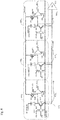
Fig. 5 shows a schematic view of two rows of reconfigurable pixels where a first row operates in a conventional SPAD output mode and a second row operates in the analogue current photodiode output mode at the same time; -
Fig. 6 shows a schematic view of a further arrangement of a row of reconfigured SPAD pixels configured to output an analogue current associated with the recharge of a SPAD diode operating in Geiger mode according to some embodiments; -
Fig. 7 shows a schematic view of a row or array of reconfigured SPAD pixels as shown inFig. 6 configured to output both analogue current and digital photon detection pulse at the same time according to some further embodiments; -
Fig. 8 shows a schematic view of a further arrangement of a row or reconfigured pixels as shown inFigure 6 but with a further modification to show the SPAD cathode is biased with voltage VPHOTOBIAS and the quench voltage is increased to a higher voltage VQUENCH_HIGH. -
Fig. 9A shows a typical voltage and current response curve of a SPAD pixel operating in Geiger mode which would be found in the reconfigured SPAD pixel as shown inFigs. 6 to 8 ; -
Fig. 9B shows a plot of quench current generated from an array of SPAD pixels as shown inFigs. 6 to 9A for an incident optical pulse of varying intensity. -
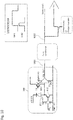
Fig. 10 shows a schematic view of a SPAD pixel with output circuitry configured to generate a controlled analogue output associated with a SPAD event from the given pixel; and -
Fig. 11 shows a schematic view showing some example configurations of how the SPAD or photodiode pixels could be configured with one or more TIA sense circuits. - The concept as embodied herein is apparatus and methods for reconfiguring a typical SPAD pixel arrangement such that it is able to produce in a further mode of operation a suitable analogue current or voltage output. The suitable analogue current or voltage output may be used to both indicate a level of illumination of the pixel in addition to providing additional TOF information.
- This reconfiguration of the SPAD pixel is useful for many different applications. For example it enables the SPAD pixel, and thus the SPAD pixel array and SPAD sensor to be used to determine not only the digital detection of single photon events which can be used for time-of-flight estimation and thus range estimation but also be used to estimate a level of illumination. This level of illumination may be used in various applications, one of which may be secure narrow beam communications between mobile devices. A secure means of communication between devices, devices and docking station, and people and their devices when they are in close proximity is important as it enables the use of a SPAD ranging module or device to transmit a modulated narrow beam of light to a further SPAD ranging module or device configured to receive the modulated narrow beam of light. The further SPAD ranging module may then demodulate and decode the data which could for example be a shared secret or cryptographic key suitable for encoding other communications and means of communications (for example via a conventional cellular or WiFi data link) between the devices.
- Thus unlike conventional RF communications, which are usually omnidirectional, by the use of narrow beams of light significantly reduce or prevent the interception and monitoring of the communications by third parties. Furthermore, the use of narrow beams of light ensures that the users of the devices know which device they are communicating with.
- Another application area in which this reconfiguration of the SPAD pixel and array can be useful is LiDAR. In a LiDAR system it is advantageous to know the number of SPAD events within a given timing window in addition to their positioning in time.
- The concept as embodied therein is therefore to use a minor modified SPAD pixel within a sensor array, where the modifications are only to the array routing or control of the pixel rather than changes to the architecture of the pixel. In implementing routing changes the embodied examples are highly compatible with existing SPAD pixel configurations.
- For example a conventional SPAD pixel configuration is shown with respect to
Fig.1 . In this sample thepixel 100 comprises adiode 151 which is reverse biased such that the diode cathode is coupled to asupply voltage 101. The supply voltage when the SPAD is operating to output a digital single photo detection event is avoltage VHV 101 which a potential higher than the reverse breakdown of the diode and allows the diode to operate in Geiger mode. Furthermorepixel 100 comprises a quenchtransistor 141 configured to be selectively operated to 'quench' the avalanche created from the single photon event. The quenchtransistor 141 is shown as an n-channel mos transistor is arranged with a drain coupled to an anode of thediode 151 and a source coupled to a 'ground'voltage supply GND 111. The quenchtransistor 141 gate is shown being controlled by the enableEN signal input 113 which switches a quenchvoltage VQUENCH 105 vialogic cell 131. - When the SPAD pixel is enabled the voltage of the
anode 151 will be close to GND assuming there are no received photons or internally generated carriers. Thus for a time the diode will be biased beyond its breakdown voltage. Upon absorption of a photon the generated electron hole pair will trigger an avalanche multiplication in the diode. This will charge theanode 151 voltage very fast until the voltage drop across the diode reduces below breakdown and the avalanche current is 'quenched'. It is noted this method of quenching the breakdown is passive quenching. Theanode 151 node voltage will then begin discharging back towards GND with the discharge current provided by the quenchtransistor 141. It is noted this method of re-arming the SPAD (biasing it beyond its breakdown voltage) is known as passive re-charging. - The
pixel 100 furthermore comprises a pull-uptransistor 161. The pull-uptransistor 161 is shown inFigure 1 as a p-channel mos transistor which is arranged such that the anode of thediode 151 is coupled to a drain of the p-channel mos transistor 161, a source of the p-channel mos transistor 161 is coupled to theoff voltage VSPADOFF 103 and a gate of the p-channel mos transistor 161 is coupled to the enableEN signal input 113. - Thus part of disabling a pixel is to reduce the voltage across the diode such that it no longer operates as a SPAD. Thus when the enable EN signal 113 is low the
anode 151 will be connected tovoltage VSPADOFF 103 which is sufficiently high to reduce the voltage across the diode below the breakdown voltage. - Furthermore the
pixel 100 comprises an output logic stage configured to detect the photon event and generate an output pulse. The output stage shown inFigure 1 is shown as a simpleCMOS logic stage 171 with asupply voltage VDDPIX 109 and a ground connection GND. Thelogic stage 171 has an input connected to thediode anode 151 and an output connected to PIX_OUT. The logic stage also has an input from the enable EN signal 113. - An individual pixel can thus be disabled so the diode no longer operates as a SPAD and the digital output is disabled. In this configuration the pixel does not create unwanted load on the VHV SPAD supply and does not contribute any output to PIX_OUT and the following circuitry.
- The concept employed herein in the following embodiments is one where a similar arrangement (or the same arrangement) to that shown in
Figure 1 is used but with different control signals to enable the pixel and the diode to output an analogue signal. The embodiments as described herein enable the pixel to operate either as a photodiode device or as a SPAD device from which able to output an analogue current or voltage which may be either in parallel with a digital event detection output with the same pixel or enable on a pixel by pixel or row by row (of pixels) basis a controllable digital photon event output or analogue illumination level output. - For example in some embodiments by controlling an array such that some of the pixels operate in a SPAD digital event detection mode and some of the pixels operate in a level intensity detection mode a sufficient signals can be generated to enable both ranging information to be determined as well as detecting and decoding an optical data stream at the same time. Furthermore in such environments it is possible to detect where the received pulses are the same as the sent pulses and to further determine whether the ranging data is contaminated by any wraparound effect.
- With respect to a first set of embodiments the diode is operated as a photodiode rather than a SPAD. For example
Figure 2 shows a modifiedpixel arrangement 200. The modified pixel arrangement differs from thepixel 100 shown inFigure 1 in the following ways. Firstly in this mode of operation the supply voltage coupled to the cathode of thediode 151 is avoltage VPHOTOBIAS 201 which (for a given anode voltage) is below the level at which the diode would operate in Geiger mode. Depending on the voltage across the diode, it may operate as a simple photodiode or an avalanche photodiode (APD). For the case of an APD, received photons have a multiplying effect to the output photocurrent but full breakdown is not achieved. - The quench
transistor 141 shown inFigure 1 in this arrangement is disabled by controlling the VQUENCH voltage to be close to (or at) the GND voltage. Furthermore the output stage is disabled by setting the enable EN signal 113 to be close to (or at) the GND voltage. In the arrangement shown inFigure 2 the pull-uptransistor 161 is furthermore used as a pass transistor. The setting of the enable EN signal 113 to be close to (or at) the GND voltage enables the pull-up to pass the current generated by thediode 151 to the VSPADOFF node as shown by therouting 251. - In the example shown in
Figure 2 the VSPADOFF node is furthermore coupled to the input of a trans-impedance amplifier (TIA) 211 input. In other embodiments the VSPADOFF node may be coupled to any suitable input amplifier. A low input impedance is required to keep the VSPADOFF node voltage constant whilst the amplification required will be dependent on the magnitude of photocurrent which will flow. - The output of the trans-
impedance amplifier 211 may then be passed or output to any suitable application. For example as shown inFigure 2 , where the illumination level detected is a received communications signal the output of the trans-impedance amplifier may be used as an input to a clock anddata recovery circuit 213 where the illumination level value is synchronised and demodulated/decoded in order to determine the received data which was optically transmitted. - It is understood that other methods of sensing current can also be applied when operating in SPAD mode and sensing current (for example such as shown later with respect to
Figure 10 ). - Furthermore the pass transistor may be an n-channel transistor with a suitable control signal rather than the p-
channel transistor 161 shown inFigure 2 . - With respect to
Figure 3 an example is shown where a row of modifiedarrangement pixels 200 are shown where the analogue current generated by each of the modifiedpixels impedance amplifier 211. In some embodiments it may be possible to selectively control the enable signal to each pixel in such a manner that individual pixels are enabled or disabled as required in order to maintain the output current to be within a defined input range for the trans-impedance amplifier 211. - It is understood that in some embodiments the modified pixels may be arranged or configured with a suitable feedback arrangement in order to attempt to cancel or allow for ambient light levels. In such embodiments the pixels may therefore output illumination level outputs which detect a change in illumination level and therefore detect communication light photons.
- For example with respect to
Figure 4A a first compensation arrangement is shown. In this example the compensation occurs external to the array wherein thepixel 200 output from the VANODE node is passed to current averager orambient level determiner 401. The current averager/ambient level determiner 401 may comprise a trans-impedance amplifier and a low pass filter arrangement which is configured to generate a 'long-term' average output current value. This 'long-term' average output current value may be passed to a controllable current-source 403 which is arranged between the VSPADOFF node and the ground supply and configured to sink a 'long-term' average output current value and thus attempt to remove the ambient component from the output of the pixel before it is detected by the amplifier. - A similar arrangement may be made by implementing a low frequency signal feedback loop to the trans-impedance amplifier.
- With respect to
Figure 4B a further compensation arrangement is shown where the compensation occurs within thepixel 200. In a manner similar to that shown in the external compensation example shown inFigure 4A the modifiedpixel 200 output from the VSPADOFF node is passed to current averager orambient level determiner 401 configured to generate the 'long-term' average output current value. However the 'long-term' average output current value in this example is passed to the gate of the quenchtransistor 141 which attempts to remove the ambient current generated from the ambient light effect on the diode by sinking the ambient current. - In some embodiments, such as shown in the example arrangement in
Figure 5 it is possible to configure an array of pixels to operate in both a SPAD single photon detection event mode and also in the analogue level of illumination mode. For example a first row ofpixels VHV 101 supply voltage and the quenchtransistor 141 is selectively operable, the pull-up transistor coupled to the VSPADOFF voltage supply (and at this point of time in the operation of the SPAD pixel disabled) and the output stage enabled in order to detect a breakdown event. - Furthermore the second row of
pixels VPHOTOBIAS 201 supply voltage, the quenchtransistor 141 is disabled, the output stage disabled and the pull-up transistor is coupled to the VSPADOFF node and thus sums theoutputs pixels impedance amplifier 211. - In the examples shown above the analogue output is provided by the pixel diode being operated in a photodiode mode. However, operation of the diode in Geiger mode can produce a current which is many times larger than current when the diode is operated as a photodiode. It should be noted that the current generated from operation in SPAD mode is not fully continuous in time as each detected event required the avalanche current to be quenched and the diode re-biased. However, in some applications such as those which use pulsed light sources, this operation is fully compatible. Thus in some embodiments the pixels may be arranged such that the current from an array of SPAD pixels are summed in order to determine information about the instantaneous illumination levels. The sensing and summing current from the SPAD pixels may be implemented, for example by reconfiguring the quench transistor such that the source is coupled to an output node. In such a way it may be possible to operate the array as an optical receiver. Thus as described previously the modified arrangement of the pixels achieve high sensitivity and furthermore are compatible with existing arrangements and architectures for standard SPAD and Time of flight detection applications.
- An example of a modified arrangement pixel 600 configured to output an analogue signal representing level of illumination when the diode is operated in Geiger mode is shown in
Figure 6 . The difference between the configuration or architecture of these modified pixels, shown as pixels 6001, 6002, and 600N inFigure 6 compared to the modifiedpixels 200 shown for example inFigure 2 is that the quenchtransistor 141 requires a separatededicated ground line 621 in order to sink the current from the photodiode caused by the diode breakdown current. - The
dedicated ground line 621 or output line for the diode and quench current caused may be input to a trans-impedance amplifier 611 or other low impedance input amplifier stage such that the trans-impedance amplifier 611 'see' the combination of currents 6511, 6512, 651N, generated from the pixels 6001, 6002, and 600N respectively. - With respect to
Figure 7 an example embodiment is shown where each modified pixel 6001, 6002, 6003, and 600N is arranged such that the pixel can output a digital output from the output stage in parallel with an analogue readout from thededicated ground line 621 or output line for the quench current caused by the SPAD breakdown by coupling the source of the quench transistors/devices to the input of the trans-impedance amplifier input. The analogue readout is biased at a low voltage and has a low impedance. - The
analogue readout line 621 can be connected by means of a switch 771 (likely a NMOS transistor) to the ground GND 111 and the pixel configuration will be the same as shown inFig.1 . - With respect to
Fig. 8 an example embodiment is shown where the diodes operate as photodiodes (biased below their breakdown voltage) and the quenchtransistor 141 is configured as a pass device. In such a configuration the quench voltage can be adjusted to reduce the resistance of the pass device. This is labelled as VQUENCH_HIGH inFig. 8 . - When considering the current summation at the trans-impedance input it is understood that the current generated by a SPAD 'event' is not a square pulse output. As mentioned previously, the quench and re-charge operations described in these embodiments is of a passive nature.
Figure 9A shows a typical profile for theanode 151 voltage and the current through the quenchdevice 141 when an event triggers the avalanche breakdown of the diode. Theanode 151 exhibits a fast charging up to a level which reduces the voltage drop across the diode to below breakdown. The increased voltage between the source and drain of the quenchtransistor 141 will cause a current to flow toGND 111 through the quench device. This current will discharge the anode back to GND. As the current flowing between drain and source of the quench transistor is dependent on the voltage, the quench current will reduce as the anode voltage drops. -
Figure 9B shows an example of how an optical pulse with different intensities can provide a similarly varying quench current. It also shows how the intensity can be sensed in a short time window.Figure 9B plots quench current from an array of SPADs over time compared with the power of the emitted optical pulse. - For the scenario where the pixel is configured to operate as a SPAD receiver it can be desirable to modify the profile of output current from that which is shown in
Fig 9A . For example, in the embodiments discussed, if the SPAD cathode voltage VHV is modified, it will have an impact on the quench current that is sensed. Similarly, if the background incident illumination is high (ambient), SPADs may not be fully re-biased before the next event is triggered. Again, this will have an impact on the quench current which is sensed. In an application where knowing the number of parallel events is important, reducing the variation of the received current per event is desirable. -
Fig. 10 shows and embodiment in which the standard digital output pulse from the SPAD pixel is used to generate an input to the TIA sense block. TheSPAD pixel output 1001 will be a digital pulse with a width relative to the quench time of the SPAD pixel. A pulse conditioner can be used to shorten the width of the digital pulse so that it is no longer relative to the re-charge time (dead time) of the SPAD pixel. The output of thepulse conditioner block 1002 can now be used to generate an input to the TIA sense circuitry which has less variability due to changes in parameters such as the VHV voltage and the SPAD dead time. The magnitude and width of the pulse provided to the TIA can also be designed independently to the SPAD pixel. - It has been mentioned that the embodiments described refer to a passive quench and re-charge of the SPAD. An alternate method of quench and re-charge well detailed in the literature is active quenching and active re-charging. These methods change the internal circuitry of a SPAD pixel (normally adding mode devices). One possible advantage is a reduction in the re-charge time by using active re-charge circuitry. This could reduce the SPAD dead time and make it available sooner to detect further incoming photons. A circuit modification to implement an active re-charge will not change the compatibility with the current sensing scheme proposed in the discussed embodiments.
- The standard readout from an array of SPAD pixels scan be done in a number of different ways. At one extreme every SPAD pixel can provide a unique digital output which can be detected in parallel. This is very possible for small array sizes but becomes more difficult as the array size increases. Routing congestion and the interface to the detection circuitry are two problems for a fully parallel readout. At the other extreme the array of SPAD pixels could have a single output with some circuitry being embedded in the array to perform the combination. A similar partitioning of the analogue readout can also be implemented if desired. Two example embodiments are shown in
Figure 11A andFigure 11B. Figure 11A shows an array of SPADs with a single analogue readout whereasFigure 11B shows a SPAD array with more than one distinct analogue output. Multiple analogue output channels may be aligned to distinct imaging areas as required by the optical design of the system or application. - In some embodiments the sensing of the current per SPAD event may be made via any other suitable supply. For example the TIA sensing circuit could be connected to the VDDPIX supply which connects to the pixel output logic stage. Similarly the GND connection of the output logic stage could be configured as the analogue output sense node. Furthermore in some embodiments the supply line VHV may be sensed to determine a current passing through the photodiode based on a SPAD event in the photodiode.
- It should be appreciated that the above described arrangements may be implemented at least partially by an integrated circuit, a chip set, one or more dies packaged together or in different packages, discrete circuitry or any combination of these options.
- Various embodiments with different variations have been described here above. It should be noted that those skilled in the art may combine various elements of these various embodiments and variations.
- Such alterations, modifications, and improvements are intended to be part of this disclosure, and are intended to be within the scope of the present invention. Accordingly, the foregoing description is by way of example only and is not intended to be limiting. The present invention is limited only as defined in the following claims and the equivalents thereto.
Claims (15)
- An apparatus comprising:at least one single photon avalanche diode pixel configured to operate in a first mode to output a digital single photon detection event, the pixel comprising:a single photon avalanche diode; andat least one output transistor configured to provide an analogue output current from the single photon avalanche diode, such that the at least one single photon avalanche diode pixel is further configured to operate in a second mode to output the analogue output current indicating a level of illumination of the pixel.
- The apparatus as claimed in claim 1, wherein the at least one single photon avalanche diode is configured to operate in the first mode and second mode at one of: different times and substantially the same time.
- The apparatus as claimed in claims 1 or 2, wherein the at least one output transistor is configured to provide the analogue output current to an input of a trans-impedance amplifier.
- The apparatus as claimed in claim 3, wherein the apparatus comprises multiple single photon avalanche diode pixels configured to provide an analogue output current from each single photon avalanche diode to the input of the trans-impedance amplifier.
- The apparatus as claimed in any of claims 1 to 4, further comprising a pulse conditioner configured to receive a single photon detection event signal pulse and control the at least one output transistor to output the analogue output current indicating a level of illumination of the pixel based on a modified length single photon detection event signal pulse.
- The apparatus as claimed in any of claims 1 to 5, further comprising a current averager to determine an average analogue output current, wherein the average analogue output current indicates an ambient level of illumination of the pixel.
- The apparatus as claimed in any of claims 1 to 6, wherein the single photon avalanche diode is configured to operate in a Geiger mode of operation in the first mode and in a photodiode mode of operation in the second mode.
- The apparatus as claimed in any of claims 1 to 7, wherein the at least one output transistor comprises at least one of:at least one quench transistor coupled to an anode of the diode and configured to drain the avalanche current following a detection event;at least one pull up transistor coupled to the anode of the diode and configured to enable the potential of the anode of the diode to be pulled up to an further supply voltage; andat least one output transistor coupled to the anode of the diode and configured to enable an output of the digital single photon detection event.
- The apparatus as claimed in claim 8, wherein when the output transistor comprises the at least one quench transistor coupled to the anode of the diode and configured to drain the avalanche current following a detection event, wherein the quench transistor is selectively enabled when the pixel is operated in the first mode.
- The apparatus as claimed in claim 9, wherein when the quench transistor is selectively enabled a quench transistor gate terminal is operated at a high voltage to reduce the impedance of the output transistor.
- The apparatus as claimed in any of claims 1 to 10, comprising at least two rows of the at least one single photon avalanche diode pixel, wherein at least one row is configured to operate in the first mode and at least one further row is configured to operate in the second row substantially at the same time.
- A method for operating a single photon avalanche diode pixel comprising a single photon avalanche diode and at least one output transistor, the method comprising:configuring the at least one single photon avalanche diode pixel to operate in a first mode to output a digital single photon detection event; andconfiguring the at least one single photon avalanche diode pixel to operate in a second mode by configuring the output transistor to provide an analogue output current from the single photon avalanche diode indicating a level of illumination of the pixel.
- The method as claimed in claim 12, wherein configuring the output transistor to provide an analogue output current from the single photon avalanche diode comprises providing to an input of a trans-impedance amplifier the analogue output current from the at least one output transistor.
- The method as claimed in claim 13, wherein providing to an input of a trans-impedance amplifier the analogue output current from the at least one output transistor comprises providing the analogue output current from multiple single photon avalanche diode pixels to the input of the trans-impedance amplifier.
- The method as claimed in any of claims 12 to 14, further comprising:modifying the pulse length of a single photon detection event signal pulse; andcontrolling the at least one output transistor to output the analogue output current indicating a level of illumination of the pixel based on the modified length single photon detection event signal pulse.
Priority Applications (2)
| Application Number | Priority Date | Filing Date | Title |
|---|---|---|---|
| EP16185753.7A EP3287813B1 (en) | 2016-08-25 | 2016-08-25 | Apparatus for detecting illumination levels |
| US15/464,563 US10641653B2 (en) | 2016-08-25 | 2017-03-21 | Apparatus for detecting illumination levels |
Applications Claiming Priority (1)
| Application Number | Priority Date | Filing Date | Title |
|---|---|---|---|
| EP16185753.7A EP3287813B1 (en) | 2016-08-25 | 2016-08-25 | Apparatus for detecting illumination levels |
Publications (2)
| Publication Number | Publication Date |
|---|---|
| EP3287813A1 true EP3287813A1 (en) | 2018-02-28 |
| EP3287813B1 EP3287813B1 (en) | 2019-10-02 |
Family
ID=56801448
Family Applications (1)
| Application Number | Title | Priority Date | Filing Date |
|---|---|---|---|
| EP16185753.7A Active EP3287813B1 (en) | 2016-08-25 | 2016-08-25 | Apparatus for detecting illumination levels |
Country Status (2)
| Country | Link |
|---|---|
| US (1) | US10641653B2 (en) |
| EP (1) | EP3287813B1 (en) |
Cited By (2)
| Publication number | Priority date | Publication date | Assignee | Title |
|---|---|---|---|---|
| WO2019176673A1 (en) * | 2018-03-16 | 2019-09-19 | Sony Semiconductor Solutions Corporation | Light receiving device and distance measuring device |
| CN111491116A (en) * | 2019-01-28 | 2020-08-04 | 原相科技股份有限公司 | Image Sensors Using Avalanche Diodes |
Families Citing this family (11)
| Publication number | Priority date | Publication date | Assignee | Title |
|---|---|---|---|---|
| US11221400B2 (en) * | 2018-03-27 | 2022-01-11 | Omnivision Technologies, Inc. | Dual mode stacked photomultipliers suitable for use in long range time of flight applications |
| EP3591712A1 (en) * | 2018-07-05 | 2020-01-08 | STMicroelectronics (Research & Development) Limited | Optical sensor and method of operating an optical sensor |
| US11579290B2 (en) * | 2019-06-05 | 2023-02-14 | Stmicroelectronics (Research & Development) Limited | LIDAR system utilizing multiple networked LIDAR integrated circuits |
| US11728621B2 (en) | 2019-06-05 | 2023-08-15 | Stmicroelectronics (Research & Development) Limited | Voltage controlled steered VCSEL driver |
| DE102019134701A1 (en) * | 2019-12-17 | 2021-06-17 | Sick Ag | Optoelectronic sensor and method for detecting an object |
| US11349042B2 (en) * | 2019-12-18 | 2022-05-31 | Stmicroelectronics (Research & Development) Limited | Anode sensing circuit for single photon avalanche diodes |
| TWI831171B (en) * | 2021-07-22 | 2024-02-01 | 神盾股份有限公司 | Optical sensing apparatus |
| CN116131833B (en) * | 2022-04-15 | 2024-06-14 | 浙桂(杭州)半导体科技有限责任公司 | Avalanche diode control circuit |
| US20230417908A1 (en) * | 2022-06-23 | 2023-12-28 | Taiwan Semiconductor Manufacturing Company Ltd. | Periodical correlation detection for background light suppression in direct time-of-flight sensor |
| FR3147429B1 (en) * | 2023-03-30 | 2025-08-15 | St Microelectronics Int Nv | Avalanche photodiode pixel |
| CN119375897A (en) * | 2023-07-25 | 2025-01-28 | 爱思开海力士有限公司 | Image sensing device for sensing distance |
Citations (4)
| Publication number | Priority date | Publication date | Assignee | Title |
|---|---|---|---|---|
| US20100214654A1 (en) * | 2007-05-22 | 2010-08-26 | Leica Microsystems Cms Gmbh | Apparatus for the detection of light in a scanning microscope |
| US20120205522A1 (en) * | 2011-02-10 | 2012-08-16 | Stmicroelectronics (Research & Development) Limited | Multi-mode photodetector |
| WO2016003451A1 (en) * | 2014-07-02 | 2016-01-07 | The Johns Hopkins University | Photodetection circuit and operating method thereof |
| US20160231168A1 (en) * | 2015-02-06 | 2016-08-11 | General Electric Company | Silicon photomultipliers with digitized micro-cells |
Family Cites Families (4)
| Publication number | Priority date | Publication date | Assignee | Title |
|---|---|---|---|---|
| US7183531B2 (en) * | 2004-03-31 | 2007-02-27 | Micron Technology, Inc. | Amplification with feedback capacitance for photodetector signals |
| JP4590974B2 (en) * | 2004-08-09 | 2010-12-01 | 住友電気工業株式会社 | Optical receiver circuit |
| EP2469301A1 (en) * | 2010-12-23 | 2012-06-27 | André Borowski | Methods and devices for generating a representation of a 3D scene at very high speed |
| US10107766B2 (en) * | 2015-01-15 | 2018-10-23 | Analogic Corporation | Photon counting imaging modes |
-
2016
- 2016-08-25 EP EP16185753.7A patent/EP3287813B1/en active Active
-
2017
- 2017-03-21 US US15/464,563 patent/US10641653B2/en active Active
Patent Citations (4)
| Publication number | Priority date | Publication date | Assignee | Title |
|---|---|---|---|---|
| US20100214654A1 (en) * | 2007-05-22 | 2010-08-26 | Leica Microsystems Cms Gmbh | Apparatus for the detection of light in a scanning microscope |
| US20120205522A1 (en) * | 2011-02-10 | 2012-08-16 | Stmicroelectronics (Research & Development) Limited | Multi-mode photodetector |
| WO2016003451A1 (en) * | 2014-07-02 | 2016-01-07 | The Johns Hopkins University | Photodetection circuit and operating method thereof |
| US20160231168A1 (en) * | 2015-02-06 | 2016-08-11 | General Electric Company | Silicon photomultipliers with digitized micro-cells |
Cited By (4)
| Publication number | Priority date | Publication date | Assignee | Title |
|---|---|---|---|---|
| WO2019176673A1 (en) * | 2018-03-16 | 2019-09-19 | Sony Semiconductor Solutions Corporation | Light receiving device and distance measuring device |
| US12204024B2 (en) | 2018-03-16 | 2025-01-21 | Sony Semiconductor Solutions Corporation | Light receiving device and distance measuring device |
| CN111491116A (en) * | 2019-01-28 | 2020-08-04 | 原相科技股份有限公司 | Image Sensors Using Avalanche Diodes |
| CN111491116B (en) * | 2019-01-28 | 2022-07-19 | 原相科技股份有限公司 | Image sensor using avalanche diode |
Also Published As
| Publication number | Publication date |
|---|---|
| US10641653B2 (en) | 2020-05-05 |
| US20180058924A1 (en) | 2018-03-01 |
| EP3287813B1 (en) | 2019-10-02 |
Similar Documents
| Publication | Publication Date | Title |
|---|---|---|
| US10641653B2 (en) | Apparatus for detecting illumination levels | |
| US11221253B2 (en) | System with a SPAD-based semiconductor device having dark pixels for monitoring sensor parameters | |
| US12085649B2 (en) | Imaging systems with single-photon avalanche diodes and ambient light level detection | |
| US11108980B2 (en) | Semiconductor devices with single-photon avalanche diode pixels | |
| US11943542B2 (en) | Imaging devices with single-photon avalanche diodes having sub-exposures for high dynamic range | |
| KR101901033B1 (en) | Spad array with pixel-level bias control | |
| CN109478553B (en) | Image sensor with large dynamic range | |
| US11913831B2 (en) | Optical sensor and method of operating an optical sensor | |
| US11846542B2 (en) | Photoelectric conversion apparatus using avalanche photodiodes with different sensitivity to light | |
| US20180033896A1 (en) | Photodetection device and photodetection system | |
| EP3936888B1 (en) | Control circuit and ranging system | |
| US20230243969A1 (en) | Sensor and distance measuring device | |
| KR20220114741A (en) | Single photon avalanche diode | |
| US11428826B2 (en) | Silicon photomultipliers with split microcells | |
| KR101381392B1 (en) | Single photon detector for reducing after pulse | |
| US20220082668A1 (en) | Light detector and distance measurement device | |
| EP3540773B1 (en) | Light detection device | |
| Li et al. | Fully-integrated SPAD-based receiver with nanosecond dead time for optical wireless communication | |
| US9000342B2 (en) | Passive type image sensor and method including first and second anti-blooming transistors discharging electric charges while integrating electric charges | |
| JP2024008923A (en) | SPAD-based devices with transistor stacks | |
| US11818488B2 (en) | Photoelectric conversion device, photoelectric conversion system, and moving body | |
| CN114551603B (en) | Avalanche photodiode | |
| US20240276123A1 (en) | Analog front end (afe) device for light-receiving sensor and method of controlling the same | |
| KR20250148741A (en) | Photon detection efficiency (pde) modulation with multi-junction single-photon avalanche diode (spad) pixels | |
| CN117826124A (en) | Logic circuit and driving method thereof, single photon laser radar |
Legal Events
| Date | Code | Title | Description |
|---|---|---|---|
| PUAI | Public reference made under article 153(3) epc to a published international application that has entered the european phase |
Free format text: ORIGINAL CODE: 0009012 |
|
| STAA | Information on the status of an ep patent application or granted ep patent |
Free format text: STATUS: THE APPLICATION HAS BEEN PUBLISHED |
|
| STAA | Information on the status of an ep patent application or granted ep patent |
Free format text: STATUS: REQUEST FOR EXAMINATION WAS MADE |
|
| AK | Designated contracting states |
Kind code of ref document: A1 Designated state(s): AL AT BE BG CH CY CZ DE DK EE ES FI FR GB GR HR HU IE IS IT LI LT LU LV MC MK MT NL NO PL PT RO RS SE SI SK SM TR |
|
| AX | Request for extension of the european patent |
Extension state: BA ME |
|
| 17P | Request for examination filed |
Effective date: 20180215 |
|
| RBV | Designated contracting states (corrected) |
Designated state(s): AL AT BE BG CH CY CZ DE DK EE ES FI FR GB GR HR HU IE IS IT LI LT LU LV MC MK MT NL NO PL PT RO RS SE SI SK SM TR |
|
| STAA | Information on the status of an ep patent application or granted ep patent |
Free format text: STATUS: EXAMINATION IS IN PROGRESS |
|
| 17Q | First examination report despatched |
Effective date: 20180716 |
|
| GRAP | Despatch of communication of intention to grant a patent |
Free format text: ORIGINAL CODE: EPIDOSNIGR1 |
|
| STAA | Information on the status of an ep patent application or granted ep patent |
Free format text: STATUS: GRANT OF PATENT IS INTENDED |
|
| INTG | Intention to grant announced |
Effective date: 20190213 |
|
| GRAS | Grant fee paid |
Free format text: ORIGINAL CODE: EPIDOSNIGR3 |
|
| GRAJ | Information related to disapproval of communication of intention to grant by the applicant or resumption of examination proceedings by the epo deleted |
Free format text: ORIGINAL CODE: EPIDOSDIGR1 |
|
| GRAL | Information related to payment of fee for publishing/printing deleted |
Free format text: ORIGINAL CODE: EPIDOSDIGR3 |
|
| STAA | Information on the status of an ep patent application or granted ep patent |
Free format text: STATUS: EXAMINATION IS IN PROGRESS |
|
| INTC | Intention to grant announced (deleted) | ||
| GRAR | Information related to intention to grant a patent recorded |
Free format text: ORIGINAL CODE: EPIDOSNIGR71 |
|
| STAA | Information on the status of an ep patent application or granted ep patent |
Free format text: STATUS: GRANT OF PATENT IS INTENDED |
|
| GRAA | (expected) grant |
Free format text: ORIGINAL CODE: 0009210 |
|
| STAA | Information on the status of an ep patent application or granted ep patent |
Free format text: STATUS: THE PATENT HAS BEEN GRANTED |
|
| INTG | Intention to grant announced |
Effective date: 20190805 |
|
| AK | Designated contracting states |
Kind code of ref document: B1 Designated state(s): AL AT BE BG CH CY CZ DE DK EE ES FI FR GB GR HR HU IE IS IT LI LT LU LV MC MK MT NL NO PL PT RO RS SE SI SK SM TR |
|
| REG | Reference to a national code |
Ref country code: GB Ref legal event code: FG4D |
|
| REG | Reference to a national code |
Ref country code: CH Ref legal event code: EP Ref country code: AT Ref legal event code: REF Ref document number: 1186821 Country of ref document: AT Kind code of ref document: T Effective date: 20191015 |
|
| REG | Reference to a national code |
Ref country code: DE Ref legal event code: R096 Ref document number: 602016021565 Country of ref document: DE |
|
| REG | Reference to a national code |
Ref country code: IE Ref legal event code: FG4D |
|
| REG | Reference to a national code |
Ref country code: NL Ref legal event code: MP Effective date: 20191002 |
|
| REG | Reference to a national code |
Ref country code: LT Ref legal event code: MG4D |
|
| REG | Reference to a national code |
Ref country code: AT Ref legal event code: MK05 Ref document number: 1186821 Country of ref document: AT Kind code of ref document: T Effective date: 20191002 |
|
| PG25 | Lapsed in a contracting state [announced via postgrant information from national office to epo] |
Ref country code: NL Free format text: LAPSE BECAUSE OF FAILURE TO SUBMIT A TRANSLATION OF THE DESCRIPTION OR TO PAY THE FEE WITHIN THE PRESCRIBED TIME-LIMIT Effective date: 20191002 Ref country code: AT Free format text: LAPSE BECAUSE OF FAILURE TO SUBMIT A TRANSLATION OF THE DESCRIPTION OR TO PAY THE FEE WITHIN THE PRESCRIBED TIME-LIMIT Effective date: 20191002 Ref country code: SE Free format text: LAPSE BECAUSE OF FAILURE TO SUBMIT A TRANSLATION OF THE DESCRIPTION OR TO PAY THE FEE WITHIN THE PRESCRIBED TIME-LIMIT Effective date: 20191002 Ref country code: PL Free format text: LAPSE BECAUSE OF FAILURE TO SUBMIT A TRANSLATION OF THE DESCRIPTION OR TO PAY THE FEE WITHIN THE PRESCRIBED TIME-LIMIT Effective date: 20191002 Ref country code: LT Free format text: LAPSE BECAUSE OF FAILURE TO SUBMIT A TRANSLATION OF THE DESCRIPTION OR TO PAY THE FEE WITHIN THE PRESCRIBED TIME-LIMIT Effective date: 20191002 Ref country code: ES Free format text: LAPSE BECAUSE OF FAILURE TO SUBMIT A TRANSLATION OF THE DESCRIPTION OR TO PAY THE FEE WITHIN THE PRESCRIBED TIME-LIMIT Effective date: 20191002 Ref country code: BG Free format text: LAPSE BECAUSE OF FAILURE TO SUBMIT A TRANSLATION OF THE DESCRIPTION OR TO PAY THE FEE WITHIN THE PRESCRIBED TIME-LIMIT Effective date: 20200102 Ref country code: GR Free format text: LAPSE BECAUSE OF FAILURE TO SUBMIT A TRANSLATION OF THE DESCRIPTION OR TO PAY THE FEE WITHIN THE PRESCRIBED TIME-LIMIT Effective date: 20200103 Ref country code: LV Free format text: LAPSE BECAUSE OF FAILURE TO SUBMIT A TRANSLATION OF THE DESCRIPTION OR TO PAY THE FEE WITHIN THE PRESCRIBED TIME-LIMIT Effective date: 20191002 Ref country code: NO Free format text: LAPSE BECAUSE OF FAILURE TO SUBMIT A TRANSLATION OF THE DESCRIPTION OR TO PAY THE FEE WITHIN THE PRESCRIBED TIME-LIMIT Effective date: 20200102 Ref country code: PT Free format text: LAPSE BECAUSE OF FAILURE TO SUBMIT A TRANSLATION OF THE DESCRIPTION OR TO PAY THE FEE WITHIN THE PRESCRIBED TIME-LIMIT Effective date: 20200203 Ref country code: FI Free format text: LAPSE BECAUSE OF FAILURE TO SUBMIT A TRANSLATION OF THE DESCRIPTION OR TO PAY THE FEE WITHIN THE PRESCRIBED TIME-LIMIT Effective date: 20191002 |
|
| PG25 | Lapsed in a contracting state [announced via postgrant information from national office to epo] |
Ref country code: RS Free format text: LAPSE BECAUSE OF FAILURE TO SUBMIT A TRANSLATION OF THE DESCRIPTION OR TO PAY THE FEE WITHIN THE PRESCRIBED TIME-LIMIT Effective date: 20191002 Ref country code: HR Free format text: LAPSE BECAUSE OF FAILURE TO SUBMIT A TRANSLATION OF THE DESCRIPTION OR TO PAY THE FEE WITHIN THE PRESCRIBED TIME-LIMIT Effective date: 20191002 Ref country code: CZ Free format text: LAPSE BECAUSE OF FAILURE TO SUBMIT A TRANSLATION OF THE DESCRIPTION OR TO PAY THE FEE WITHIN THE PRESCRIBED TIME-LIMIT Effective date: 20191002 Ref country code: IS Free format text: LAPSE BECAUSE OF FAILURE TO SUBMIT A TRANSLATION OF THE DESCRIPTION OR TO PAY THE FEE WITHIN THE PRESCRIBED TIME-LIMIT Effective date: 20200224 |
|
| PG25 | Lapsed in a contracting state [announced via postgrant information from national office to epo] |
Ref country code: AL Free format text: LAPSE BECAUSE OF FAILURE TO SUBMIT A TRANSLATION OF THE DESCRIPTION OR TO PAY THE FEE WITHIN THE PRESCRIBED TIME-LIMIT Effective date: 20191002 |
|
| REG | Reference to a national code |
Ref country code: DE Ref legal event code: R097 Ref document number: 602016021565 Country of ref document: DE |
|
| PG2D | Information on lapse in contracting state deleted |
Ref country code: IS |
|
| PG25 | Lapsed in a contracting state [announced via postgrant information from national office to epo] |
Ref country code: RO Free format text: LAPSE BECAUSE OF FAILURE TO SUBMIT A TRANSLATION OF THE DESCRIPTION OR TO PAY THE FEE WITHIN THE PRESCRIBED TIME-LIMIT Effective date: 20191002 Ref country code: DK Free format text: LAPSE BECAUSE OF FAILURE TO SUBMIT A TRANSLATION OF THE DESCRIPTION OR TO PAY THE FEE WITHIN THE PRESCRIBED TIME-LIMIT Effective date: 20191002 Ref country code: EE Free format text: LAPSE BECAUSE OF FAILURE TO SUBMIT A TRANSLATION OF THE DESCRIPTION OR TO PAY THE FEE WITHIN THE PRESCRIBED TIME-LIMIT Effective date: 20191002 Ref country code: IS Free format text: LAPSE BECAUSE OF FAILURE TO SUBMIT A TRANSLATION OF THE DESCRIPTION OR TO PAY THE FEE WITHIN THE PRESCRIBED TIME-LIMIT Effective date: 20200202 |
|
| PLBE | No opposition filed within time limit |
Free format text: ORIGINAL CODE: 0009261 |
|
| STAA | Information on the status of an ep patent application or granted ep patent |
Free format text: STATUS: NO OPPOSITION FILED WITHIN TIME LIMIT |
|
| PG25 | Lapsed in a contracting state [announced via postgrant information from national office to epo] |
Ref country code: SK Free format text: LAPSE BECAUSE OF FAILURE TO SUBMIT A TRANSLATION OF THE DESCRIPTION OR TO PAY THE FEE WITHIN THE PRESCRIBED TIME-LIMIT Effective date: 20191002 Ref country code: SM Free format text: LAPSE BECAUSE OF FAILURE TO SUBMIT A TRANSLATION OF THE DESCRIPTION OR TO PAY THE FEE WITHIN THE PRESCRIBED TIME-LIMIT Effective date: 20191002 Ref country code: IT Free format text: LAPSE BECAUSE OF FAILURE TO SUBMIT A TRANSLATION OF THE DESCRIPTION OR TO PAY THE FEE WITHIN THE PRESCRIBED TIME-LIMIT Effective date: 20191002 |
|
| 26N | No opposition filed |
Effective date: 20200703 |
|
| PG25 | Lapsed in a contracting state [announced via postgrant information from national office to epo] |
Ref country code: SI Free format text: LAPSE BECAUSE OF FAILURE TO SUBMIT A TRANSLATION OF THE DESCRIPTION OR TO PAY THE FEE WITHIN THE PRESCRIBED TIME-LIMIT Effective date: 20191002 |
|
| PG25 | Lapsed in a contracting state [announced via postgrant information from national office to epo] |
Ref country code: MC Free format text: LAPSE BECAUSE OF FAILURE TO SUBMIT A TRANSLATION OF THE DESCRIPTION OR TO PAY THE FEE WITHIN THE PRESCRIBED TIME-LIMIT Effective date: 20191002 |
|
| REG | Reference to a national code |
Ref country code: CH Ref legal event code: PL |
|
| GBPC | Gb: european patent ceased through non-payment of renewal fee |
Effective date: 20200825 |
|
| PG25 | Lapsed in a contracting state [announced via postgrant information from national office to epo] |
Ref country code: LI Free format text: LAPSE BECAUSE OF NON-PAYMENT OF DUE FEES Effective date: 20200831 Ref country code: LU Free format text: LAPSE BECAUSE OF NON-PAYMENT OF DUE FEES Effective date: 20200825 Ref country code: CH Free format text: LAPSE BECAUSE OF NON-PAYMENT OF DUE FEES Effective date: 20200831 |
|
| REG | Reference to a national code |
Ref country code: BE Ref legal event code: MM Effective date: 20200831 |
|
| PG25 | Lapsed in a contracting state [announced via postgrant information from national office to epo] |
Ref country code: FR Free format text: LAPSE BECAUSE OF NON-PAYMENT OF DUE FEES Effective date: 20200831 |
|
| PG25 | Lapsed in a contracting state [announced via postgrant information from national office to epo] |
Ref country code: BE Free format text: LAPSE BECAUSE OF NON-PAYMENT OF DUE FEES Effective date: 20200831 Ref country code: IE Free format text: LAPSE BECAUSE OF NON-PAYMENT OF DUE FEES Effective date: 20200825 Ref country code: GB Free format text: LAPSE BECAUSE OF NON-PAYMENT OF DUE FEES Effective date: 20200825 |
|
| PG25 | Lapsed in a contracting state [announced via postgrant information from national office to epo] |
Ref country code: TR Free format text: LAPSE BECAUSE OF FAILURE TO SUBMIT A TRANSLATION OF THE DESCRIPTION OR TO PAY THE FEE WITHIN THE PRESCRIBED TIME-LIMIT Effective date: 20191002 Ref country code: MT Free format text: LAPSE BECAUSE OF FAILURE TO SUBMIT A TRANSLATION OF THE DESCRIPTION OR TO PAY THE FEE WITHIN THE PRESCRIBED TIME-LIMIT Effective date: 20191002 Ref country code: CY Free format text: LAPSE BECAUSE OF FAILURE TO SUBMIT A TRANSLATION OF THE DESCRIPTION OR TO PAY THE FEE WITHIN THE PRESCRIBED TIME-LIMIT Effective date: 20191002 |
|
| PG25 | Lapsed in a contracting state [announced via postgrant information from national office to epo] |
Ref country code: MK Free format text: LAPSE BECAUSE OF FAILURE TO SUBMIT A TRANSLATION OF THE DESCRIPTION OR TO PAY THE FEE WITHIN THE PRESCRIBED TIME-LIMIT Effective date: 20191002 |
|
| PGFP | Annual fee paid to national office [announced via postgrant information from national office to epo] |
Ref country code: DE Payment date: 20250724 Year of fee payment: 10 |
|
| REG | Reference to a national code |
Ref country code: DE Ref legal event code: R082 Ref document number: 602016021565 Country of ref document: DE Representative=s name: WESTPHAL, MUSSGNUG & PARTNER PATENTANWAELTE MI, DE |