EP3285094A1 - Protective material and method for reflecting and dispersing incident energy - Google Patents
Protective material and method for reflecting and dispersing incident energy Download PDFInfo
- Publication number
- EP3285094A1 EP3285094A1 EP17179868.9A EP17179868A EP3285094A1 EP 3285094 A1 EP3285094 A1 EP 3285094A1 EP 17179868 A EP17179868 A EP 17179868A EP 3285094 A1 EP3285094 A1 EP 3285094A1
- Authority
- EP
- European Patent Office
- Prior art keywords
- dielectric mirror
- incident energy
- periodic structures
- photonic crystal
- layer
- Prior art date
- Legal status (The legal status is an assumption and is not a legal conclusion. Google has not performed a legal analysis and makes no representation as to the accuracy of the status listed.)
- Granted
Links
Images









Classifications
-
- G—PHYSICS
- G02—OPTICS
- G02B—OPTICAL ELEMENTS, SYSTEMS OR APPARATUS
- G02B5/00—Optical elements other than lenses
- G02B5/08—Mirrors
- G02B5/0816—Multilayer mirrors, i.e. having two or more reflecting layers
- G02B5/085—Multilayer mirrors, i.e. having two or more reflecting layers at least one of the reflecting layers comprising metal
- G02B5/0858—Multilayer mirrors, i.e. having two or more reflecting layers at least one of the reflecting layers comprising metal the reflecting layers comprising a single metallic layer with one or more dielectric layers
-
- G—PHYSICS
- G02—OPTICS
- G02B—OPTICAL ELEMENTS, SYSTEMS OR APPARATUS
- G02B1/00—Optical elements characterised by the material of which they are made; Optical coatings for optical elements
- G02B1/002—Optical elements characterised by the material of which they are made; Optical coatings for optical elements made of materials engineered to provide properties not available in nature, e.g. metamaterials
-
- G—PHYSICS
- G02—OPTICS
- G02B—OPTICAL ELEMENTS, SYSTEMS OR APPARATUS
- G02B1/00—Optical elements characterised by the material of which they are made; Optical coatings for optical elements
- G02B1/002—Optical elements characterised by the material of which they are made; Optical coatings for optical elements made of materials engineered to provide properties not available in nature, e.g. metamaterials
- G02B1/005—Optical elements characterised by the material of which they are made; Optical coatings for optical elements made of materials engineered to provide properties not available in nature, e.g. metamaterials made of photonic crystals or photonic band gap materials
-
- G—PHYSICS
- G02—OPTICS
- G02B—OPTICAL ELEMENTS, SYSTEMS OR APPARATUS
- G02B1/00—Optical elements characterised by the material of which they are made; Optical coatings for optical elements
- G02B1/002—Optical elements characterised by the material of which they are made; Optical coatings for optical elements made of materials engineered to provide properties not available in nature, e.g. metamaterials
- G02B1/007—Optical elements characterised by the material of which they are made; Optical coatings for optical elements made of materials engineered to provide properties not available in nature, e.g. metamaterials made of negative effective refractive index materials
-
- G—PHYSICS
- G02—OPTICS
- G02B—OPTICAL ELEMENTS, SYSTEMS OR APPARATUS
- G02B5/00—Optical elements other than lenses
- G02B5/02—Diffusing elements; Afocal elements
- G02B5/0273—Diffusing elements; Afocal elements characterized by the use
- G02B5/0284—Diffusing elements; Afocal elements characterized by the use used in reflection
-
- G—PHYSICS
- G02—OPTICS
- G02B—OPTICAL ELEMENTS, SYSTEMS OR APPARATUS
- G02B5/00—Optical elements other than lenses
- G02B5/02—Diffusing elements; Afocal elements
- G02B5/0273—Diffusing elements; Afocal elements characterized by the use
- G02B5/0294—Diffusing elements; Afocal elements characterized by the use adapted to provide an additional optical effect, e.g. anti-reflection or filter
-
- G—PHYSICS
- G02—OPTICS
- G02B—OPTICAL ELEMENTS, SYSTEMS OR APPARATUS
- G02B5/00—Optical elements other than lenses
- G02B5/08—Mirrors
- G02B5/0816—Multilayer mirrors, i.e. having two or more reflecting layers
-
- G—PHYSICS
- G02—OPTICS
- G02B—OPTICAL ELEMENTS, SYSTEMS OR APPARATUS
- G02B5/00—Optical elements other than lenses
- G02B5/08—Mirrors
- G02B5/0816—Multilayer mirrors, i.e. having two or more reflecting layers
- G02B5/0825—Multilayer mirrors, i.e. having two or more reflecting layers the reflecting layers comprising dielectric materials only
-
- G—PHYSICS
- G02—OPTICS
- G02B—OPTICAL ELEMENTS, SYSTEMS OR APPARATUS
- G02B5/00—Optical elements other than lenses
- G02B5/08—Mirrors
- G02B5/0816—Multilayer mirrors, i.e. having two or more reflecting layers
- G02B5/085—Multilayer mirrors, i.e. having two or more reflecting layers at least one of the reflecting layers comprising metal
-
- G—PHYSICS
- G02—OPTICS
- G02B—OPTICAL ELEMENTS, SYSTEMS OR APPARATUS
- G02B5/00—Optical elements other than lenses
- G02B5/20—Filters
- G02B5/28—Interference filters
- G02B5/281—Interference filters designed for the infrared light
- G02B5/282—Interference filters designed for the infrared light reflecting for infrared and transparent for visible light, e.g. heat reflectors, laser protection
-
- G—PHYSICS
- G02—OPTICS
- G02B—OPTICAL ELEMENTS, SYSTEMS OR APPARATUS
- G02B5/00—Optical elements other than lenses
- G02B5/20—Filters
- G02B5/28—Interference filters
- G02B5/285—Interference filters comprising deposited thin solid films
- G02B5/288—Interference filters comprising deposited thin solid films comprising at least one thin film resonant cavity, e.g. in bandpass filters
Definitions
- high temperature ceramic coatings Conventionally, protection of an object against incident energy, such as high energy lasers, is achieved with high temperature ceramic coatings.
- these ceramic coatings may add to the weight of the object.
- the use of high temperature ceramic coatings on objects such as aerospace vehicles may be prohibitive due to weight and/or performance requirements for the aerospace vehicle.
- high temperature ceramic coatings pose integration challenges when used on, for example, general surface materials and conformal geometries due to the brittle nature of the ceramic composites used in the high temperature ceramic coatings.
- a protective material that includes a dielectric mirror having at least one layer, each layer of the dielectric mirror being configured to reflect at least a portion of incident energy of a predetermined wavelength; and a photonic crystal array of periodic structures disposed within the dielectric mirror, the photonic crystal array of periodic structures being configured to disperse non-reflected incident energy of the predetermined wavelength transmitted through the dielectric mirror across the photonic crystal array of periodic structures in a direction parallel to a plane of the dielectric mirror.
- a protective material that includes a metallic mirror a dielectric mirror formed on the metallic mirror and having at least one layer, each layer of the dielectric mirror being configured to reflect at least a portion of incident energy of a predetermined wavelength, and a photonic crystal array of periodic structures disposed within the dielectric mirror, the photonic crystal array of periodic structures being configured to disperse non-reflected incident energy of the predetermined wavelength transmitted through the dielectric mirror across the photonic crystal array of periodic structures in a direction parallel to a plane of the dielectric mirror.
- Still another example of the subject matter according to the present disclosure relates to a method for reflecting and dispersing incident energy of a predetermined wavelength.
- the method includes reflecting at least a portion of incident energy of a predetermined wavelength with a dielectric mirror having at least one layer, each layer of the dielectric mirror reflecting a portion of the incident energy of the predetermined wavelength, and dispersing non-reflected incident energy of the predetermined wavelength transmitted through the dielectric mirror, with a photonic crystal array of periodic structures disposed within the dielectric mirror, across the photonic crystal array of periodic structures in a direction parallel to a plane of the dielectric mirror.
- the protective material 100 may be applied to a substrate 160 in any suitable manner to provide protection of the substrate 160 from incident energy, such as energy from a high energy laser.
- the substrate 160 may be an aerospace vehicle 160A, a terrestrial vehicle 160B, a maritime vessel 160C, an appliqué 160D or wearable clothing 160E (e.g. lab coats, glasses, jackets, pants, etc.).
- the protective material may be formed directly on the substrate 160 in any suitable manner such as by one or more of deposition, coating, etching, and additively forming the protective material 100 on the substrate.
- the appliqué 160D may be applied to one or more surfaces of aerospace vehicles, terrestrial vehicles, maritime vessels or to wearable clothing (e.g. such as lenses of glasses, protective body panels, etc.).
- the protective material 100 provides protection of the substrate 160 through a combination of dispersion, reflection and destructive interference of incident energy.
- the protective material 100 reflects and disperses (and scatters) the incident energy so that the incident energy is dispersed and dissipated over a larger area of the substrate and the substrate experiences little to no heating as a result of the incident energy.
- the protective material 100 includes a dielectric mirror 110 having at least one layer 111A-111n that causes destructive interference of the incident and reflected light (e.g. light that is reflected within the protective material 100).
- each layer of the dielectric mirror is configured to reflect at least a portion of incident energy of a predetermined wavelength ⁇ .
- the protective material 100 also includes one or more arrays of dielectric scatterers, such as one or more photonic crystal arrays 120 that disperse the incident energy.
- the one or more arrays of dielectric scatterers include a photonic crystal array 120 of periodic structures 130A-130n disposed within the dielectric mirror 110 where the photonic crystal array 120 of periodic structures 130A-130n is configured to disperse non-reflected incident energy of the predetermined wavelength transmitted through the dielectric mirror 110 across the photonic crystal array 120 of periodic structures 130A-130n in a direction parallel to a plane P1 of the dielectric mirror 110.
- the periodic structures 130A-130n form a Bragg reflection grating.
- each photonic crystal array 120 is coupled in direct contact to at least one of the layers 111A-111n of the dielectric mirror 110.
- Each photonic crystal array 120 includes periodic structures 130A-n, such as photonic crystals, that are in one aspect, etched into at least one layer 111A-111n of the dielectric mirror 110 while in other aspects, the periodic structures 130An are additively formed or grown on at least one layer 111A-111n of the dielectric mirror 110.
- the periodic structures 130A-n may be spatially arranged relative to one another in any suitable manner, such as in rows 190A-190n and columns 191A-191n (e.g.
- the periodic structures 130A-n may be arranged in a staggered configuration as illustrated in Fig. 1C so that the periodic structures are arranged in rows 190A-190n and offset columns 191A-191n.
- Each of the periodic structures 130A may also have any suitable shape configured to disperse and/or reflect the incident energy.
- the periodic structures may have a circular cross-section ( Figs. 1B and 1C ), a rectangular cross-section ( Fig. 1D ), a triangular cross-section (Fig.
- a polygonal (in this case hexagonal, although other polygonal shapes are possible and anticipated) cross-section Fig. IF
- a conical shape or variable cross-section Fig. 1G
- Figs. 1B-1G illustrate the periodic structures 130A in each photonic crystal array 120 array as having a common cross-section/shape (e.g. circular in Figs. 1B and 1C , rectangular in Fig. 1D , etc.) in other aspects, a single photonic crystal array 120 may have periodic structures of different shapes where, for example, a single photonic crystal array 120 may have a combination of circular, rectangular, triangular, polygonal and/or variable cross-section periodic structures 130A-n.
- the protective material includes dielectric mirror 110, photonic crystal array 120 and a metallic mirror 150 in contact with the dielectric mirror 110.
- the metallic mirror 150 is coupled to the substrate in any suitable manner such as by deposition, coating, adhesion, etc.
- the photonic crystal array 120 may be additively formed on the metallic mirror 150 or formed in a layer 111 of the dielectric mirror 110 (the layers 111 are not illustrated in Fig. 2 for clarity).
- the photonic crystal array 120 of periodic structures 130A-n is disposed between the metallic mirror 150 and an outermost surface 110S of the dielectric mirror 110.
- at least one layer 111A-111n of the dielectric mirror 110 forms a protective coating for the photonic crystal array 120 of periodic structures 130.
- the periodic structures 130A-n may be formed on or in the metallic mirror 150.
- each periodic structure 130 of the photonic crystal array 120 has an elongated body 140 having a longitudinal axis LA.
- the body 140 includes a base 140B at one longitudinal end of the body 140 and an end 140EA disposed opposite the base 140B at the other longitudinal end of the body 140.
- the periodic structure 130 is coupled to the metallic mirror 150 or a respective layer 111 at the base 140B.
- incident energy 200 such as from a high energy laser
- each layer 111A-111n of the dielectric mirror 110 reflects at least a portion of the incident energy as reflected incident energy 200RA.
- the refracted incident energy 200RF (e.g. the non-reflected incident energy) continues to travel through the dielectric mirror 110 to the photonic crystal array 120 where the periodic structures 130A at least disperse at least a portion of the refracted incident energy 200RF as dispersed refracted energy 200D.
- the periodic structures 130A-n may also reflect at least a portion of the refracted incident energy 200RF as reflected and refracted incident energy 200RP.
- the photonic crystal array 120 of periodic structures 130A-n forms a meta-material 800 (see Fig.
- the periodic structures 130A-n have a configuration and a distribution along a plane P1 of the dielectric mirror 110 (where the plane of the dielectric mirror 110 is defined by e.g. an interface surface of or between one or more layers of the dielectric mirror 110 or the outermost surface 110S of the dielectric mirror 110) so as to resonantly couple the refracted (e.g. non-reflected) incident energy 200RF and the reflected and refracted energy 200RP that is reflected by the photonic crystal array 120 of periodic structures 130A-n.
- the plane of the dielectric mirror 110 is defined by e.g. an interface surface of or between one or more layers of the dielectric mirror 110 or the outermost surface 110S of the dielectric mirror 110
- the photonic crystal array 120 of periodic structures 130A-n include band gaps that effect a negative index of refraction at an interface 260 between the dielectric mirror 110 and the periodic structures 130A-n that disperses the refracted (e.g. non-reflected) incident energy 200RF within the photonic crystal array 120 of periodic structures 130A-n by internal reflection.
- the refracted incident energy 200RF passes through the photonic crystal array 120 and is reflected by the metallic mirror 150 as reflected and refracted energy 200RB.
- the ends 140EA of the periodic structures 130A-n in Fig. 2 are illustrated as being substantially flat (e.g. in a direction substantially orthogonal to the longitudinal axis LA of the periodic structures 130A), however, in other aspects the ends of the periodic structures 130A-n may be shaped to accommodate or reflect incident energy 200 having any suitable angle of incidence 0 such as between about -45° to about +45° relative to, for example, the longitudinal axis LA of the periodic structures 130A-n (or relative to a direction substantially orthogonal to a surface of the substrate 160 where the photonic crystal array 120 is located).
- the periodic structures have nay any suitable shape to reflect incident energy 200 having an angle of incidence less than about -45° and greater than about +45° relative to, for example, the longitudinal axis LA of the periodic structures 130A-n.
- the dielectric mirror 110 includes at least one layer 111A-111n where each of the at least one layers 111A-111n has a respective thickness T1-Tn and a respective refractive index nA-nN as will be described in greater detail below.
- the at least one layer 111A-111n is a semi-transparent layer.
- the protective material 100 includes a two layer dielectric mirror 110L2 having layers 111A, 111B. It is noted that in the figures the medium 500 in which the incident energy 200 is travelling is represented for illustration purposes as a triangular shape, which is merely representative of a region in which the protective material 100 is disposed.
- the medium 500 may be the Earth's atmosphere, a liquid, a vacuum (such as e.g. space) or any other suitable medium through which the incident energy 200 is capable of traveling.
- Each layer 111A, 111B of the dielectric mirror 110 has a respective thickness T1, T2.
- the thickness T1, T2 is about one-quarter of the predetermined wavelength ⁇ of the incident energy 200 and adjusted by the respective refractive index n of the respective layer 111A, 111B.
- each layer 111 of the dielectric mirror 110 has a thickness T that is an odd multiple (1, 3, 5, 7, ...) of about one-quarter of the predetermined wavelength ⁇ adjusted by the respective refractive index n.
- the refractive index n of the layers 111 of the dielectric mirror 110 are such that the layers 111 arranged in a stack so as to have alternating high and low refractive indices n relative to adjacent layers in the stack.
- layer 111A e.g. a first layer
- the layer 111B e.g. a second layer
- the layer 111A may be a magnesium fluoride (MgF 2 ) layer having an index of refraction of about 1.37 while the layer 111B may be a gallium arsenide (GaAs) layer having an index of refraction of about 3.8.
- the layers may be made of any suitable material including but not limited to silicon dioxide (SiO 2 and tantalum pentoxide (Ta 2 O 5 ).
- the alternating high and low refractive indices n provide a dielectric mirror 110 having layers of alternating thicknesses.
- the thickness T1 of layer 111A is greater than the thickness T2 of layer 111B.
- N is the number of layers in the dielectric mirror 110
- n 0 is the refractive index of free space
- n s is the refractive index of the substrate on which the dielectric mirror 110 is disposed (which as described herein may be the metallic mirror 150 or the substrate 160 if the metallic mirror 150 is not employed).
- the layers 111 are chosen so that the dielectric mirror 110 has substantially two indices of refraction n 1 and n 2 , in other aspects the dielectric mirror may have more than two indices of refraction.
- the thickness T of each of the at least one layer 111 of the dielectric mirror 110 is such that the energy reflected (e.g. reflected incident energy 200RA and reflected and refracted energy 200RB) by each of the at least one layer 111 is in phase as illustrated in Figs. 2 and 3 .
- the two layer dielectric mirror 110L2 alone reflects about 25% of the incident energy 200 while dispersing at least a portion of the incident energy 200 (e.g. dispersed incident energy 200D) in a plane P1 of the dielectric mirror 110L2.
- the amount of incident energy reflected may be increased by adding additional layers 111 to the dielectric mirror.
- a four layer dielectric mirror 110L4 is illustrated having layers 111A-111D.
- Each of the layers 111A-111D has a respective thickness T1-T4 and a respective index of refraction n so that the indices of refraction of the layers alternates (e.g. between indices n 1 and n 2 ) and hence, the thickness T of the layers also alternates (e.g. T1 >T2 ⁇ T3>T4) as illustrated in Fig. 6A .
- the four layer dielectric mirror 110L4 reflects about 80% of the incident energy as reflected incident energy 200R (which for the purposes of Fig.
- 5B includes one or more of, e.g., reflected incident energy 200RA and reflected and refracted energy 200RB) and disperses at least a portion of the incident energy as dispersed energy 200DE which includes dispersed refracted energy 200D in the plane P1 of the dielectric mirror 110L4.
- FIG. 7A and 7B an exemplary eight layer dielectric mirror 110L8 is illustrated having layers 111A-111H.
- Each of the layers 111A-111H has a respective thickness T1-T8 and a respective index of refraction n so that the indices of refraction of the layers alternates (e.g. between indices n 1 and n 2 ) and hence, the thickness T of the layers also alternates (e.g. T1 >T2 ⁇ T3>T4 ⁇ T5>T6 ⁇ T7>T8) as illustrated in Fig. 7A .
- T1 >T2 ⁇ T3>T4 ⁇ T5>T6 ⁇ T7>T8 e.g. T1 >T2 ⁇ T3>T4 ⁇ T5>T6 ⁇ T7>T8
- the eight layer dielectric mirror 110L8 reflects about 100% of the incident energy as reflected incident energy 200R (which for the purposes of Fig. 7B includes one or more of, e.g., reflected incident energy 200RA and reflected and refracted energy 200RB) and disperses at least a portion of the incident energy as dispersed energy 200DE in the plane P1 of the dielectric mirror 110L8.
- Figs. 5B , 6B and 7B while the dielectric mirror 110 alone may reflect up to about 100% of the incident energy 200, heat is generated by the incident energy 200 in the region the incident energy impinges on the dielectric mirror 110. This heat may be transferred to the substrate 160 to which the dielectric mirror 110 is affixed.
- Figs. 5B , 6B and 7B (as well as 8B, 9B and 10) it is noted that inside the protective material 100 (inclusive of the air around the protective material) the high energy field concentration from the incident energy 200 leads to Joules heating and eventually heat generation corresponding to the areas of high energy field concentration.
- one or more photonic crystal array 120 may be provided in the dielectric mirror 110.
- photonic crystal array 120 having periodic structures 130A-n may be provided on at least one layer 111A, 111B of the two layer dielectric mirror 110L2.
- the photonic crystal array 120 is provided on layer 111A but in other aspects, the photonic crystal array may be provided on layer 111B or both layers 111 A and 111B.
- the photonic crystal array 120 provides dispersion (e.g. having a waveguide effect) of at least a portion of the incident energy 200 to the sides of the region the incident energy impinges on the dielectric mirror 110.
- the dispersed energy 200DE is dispersed across the photonic crystal array 120 of periodic structures 130A-n in a plane PC of the photonic crystal array 120 (where the plane PC of the photonic crystal array 120 is a plane that spans across the photonic crystal array 120 that is substantially parallel with an interface surface of or between one or more layers of the dielectric mirror 110 or the outermost surface 110S of the dielectric mirror 110) which in one aspect is substantially the same as the plane P1 of the dielectric mirror 110L2.
- inclusion of the photonic crystal array 120 with the dielectric mirror provides for greater dispersion of the incident energy 200 over a greater area than the dielectric mirror 110L2 alone.
- a four layer dielectric mirror 110L4 is provided having layers 111A-111D.
- a photonic crystal array 120 is provided on layer 111D so that layers 111A-111C serve as a protective coating for the photonic crystal array 120.
- the dielectric mirror is disposed on a two layer dielectric mirror 110L2 having layers 111E, 111F.
- the four layer dielectric mirror 110L4 and two layer dielectric mirror 110L2 are similar to those described above.
- the incident energy 200 is dispersed as described above with respect to Figs. 8A and 8B while also providing greater amount of reflected incident energy 200R (which for the purposes of Fig.
- 9B includes one or more of, e.g., reflected incident energy 200RA and reflected and refracted energy 200RB) than the two layer dielectric mirror 110L2 having the photonic crystal array 120.
- additional layers 111 may be added to the dielectric mirror 110 in combination with the photonic crystal array 120 so that substantially 100% of the incident energy of the predetermined wavelength ⁇ is reflected where the size and distribution of band gap features of the periodic structures 130 in the photonic crystal array 120 reflect and/or disperse substantially all of the incident energy of the predetermined wavelength ⁇ transmitted into the photonic crystal array 120 (e.g. the refracted incident energy 200RF) from the dielectric mirror 110 in the manner described above with respect to e.g. Figs. 2 and 3 .
- the metallic mirror 150 may be provided so that the metallic mirror 150 is disposed behind the photonic crystal array 120 with respect to a direction of incident energy 200 (e.g. the incident energy passes through the photonic crystal array 120 before being reflected by the metallic mirror 150).
- the protective material 100 is illustrated having a two layer dielectric mirror 110L2 with a photonic crystal array 120 disposed on layer 111 A of the dielectric mirror.
- the dielectric mirror is disposed on the metallic mirror 150.
- the incident energy 200 is reflected as reflected incident energy 200R (which for the purposes of Fig.
- reflected incident energy 200RA and reflected and refracted energy 200RB are dispersed as dispersed incident energy 200DE and scattered such that substantially no heat is generated in the region the incident energy impinges on the dielectric mirror 110.
- additional layers may be added to the dielectric mirror 110 as described above.
- the protective material 100 reflects and disperses incident energy of a predetermined wavelength.
- the protective material 100 is applied to the substrate 160 to be protected ( Fig. 11 , Block 1100).
- the dielectric mirror 110 having at least one layer 111 reflects at least a portion of incident energy 200 of a predetermined wavelength ⁇ ( Fig. 11 , Block 1110), where each layer 111 of the dielectric mirror 110 reflects a portion of the incident energy of the predetermined wavelength ⁇ .
- non-reflected incident energy e.g.
- the refracted incident energy 200RF of the predetermined wavelength ⁇ transmitted through the dielectric mirror 110 is dispersed with the photonic crystal array 120 of periodic structures 130 disposed within the dielectric mirror 110, across the photonic crystal array 120 of periodic structures 130A-130n in a direction parallel to a plane P1 of the dielectric mirror ( Fig. 11 , Block 1115).
- non-reflected incident energy (e.g. refracted incident energy 200RF) of the predetermined wavelength ⁇ transmitted through the dielectric mirror 110 is reflected with the photonic crystal array 120 of periodic structures 130A-n disposed within the dielectric mirror 110, across the photonic crystal array 120 of periodic structures 130A-n in a direction parallel to a plane P1 of the dielectric mirror ( Fig. 11 , Block 1120).
- the incident energy 200 may be reflected in phase with each of the at least one layer 111 where the thickness of each layer 111 causes the in phase reflection of the incident energy 200.
- the photonic crystal array 120 of periodic structures 130A-n may resonantly couple the non-reflected incident energy (e.g. the refracted incident energy 200RF) and reflected and refracted energy 200RP by the photonic crystal array of periodic structures.
- the non-reflected incident energy e.g. the refracted incident energy 200RF
- the non-reflected incident energy e.g. the refracted incident energy 200RF
- the non-reflected incident energy e.g. the refracted incident energy 200RF
- the refracted incident energy 200RF may be dispersed within the photonic crystal array 120 of periodic structures 130A-n by internal reflection.
- at least a portion of the non-reflected incident energy e.g. the refracted incident energy 200RF
- the metallic mirror 150 may be reflected with the metallic mirror 150 as described above.
- solid lines, if any, connecting various elements and/or components may represent mechanical, electrical, fluid, optical, electromagnetic, wireless and other couplings and/or combinations thereof.
- "coupled” means associated directly as well as indirectly.
- a member A may be directly associated with a member B, or may be indirectly associated therewith, e.g., via another member C. It will be understood that not all relationships among the various disclosed elements are necessarily represented. Accordingly, couplings other than those depicted in the drawings may also exist.
- Dashed lines, if any, connecting blocks designating the various elements and/or components represent couplings similar in function and purpose to those represented by solid lines; however, couplings represented by the dashed lines may either be selectively provided or may relate to alternative examples of the present disclosure.
- elements and/or components, if any, represented with dashed lines indicate alternative examples of the present disclosure.
- One or more elements shown in solid and/or dashed lines may be omitted from a particular example without departing from the scope of the present disclosure.
- Environmental elements, if any, are represented with dotted lines. Virtual (imaginary) elements may also be shown for clarity.
- the blocks may represent operations and/or portions thereof and lines connecting the various blocks do not imply any particular order or dependency of the operations or portions thereof. Blocks represented by dashed lines indicate alternative operations and/or portions thereof. Dashed lines, if any, connecting the various blocks represent alternative dependencies of the operations or portions thereof. It will be understood that not all dependencies among the various disclosed operations are necessarily represented.
- Fig. 11 and the accompanying disclosure describing the operations of the method(s) set forth herein should not be interpreted as necessarily determining a sequence in which the operations are to be performed. Rather, although one illustrative order is indicated, it is to be understood that the sequence of the operations may be modified when appropriate. Accordingly, certain operations may be performed in a different order or simultaneously. Additionally, those skilled in the art will appreciate that not all operations described need be performed.
- first, second, etc. are used herein merely as labels, and are not intended to impose ordinal, positional, or hierarchical requirements on the items to which these terms refer. Moreover, reference to, e.g., a “second” item does not require or preclude the existence of, e.g., a "first” or lower-numbered item, and/or, e.g., a "third" or higher-numbered item.
- a system, apparatus, structure, article, element, component, or hardware “configured to” perform a specified function is indeed capable of performing the specified function without any alteration, rather than merely having potential to perform the specified function after further modification.
- the system, apparatus, structure, article, element, component, or hardware “configured to” perform a specified function is specifically selected, created, implemented, utilized, programmed, and/or designed for the purpose of performing the specified function.
- "configured to” denotes existing characteristics of a system, apparatus, structure, article, element, component, or hardware which enable the system, apparatus, structure, article, element, component, or hardware to perform the specified function without further modification.
- a system, apparatus, structure, article, element, component, or hardware described as being “configured to” perform a particular function may additionally or alternatively be described as being “adapted to” and/or as being “operative to” perform that function.
Landscapes
- Physics & Mathematics (AREA)
- General Physics & Mathematics (AREA)
- Optics & Photonics (AREA)
- Chemical & Material Sciences (AREA)
- Crystallography & Structural Chemistry (AREA)
- Optical Elements Other Than Lenses (AREA)
Abstract
Description
- Conventionally, protection of an object against incident energy, such as high energy lasers, is achieved with high temperature ceramic coatings. However, these ceramic coatings may add to the weight of the object. In one aspect, the use of high temperature ceramic coatings on objects such as aerospace vehicles may be prohibitive due to weight and/or performance requirements for the aerospace vehicle. Further, high temperature ceramic coatings pose integration challenges when used on, for example, general surface materials and conformal geometries due to the brittle nature of the ceramic composites used in the high temperature ceramic coatings.
- Accordingly, apparatuses and methods, intended to address at least the above-identified concerns, would find utility.
- The following is a non-exhaustive list of examples, which may or may not be claimed, of the subject matter according to the present disclosure.
- One example of the subject matter according to the present disclosure relates to a protective material that includes a dielectric mirror having at least one layer, each layer of the dielectric mirror being configured to reflect at least a portion of incident energy of a predetermined wavelength; and a photonic crystal array of periodic structures disposed within the dielectric mirror, the photonic crystal array of periodic structures being configured to disperse non-reflected incident energy of the predetermined wavelength transmitted through the dielectric mirror across the photonic crystal array of periodic structures in a direction parallel to a plane of the dielectric mirror.
- Another example of the subject matter according to the present disclosure relates to a protective material that includes a metallic mirror a dielectric mirror formed on the metallic mirror and having at least one layer, each layer of the dielectric mirror being configured to reflect at least a portion of incident energy of a predetermined wavelength, and a photonic crystal array of periodic structures disposed within the dielectric mirror, the photonic crystal array of periodic structures being configured to disperse non-reflected incident energy of the predetermined wavelength transmitted through the dielectric mirror across the photonic crystal array of periodic structures in a direction parallel to a plane of the dielectric mirror.
- Still another example of the subject matter according to the present disclosure relates to a method for reflecting and dispersing incident energy of a predetermined wavelength. The method includes reflecting at least a portion of incident energy of a predetermined wavelength with a dielectric mirror having at least one layer, each layer of the dielectric mirror reflecting a portion of the incident energy of the predetermined wavelength, and dispersing non-reflected incident energy of the predetermined wavelength transmitted through the dielectric mirror, with a photonic crystal array of periodic structures disposed within the dielectric mirror, across the photonic crystal array of periodic structures in a direction parallel to a plane of the dielectric mirror.
- Having thus described examples of the present disclosure in general terms, reference will now be made to the accompanying drawings, which are not necessarily drawn to scale, and wherein like reference characters designate the same or similar parts throughout the several views, and wherein:
-
Fig. 1A is a schematic block diagram of a protective material in accordance with aspects of the present disclosure; -
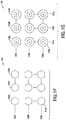
Figs. 1B-1G are schematic illustrations of partial top views of photonic crystal arrays in accordance with aspects of the present disclosure; -
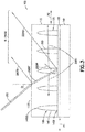
Fig. 2 is a schematic illustration of a portion of a protective material in accordance with aspects of the present disclosure; -
Fig. 3 is a schematic illustration of a portion of a protective material in accordance with aspects of the present disclosure; -
Fig. 4 is a schematic illustration of a protective material in accordance with aspects of the present disclosure; -
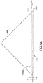
Fig. 5A is a schematic illustration of the protective material ofFig. 4 in accordance with aspects of the present disclosure; -
Fig. 5B is a schematic illustration of reflected and dispersed incident energy for the protective material illustrated inFig. 5A in accordance with aspects of the present disclosure; -
Fig. 6A is a schematic illustration of a protective material in accordance with aspects of the present disclosure; -
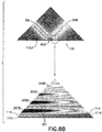
Fig. 6B is a schematic illustration of reflected and dispersed incident energy for the protective material illustrated inFig. 6A in accordance with aspects of the present disclosure; -
Fig. 7A is a schematic illustration of a protective material in accordance with aspects of the present disclosure; -
Fig. 7B is a schematic illustration of reflected and dispersed incident energy for the protective material illustrated inFig. 7A in accordance with aspects of the present disclosure; -
Fig. 8A is a schematic illustration of a protective material in accordance with aspects of the present disclosure; -
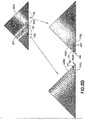
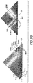
Fig. 8B is a schematic illustration of reflected and dispersed incident energy for the protective material illustrated inFig. 8A in accordance with aspects of the present disclosure; -
Fig. 9A is a schematic illustration of a protective material in accordance with aspects of the present disclosure; -
Fig. 9B is a schematic illustration of reflected and dispersed incident energy for the protective material illustrated inFig. 9A in accordance with aspects of the present disclosure; -
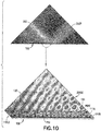
Fig. 10 is a schematic illustration of reflected and dispersed incident energy for the protective material in accordance with aspects of the present disclosure; and -
Fig. 11 is a flow diagram in accordance with aspects of the present disclosure. - Illustrative, non-exhaustive examples, which may or may not be claimed, of the subject matter according the present disclosure are provided below.
- Referring to
Fig. 1 , in accordance with the aspects of the present disclosure aprotective material 100 is provided. As will be described herein, theprotective material 100 may be applied to asubstrate 160 in any suitable manner to provide protection of thesubstrate 160 from incident energy, such as energy from a high energy laser. In one aspect thesubstrate 160 may be anaerospace vehicle 160A, aterrestrial vehicle 160B, a maritime vessel 160C, an appliqué 160D orwearable clothing 160E (e.g. lab coats, glasses, jackets, pants, etc.). In one aspect, the protective material may be formed directly on thesubstrate 160 in any suitable manner such as by one or more of deposition, coating, etching, and additively forming theprotective material 100 on the substrate. In other aspects, where theprotective material 100 is formed on an appliqué 160D the appliqué 160D may be applied to one or more surfaces of aerospace vehicles, terrestrial vehicles, maritime vessels or to wearable clothing (e.g. such as lenses of glasses, protective body panels, etc.). - In one aspect, the
protective material 100 provides protection of thesubstrate 160 through a combination of dispersion, reflection and destructive interference of incident energy. For example, theprotective material 100 reflects and disperses (and scatters) the incident energy so that the incident energy is dispersed and dissipated over a larger area of the substrate and the substrate experiences little to no heating as a result of the incident energy. In one aspect, theprotective material 100 includes adielectric mirror 110 having at least onelayer 111A-111n that causes destructive interference of the incident and reflected light (e.g. light that is reflected within the protective material 100). In one aspect, as will be described in greater detail herein, each layer of the dielectric mirror is configured to reflect at least a portion of incident energy of a predetermined wavelength λ. In one aspect, theprotective material 100 also includes one or more arrays of dielectric scatterers, such as one or morephotonic crystal arrays 120 that disperse the incident energy. As will be described in greater detail herein, the one or more arrays of dielectric scatterers include aphotonic crystal array 120 ofperiodic structures 130A-130n disposed within thedielectric mirror 110 where thephotonic crystal array 120 ofperiodic structures 130A-130n is configured to disperse non-reflected incident energy of the predetermined wavelength transmitted through thedielectric mirror 110 across thephotonic crystal array 120 ofperiodic structures 130A-130n in a direction parallel to a plane P1 of thedielectric mirror 110. In one aspect, theperiodic structures 130A-130n form a Bragg reflection grating. - Referring now to
Figs. 1A-3 , the at least onephotonic crystal array 120 is coupled in direct contact to at least one of thelayers 111A-111n of thedielectric mirror 110. Eachphotonic crystal array 120 includesperiodic structures 130A-n, such as photonic crystals, that are in one aspect, etched into at least onelayer 111A-111n of thedielectric mirror 110 while in other aspects, the periodic structures 130An are additively formed or grown on at least onelayer 111A-111n of thedielectric mirror 110. Theperiodic structures 130A-n may be spatially arranged relative to one another in any suitable manner, such as inrows 190A-190n andcolumns 191A-191n (e.g. when viewed in plan view from a top or bottom of the protective material 100) as illustrated inFigs. 1B and1D-1G . In other aspects, theperiodic structures 130A-n may be arranged in a staggered configuration as illustrated inFig. 1C so that the periodic structures are arranged inrows 190A-190n and offsetcolumns 191A-191n. Each of theperiodic structures 130A may also have any suitable shape configured to disperse and/or reflect the incident energy. For example, still referring toFigs. 1A-1G the periodic structures may have a circular cross-section (Figs. 1B and 1C ), a rectangular cross-section (Fig. 1D ), a triangular cross-section (Fig. IE), a polygonal (in this case hexagonal, although other polygonal shapes are possible and anticipated) cross-section (Fig. IF) and/or a conical shape or variable cross-section (Fig. 1G ). WhileFigs. 1B-1G illustrate theperiodic structures 130A in eachphotonic crystal array 120 array as having a common cross-section/shape (e.g. circular inFigs. 1B and 1C , rectangular inFig. 1D , etc.) in other aspects, a singlephotonic crystal array 120 may have periodic structures of different shapes where, for example, a singlephotonic crystal array 120 may have a combination of circular, rectangular, triangular, polygonal and/or variable cross-sectionperiodic structures 130A-n. - Referring to
Figs. 2 and3 an exemplaryprotective material 100 is illustrated coupled to asubstrate 160. In this aspect, the protective material includesdielectric mirror 110,photonic crystal array 120 and ametallic mirror 150 in contact with thedielectric mirror 110. Here themetallic mirror 150 is coupled to the substrate in any suitable manner such as by deposition, coating, adhesion, etc. Thephotonic crystal array 120 may be additively formed on themetallic mirror 150 or formed in a layer 111 of the dielectric mirror 110 (the layers 111 are not illustrated inFig. 2 for clarity). As can be seen inFigs. 2 and3 thephotonic crystal array 120 ofperiodic structures 130A-n is disposed between themetallic mirror 150 and anoutermost surface 110S of thedielectric mirror 110. In one aspect, at least onelayer 111A-111n of thedielectric mirror 110 forms a protective coating for thephotonic crystal array 120 ofperiodic structures 130. In one aspect, theperiodic structures 130A-n may be formed on or in themetallic mirror 150. - As can be seen in
Figs. 2 ,3 and4 eachperiodic structure 130 of thephotonic crystal array 120 has anelongated body 140 having a longitudinal axis LA. Thebody 140 includes abase 140B at one longitudinal end of thebody 140 and an end 140EA disposed opposite thebase 140B at the other longitudinal end of thebody 140. Theperiodic structure 130 is coupled to themetallic mirror 150 or a respective layer 111 at thebase 140B. As can be seen inFigs. 2 and3 , whereincident energy 200, such as from a high energy laser, is directed towards the protective material 100 (and the substrate 160) at an angle ofincidence 0, eachlayer 111A-111n of thedielectric mirror 110 reflects at least a portion of the incident energy as reflected incident energy 200RA. The refracted incident energy 200RF (e.g. the non-reflected incident energy) continues to travel through thedielectric mirror 110 to thephotonic crystal array 120 where theperiodic structures 130A at least disperse at least a portion of the refracted incident energy 200RF as dispersed refractedenergy 200D. In one aspect, theperiodic structures 130A-n may also reflect at least a portion of the refracted incident energy 200RF as reflected and refracted incident energy 200RP. In one aspect, thephotonic crystal array 120 ofperiodic structures 130A-n forms a meta-material 800 (seeFig. 8A and8B ) where theperiodic structures 130A-n have a configuration and a distribution along a plane P1 of the dielectric mirror 110 (where the plane of thedielectric mirror 110 is defined by e.g. an interface surface of or between one or more layers of thedielectric mirror 110 or theoutermost surface 110S of the dielectric mirror 110) so as to resonantly couple the refracted (e.g. non-reflected) incident energy 200RF and the reflected and refracted energy 200RP that is reflected by thephotonic crystal array 120 ofperiodic structures 130A-n. In one aspect, thephotonic crystal array 120 ofperiodic structures 130A-n include band gaps that effect a negative index of refraction at aninterface 260 between thedielectric mirror 110 and theperiodic structures 130A-n that disperses the refracted (e.g. non-reflected) incident energy 200RF within thephotonic crystal array 120 ofperiodic structures 130A-n by internal reflection. In some aspects, at least a portion of the refracted incident energy 200RF passes through thephotonic crystal array 120 and is reflected by themetallic mirror 150 as reflected and refracted energy 200RB. - The ends 140EA of the
periodic structures 130A-n inFig. 2 are illustrated as being substantially flat (e.g. in a direction substantially orthogonal to the longitudinal axis LA of theperiodic structures 130A), however, in other aspects the ends of theperiodic structures 130A-n may be shaped to accommodate or reflectincident energy 200 having any suitable angle ofincidence 0 such as between about -45° to about +45° relative to, for example, the longitudinal axis LA of theperiodic structures 130A-n (or relative to a direction substantially orthogonal to a surface of thesubstrate 160 where thephotonic crystal array 120 is located). For example, the ends of theperiodic structures 130A-n inFig. 3 are illustrated as tapered ends 140EB which accommodate or reflectincident energy 200 having a larger angle ofincidence 0 than the substantially flat ends 140EA. In other aspects, the periodic structures have nay any suitable shape to reflectincident energy 200 having an angle of incidence less than about -45° and greater than about +45° relative to, for example, the longitudinal axis LA of theperiodic structures 130A-n. - In one aspect, the
dielectric mirror 110 includes at least onelayer 111A-111n where each of the at least one layers 111A-111n has a respective thickness T1-Tn and a respective refractive index nA-nN as will be described in greater detail below. In one aspect, the at least onelayer 111A-111n is a semi-transparent layer. Referring toFigs. 4-5A , theprotective material 100 includes a two layer dielectric mirror110L2 having layers incident energy 200 is travelling is represented for illustration purposes as a triangular shape, which is merely representative of a region in which theprotective material 100 is disposed. The medium 500 may be the Earth's atmosphere, a liquid, a vacuum (such as e.g. space) or any other suitable medium through which theincident energy 200 is capable of traveling. - Each
layer dielectric mirror 110 has a respective thickness T1, T2. In one aspect, the thickness T1, T2 is about one-quarter of the predetermined wavelength λ of theincident energy 200 and adjusted by the respective refractive index n of therespective layer 
dielectric mirror 110 has a thickness T that is an odd multiple (1, 3, 5, 7, ...) of about one-quarter of the predetermined wavelength λ adjusted by the respective refractive index n. In one aspect, the refractive index n of the layers 111 of thedielectric mirror 110 are such that the layers 111 arranged in a stack so as to have alternating high and low refractive indices n relative to adjacent layers in the stack. For example, in the two layer dielectric mirror 110L2,layer 111A (e.g. a first layer) has a first refractive index n1 and thelayer 111B (e.g. a second layer) has a second refractive index n2 that is lower than the first refractive index n1 oflayer 111A. For exemplary purposes only, in one aspect, thelayer 111A may be a magnesium fluoride (MgF2) layer having an index of refraction of about 1.37 while thelayer 111B may be a gallium arsenide (GaAs) layer having an index of refraction of about 3.8. In other aspects, the layers may be made of any suitable material including but not limited to silicon dioxide (SiO2 and tantalum pentoxide (Ta2O5). The alternating high and low refractive indices n provide adielectric mirror 110 having layers of alternating thicknesses. For example, the thickness T1 oflayer 111A is greater than the thickness T2 oflayer 111B. The alternating indices of refraction n also provide thedielectric mirror 110 with a reflectance R which can be expressed as
dielectric mirror 110, n0 is the refractive index of free space and ns is the refractive index of the substrate on which thedielectric mirror 110 is disposed (which as described herein may be themetallic mirror 150 or thesubstrate 160 if themetallic mirror 150 is not employed). While in the aspects described herein the layers 111 are chosen so that thedielectric mirror 110 has substantially two indices of refraction n1 and n2, in other aspects the dielectric mirror may have more than two indices of refraction. - In one aspect, the thickness T of each of the at least one layer 111 of the
dielectric mirror 110 is such that the energy reflected (e.g. reflected incident energy 200RA and reflected and refracted energy 200RB) by each of the at least one layer 111 is in phase as illustrated inFigs. 2 and3 . - As can be seen in
Fig. 5B the two layer dielectric mirror 110L2 alone (e.g. without the photonic crystal array(s) 120 and metallic mirror 150) reflects about 25% of theincident energy 200 while dispersing at least a portion of the incident energy 200 (e.g. dispersedincident energy 200D) in a plane P1 of the dielectric mirror 110L2. The amount of incident energy reflected may be increased by adding additional layers 111 to the dielectric mirror. For example, referring now toFigs. 6A and6B a four layer dielectric mirror 110L4 is illustrated havinglayers 111A-111D. Each of thelayers 111A-111D has a respective thickness T1-T4 and a respective index of refraction n so that the indices of refraction of the layers alternates (e.g. between indices n1 and n2) and hence, the thickness T of the layers also alternates (e.g. T1 >T2<T3>T4) as illustrated inFig. 6A . As can be seen inFig. 6B , the four layer dielectric mirror 110L4 reflects about 80% of the incident energy as reflectedincident energy 200R (which for the purposes ofFig. 5B includes one or more of, e.g., reflected incident energy 200RA and reflected and refracted energy 200RB) and disperses at least a portion of the incident energy as dispersed energy 200DE which includes dispersed refractedenergy 200D in the plane P1 of the dielectric mirror 110L4. - Referring now to
Figs. 7A and7B , an exemplary eight layer dielectric mirror 110L8 is illustrated havinglayers 111A-111H. Each of thelayers 111A-111H has a respective thickness T1-T8 and a respective index of refraction n so that the indices of refraction of the layers alternates (e.g. between indices n1 and n2) and hence, the thickness T of the layers also alternates (e.g. T1 >T2<T3>T4<T5>T6<T7>T8) as illustrated inFig. 7A . As can be seen inFig. 7B , the eight layer dielectric mirror 110L8 reflects about 100% of the incident energy as reflectedincident energy 200R (which for the purposes ofFig. 7B includes one or more of, e.g., reflected incident energy 200RA and reflected and refracted energy 200RB) and disperses at least a portion of the incident energy as dispersed energy 200DE in the plane P1 of the dielectric mirror 110L8. - As can be seen in
Figs. 5B ,6B and7B , while thedielectric mirror 110 alone may reflect up to about 100% of theincident energy 200, heat is generated by theincident energy 200 in the region the incident energy impinges on thedielectric mirror 110. This heat may be transferred to thesubstrate 160 to which thedielectric mirror 110 is affixed. InFigs. 5B ,6B and7B (as well as 8B, 9B and 10) it is noted that inside the protective material 100 (inclusive of the air around the protective material) the high energy field concentration from theincident energy 200 leads to Joules heating and eventually heat generation corresponding to the areas of high energy field concentration. In the energy field plots illustrated inFigs. 5B ,6B and7B (as well as 8B, 9B and 10) it is the heat generated by theincident energy 200 that is illustrated as theincident energy 200 interacts with theprotective material 100 of the present disclosure. To reduce or substantially eliminate the amount of heat transferred to thesubstrate 160 one or morephotonic crystal array 120 may be provided in thedielectric mirror 110. For example, referring toFigs. 8A and8B , in one aspect,photonic crystal array 120 havingperiodic structures 130A-n may be provided on at least onelayer photonic crystal array 120 is provided onlayer 111A but in other aspects, the photonic crystal array may be provided onlayer 111B or bothlayers incident energy 200, thephotonic crystal array 120 provides dispersion (e.g. having a waveguide effect) of at least a portion of theincident energy 200 to the sides of the region the incident energy impinges on thedielectric mirror 110. In one aspect the dispersed energy 200DE is dispersed across thephotonic crystal array 120 ofperiodic structures 130A-n in a plane PC of the photonic crystal array 120 (where the plane PC of thephotonic crystal array 120 is a plane that spans across thephotonic crystal array 120 that is substantially parallel with an interface surface of or between one or more layers of thedielectric mirror 110 or theoutermost surface 110S of the dielectric mirror 110) which in one aspect is substantially the same as the plane P1 of the dielectric mirror 110L2. As can be seen by comparingFigs. 5B and8B , inclusion of thephotonic crystal array 120 with the dielectric mirror provides for greater dispersion of theincident energy 200 over a greater area than the dielectric mirror 110L2 alone. - Referring to
Figs. 9A and9B a four layer dielectric mirror 110L4 is provided havinglayers 111A-111D. Aphotonic crystal array 120 is provided onlayer 111D so thatlayers 111A-111C serve as a protective coating for thephotonic crystal array 120. In addition, in this aspect, the dielectric mirror is disposed on a two layer dielectric mirror110L2 having layers Fig. 9B theincident energy 200 is dispersed as described above with respect toFigs. 8A and8B while also providing greater amount of reflectedincident energy 200R (which for the purposes ofFig. 9B includes one or more of, e.g., reflected incident energy 200RA and reflected and refracted energy 200RB) than the two layer dielectric mirror 110L2 having thephotonic crystal array 120. In other aspects, additional layers 111 may be added to thedielectric mirror 110 in combination with thephotonic crystal array 120 so that substantially 100% of the incident energy of the predetermined wavelength λ is reflected where the size and distribution of band gap features of theperiodic structures 130 in thephotonic crystal array 120 reflect and/or disperse substantially all of the incident energy of the predetermined wavelength λ transmitted into the photonic crystal array 120 (e.g. the refracted incident energy 200RF) from thedielectric mirror 110 in the manner described above with respect to e.g.Figs. 2 and3 . - In one aspect, to maximize reflection, scattering and dispersion of the
incident energy 200 themetallic mirror 150 may be provided so that themetallic mirror 150 is disposed behind thephotonic crystal array 120 with respect to a direction of incident energy 200 (e.g. the incident energy passes through thephotonic crystal array 120 before being reflected by the metallic mirror 150). Referring toFig. 10 theprotective material 100 is illustrated having a two layer dielectric mirror 110L2 with aphotonic crystal array 120 disposed onlayer 111 A of the dielectric mirror. Here the dielectric mirror is disposed on themetallic mirror 150. As can be seen inFig. 10 theincident energy 200 is reflected as reflectedincident energy 200R (which for the purposes ofFig. 10 includes one or more of, e.g., reflected incident energy 200RA and reflected and refracted energy 200RB), is dispersed as dispersed incident energy 200DE and scattered such that substantially no heat is generated in the region the incident energy impinges on thedielectric mirror 110. In other aspects, to further reduce the amount of heat in the region the incident energy impinges on thedielectric mirror 110 additional layers may be added to thedielectric mirror 110 as described above. - Referring to
Figs. 1 ,2 ,3 and11 , in operation, theprotective material 100 reflects and disperses incident energy of a predetermined wavelength. As described above, theprotective material 100 is applied to thesubstrate 160 to be protected (Fig. 11 , Block 1100). Thedielectric mirror 110 having at least one layer 111 reflects at least a portion ofincident energy 200 of a predetermined wavelength λ (Fig. 11 , Block 1110), where each layer 111 of thedielectric mirror 110 reflects a portion of the incident energy of the predetermined wavelength λ. In one aspect, non-reflected incident energy (e.g. the refracted incident energy 200RF) of the predetermined wavelength λ transmitted through thedielectric mirror 110 is dispersed with thephotonic crystal array 120 ofperiodic structures 130 disposed within thedielectric mirror 110, across thephotonic crystal array 120 ofperiodic structures 130A-130n in a direction parallel to a plane P1 of the dielectric mirror (Fig. 11 , Block 1115). In one aspect, non-reflected incident energy (e.g. refracted incident energy 200RF) of the predetermined wavelength λ transmitted through thedielectric mirror 110 is reflected with thephotonic crystal array 120 ofperiodic structures 130A-n disposed within thedielectric mirror 110, across thephotonic crystal array 120 ofperiodic structures 130A-n in a direction parallel to a plane P1 of the dielectric mirror (Fig. 11 , Block 1120). In one aspect theincident energy 200 may be reflected in phase with each of the at least one layer 111 where the thickness of each layer 111 causes the in phase reflection of theincident energy 200. In one aspect, thephotonic crystal array 120 ofperiodic structures 130A-n may resonantly couple the non-reflected incident energy (e.g. the refracted incident energy 200RF) and reflected and refracted energy 200RP by the photonic crystal array of periodic structures. In one aspect, at least a portion of the non-reflected incident energy (e.g. the refracted incident energy 200RF) may be reflected with a tapered end 140EB of each of theperiodic structures 130A-n. In one aspect, the non-reflected incident energy (e.g. the refracted incident energy 200RF) may be dispersed within thephotonic crystal array 120 ofperiodic structures 130A-n by internal reflection. In one aspect, at least a portion of the non-reflected incident energy (e.g. the refracted incident energy 200RF) may be reflected with themetallic mirror 150 as described above. - The following are provided in accordance with the aspects of the present disclosure:
- A. A protective material comprising:
- a dielectric mirror having at least one layer, each layer of the dielectric mirror being configured to reflect at least a portion of incident energy of a predetermined wavelength; and
- a photonic crystal array of periodic structures disposed within the dielectric mirror, the photonic crystal array of periodic structures being configured to disperse non-reflected incident energy of the predetermined wavelength transmitted through the dielectric mirror across the photonic crystal array of periodic structures in a direction parallel to a plane of the dielectric mirror.
- A1. The protective material of paragraph A, wherein the dielectric mirror includes a first layer having a first refractive index and a second layer having a second refractive index that is lower than the first refractive index of the first layer.
- A2. The protective material of paragraph A, wherein each layer of the dielectric mirror has a thickness that is about one-quarter of the predetermined wavelength and adjusted by the respective refractive index.
- A3. The protective material of paragraph A2, wherein a thickness of each of the at least one layer is such that the incident energy reflected by each of the at least one layer is in phase.
- A4. The protective material of paragraph A, wherein each layer of the dielectric mirror has a thickness that is an odd multiple of about one-quarter of the predetermined wavelength adjusted by the respective refractive index.
- A5. The protective material of paragraph A4, wherein a thickness of each of the at least one layer is such that the incident energy reflected by each of the at least one layer is in phase.
- A6. The protective material of paragraph A, wherein the photonic crystal array of periodic structures forms a meta-material where the periodic structures have a configuration and a distribution along the plane of the dielectric mirror so as to resonantly couple the non-reflected incident energy and energy reflected by the photonic crystal array of periodic structures.
- A7. The protective material of paragraph A, wherein each of the periodic structures includes a body having base in contact with a respective layer of the dielectric mirror and a tapered end opposite the base, the tapered end being configured to reflect at least a portion of the non-reflected incident energy.
- A8. The protective material of paragraph A, wherein the photonic crystal array of periodic structures include band gaps that effect a negative index of refraction at an interface between the dielectric mirror and the periodic structures that disperses the non-reflected incident energy within the photonic crystal array of periodic structures by internal reflection.
- A9. The protective material of paragraph A, further comprising a metallic mirror in contact with the dielectric mirror, where the dielectric mirror includes an outermost surface and the photonic crystal array of periodic structures is disposed within the dielectric mirror between outermost surface and the metallic mirror.
- A10. The protective material of paragraph A, wherein at least a portion of the dielectric mirror forms a protective coating for the photonic crystal array of periodic structures.
- A11. The protective material of paragraph A, further comprising a substrate coupled to the dielectric mirror.
- A12. The protective material of paragraph A11, wherein the substrate is an appliqué.
- A13. The protective material of paragraph A11, wherein the substrate is a portion of an aerospace vehicle, a terrestrial ground vehicle or a maritime vessel.
- A14. The protective material of paragraph A11, wherein the substrate is an article of wearable clothing.
- A15. The protective material of paragraph A11, wherein the dielectric mirror is deposited as a coating on the substrate.
- A16. The protective material of paragraph A, wherein the photonic crystal array of periodic structures is etched into one layer of the dielectric mirror.
- A17. The protective material of paragraph A, wherein the photonic crystal array of periodic structures is additively formed on one layer of the dielectric mirror.
- A18. The protective material of paragraph A, wherein the at least one layer of the dielectric mirror are arranged in a stack so as to have alternating high and low refractive indices relative to adjacent layers in the stack.
- A19. The protective material of paragraph A, wherein the photonic crystal array of periodic structures forms a Bragg grating.
- B. A protective material comprising:
- a metallic mirror;
- a dielectric mirror formed on the metallic mirror and having at least one layer, each layer of the dielectric mirror being configured to reflect at least a portion of incident energy of a predetermined wavelength; and
- a photonic crystal array of periodic structures disposed within the dielectric mirror, the photonic crystal array of periodic structures being configured to disperse non-reflected incident energy of the predetermined wavelength transmitted through the dielectric mirror across the photonic crystal array of periodic structures in a direction parallel to a plane of the dielectric mirror.
- B1. The protective material of paragraph B, wherein the dielectric mirror includes a first layer having a first refractive index and a second layer having a second refractive index that is lower than the first refractive index of the first layer.
- B2. The protective material of paragraph B, wherein each layer of the dielectric mirror has a thickness that is about one-quarter of the predetermined wavelength and adjusted by the respective refractive index.
- B3. The protective material of paragraph B2, wherein a thickness of each of the at least one layer is such that the incident energy reflected by each of the at least one layer is in phase.
- B4. The protective material of paragraph B, wherein each layer of the dielectric mirror has a thickness that is an odd multiple of about one-quarter of the predetermined wavelength adjusted by the respective refractive index.
- B5. The protective material of paragraph B4, wherein a thickness of each of the at least one layer is such that the incident energy reflected by each of the at least one layer is in phase.
- B6. The protective material of paragraph B, wherein the photonic crystal array of periodic structures forms a meta-material where the periodic structures have a configuration and a distribution along the plane of the dielectric mirror so as to resonantly couple the non-reflected incident energy and energy reflected by the photonic crystal array of periodic structures.
- B7. The protective material of paragraph B, wherein each of the periodic structures includes a body having base in contact with a respective layer of the dielectric mirror and a tapered end opposite the base, the tapered end being configured to reflect at least a portion of the non-reflected incident energy.
- B8. The protective material of paragraph B, wherein the photonic crystal array of periodic structures include band gaps that effect a negative index of refraction at an interface between the dielectric mirror and the periodic structures that disperses the non-reflected incident energy within the photonic crystal array of periodic structures by internal reflection.
- B9. The protective material of paragraph B, wherein at least a portion of the dielectric mirror forms a protective coating for the photonic crystal array of periodic structures.
- B10. The protective material of paragraph B, further comprising a substrate coupled to the dielectric mirror.
- B11. The protective material of paragraph B10, wherein the substrate is an appliqué.
- B12. The protective material of paragraph B10, wherein the substrate is a portion of an aerospace vehicle, a terrestrial ground vehicle or a maritime vessel.
- B13. The protective material of paragraph B10, wherein the substrate is an article of wearable clothing.
- B14. The protective material of paragraph B10, wherein the metallic mirror is deposited as a coating on the substrate.
- B15. The protective material of paragraph B, wherein the photonic crystal array of periodic structures is etched into one layer of the dielectric mirror.
- B16. The protective material of paragraph B, wherein the photonic crystal array of periodic structures is additively formed on one layer of the dielectric mirror.
- B17. The protective material of paragraph B, wherein the at least one layer of the dielectric mirror are arranged in a stack so as to have alternating high and low refractive indices relative to adjacent layers in the stack.
- B18. The protective material of paragraph B, wherein the photonic crystal array of periodic structures forms a Bragg grating.
- C. A method for reflecting and dispersing incident energy of a predetermined wavelength, the method comprising:
- reflecting at least a portion of incident energy of a predetermined wavelength with a dielectric mirror having at least one layer, each layer of the dielectric mirror reflecting a portion of the incident energy of the predetermined wavelength; and
- dispersing non-reflected incident energy of the predetermined wavelength transmitted through the dielectric mirror, with a photonic crystal array of periodic structures disposed within the dielectric mirror, across the photonic crystal array of periodic structures in a direction parallel to a plane of the dielectric mirror.
- C1. The method of paragraph C, further comprising reflecting the incident energy in phase with each of the at least one layer.
- C2. The method of paragraph C, further comprising the resonantly coupling the non-reflected incident energy and energy reflected by the photonic crystal array of periodic structures.
- C3. The method of paragraph C, further comprising reflecting at least a portion of the non-reflected incident energy with a tapered end of each of the periodic structures.
- C4. The method of paragraph C, further comprising dispersing the non-reflected incident energy within the photonic crystal array of periodic structures by internal reflection.
- C5. The method of paragraph C, further comprising reflecting at least a portion of the non-reflected incident energy with a metallic mirror
- In the figures, referred to above, solid lines, if any, connecting various elements and/or components may represent mechanical, electrical, fluid, optical, electromagnetic, wireless and other couplings and/or combinations thereof. As used herein, "coupled" means associated directly as well as indirectly. For example, a member A may be directly associated with a member B, or may be indirectly associated therewith, e.g., via another member C. It will be understood that not all relationships among the various disclosed elements are necessarily represented. Accordingly, couplings other than those depicted in the drawings may also exist. Dashed lines, if any, connecting blocks designating the various elements and/or components represent couplings similar in function and purpose to those represented by solid lines; however, couplings represented by the dashed lines may either be selectively provided or may relate to alternative examples of the present disclosure. Likewise, elements and/or components, if any, represented with dashed lines, indicate alternative examples of the present disclosure. One or more elements shown in solid and/or dashed lines may be omitted from a particular example without departing from the scope of the present disclosure. Environmental elements, if any, are represented with dotted lines. Virtual (imaginary) elements may also be shown for clarity. Those skilled in the art will appreciate that some of the features illustrated in the figures, may be combined in various ways without the need to include other features described in the figures, other drawing figures, and/or the accompanying disclosure, even though such combination or combinations are not explicitly illustrated herein. Similarly, additional features not limited to the examples presented, may be combined with some or all of the features shown and described herein.
- In
Fig. 11 , referred to above, the blocks may represent operations and/or portions thereof and lines connecting the various blocks do not imply any particular order or dependency of the operations or portions thereof. Blocks represented by dashed lines indicate alternative operations and/or portions thereof. Dashed lines, if any, connecting the various blocks represent alternative dependencies of the operations or portions thereof. It will be understood that not all dependencies among the various disclosed operations are necessarily represented.Fig. 11 and the accompanying disclosure describing the operations of the method(s) set forth herein should not be interpreted as necessarily determining a sequence in which the operations are to be performed. Rather, although one illustrative order is indicated, it is to be understood that the sequence of the operations may be modified when appropriate. Accordingly, certain operations may be performed in a different order or simultaneously. Additionally, those skilled in the art will appreciate that not all operations described need be performed. - In the following description, numerous specific details are set forth to provide a thorough understanding of the disclosed concepts, which may be practiced without some or all of these particulars. In other instances, details of known devices and/or processes have been omitted to avoid unnecessarily obscuring the disclosure. While some concepts will be described in conjunction with specific examples, it will be understood that these examples are not intended to be limiting.
- Unless otherwise indicated, the terms "first," "second," etc. are used herein merely as labels, and are not intended to impose ordinal, positional, or hierarchical requirements on the items to which these terms refer. Moreover, reference to, e.g., a "second" item does not require or preclude the existence of, e.g., a "first" or lower-numbered item, and/or, e.g., a "third" or higher-numbered item.
- Reference herein to "one example" means that one or more feature, structure, or characteristic described in connection with the example is included in at least one implementation. The phrase "one example" in various places in the specification may or may not be referring to the same example.
- As used herein, a system, apparatus, structure, article, element, component, or hardware "configured to" perform a specified function is indeed capable of performing the specified function without any alteration, rather than merely having potential to perform the specified function after further modification. In other words, the system, apparatus, structure, article, element, component, or hardware "configured to" perform a specified function is specifically selected, created, implemented, utilized, programmed, and/or designed for the purpose of performing the specified function. As used herein, "configured to" denotes existing characteristics of a system, apparatus, structure, article, element, component, or hardware which enable the system, apparatus, structure, article, element, component, or hardware to perform the specified function without further modification. For purposes of this disclosure, a system, apparatus, structure, article, element, component, or hardware described as being "configured to" perform a particular function may additionally or alternatively be described as being "adapted to" and/or as being "operative to" perform that function.
- Different examples of the apparatus(es) and method(s) disclosed herein include a variety of components, features, and functionalities. It should be understood that the various examples of the apparatus(es) and method(s) disclosed herein may include any of the components, features, and functionalities of any of the other examples of the apparatus(es) and method(s) disclosed herein in any combination, and all of such possibilities are intended to be within the scope of the present disclosure.
- Further, the disclosure comprises embodiments according to the following clauses:
- Clause 1. A protective material comprising:
- a dielectric mirror having at least one layer, each layer of the dielectric mirror being configured to reflect at least a portion of incident energy of a predetermined wavelength; and
- a photonic crystal array of periodic structures disposed within the dielectric mirror, the photonic crystal array of periodic structures being configured to disperse non-reflected incident energy of the predetermined wavelength transmitted through the dielectric mirror across the photonic crystal array of periodic structures in a direction parallel to a plane of the dielectric mirror.
- Clause 2. The protective material of Clause 1, wherein the dielectric mirror includes a first layer having a first refractive index and a second layer having a second refractive index that is lower than the first refractive index of the first layer.
- Clause 3. The protective material of any of Clauses 1-2, wherein each layer of the dielectric mirror has a thickness that is about one-quarter of the predetermined wavelength and adjusted by the respective refractive index.
- Clause 4. The protective material of any of Clauses 1-3, wherein the photonic crystal array of periodic structures forms a meta-material where the periodic structures have a configuration and a distribution along the plane of the dielectric mirror so as to resonantly couple the non-reflected incident energy and energy reflected by the photonic crystal array of periodic structures.
- Clause 5. The protective material of any of Clauses 1-4, wherein each of the periodic structures includes a body having base in contact with a respective layer of the dielectric mirror and a tapered end opposite the base, the tapered end being configured to reflect at least a portion of the non-reflected incident energy.
- Clause 6. The protective material of any of Clauses 1-5, wherein the photonic crystal array of periodic structures include band gaps that effect a negative index of refraction at an interface between the dielectric mirror and the periodic structures that disperses the non-reflected incident energy within the photonic crystal array of periodic structures by internal reflection.
- Clause 7. The protective material of any of Clauses 1-6, further comprising a metallic mirror in contact with the dielectric mirror, where the dielectric mirror includes an outermost surface and the photonic crystal array of periodic structures is disposed within the dielectric mirror between outermost surface and the metallic mirror.
- Clause 8. The protective material of any of Clauses 1-7, wherein at least a portion of the dielectric mirror forms a protective coating for the photonic crystal array of periodic structures.
- Clause 9. The protective material of any of Clauses 1-8, further comprising a substrate coupled to the dielectric mirror.
- Clause 10. The protective material of any of Clauses 1-9, wherein the at least one layer of the dielectric mirror are arranged in a stack so as to have alternating high and low refractive indices relative to adjacent layers in the stack.
- Clause 11. A protective material comprising:
- a metallic mirror;
- a dielectric mirror formed on the metallic mirror and having at least one layer, each layer of the dielectric mirror being configured to reflect at least a portion of incident energy of a predetermined wavelength; and
- a photonic crystal array of periodic structures disposed within the dielectric mirror, the photonic crystal array of periodic structures being configured to disperse non-reflected incident energy of the predetermined wavelength transmitted through the dielectric mirror across the photonic crystal array of periodic structures in a direction parallel to a plane of the dielectric mirror.
- Clause 12. The protective material of Clause 11, wherein the dielectric mirror includes a first layer having a first refractive index and a second layer having a second refractive index that is lower than the first refractive index of the first layer.
- Clause 13. The protective material of any of Clauses 11-12, wherein each layer of the dielectric mirror has a thickness that is about one-quarter of the predetermined wavelength and adjusted by the respective refractive index.
- Clause 14. The protective material of any of Clauses 11-13, wherein the photonic crystal array of periodic structures include band gaps that effect a negative index of refraction at an interface between the dielectric mirror and the periodic structures that disperses the non-reflected incident energy within the photonic crystal array of periodic structures by internal reflection.
-
Clause 15. A method for reflecting and dispersing incident energy of a predetermined wavelength, the method comprising:- reflecting at least a portion of incident energy of a predetermined wavelength with a dielectric mirror having at least one layer, each layer of the dielectric mirror reflecting a portion of the incident energy of the predetermined wavelength; and
- dispersing non-reflected incident energy of the predetermined wavelength transmitted through the dielectric mirror, with a photonic crystal array of periodic structures disposed within the dielectric mirror, across the photonic crystal array of periodic structures in a direction parallel to a plane of the dielectric mirror.
- Clause 16. The method of
Clause 15, further comprising reflecting the incident energy in phase with each of the at least one layer. -
Clause 17. The method of any of Clauses 15-16, further comprising the resonantly coupling the non-reflected incident energy and energy reflected by the photonic crystal array of periodic structures. - Clause 18. The method of any of Clauses 15-17, further comprising reflecting at least a portion of the non-reflected incident energy with a tapered end of each of the periodic structures.
- Clause 19. The method of any of Clauses 15-18, further comprising dispersing the non-reflected incident energy within the photonic crystal array of periodic structures by internal reflection.
- Clause 20. The method of any of Clauses 15-19, further comprising reflecting at least a portion of the non-reflected incident energy with a metallic mirror.
- Many modifications of examples set forth herein will come to mind to one skilled in the art to which the present disclosure pertains having the benefit of the teachings presented in the foregoing descriptions and the associated drawings.
- Therefore, it is to be understood that the present disclosure is not to be limited to the specific examples illustrated and that modifications and other examples are intended to be included within the scope of the appended claims. Moreover, although the foregoing description and the associated drawings describe examples of the present disclosure in the context of certain illustrative combinations of elements and/or functions, it should be appreciated that different combinations of elements and/or functions may be provided by alternative implementations without departing from the scope of the appended claims. Accordingly, parenthetical reference numerals in the appended claims are presented for illustrative purposes only and are not intended to limit the scope of the claimed subject matter to the specific examples provided in the present disclosure.
Claims (15)
- A protective material (100) comprising:a dielectric mirror (110) having at least one layer (111), each layer (111A-111n) of the dielectric mirror (110) being configured to reflect at least a portion of incident energy (200) of a predetermined wavelength; anda photonic crystal array (120) of periodic structures (130A-130n) disposed within the dielectric mirror (110), the photonic crystal array (120) of periodic structures (130A-130n) being configured to disperse non-reflected incident energy (200RF) of the predetermined wavelength transmitted through the dielectric mirror (110) across the photonic crystal array (120) of periodic structures (130A-130n) in a direction parallel to a plane (P1) of the dielectric mirror (110).
- The protective material (100) of claim 1, wherein the dielectric mirror (110) includes a first layer (111 A-111n) having a first refractive index (nA-nN) and a second layer (111A-111n) having a second refractive index (nA-nN) that is lower than the first refractive index (nA-nN) of the first layer (111A-111n).
- The protective material (100) of any of claims 1-2, wherein each layer (111A-111n) of the dielectric mirror (110) has a thickness (T) that is about one-quarter of the predetermined wavelength and adjusted by the respective refractive index (nA-nN).
- The protective material (100) of any of claims 1-3, wherein the photonic crystal array (120) of periodic structures (130A-130n) forms a meta-material (800) where the periodic structures (130A-130n) have a configuration and a distribution along the plane (P1) of the dielectric mirror (110) so as to resonantly couple the non-reflected incident energy (200RF) and energy reflected (200RA) by the photonic crystal array (120) of periodic structures (130A-130n).
- The protective material (100) of any of claims 1-4, wherein each of the periodic structures (130A-130n) includes a body (140) having base (140B) in contact with a respective layer (111A-111n) of the dielectric mirror (110) and a tapered end (140EB) opposite the base (140B), the tapered end (140EB) being configured to reflect at least a portion of the non-reflected incident energy (200RF).
- The protective material (100) of any of claims 1-5, wherein the photonic crystal array (120) of periodic structures (130A-130n) include band gaps that effect a negative index of refraction at an interface (260) between the dielectric mirror (110) and the periodic structures (130A-130n) that disperses the non-reflected incident energy (200RF) within the photonic crystal array (120) of periodic structures (130A-130n) by internal reflection.
- The protective material (100) of any of claims 1-6, further comprising a metallic mirror (150) in contact with the dielectric mirror (110), where the dielectric mirror (110) includes an outermost surface and the photonic crystal array (120) of periodic structures (130A-130n) is disposed within the dielectric mirror (110) between outermost surface (110S) and the metallic mirror (150).
- The protective material (100) of any of claims 1-7, wherein at least a portion of the dielectric mirror (110) forms a protective coating for the photonic crystal array (120) of periodic structures (130A-130n).
- The protective material (100) of any of claims 1-8, further comprising a substrate (160) coupled to the dielectric mirror (110).
- The protective material (100) of any of claims 1-9, wherein the at least one layer of the dielectric mirror (110) are arranged in a stack so as to have alternating high and low refractive indices relative to adjacent layers (111A-111n) in the stack.
- A method for reflecting and dispersing incident energy (200) of a predetermined wavelength, the method comprising:reflecting at least a portion of incident energy (200) of a predetermined wavelength with a dielectric mirror (110) having at least one layer (111), each layer (111A-111n) of the dielectric mirror (110) reflecting a portion of the incident energy (200) of the predetermined wavelength; anddispersing non-reflected incident energy (200RF) of the predetermined wavelength transmitted through the dielectric mirror (110), with a photonic crystal array (120) of periodic structures (130A-130n) disposed within the dielectric mirror (110), across the photonic crystal array (120) of periodic structures (130A-130n) in a direction parallel to a plane (P1) of the dielectric mirror (110).
- The method of claim 11, further comprising reflecting the incident energy (200) in phase with each of the at least one layer (111A-111n).
- The method of any of claims 11-12, further comprising the resonantly coupling the non-reflected incident energy (200RF) and energy reflected (200RA) by the photonic crystal array (120) of periodic structures (130A-130n).
- The method of any of claims 11-13, further comprising reflecting at least a portion of the non-reflected incident energy (200RF) with a tapered end (140EB) of each of the periodic structures (130A-130n).
- The method of any of claims 11-14, further comprising dispersing the non-reflected incident energy (200RF) within the photonic crystal array (120) of periodic structures (130A-130n) by internal reflection and, optionally, further comprising reflecting at least a portion of the non-reflected incident energy (200RF) with a metallic mirror (150).
Applications Claiming Priority (1)
| Application Number | Priority Date | Filing Date | Title |
|---|---|---|---|
| US15/239,925 US10126471B2 (en) | 2016-08-18 | 2016-08-18 | Protective material and method for reflecting and dispersing incident energy |
Publications (2)
| Publication Number | Publication Date |
|---|---|
| EP3285094A1 true EP3285094A1 (en) | 2018-02-21 |
| EP3285094B1 EP3285094B1 (en) | 2022-04-27 |
Family
ID=59362921
Family Applications (1)
| Application Number | Title | Priority Date | Filing Date |
|---|---|---|---|
| EP17179868.9A Active EP3285094B1 (en) | 2016-08-18 | 2017-07-05 | Protective material and method for reflecting and dispersing incident energy |
Country Status (2)
| Country | Link |
|---|---|
| US (1) | US10126471B2 (en) |
| EP (1) | EP3285094B1 (en) |
Citations (3)
| Publication number | Priority date | Publication date | Assignee | Title |
|---|---|---|---|---|
| US4281894A (en) * | 1980-01-21 | 1981-08-04 | The Perkin-Elmer Corporation | Very low absorption, low efficiency laser beamsampler |
| US5907436A (en) * | 1995-09-29 | 1999-05-25 | The Regents Of The University Of California | Multilayer dielectric diffraction gratings |
| US7903338B1 (en) * | 2006-07-08 | 2011-03-08 | Cirrex Systems Llc | Method and system for managing light at an optical interface |
Family Cites Families (4)
| Publication number | Priority date | Publication date | Assignee | Title |
|---|---|---|---|---|
| MXPA04008400A (en) * | 2002-02-28 | 2004-11-26 | Solutia Inc | Embossed reflective laminates. |
| KR101466831B1 (en) * | 2013-07-03 | 2014-11-28 | 코닝정밀소재 주식회사 | Light extraction substrate for oled, method of fabricating thereof and oled including the same |
| CN103409801B (en) * | 2013-08-13 | 2016-06-08 | 厦门大学 | A kind of preparation method of high intensity crosslinking polymer crystal film with photon |
| WO2015112918A1 (en) * | 2014-01-24 | 2015-07-30 | General Plasma, Inc. | Scratch and fingerprint resistant anti-reflective films for use on display windows of electronic devices and other related technology |
-
2016
- 2016-08-18 US US15/239,925 patent/US10126471B2/en active Active
-
2017
- 2017-07-05 EP EP17179868.9A patent/EP3285094B1/en active Active
Patent Citations (3)
| Publication number | Priority date | Publication date | Assignee | Title |
|---|---|---|---|---|
| US4281894A (en) * | 1980-01-21 | 1981-08-04 | The Perkin-Elmer Corporation | Very low absorption, low efficiency laser beamsampler |
| US5907436A (en) * | 1995-09-29 | 1999-05-25 | The Regents Of The University Of California | Multilayer dielectric diffraction gratings |
| US7903338B1 (en) * | 2006-07-08 | 2011-03-08 | Cirrex Systems Llc | Method and system for managing light at an optical interface |
Non-Patent Citations (1)
| Title |
|---|
| JINLONG HE ET AL: "Slow light in a dielectric waveguide with negative-refractive-index photonic crystal cladding", OPTICS EXPRESS, 21 July 2008 (2008-07-21), United States, pages 11077 - 11082, XP055440248, Retrieved from the Internet <URL:https://www.osapublishing.org/DirectPDFAccess/FE6870CB-ADA7-4515-493FB9C7A25F6C13_167311/oe-16-15-11077.pdf?da=1&id=167311&seq=0&mobile=no> [retrieved on 20180111], DOI: 10.1364/OE.16.011077 * |
Also Published As
| Publication number | Publication date |
|---|---|
| EP3285094B1 (en) | 2022-04-27 |
| US20180052261A1 (en) | 2018-02-22 |
| US10126471B2 (en) | 2018-11-13 |
Similar Documents
| Publication | Publication Date | Title |
|---|---|---|
| US5151956A (en) | Waveguide polarizer using localized surface plasmons | |
| Maaroof et al. | Mie and Bragg plasmons in subwavelength silver semi‐shells | |
| Robbiano et al. | Hybrid plasmonic–photonic nanostructures: gold nanocrescents over opals | |
| Rockstuhl et al. | Optical activity in chiral media composed of three-dimensional metallic meta-atoms | |
| Srivastava et al. | Enhancement of omnidirectional reflection in photonic crystal heterostructures | |
| WO2010000542A1 (en) | Diffractive polarizing mirror device | |
| Barkat | Theoretical investigation of transmission and dispersion properties of one dimensional photonic crystal | |
| Prokhorov et al. | Quasitrapped modes in metasurfaces of anisotropic MoS 2 nanoparticles for absorption and polarization control in the telecom wavelength range | |
| Wu et al. | Analysis of optical reflection in a chirped distributed Bragg reflector | |
| Khomeriki et al. | Photonic ferroelectric vortex lattice | |
| Fradkin et al. | Thickness-independent narrow resonance in a stack of plasmonic lattices | |
| EP3285094A1 (en) | Protective material and method for reflecting and dispersing incident energy | |
| Kats et al. | Polarization properties of a periodically-modulated metal film in regions of anomalous optical transparency | |
| Gharaati et al. | Characterization of defect modes in onedimensional ternary metallo-dielectric nanolayered photonic crystal | |
| Del Barco et al. | Omnidirectional high-reflectivity mirror in the 4–20 μ m spectral range | |
| Li et al. | High reflectivity design of the one-dimensional heterostructure photonic crystal in 3 to 5 and 8 to 12 μ m infrared regions | |
| Fehrembach et al. | Filtering of unpolarized light by gratings | |
| Behera et al. | Polarization dependent enhanced infrared transmission through complementary nanostructured gold films | |
| Avrutsky et al. | Resonant diffraction into symmetry-prohibited orders of metal gratings | |
| Morozov et al. | High-order bandgaps in one-dimensional photonic crystals | |
| Mouldi et al. | Numerical Study of the Dielectric Omnidirectional Visible Mirror | |
| Laroche et al. | Polarization conversion with a photonic crystal slab | |
| Mujeeb et al. | Effect of orientation on excitation of surface-plasmon-polariton waves guided by a columnar thin film deposited on a metal grating (Erratum) | |
| Rubio et al. | Geometric frustration in ordered lattices of plasmonic nanoelements | |
| Zipp et al. | High reflectivity metamaterial of close-packed dielectric spheres |
Legal Events
| Date | Code | Title | Description |
|---|---|---|---|
| PUAI | Public reference made under article 153(3) epc to a published international application that has entered the european phase |
Free format text: ORIGINAL CODE: 0009012 |
|
| STAA | Information on the status of an ep patent application or granted ep patent |
Free format text: STATUS: REQUEST FOR EXAMINATION WAS MADE |
|
| 17P | Request for examination filed |
Effective date: 20170705 |
|
| AK | Designated contracting states |
Kind code of ref document: A1 Designated state(s): AL AT BE BG CH CY CZ DE DK EE ES FI FR GB GR HR HU IE IS IT LI LT LU LV MC MK MT NL NO PL PT RO RS SE SI SK SM TR |
|
| AX | Request for extension of the european patent |
Extension state: BA ME |
|
| GRAP | Despatch of communication of intention to grant a patent |
Free format text: ORIGINAL CODE: EPIDOSNIGR1 |
|
| STAA | Information on the status of an ep patent application or granted ep patent |
Free format text: STATUS: GRANT OF PATENT IS INTENDED |
|
| RIC1 | Information provided on ipc code assigned before grant |
Ipc: G02B 5/28 20060101ALI20211020BHEP Ipc: G02B 5/08 20060101ALI20211020BHEP Ipc: G02B 5/02 20060101ALI20211020BHEP Ipc: G02B 1/00 20060101AFI20211020BHEP |
|
| INTG | Intention to grant announced |
Effective date: 20211110 |
|
| GRAS | Grant fee paid |
Free format text: ORIGINAL CODE: EPIDOSNIGR3 |
|
| GRAA | (expected) grant |
Free format text: ORIGINAL CODE: 0009210 |
|
| STAA | Information on the status of an ep patent application or granted ep patent |
Free format text: STATUS: THE PATENT HAS BEEN GRANTED |
|
| AK | Designated contracting states |
Kind code of ref document: B1 Designated state(s): AL AT BE BG CH CY CZ DE DK EE ES FI FR GB GR HR HU IE IS IT LI LT LU LV MC MK MT NL NO PL PT RO RS SE SI SK SM TR |
|
| REG | Reference to a national code |
Ref country code: GB Ref legal event code: FG4D |
|
| REG | Reference to a national code |
Ref country code: CH Ref legal event code: EP |
|
| REG | Reference to a national code |
Ref country code: DE Ref legal event code: R096 Ref document number: 602017056458 Country of ref document: DE |
|
| REG | Reference to a national code |
Ref country code: AT Ref legal event code: REF Ref document number: 1487365 Country of ref document: AT Kind code of ref document: T Effective date: 20220515 |
|
| REG | Reference to a national code |
Ref country code: IE Ref legal event code: FG4D |
|
| REG | Reference to a national code |
Ref country code: LT Ref legal event code: MG9D |
|
| REG | Reference to a national code |
Ref country code: NL Ref legal event code: MP Effective date: 20220427 |
|
| REG | Reference to a national code |
Ref country code: AT Ref legal event code: MK05 Ref document number: 1487365 Country of ref document: AT Kind code of ref document: T Effective date: 20220427 |
|
| PG25 | Lapsed in a contracting state [announced via postgrant information from national office to epo] |
Ref country code: NL Free format text: LAPSE BECAUSE OF FAILURE TO SUBMIT A TRANSLATION OF THE DESCRIPTION OR TO PAY THE FEE WITHIN THE PRESCRIBED TIME-LIMIT Effective date: 20220427 |
|
| PG25 | Lapsed in a contracting state [announced via postgrant information from national office to epo] |
Ref country code: SE Free format text: LAPSE BECAUSE OF FAILURE TO SUBMIT A TRANSLATION OF THE DESCRIPTION OR TO PAY THE FEE WITHIN THE PRESCRIBED TIME-LIMIT Effective date: 20220427 Ref country code: PT Free format text: LAPSE BECAUSE OF FAILURE TO SUBMIT A TRANSLATION OF THE DESCRIPTION OR TO PAY THE FEE WITHIN THE PRESCRIBED TIME-LIMIT Effective date: 20220829 Ref country code: NO Free format text: LAPSE BECAUSE OF FAILURE TO SUBMIT A TRANSLATION OF THE DESCRIPTION OR TO PAY THE FEE WITHIN THE PRESCRIBED TIME-LIMIT Effective date: 20220727 Ref country code: LT Free format text: LAPSE BECAUSE OF FAILURE TO SUBMIT A TRANSLATION OF THE DESCRIPTION OR TO PAY THE FEE WITHIN THE PRESCRIBED TIME-LIMIT Effective date: 20220427 Ref country code: HR Free format text: LAPSE BECAUSE OF FAILURE TO SUBMIT A TRANSLATION OF THE DESCRIPTION OR TO PAY THE FEE WITHIN THE PRESCRIBED TIME-LIMIT Effective date: 20220427 Ref country code: GR Free format text: LAPSE BECAUSE OF FAILURE TO SUBMIT A TRANSLATION OF THE DESCRIPTION OR TO PAY THE FEE WITHIN THE PRESCRIBED TIME-LIMIT Effective date: 20220728 Ref country code: FI Free format text: LAPSE BECAUSE OF FAILURE TO SUBMIT A TRANSLATION OF THE DESCRIPTION OR TO PAY THE FEE WITHIN THE PRESCRIBED TIME-LIMIT Effective date: 20220427 Ref country code: ES Free format text: LAPSE BECAUSE OF FAILURE TO SUBMIT A TRANSLATION OF THE DESCRIPTION OR TO PAY THE FEE WITHIN THE PRESCRIBED TIME-LIMIT Effective date: 20220427 Ref country code: BG Free format text: LAPSE BECAUSE OF FAILURE TO SUBMIT A TRANSLATION OF THE DESCRIPTION OR TO PAY THE FEE WITHIN THE PRESCRIBED TIME-LIMIT Effective date: 20220727 Ref country code: AT Free format text: LAPSE BECAUSE OF FAILURE TO SUBMIT A TRANSLATION OF THE DESCRIPTION OR TO PAY THE FEE WITHIN THE PRESCRIBED TIME-LIMIT Effective date: 20220427 |
|
| PG25 | Lapsed in a contracting state [announced via postgrant information from national office to epo] |
Ref country code: RS Free format text: LAPSE BECAUSE OF FAILURE TO SUBMIT A TRANSLATION OF THE DESCRIPTION OR TO PAY THE FEE WITHIN THE PRESCRIBED TIME-LIMIT Effective date: 20220427 Ref country code: PL Free format text: LAPSE BECAUSE OF FAILURE TO SUBMIT A TRANSLATION OF THE DESCRIPTION OR TO PAY THE FEE WITHIN THE PRESCRIBED TIME-LIMIT Effective date: 20220427 Ref country code: LV Free format text: LAPSE BECAUSE OF FAILURE TO SUBMIT A TRANSLATION OF THE DESCRIPTION OR TO PAY THE FEE WITHIN THE PRESCRIBED TIME-LIMIT Effective date: 20220427 Ref country code: IS Free format text: LAPSE BECAUSE OF FAILURE TO SUBMIT A TRANSLATION OF THE DESCRIPTION OR TO PAY THE FEE WITHIN THE PRESCRIBED TIME-LIMIT Effective date: 20220827 |
|
| REG | Reference to a national code |
Ref country code: DE Ref legal event code: R097 Ref document number: 602017056458 Country of ref document: DE |
|
| PG25 | Lapsed in a contracting state [announced via postgrant information from national office to epo] |
Ref country code: SM Free format text: LAPSE BECAUSE OF FAILURE TO SUBMIT A TRANSLATION OF THE DESCRIPTION OR TO PAY THE FEE WITHIN THE PRESCRIBED TIME-LIMIT Effective date: 20220427 Ref country code: SK Free format text: LAPSE BECAUSE OF FAILURE TO SUBMIT A TRANSLATION OF THE DESCRIPTION OR TO PAY THE FEE WITHIN THE PRESCRIBED TIME-LIMIT Effective date: 20220427 Ref country code: RO Free format text: LAPSE BECAUSE OF FAILURE TO SUBMIT A TRANSLATION OF THE DESCRIPTION OR TO PAY THE FEE WITHIN THE PRESCRIBED TIME-LIMIT Effective date: 20220427 Ref country code: EE Free format text: LAPSE BECAUSE OF FAILURE TO SUBMIT A TRANSLATION OF THE DESCRIPTION OR TO PAY THE FEE WITHIN THE PRESCRIBED TIME-LIMIT Effective date: 20220427 Ref country code: DK Free format text: LAPSE BECAUSE OF FAILURE TO SUBMIT A TRANSLATION OF THE DESCRIPTION OR TO PAY THE FEE WITHIN THE PRESCRIBED TIME-LIMIT Effective date: 20220427 Ref country code: CZ Free format text: LAPSE BECAUSE OF FAILURE TO SUBMIT A TRANSLATION OF THE DESCRIPTION OR TO PAY THE FEE WITHIN THE PRESCRIBED TIME-LIMIT Effective date: 20220427 |
|
| PG25 | Lapsed in a contracting state [announced via postgrant information from national office to epo] |
Ref country code: MC Free format text: LAPSE BECAUSE OF FAILURE TO SUBMIT A TRANSLATION OF THE DESCRIPTION OR TO PAY THE FEE WITHIN THE PRESCRIBED TIME-LIMIT Effective date: 20220427 |
|
| REG | Reference to a national code |
Ref country code: CH Ref legal event code: PL |
|
| PLBE | No opposition filed within time limit |
Free format text: ORIGINAL CODE: 0009261 |
|
| STAA | Information on the status of an ep patent application or granted ep patent |
Free format text: STATUS: NO OPPOSITION FILED WITHIN TIME LIMIT |
|
| RAP4 | Party data changed (patent owner data changed or rights of a patent transferred) |
Owner name: THE BOEING COMPANY |
|
| REG | Reference to a national code |
Ref country code: BE Ref legal event code: MM Effective date: 20220731 |
|
| PG25 | Lapsed in a contracting state [announced via postgrant information from national office to epo] |
Ref country code: AL Free format text: LAPSE BECAUSE OF FAILURE TO SUBMIT A TRANSLATION OF THE DESCRIPTION OR TO PAY THE FEE WITHIN THE PRESCRIBED TIME-LIMIT Effective date: 20220427 |
|
| 26N | No opposition filed |
Effective date: 20230130 |
|
| PG25 | Lapsed in a contracting state [announced via postgrant information from national office to epo] |
Ref country code: LU Free format text: LAPSE BECAUSE OF NON-PAYMENT OF DUE FEES Effective date: 20220705 Ref country code: LI Free format text: LAPSE BECAUSE OF NON-PAYMENT OF DUE FEES Effective date: 20220731 Ref country code: CH Free format text: LAPSE BECAUSE OF NON-PAYMENT OF DUE FEES Effective date: 20220731 |
|
| PG25 | Lapsed in a contracting state [announced via postgrant information from national office to epo] |
Ref country code: SI Free format text: LAPSE BECAUSE OF FAILURE TO SUBMIT A TRANSLATION OF THE DESCRIPTION OR TO PAY THE FEE WITHIN THE PRESCRIBED TIME-LIMIT Effective date: 20220427 Ref country code: BE Free format text: LAPSE BECAUSE OF NON-PAYMENT OF DUE FEES Effective date: 20220731 |
|
| P01 | Opt-out of the competence of the unified patent court (upc) registered |
Effective date: 20230516 |
|
| PG25 | Lapsed in a contracting state [announced via postgrant information from national office to epo] |
Ref country code: IE Free format text: LAPSE BECAUSE OF NON-PAYMENT OF DUE FEES Effective date: 20220705 |
|
| PG25 | Lapsed in a contracting state [announced via postgrant information from national office to epo] |
Ref country code: IT Free format text: LAPSE BECAUSE OF FAILURE TO SUBMIT A TRANSLATION OF THE DESCRIPTION OR TO PAY THE FEE WITHIN THE PRESCRIBED TIME-LIMIT Effective date: 20220427 |
|
| PG25 | Lapsed in a contracting state [announced via postgrant information from national office to epo] |
Ref country code: HU Free format text: LAPSE BECAUSE OF FAILURE TO SUBMIT A TRANSLATION OF THE DESCRIPTION OR TO PAY THE FEE WITHIN THE PRESCRIBED TIME-LIMIT; INVALID AB INITIO Effective date: 20170705 |
|
| PG25 | Lapsed in a contracting state [announced via postgrant information from national office to epo] |
Ref country code: MK Free format text: LAPSE BECAUSE OF FAILURE TO SUBMIT A TRANSLATION OF THE DESCRIPTION OR TO PAY THE FEE WITHIN THE PRESCRIBED TIME-LIMIT Effective date: 20220427 Ref country code: CY Free format text: LAPSE BECAUSE OF FAILURE TO SUBMIT A TRANSLATION OF THE DESCRIPTION OR TO PAY THE FEE WITHIN THE PRESCRIBED TIME-LIMIT Effective date: 20220427 |
|
| PG25 | Lapsed in a contracting state [announced via postgrant information from national office to epo] |
Ref country code: MT Free format text: LAPSE BECAUSE OF FAILURE TO SUBMIT A TRANSLATION OF THE DESCRIPTION OR TO PAY THE FEE WITHIN THE PRESCRIBED TIME-LIMIT Effective date: 20220427 |
|
| PG25 | Lapsed in a contracting state [announced via postgrant information from national office to epo] |
Ref country code: BG Free format text: LAPSE BECAUSE OF FAILURE TO SUBMIT A TRANSLATION OF THE DESCRIPTION OR TO PAY THE FEE WITHIN THE PRESCRIBED TIME-LIMIT Effective date: 20220427 |
|
| PG25 | Lapsed in a contracting state [announced via postgrant information from national office to epo] |
Ref country code: BG Free format text: LAPSE BECAUSE OF FAILURE TO SUBMIT A TRANSLATION OF THE DESCRIPTION OR TO PAY THE FEE WITHIN THE PRESCRIBED TIME-LIMIT Effective date: 20220427 |
|
| PGFP | Annual fee paid to national office [announced via postgrant information from national office to epo] |
Ref country code: DE Payment date: 20250729 Year of fee payment: 9 |
|
| PGFP | Annual fee paid to national office [announced via postgrant information from national office to epo] |
Ref country code: GB Payment date: 20250728 Year of fee payment: 9 |
|
| PGFP | Annual fee paid to national office [announced via postgrant information from national office to epo] |
Ref country code: FR Payment date: 20250725 Year of fee payment: 9 |
|
| PG25 | Lapsed in a contracting state [announced via postgrant information from national office to epo] |
Ref country code: TR Free format text: LAPSE BECAUSE OF FAILURE TO SUBMIT A TRANSLATION OF THE DESCRIPTION OR TO PAY THE FEE WITHIN THE PRESCRIBED TIME-LIMIT Effective date: 20220427 |