EP3284715A1 - System and method for characterizing critical parameters resulting from a semiconductor device fabrication process - Google Patents
System and method for characterizing critical parameters resulting from a semiconductor device fabrication process Download PDFInfo
- Publication number
- EP3284715A1 EP3284715A1 EP17172327.3A EP17172327A EP3284715A1 EP 3284715 A1 EP3284715 A1 EP 3284715A1 EP 17172327 A EP17172327 A EP 17172327A EP 3284715 A1 EP3284715 A1 EP 3284715A1
- Authority
- EP
- European Patent Office
- Prior art keywords
- finger
- sidewalls
- pair
- monitoring system
- process control
- Prior art date
- Legal status (The legal status is an assumption and is not a legal conclusion. Google has not performed a legal analysis and makes no representation as to the accuracy of the status listed.)
- Granted
Links
Images


Classifications
-
- B—PERFORMING OPERATIONS; TRANSPORTING
- B81—MICROSTRUCTURAL TECHNOLOGY
- B81C—PROCESSES OR APPARATUS SPECIALLY ADAPTED FOR THE MANUFACTURE OR TREATMENT OF MICROSTRUCTURAL DEVICES OR SYSTEMS
- B81C99/00—Subject matter not provided for in other groups of this subclass
- B81C99/0035—Testing
- B81C99/004—Testing during manufacturing
-
- H—ELECTRICITY
- H10—SEMICONDUCTOR DEVICES; ELECTRIC SOLID-STATE DEVICES NOT OTHERWISE PROVIDED FOR
- H10P—GENERIC PROCESSES OR APPARATUS FOR THE MANUFACTURE OR TREATMENT OF DEVICES COVERED BY CLASS H10
- H10P74/00—Testing or measuring during manufacture or treatment of wafers, substrates or devices
- H10P74/27—Structural arrangements therefor
-
- B—PERFORMING OPERATIONS; TRANSPORTING
- B81—MICROSTRUCTURAL TECHNOLOGY
- B81C—PROCESSES OR APPARATUS SPECIALLY ADAPTED FOR THE MANUFACTURE OR TREATMENT OF MICROSTRUCTURAL DEVICES OR SYSTEMS
- B81C99/00—Subject matter not provided for in other groups of this subclass
- B81C99/0055—Manufacturing logistics
- B81C99/0065—Process control; Yield prediction
-
- G—PHYSICS
- G01—MEASURING; TESTING
- G01R—MEASURING ELECTRIC VARIABLES; MEASURING MAGNETIC VARIABLES
- G01R27/00—Arrangements for measuring resistance, reactance, impedance, or electric characteristics derived therefrom
- G01R27/02—Measuring real or complex resistance, reactance, impedance, or other two-pole characteristics derived therefrom, e.g. time constant
-
- G—PHYSICS
- G01—MEASURING; TESTING
- G01R—MEASURING ELECTRIC VARIABLES; MEASURING MAGNETIC VARIABLES
- G01R27/00—Arrangements for measuring resistance, reactance, impedance, or electric characteristics derived therefrom
- G01R27/02—Measuring real or complex resistance, reactance, impedance, or other two-pole characteristics derived therefrom, e.g. time constant
- G01R27/26—Measuring inductance or capacitance; Measuring quality factor, e.g. by using the resonance method; Measuring loss factor; Measuring dielectric constants ; Measuring impedance or related variables
- G01R27/2605—Measuring capacitance
-
- G—PHYSICS
- G01—MEASURING; TESTING
- G01R—MEASURING ELECTRIC VARIABLES; MEASURING MAGNETIC VARIABLES
- G01R31/00—Arrangements for testing electric properties; Arrangements for locating electric faults; Arrangements for electrical testing characterised by what is being tested not provided for elsewhere
- G01R31/28—Testing of electronic circuits, e.g. by signal tracer
- G01R31/2851—Testing of integrated circuits [IC]
- G01R31/2855—Environmental, reliability or burn-in testing
- G01R31/2856—Internal circuit aspects, e.g. built-in test features; Test chips; Measuring material aspects, e.g. electro migration [EM]
- G01R31/2858—Measuring of material aspects, e.g. electro-migration [EM], hot carrier injection
-
- H—ELECTRICITY
- H10—SEMICONDUCTOR DEVICES; ELECTRIC SOLID-STATE DEVICES NOT OTHERWISE PROVIDED FOR
- H10P—GENERIC PROCESSES OR APPARATUS FOR THE MANUFACTURE OR TREATMENT OF DEVICES COVERED BY CLASS H10
- H10P74/00—Testing or measuring during manufacture or treatment of wafers, substrates or devices
- H10P74/20—Testing or measuring during manufacture or treatment of wafers, substrates or devices characterised by the properties tested or measured, e.g. structural or electrical properties
- H10P74/207—Electrical properties, e.g. testing or measuring of resistance, deep levels or capacitance-voltage characteristics
-
- H—ELECTRICITY
- H10—SEMICONDUCTOR DEVICES; ELECTRIC SOLID-STATE DEVICES NOT OTHERWISE PROVIDED FOR
- H10P—GENERIC PROCESSES OR APPARATUS FOR THE MANUFACTURE OR TREATMENT OF DEVICES COVERED BY CLASS H10
- H10P74/00—Testing or measuring during manufacture or treatment of wafers, substrates or devices
- H10P74/23—Testing or measuring during manufacture or treatment of wafers, substrates or devices characterised by multiple measurements, corrections, marking or sorting processes
-
- H—ELECTRICITY
- H10—SEMICONDUCTOR DEVICES; ELECTRIC SOLID-STATE DEVICES NOT OTHERWISE PROVIDED FOR
- H10P—GENERIC PROCESSES OR APPARATUS FOR THE MANUFACTURE OR TREATMENT OF DEVICES COVERED BY CLASS H10
- H10P74/00—Testing or measuring during manufacture or treatment of wafers, substrates or devices
- H10P74/27—Structural arrangements therefor
- H10P74/277—Circuits for electrically characterising or monitoring manufacturing processes, e.g. circuits in tested chips or circuits in testing wafers
-
- H—ELECTRICITY
- H10—SEMICONDUCTOR DEVICES; ELECTRIC SOLID-STATE DEVICES NOT OTHERWISE PROVIDED FOR
- H10P—GENERIC PROCESSES OR APPARATUS FOR THE MANUFACTURE OR TREATMENT OF DEVICES COVERED BY CLASS H10
- H10P74/00—Testing or measuring during manufacture or treatment of wafers, substrates or devices
- H10P74/20—Testing or measuring during manufacture or treatment of wafers, substrates or devices characterised by the properties tested or measured, e.g. structural or electrical properties
- H10P74/203—Structural properties, e.g. testing or measuring thicknesses, line widths, warpage, bond strengths or physical defects
Definitions
- the present invention relates generally to semiconductor device fabrication processes. More specifically, the present invention relates to a system and method for characterizing critical parameters of a device manufactured in accordance with a semiconductor device fabrication process.
- MEMS Microelectromechanical systems
- MEMS Microelectromechanical systems
- One common application of MEMS is the design and manufacture of sensor devices.
- MEMS sensor devices are widely used in applications such as automotive, inertial guidance systems, household appliances, game devices, protection systems for a variety of devices, and many other industrial, scientific, and engineering systems.
- MEMS fabrication processes typically employ a slab (i.e., structural layer) of semiconductor material of a given resistivity and thickness into which features are etched to form electromechanical structures that perform the desired functions needed to realize MEMS devices, such as accelerometers and gyroscopes.
- the critical device parameters include, for example, the electrical resistivity of the structural layer, the thickness of the structural layer, and the width of the etched features in which the width is determined by the original mask pattern dimension and the amount of undercut incurred during the etch process. All three of these key critical parameters (i.e., resistivity, thickness, and amount of undercut) typically vary slightly across a wafer, wafer to wafer, and/or process lot to process lot. Due to these variations, it may be necessary to routinely monitor these critical parameters in order to optimize production yields, device performance, and quality of the MEMS devices.
- Some prior art techniques electrically measure the sheet resistance of the MEMS structural layer by using conventional van der Pauw patterns or Kelvined resistor structures.
- the layer thickness and/or the lateral geometries of the structures must be accurately known. Because the lateral dimensions (and their variations of interest) of typical MEMS features is on the order of a micron or less, it is not typically feasible to use optical microscopy. Accordingly, more complex Scanning Electron Microscopy (SEM) inspections are needed to obtain the lateral physical dimensions.
- SEM Scanning Electron Microscopy
- a wafer must be sacrificed for cross section and multiple measurements are thereafter performed along this cross section. Thus, it is not practically and cost effectively feasible to routinely map wafers with this approach. Nor does it provide data from the actual product wafers where such date would be of greatest value.
- Capacitance measurements on these movable structures involve complex, sophisticated testing techniques and may involve comparison to numerical analysis and simulations. Further, these techniques are primarily focused on extracting the lateral dimensions of a MEMS features (more specifically, amount of etch undercut) and assume that the thickness of the structural layer is known. In actually, the thickness of the structural layer and the gap (which includes etch undercut) are coupled together in the capacitance measurement.
- embodiments disclosed herein entail a process control monitoring system and a method for characterizing critical device parameters resulting from a semiconductor device fabrication process, where the semiconductor device fabrication process is utilized to form the process control monitoring system as well as a plurality of semiconductor devices in a structural layer of the substrate.
- the process control monitoring system includes three related structures, but with different critical dimensions.
- the general configuration of each of the three structures includes a single fixed "finger" of a given width and length etched into a structural layer of a given thickness. On each side of the finger, there is a given spacing to adjacent sidewalls of the structural layer.
- Various electrical contacts are made to the finger and to the adjacent sidewalls of the structural layer in order to obtain a resistance measurement of the finger and to measure a static, differential capacitance between the finger and the surrounding sidewalls.
- the resistance and capacitance measurements enable electrical characterization of, for example, a product wafer, in order to extract the critical device parameters of the electrical resistivity of the structural layer, the thickness of the structural layer, and the amount of undercut of the etched features.
- the system and associated methodology enables the extraction of these critical device parameters without the need for sacrificial wafers, cross sectioning, or the use of complex SEM analysis. Accordingly, variations in resistivity, material thickness, and amount of undercut can be readily monitored in order to optimize production yields, device performance, and the quality of semiconductor devices, such as microelectromechanical systems (MEMS) devices.
- MEMS microelectromechanical systems
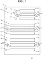
- FIG. 1 shows a generalized top view of a process control monitoring system 20 in accordance with an embodiment.
- Process control monitoring system 20 is generally formed in a structural layer 22 (shown in the side view of FIG. 4 ) on a surface 24 of a substrate 26.
- Process control monitoring system 20 generally includes a first structure 28, a second structure 30, and a third structure 32 formed in structural layer 22.
- First structure 28 includes a first finger 34 interposed between a first pair of sidewalls 36, 38.
- First finger 34 has a first end 40 and a second end 42.
- a first pair of terminals 44, 46 is in electrical communication with first end 40 of first finger 34, and a second pair of terminals 48, 50 is in electrical communication with second end 42.
- a first contact 52 is in electrical communication with sidewall 36 and a second contact 54 is in electrical communication with sidewall 38.
- electrical communication refers to an electrical connection via, for example, conductive traces, bond wires, or any other technique implemented to provide electrical continuity between respective terminals or contacts and their respective structures.
- second structure 30 includes a second finger 56 interposed between a second pair of sidewalls 58, 60.
- Second finger 56 has a first end 62 and a second end 64.
- a first pair of terminals 66, 68 is in electrical communication with first end 62 of second finger 56, and a second pair of terminals 70, 72 is in electrical communication with second end 64.
- a first contact 74 is in electrical communication with sidewall 58 and a second contact 76 is in electrical communication with sidewall 60.
- Third structure 32 includes a third finger 78 interposed between a third pair of sidewalls 80, 82.
- Third finger 78 has a first end 84 and a second end 86.
- a first pair of terminals 88, 90 is in electrical communication with first end 84 of third finger 78, and a second pair of terminals 92, 94 is in electrical communication with second end 86.
- a first contact 96 is in electrical communication with sidewall 80 and a second contact 98 is in electrical communication with sidewall 82.
- First finger 34 is immovable relative to its corresponding first pair of sidewalls 36, 38.
- second finger 56 is immovable relative to its corresponding second pair of sidewalls 58, 60.
- third finger 78 is immovable relative to its corresponding third pair of sidewalls 80, 82. That is first, second, and third fingers 34, 56, 78 and sidewalls 36, 38, 58, 60, 80, 82 are all fixedly (i.e., non-movably) coupled to surface 24 of substrate 26.
- the resistance of each of first, second, and third fingers 34, 56, 78 and the static capacitance between each of first, second, and third fingers 34, 56, 78 and its immediate surroundings can be measured.
- the resistance and capacitance measurements for each of first, second, and third, structures 28, 30, 32 having differing critical dimensions can be utilized to determine critical device parameters (e.g., resistivity, thickness of the structural layer, and amount of undercut of the etched features) resulting from the particular semiconductor fabrication process implemented to form them.
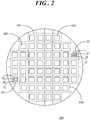
- FIG. 2 shows a simplified top view of a wafer structure 100 that includes a plurality of semiconductor devices 102 and at least one process control monitoring system 20.
- Wafer structure 100 is shown with a number of semiconductor devices 102 formed therein that are separated by scribe lines 104, where each semiconductor device 102 may include a MEMS or MEMS-like structure having a semiconductor layer (e.g., structural layer 22 of FIG. 4 ) and narrow features etched into structural layer 22.
- Semiconductor devices 102 are represented by boxes for simplicity of illustration. However, those skilled in the art will recognize that each of semiconductor devices 102 can include a plurality of movable and non-movable features.
- semiconductor devices 102 and first, second, and third structures 28, 30, 32 of process control monitoring system 20 are concurrently fabricated using the same semiconductor device fabrication process. Accordingly, the critical device parameters extracted utilizing process control monitoring system 20 and methodology described below will apply equivalently to the features of semiconductor devices 102.
- wafer structure 100 can include any suitable quantity of process control monitoring systems 20 distributed across wafer structure 100. Further, the two process control monitoring systems 20 are also shown in areas of wafer structure 100 that are fully surrounded by scribe lines 104. However, process control monitoring systems 20 can be formed at any suitable unused portion of wafer structure 100 since following characterization of the critical parameters and subsequent dicing of wafer structure 100 along scribe lines 104, they will no longer be used.
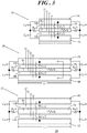
- FIG. 3 shows a top view of the process control monitoring system 20 depicting the resistance and capacitances used to determine the critical device parameters of material resistivity, layer thickness, and amount of undercut of the etched features
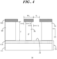
- FIG. 4 shows a cross-sectional side view of second structure 30 of process control monitoring system 20 along section lines 4-4 of FIG. 3 . That is, FIGs. 3 and 4 show generalized sketches of first, second, and third structures 28, 30, 32 that are labeled with the parameters used in the analysis.
- An algorithm described below which may be realized as program code executed by a computing system (not shown), is used to extract the critical device parameters from simple resistance and capacitance measurements on the static (i.e., non-movable) structures 28, 30, 32.
- L is the printed finger length and W is the printed finger width as determined by the original pattern dimension of an etch mask 105, where each of the length and width is parallel to surface 24 of substrate 26 ( FIG. 1 ).
- First finger 34 is separated from each of sidewalls 36, 38 by a gap 106 having a dimension or width referred to herein as a spacing, S.
- second finger 56 is separated from each of sidewalls 58, 60 by a gap 108 having a spacing, S
- third finger 78 is separated from each of sidewalls 80, 82 by a gap 110 having a spacing, S.
- First finger 34 exhibits a first length, L 1 , and a first width, W 1 . Additionally, first finger 34 is separated from each of the adjacent sidewalls 36, 38 by a first spacing, S 1 .
- Second finger 56 exhibits a second length, L 2 , and first width, W 1 . Additionally, second finger 56 is separated from each of the adjacent sidewalls 58, 60 by first spacing, S 1 .
- Third finger 78 exhibits second length, L 2 , and a second width, W 2 . Additionally, third finger 78 is separated from each of the adjacent sidewalls 80, 82 by a second spacing, S 2 .
- first length, L 1 differs from second length, L 2 , first width, W 1 , differs from second width, W 2 , and first spacing, S 1 , differs from second spacing, S 2 .
- a substrate structure may be a silicon on insulator (SOI) wafer that includes a handle substrate 112, a buried oxide layer 114, and a semiconductor layer, referred to herein as structural layer 22.
- SOI silicon on insulator
- the features of semiconductor devices 102 ( FIG. 3 ) and process control monitoring system 20 are formed in structural layer 22.
- each of first, second, and third fingers 34, 56, 78 exhibits a thickness, T, perpendicular to surface 24 of substrate 26 corresponding to the thickness of structural layer 22, where the thickness, T, is generally equivalent for each of the first, second, and third fingers 34, 56, 78.
- the process variables (i.e., critical device parameters) to be monitored utilizing first, second, and third structures 28, 30, 32 include an amount of undercut of the etched features, referred to herein as an etch undercut parameter, D, the resistivity parameter, p, of structural layer 22, and the thickness parameter, T, of structural layer 22.
- R 1 , R 2 , R 3 are the measured resistances and C 1 , C 2 , C 3 are the measured capacitances of first, second, and third structures 28, 30, 32, respectively.
- R 1 , R 2 , R 3 , C 1 , C 2 , C 3 are known since they can be directly measured.
- R P and C P are the parasitic resistance and capacitance, respectively, of first, second, and third structures 28, 30, and 32.
- the system of equations (1), (2), (3), (4), (5), and (6) can be solved by first subtracting pairs of equations to eliminate the measurement parasitics (i.e., R P and C P ).
- R 2 ⁇ R 3 C 2 ⁇ C 3 R 1 ⁇ R 2 C 1 ⁇ C 2 L 2 2 L 1 ⁇ L 2 2 1 ⁇ W 1 ⁇ 2 D W 2 ⁇ 2 D 1 ⁇ S 1 + 2 D S 2 + 2 D
- first, second, and third structures 28, 30, 32 together with the analysis routines form a self-consistent method of extracting the three key physical device parameters of MEMS structural layer resistivity parameter (p), thickness parameter (T), and etch undercut parameter (D) directly from the electrical resistance and capacitance measurements.
- FIG. 5 shows a top view of an example layout 112 of one of the structures of the process control monitoring system 20 ( FIG. 1 ).
- layout 112 includes second structure 30 having second finger 56 interposed between second pair of sidewalls 58, 60.
- first pair of terminals 66, 68, second pair of terminals 70, 72 connected with second finger 56, and first and second contacts 74, 76 connected with second pair of sidewalls 58, 60 are also illustrated in example layout 112.
- An electrically conductive trace 114 interconnects first and second contacts 74, 76, and various electrically conductive input/output (I/O) traces 116 are used to connect first pair of terminals 66, 68, second pair of terminals 70, 72, first contact 74, and second contact 76 to measurement equipment (generally discussed below in connection with FIG. 6 ).
- Layout 112 additionally shows a portion of one of semiconductor devices 102 which may include a combination of movable and nonmovable features (e.g., a comb structure with movable mass) and electrical connections.
- a stippled pattern over much of structural layer 22 indicates a dielectric material overlying the structural features formed within structural layer 22 to yield a buried semiconductor layer. However, the stippled pattern is not shown over second structure 30 for clarity of illustration. It should be understood that the dielectric material may also be disposed between conductive traces 114, 116 and the underlying structural layer 22 to provide suitable electrical isolation between various features.
- FIG. 6 shows a flowchart of a critical parameter characterization process 120 in accordance with another embodiment.
- Critical process characterization process 120 may be implemented in connection with any wafer processing technology (i.e., semiconductor device fabrication process) for which a quantitative assessment of the critical device parameters of resistivity, structural layer thickness, and etch undercut parameters are desired.
- a semiconductor fabrication process that includes operations of, for example, patterning, deposition, and etching is implemented to form wafer structure 100 ( FIG. 2 ) that includes semiconductor devices 102 ( FIG. 2 ) and process control monitoring system 20 ( FIG. 1 ) in structural layer 22 ( FIG. 4 ).
- resistances R 1 , R 2 , R 3 of corresponding first, second, and third fingers 34, 56, 78 are determined.
- R 1 , R 2 , R 3 may be measured utilizing a four-terminal resistance measurement device (e.g., ohmmeter) capable of performing four-lead Kelvin sensing.
- a four-terminal resistance measurement device e.g., ohmmeter
- current may be supplied to first finger 34 via terminals 44, 50 (i.e., the current leads).
- the separation of current and voltage leads eliminates the lead and contact resistance from the measurement, which is advantageous for precise measurement of low resistance values.
- Alternative embodiments may employ a different resistance measurement technique for determining R 1 , R 2 , R 3 .
- static capacitances C 1 , C 2 , C 3 of corresponding first, second, and third structures 28, 30, 32 are determined.
- C 1 , C 2 , C 3 may be measured by utilizing a capacitance measurement device (e.g., an LCR meter).
- a capacitance measurement device e.g., an LCR meter.
- first and second contacts 52, 54 may be connected to the capacitance measurement device at a first potential (HIGH) and first pair of terminals 44, 46 and second pair of terminals 48, 50 may be connected to the capacitance measurement device at a second potential (LOW).
- First structure 28 is thereafter subjected to an alternating current (AC) voltage source.
- AC alternating current
- An LCR meter measures the voltage across and the current through first structure 28. From the ratio of the voltage and current, the LCR meter can determine the magnitude of the impedance. The phase angle between the voltage and current is also measured. The LCR meter can calculate the capacitance from the impedance and the phase angle. Alternative embodiments may employ a different capacitance measurement technique for determining C 1 , C 2 , C 3 .
- the measured resistances, R 1 , R 2 , R 3 , and the measured capacitances, C 1 , C 2 , C 3 are utilized to compute etch undercut parameter, D, resistivity parameter, ⁇ , and thickness parameter, T, as discussed in detail above.
- a computing system executing an algorithm containing the above equations may be utilized to compute etch undercut parameter, resistivity parameter, and thickness parameter.
- Embodiments are described above with a single "finger” per each of the structures (e.g., first structure 28 having first finger 34, second structure 30 having second finger 56, and third structure 32 having third finger 78 as shown in FIG. 1 ) for compactness and simplicity.
- Alternative embodiments may include multiple "fingers" per structure to yield higher measures capacitance values and lower measured resistance values.
- An embodiment of a process control monitoring system formed on a substrate comprises a first structure formed in a structural layer of the substrate, the first structure including a first finger interposed between a first pair of sidewalls, the first finger exhibiting a first length and a first width, each of which is parallel to a surface of the substrate, and the first finger being separated from each of the first pair of sidewalls by a first gap having a first spacing.
- the process control monitoring system further comprises a second structure formed in the structural layer of the substrate, the second structure including a second finger interposed between a second pair of sidewalls, the second finger exhibiting a second length and the first width, each of which is parallel to the surface of the substrate, and the second finger being separated from each of the second pair of sidewalls by a second gap having the first spacing.
- the system process control monitoring comprises a third structure formed in the structural layer of the substrate, the third structure including a third finger interposed between a third pair of sidewalls, the third finger exhibiting the second length and a second width, each of which is parallel to the surface of the substrate, and the third finger being separated from each of the third pair of sidewalls by a third gap having a second spacing.
- An embodiment of a method of characterizing critical parameters resulting from a semiconductor device fabrication process comprises implementing the semiconductor device fabrication process to form a process control monitoring system in a structural layer of a substrate.
- the process control monitoring system includes a first structure including a first finger interposed between a first pair of sidewalls, the first finger exhibiting a first length and a first width, each of which is parallel to a surface of the substrate, and the first finger being separated from each of the first pair of sidewalls by a first gap having a first spacing.
- the process control monitoring system further includes a second structure including a second finger interposed between a second pair of sidewalls, the second finger exhibiting a second length and the first width, each of which is parallel to the surface of the substrate, and the second finger being separated from each of the second pair of sidewalls by a second gap having the first spacing.
- the process control monitoring system further includes a third structure including a third finger interposed between a third pair of sidewalls, the third finger exhibiting the second length and a second width, each of which is parallel to the surface of the substrate, and the third finger being separated from each of the third pair of sidewalls by a third gap having a second spacing.
- the method further comprises determining the critical parameters based on the first and second lengths, the first and second widths, and the first and second spacings for associated ones of the first, second, and third fingers.
- An embodiment of a wafer structure comprises a substrate, a plurality of semiconductor devices formed in a structural layer of the substrate, and a process control monitoring system formed in a structural layer of the substrate, wherein the plurality of semiconductor devices and the process control monitoring system are fabricated concurrently using the same semiconductor device fabrication process.
- the process control monitoring system includes a first structure including a first finger interposed between a first pair of sidewalls, the first finger exhibiting a first length and a first width, each of which is parallel to a surface of the substrate, and the first finger being separated from each of the first pair of sidewalls by a first gap having a first spacing.
- the process control monitoring system further includes a second structure including a second finger interposed between a second pair of sidewalls, the second finger exhibiting a second length and the first width, each of which is parallel to the surface of the substrate, and the second finger being separated from each of the second pair of sidewalls by a second gap having the first spacing.
- the process control monitoring system further includes a third structure including a third finger interposed between a third pair of sidewalls, the third finger exhibiting the second length and a second width, each of which is parallel to the surface of the substrate, and the third finger being separated from each of the third pair of sidewalls by a third gap having a second spacing.
- the first and second lengths, the first and second widths, and the first and second spacings for associated ones of the first, second, and third fingers are utilized to determine critical parameters of the plurality of the semiconductor devices resulting from the semiconductor device fabrication process.
- the embodiments described herein enable the extraction of critical device parameters with a self-consistent analysis of the resistance and capacitance measurements on the structures in which these critical parameters are coupled. Further, these critical parameters are effectively decoupled by the simultaneous solution of coupled equations describing the resistance and capacitance measurements on the different structures. Accordingly, the resistance and capacitance measurements enable electrical characterization of, for example, a product wafer, in order to extract the critical device parameters of the electrical resistivity of the structural layer, the thickness of the structural layer, and the amount of undercut of the etched features.
- the system and associated methodology enables the extraction of these critical device parameters without the need for sacrificial wafers, cross sectioning, or the use of complex SEM analysis. Accordingly, variations in resistivity, material thickness, and amount of undercut can be readily monitored in order to optimize production yields, device performance, and the quality of semiconductor devices, such as microelectromechanical systems (MEMS) devices.
- MEMS microelectromechanical systems
Landscapes
- Engineering & Computer Science (AREA)
- Physics & Mathematics (AREA)
- General Physics & Mathematics (AREA)
- Microelectronics & Electronic Packaging (AREA)
- Manufacturing & Machinery (AREA)
- Automation & Control Theory (AREA)
- Environmental & Geological Engineering (AREA)
- Computer Hardware Design (AREA)
- General Engineering & Computer Science (AREA)
- Testing Or Measuring Of Semiconductors Or The Like (AREA)
- Semiconductor Integrated Circuits (AREA)
Abstract
Description
- The present invention relates generally to semiconductor device fabrication processes. More specifically, the present invention relates to a system and method for characterizing critical parameters of a device manufactured in accordance with a semiconductor device fabrication process.
- Microelectromechanical systems (MEMS) technology provides a way to make very small mechanical structures and integrate these structures with electrical devices on a single substrate using conventional batch semiconductor processing techniques. One common application of MEMS is the design and manufacture of sensor devices. MEMS sensor devices are widely used in applications such as automotive, inertial guidance systems, household appliances, game devices, protection systems for a variety of devices, and many other industrial, scientific, and engineering systems.
- Conventional MEMS fabrication processes typically employ a slab (i.e., structural layer) of semiconductor material of a given resistivity and thickness into which features are etched to form electromechanical structures that perform the desired functions needed to realize MEMS devices, such as accelerometers and gyroscopes. The critical device parameters include, for example, the electrical resistivity of the structural layer, the thickness of the structural layer, and the width of the etched features in which the width is determined by the original mask pattern dimension and the amount of undercut incurred during the etch process. All three of these key critical parameters (i.e., resistivity, thickness, and amount of undercut) typically vary slightly across a wafer, wafer to wafer, and/or process lot to process lot. Due to these variations, it may be necessary to routinely monitor these critical parameters in order to optimize production yields, device performance, and quality of the MEMS devices.
- Some prior art techniques electrically measure the sheet resistance of the MEMS structural layer by using conventional van der Pauw patterns or Kelvined resistor structures. However, to determine the local resistivity of the structural layer, the layer thickness and/or the lateral geometries of the structures must be accurately known. Because the lateral dimensions (and their variations of interest) of typical MEMS features is on the order of a micron or less, it is not typically feasible to use optical microscopy. Accordingly, more complex Scanning Electron Microscopy (SEM) inspections are needed to obtain the lateral physical dimensions. Furthermore, in order to obtain the local structural layer thickness uniformity information, a wafer must be sacrificed for cross section and multiple measurements are thereafter performed along this cross section. Thus, it is not practically and cost effectively feasible to routinely map wafers with this approach. Nor does it provide data from the actual product wafers where such date would be of greatest value.
- Other prior art techniques utilize capacitance measurement on some type of dynamically driven, oscillating or resonance MEMS structures. Capacitance measurements on these movable structures involve complex, sophisticated testing techniques and may involve comparison to numerical analysis and simulations. Further, these techniques are primarily focused on extracting the lateral dimensions of a MEMS features (more specifically, amount of etch undercut) and assume that the thickness of the structural layer is known. In actually, the thickness of the structural layer and the gap (which includes etch undercut) are coupled together in the capacitance measurement.
- The accompanying figures in which like reference numerals refer to identical or functionally similar elements throughout the separate views, the figures are not necessarily drawn to scale, and which together with the detailed description below are incorporated in and form part of the specification, serve to further illustrate various embodiments and to explain various principles and advantages all in accordance with the present invention.
-
FIG. 1 shows a generalized top view of a process control monitoring system in accordance with an embodiment; -
FIG. 2 shows a simplified top view of a wafer structure that includes a plurality of semiconductor devices and at least one process control monitoring system ofFIG. 1 ; -
FIG. 3 shows a top view of the process control monitoring system ofFIG. 1 depicting the resistance and capacitances used to determine the critical device parameters; -
FIG. 4 shows a cross-sectional side view of one of the structures of the process control monitoring system along section lines 4-4 ofFIG. 3 ; -
FIG. 5 shows a top view of an example layout of one of the structures of the process control monitoring system; and -
FIG. 6 shows a flowchart of a critical parameter characterization process in accordance with another embodiment. - In overview, embodiments disclosed herein entail a process control monitoring system and a method for characterizing critical device parameters resulting from a semiconductor device fabrication process, where the semiconductor device fabrication process is utilized to form the process control monitoring system as well as a plurality of semiconductor devices in a structural layer of the substrate. The process control monitoring system includes three related structures, but with different critical dimensions. The general configuration of each of the three structures includes a single fixed "finger" of a given width and length etched into a structural layer of a given thickness. On each side of the finger, there is a given spacing to adjacent sidewalls of the structural layer. Various electrical contacts are made to the finger and to the adjacent sidewalls of the structural layer in order to obtain a resistance measurement of the finger and to measure a static, differential capacitance between the finger and the surrounding sidewalls. The resistance and capacitance measurements enable electrical characterization of, for example, a product wafer, in order to extract the critical device parameters of the electrical resistivity of the structural layer, the thickness of the structural layer, and the amount of undercut of the etched features. The system and associated methodology enables the extraction of these critical device parameters without the need for sacrificial wafers, cross sectioning, or the use of complex SEM analysis. Accordingly, variations in resistivity, material thickness, and amount of undercut can be readily monitored in order to optimize production yields, device performance, and the quality of semiconductor devices, such as microelectromechanical systems (MEMS) devices.
- The instant disclosure is provided to further explain in an enabling fashion the best modes, at the time of the application, of making and using various embodiments in accordance with the present invention. The disclosure is further offered to enhance an understanding and appreciation for the inventive principles and advantages thereof, rather than to limit in any manner the invention. The invention is defined solely by the appended claims including any amendments made during the pendency of this application and all equivalents of those claims as issued.
- It should be understood that the use of relational terms, if any, such as first and second, top and bottom, and the like are used solely to distinguish one from another entity or action without necessarily requiring or implying any actual such relationship or order between such entities or actions. Furthermore, some of the figures may be illustrated using various shading and/or hatching to distinguish the different elements produced within the various structural layers. These different elements within the structural layers may be produced utilizing current and upcoming microfabrication techniques of depositing, patterning, etching, and so forth. Accordingly, although different shading and/or hatching is utilized in the illustrations, the different elements within the structural layers may be formed out of the same material.
- Referring to
FIG. 1, FIG. 1 shows a generalized top view of a processcontrol monitoring system 20 in accordance with an embodiment. Processcontrol monitoring system 20 is generally formed in a structural layer 22 (shown in the side view ofFIG. 4 ) on asurface 24 of asubstrate 26. Processcontrol monitoring system 20 generally includes afirst structure 28, asecond structure 30, and athird structure 32 formed instructural layer 22. -
First structure 28 includes afirst finger 34 interposed between a first pair ofsidewalls First finger 34 has afirst end 40 and asecond end 42. A first pair ofterminals first end 40 offirst finger 34, and a second pair ofterminals second end 42. In addition, afirst contact 52 is in electrical communication withsidewall 36 and asecond contact 54 is in electrical communication withsidewall 38. The term "electrical communication" refers to an electrical connection via, for example, conductive traces, bond wires, or any other technique implemented to provide electrical continuity between respective terminals or contacts and their respective structures. - Similarly,
second structure 30 includes asecond finger 56 interposed between a second pair ofsidewalls Second finger 56 has afirst end 62 and asecond end 64. A first pair ofterminals first end 62 ofsecond finger 56, and a second pair ofterminals second end 64. In addition, afirst contact 74 is in electrical communication withsidewall 58 and asecond contact 76 is in electrical communication withsidewall 60. -
Third structure 32 includes athird finger 78 interposed between a third pair ofsidewalls Third finger 78 has afirst end 84 and asecond end 86. A first pair ofterminals first end 84 ofthird finger 78, and a second pair ofterminals second end 86. In addition, afirst contact 96 is in electrical communication withsidewall 80 and a second contact 98 is in electrical communication withsidewall 82. -
First finger 34 is immovable relative to its corresponding first pair ofsidewalls second finger 56 is immovable relative to its corresponding second pair ofsidewalls third finger 78 is immovable relative to its corresponding third pair ofsidewalls third fingers substrate 26. - As will be discussed in significantly greater detail below, the resistance of each of first, second, and
third fingers third fingers structures - Referring now to
FIG. 2, FIG. 2 shows a simplified top view of awafer structure 100 that includes a plurality ofsemiconductor devices 102 and at least one processcontrol monitoring system 20.Wafer structure 100 is shown with a number ofsemiconductor devices 102 formed therein that are separated byscribe lines 104, where eachsemiconductor device 102 may include a MEMS or MEMS-like structure having a semiconductor layer (e.g.,structural layer 22 ofFIG. 4 ) and narrow features etched intostructural layer 22.Semiconductor devices 102 are represented by boxes for simplicity of illustration. However, those skilled in the art will recognize that each ofsemiconductor devices 102 can include a plurality of movable and non-movable features. In accordance with an embodiment,semiconductor devices 102 and first, second, andthird structures control monitoring system 20 are concurrently fabricated using the same semiconductor device fabrication process. Accordingly, the critical device parameters extracted utilizing processcontrol monitoring system 20 and methodology described below will apply equivalently to the features ofsemiconductor devices 102. - In this example, two process
control monitoring systems 20 are shown. However,wafer structure 100 can include any suitable quantity of processcontrol monitoring systems 20 distributed acrosswafer structure 100. Further, the two processcontrol monitoring systems 20 are also shown in areas ofwafer structure 100 that are fully surrounded byscribe lines 104. However, processcontrol monitoring systems 20 can be formed at any suitable unused portion ofwafer structure 100 since following characterization of the critical parameters and subsequent dicing ofwafer structure 100 alongscribe lines 104, they will no longer be used. - Referring to
FIGS. 3 and4 ,FIG. 3 shows a top view of the processcontrol monitoring system 20 depicting the resistance and capacitances used to determine the critical device parameters of material resistivity, layer thickness, and amount of undercut of the etched features andFIG. 4 shows a cross-sectional side view ofsecond structure 30 of processcontrol monitoring system 20 along section lines 4-4 ofFIG. 3 . That is,FIGs. 3 and4 show generalized sketches of first, second, andthird structures structures - In the sketches provided in
FIGs. 3 and4 , L is the printed finger length and W is the printed finger width as determined by the original pattern dimension of anetch mask 105, where each of the length and width is parallel to surface 24 of substrate 26 (FIG. 1 ).First finger 34 is separated from each ofsidewalls gap 106 having a dimension or width referred to herein as a spacing, S. Likewise,second finger 56 is separated from each ofsidewalls gap 108 having a spacing, S, andthird finger 78 is separated from each ofsidewalls gap 110 having a spacing, S. -
First finger 34 exhibits a first length, L1, and a first width, W1. Additionally,first finger 34 is separated from each of theadjacent sidewalls second finger 56 is separated from each of theadjacent sidewalls third finger 78 is separated from each of theadjacent sidewalls - As exemplified in
FIG. 4 , a substrate structure may be a silicon on insulator (SOI) wafer that includes ahandle substrate 112, a buriedoxide layer 114, and a semiconductor layer, referred to herein asstructural layer 22. The features of semiconductor devices 102 (FIG. 3 ) and processcontrol monitoring system 20 are formed instructural layer 22. Thus, each of first, second, andthird fingers substrate 26 corresponding to the thickness ofstructural layer 22, where the thickness, T, is generally equivalent for each of the first, second, andthird fingers - With continued reference to
FIGs. 3 and4 , the process variables (i.e., critical device parameters) to be monitored utilizing first, second, andthird structures structural layer 22, and the thickness parameter, T, ofstructural layer 22. R1, R2, R3 are the measured resistances and C1, C2, C3 are the measured capacitances of first, second, andthird structures third structures - R1 and C1 can be characterized by the following equations:


- Similarly, R2 and C2 can be characterized by the following equations:


- And, R3 and C3 can be characterized by the following equations:


- The system of equations (1), (2), (3), (4), (5), and (6) can be solved by first subtracting pairs of equations to eliminate the measurement parasitics (i.e., RP and CP). The parasitics can be eliminated from the length variation structures as follows:


- Then the parasitics can be eliminated from the width variation structures as follows:


- The RC products of equations (7) and (8) eliminates the thickness parameter, T, as follows:

- Solving equation (11) for the resistivity parameter, p, yields an equation (12) in the last remaining variable, i.e., the etch undercut parameter, D, which can be used to solve for resistivity parameter, p, after etch undercut parameter, D is determined.

- To solve for the etch undercut parameter, D, the RC product of equations (9) and (10) is determined to again eliminate the thickness parameter, T, as follows:

- Now substituting for the resistivity parameter, p, from equation (12) yields the following:

- Distributing the two numerator factors containing, etch undercut parameter, D, into the two bracketed terms gives:

- Note that the form of equation (15) implies that if either of the two widths or the two spacings are identical (i.e., W1=W2 or S1=S2) then the analysis becomes invalid. Continuing the numerical analysis:


- And continuing the expansion:


- Now rearranging and putting into standard quadratic form:


- In some embodiments, the width, W, and the spacing, S, are equivalent. That is, the first width is equivalent to the first spacing (W1=S1=X1) and the second width is equivalent to the second spacing (W2=S2=X2), but W1 is different from W2 and S1 is different from S2 amongst first, second, and
third structures 

- Once the etch undercut parameter, D, has been computed from either of equations (22) or (24), then the resistivity parameter, p, can be determined from equation (12), and the thickness parameter, T, can be determined from either of equations (7), (8), (9), or (10). Most accurately, however, the thickness parameter, T, can be determined from equation (8), as follows:

- As demonstrated above, the judiciously selected first and second lengths, first and second widths, and first and second widths for associated ones of first, second, and
third fingers third structures -
FIG. 5 shows a top view of anexample layout 112 of one of the structures of the process control monitoring system 20 (FIG. 1 ). In this example,layout 112 includessecond structure 30 havingsecond finger 56 interposed between second pair ofsidewalls terminals terminals second finger 56, and first andsecond contacts sidewalls 58, 60 (as described above) are also illustrated inexample layout 112. An electricallyconductive trace 114 interconnects first andsecond contacts terminals terminals first contact 74, andsecond contact 76 to measurement equipment (generally discussed below in connection withFIG. 6 ).Layout 112 additionally shows a portion of one ofsemiconductor devices 102 which may include a combination of movable and nonmovable features (e.g., a comb structure with movable mass) and electrical connections. - A stippled pattern over much of
structural layer 22 indicates a dielectric material overlying the structural features formed withinstructural layer 22 to yield a buried semiconductor layer. However, the stippled pattern is not shown oversecond structure 30 for clarity of illustration. It should be understood that the dielectric material may also be disposed betweenconductive traces structural layer 22 to provide suitable electrical isolation between various features. -
FIG. 6 shows a flowchart of a criticalparameter characterization process 120 in accordance with another embodiment. Criticalprocess characterization process 120 may be implemented in connection with any wafer processing technology (i.e., semiconductor device fabrication process) for which a quantitative assessment of the critical device parameters of resistivity, structural layer thickness, and etch undercut parameters are desired. - At a
block 122, a semiconductor fabrication process that includes operations of, for example, patterning, deposition, and etching is implemented to form wafer structure 100 (FIG. 2 ) that includes semiconductor devices 102 (FIG. 2 ) and process control monitoring system 20 (FIG. 1 ) in structural layer 22 (FIG. 4 ). - At a
block 124, resistances R1, R2, R3 of corresponding first, second, andthird fingers first structure 28 shown inFIG. 1 , current may be supplied tofirst finger 34 viaterminals 44, 50 (i.e., the current leads). The resulting voltage can be measured betweenterminals 46, 48 (i.e., voltage leads) and the resistance can be extracted via Ohm's Law, V=IR. The separation of current and voltage leads eliminates the lead and contact resistance from the measurement, which is advantageous for precise measurement of low resistance values. Alternative embodiments may employ a different resistance measurement technique for determining R1, R2, R3. - At a
block 126, static capacitances C1, C2, C3 of corresponding first, second, andthird structures FIG. 1 ) are determined. By way of example, C1, C2, C3 may be measured by utilizing a capacitance measurement device (e.g., an LCR meter). Again referring tofirst structure 28 shown inFIG. 1 , first andsecond contacts terminals terminals First structure 28 is thereafter subjected to an alternating current (AC) voltage source. An LCR meter measures the voltage across and the current throughfirst structure 28. From the ratio of the voltage and current, the LCR meter can determine the magnitude of the impedance. The phase angle between the voltage and current is also measured. The LCR meter can calculate the capacitance from the impedance and the phase angle. Alternative embodiments may employ a different capacitance measurement technique for determining C1, C2, C3. - At a
block 128 the measured resistances, R1, R2, R3, and the measured capacitances, C1, C2, C3, are utilized to compute etch undercut parameter, D, resistivity parameter, ρ, and thickness parameter, T, as discussed in detail above. Again, a computing system executing an algorithm containing the above equations may be utilized to compute etch undercut parameter, resistivity parameter, and thickness parameter. These computed critical parameters can be utilized in order optimize production yields, device performance, and quality of the semiconductor devices. Thereafter, critical parameter characterization process ends. - Embodiments are described above with a single "finger" per each of the structures (e.g.,
first structure 28 havingfirst finger 34,second structure 30 havingsecond finger 56, andthird structure 32 havingthird finger 78 as shown inFIG. 1 ) for compactness and simplicity. Alternative embodiments may include multiple "fingers" per structure to yield higher measures capacitance values and lower measured resistance values. - Thus, a process control monitoring system and a method of characterizing critical parameters resulting from a semiconductor device fabrication process are discloses herein. An embodiment of a process control monitoring system formed on a substrate comprises a first structure formed in a structural layer of the substrate, the first structure including a first finger interposed between a first pair of sidewalls, the first finger exhibiting a first length and a first width, each of which is parallel to a surface of the substrate, and the first finger being separated from each of the first pair of sidewalls by a first gap having a first spacing. The process control monitoring system further comprises a second structure formed in the structural layer of the substrate, the second structure including a second finger interposed between a second pair of sidewalls, the second finger exhibiting a second length and the first width, each of which is parallel to the surface of the substrate, and the second finger being separated from each of the second pair of sidewalls by a second gap having the first spacing. And the system process control monitoring comprises a third structure formed in the structural layer of the substrate, the third structure including a third finger interposed between a third pair of sidewalls, the third finger exhibiting the second length and a second width, each of which is parallel to the surface of the substrate, and the third finger being separated from each of the third pair of sidewalls by a third gap having a second spacing.
- An embodiment of a method of characterizing critical parameters resulting from a semiconductor device fabrication process comprises implementing the semiconductor device fabrication process to form a process control monitoring system in a structural layer of a substrate. The process control monitoring system includes a first structure including a first finger interposed between a first pair of sidewalls, the first finger exhibiting a first length and a first width, each of which is parallel to a surface of the substrate, and the first finger being separated from each of the first pair of sidewalls by a first gap having a first spacing. The process control monitoring system further includes a second structure including a second finger interposed between a second pair of sidewalls, the second finger exhibiting a second length and the first width, each of which is parallel to the surface of the substrate, and the second finger being separated from each of the second pair of sidewalls by a second gap having the first spacing. And, the process control monitoring system further includes a third structure including a third finger interposed between a third pair of sidewalls, the third finger exhibiting the second length and a second width, each of which is parallel to the surface of the substrate, and the third finger being separated from each of the third pair of sidewalls by a third gap having a second spacing. The method further comprises determining the critical parameters based on the first and second lengths, the first and second widths, and the first and second spacings for associated ones of the first, second, and third fingers.
- An embodiment of a wafer structure comprises a substrate, a plurality of semiconductor devices formed in a structural layer of the substrate, and a process control monitoring system formed in a structural layer of the substrate, wherein the plurality of semiconductor devices and the process control monitoring system are fabricated concurrently using the same semiconductor device fabrication process. The process control monitoring system includes a first structure including a first finger interposed between a first pair of sidewalls, the first finger exhibiting a first length and a first width, each of which is parallel to a surface of the substrate, and the first finger being separated from each of the first pair of sidewalls by a first gap having a first spacing. The process control monitoring system further includes a second structure including a second finger interposed between a second pair of sidewalls, the second finger exhibiting a second length and the first width, each of which is parallel to the surface of the substrate, and the second finger being separated from each of the second pair of sidewalls by a second gap having the first spacing. And the process control monitoring system further includes a third structure including a third finger interposed between a third pair of sidewalls, the third finger exhibiting the second length and a second width, each of which is parallel to the surface of the substrate, and the third finger being separated from each of the third pair of sidewalls by a third gap having a second spacing. The first and second lengths, the first and second widths, and the first and second spacings for associated ones of the first, second, and third fingers are utilized to determine critical parameters of the plurality of the semiconductor devices resulting from the semiconductor device fabrication process.
- The embodiments described herein enable the extraction of critical device parameters with a self-consistent analysis of the resistance and capacitance measurements on the structures in which these critical parameters are coupled. Further, these critical parameters are effectively decoupled by the simultaneous solution of coupled equations describing the resistance and capacitance measurements on the different structures. Accordingly, the resistance and capacitance measurements enable electrical characterization of, for example, a product wafer, in order to extract the critical device parameters of the electrical resistivity of the structural layer, the thickness of the structural layer, and the amount of undercut of the etched features. The system and associated methodology enables the extraction of these critical device parameters without the need for sacrificial wafers, cross sectioning, or the use of complex SEM analysis. Accordingly, variations in resistivity, material thickness, and amount of undercut can be readily monitored in order to optimize production yields, device performance, and the quality of semiconductor devices, such as microelectromechanical systems (MEMS) devices.
- This disclosure is intended to explain how to fashion and use various embodiments in accordance with the invention rather than to limit the true, intended, and fair scope and spirit thereof. The foregoing description is not intended to be exhaustive or to limit the invention to the precise form disclosed. Modifications or variations are possible in light of the above teachings. The embodiment(s) was chosen and described to provide the best illustration of the principles of the invention and its practical application, and to enable one of ordinary skill in the art to utilize the invention in various embodiments and with various modifications as are suited to the particular use contemplated. All such modifications and variations are within the scope of the invention as determined by the appended claims, as may be amended during the pendency of this application for patent, and all equivalents thereof, when interpreted in accordance with the breadth to which they are fairly, legally, and equitably entitled.
Claims (15)
- A process control monitoring system formed on a substrate comprising:a first structure (28) formed in a structural layer (22) of said substrate (26), said first structure (28) including a first finger (34) interposed between a first pair of sidewalls (36, 38), said first finger (34) exhibiting a first length (L1) and a first width (W1), each of which is parallel to a surface (24) of said substrate (26), and said first finger (34) being separated from each of said first pair of sidewalls (36, 38) by a first gap (106) having a first spacing (S1);a second structure (30) formed in said structural layer (22) of said substrate (26), said second structure (30) including a second finger (56) interposed between a second pair of sidewalls (58, 60), said second finger (56) exhibiting a second length (L2) and said first width (W1), each of which is parallel to said surface (24) of said substrate (26), and said second finger (56) being separated from each of said second pair of sidewalls (58, 60) by a second gap (108) having said first spacing (S1); anda third structure (32) formed in said structural layer (22) of said substrate (26), said third structure (32) including a third finger (78) interposed between a third pair of sidewalls (80, 82), said third finger (78) exhibiting said second length (L2) and a second width (W2), each of which is parallel to said surface (24) of said substrate (26), and said third finger (78) being separated from each of said third pair of sidewalls (80, 82) by a third gap (110) having a second spacing (S2).
- The process control monitoring system of claim 1, wherein:said first length (L1) differs from said second length (L2);said first width (W1) differs from said second width (W2); andsaid first spacing (S1) differs from said second spacing (S2).
- The process control monitoring system of claim 2, wherein:said first width (W1) is equivalent to said first spacing (S1); andsaid second width (W2) is equivalent to said second spacing (S2).
- The process control monitoring system of any one of the claims 1 to 3, wherein each of said first, second, and third fingers (34, 56, 78) exhibits a thickness perpendicular to said surface (24) of said substrate (26), said thickness being equivalent for said each of said first, second, and third fingers (34, 56, 78).
- The process control monitoring system of any one of the claim 1 to 4, wherein said first, second, and third fingers (34, 56, 78) are immovable relative to corresponding said first, second, and third pairs of sidewalls (36, 38, 58, 60, 80, 82).
- The process control monitoring system of any one of the claim 1 to 5, wherein:each of said first, second, and third fingers (34, 56, 78) includes a first end (40, 62, 84) and a second end (42, 64, 86); andfor said each of said first, second, and third fingers (34, 56, 78), said process control monitoring system (20) further comprises a first pair of terminals (44, 46, 66, 68, 88, 90) in electrical communication with said first end (40, 62, 84) and a second pair of terminals (48, 50, 70, 72, 92, 94) in electrical communication with said second end (42, 64, 86), said first and second pair of terminals (44, 46, 66, 68, 88, 90, 48, 50, 70, 72, 92, 94) being configured for connection with a four terminal resistance measurement device to determine a resistance of said each of said first, second, and third fingers (34, 56, 78).
- The process control monitoring system of claim 6, wherein:each of said first, second, and third pairs of sidewalls (36, 38, 58, 60, 80, 82) includes a first sidewall (36, 58, 80) and a second sidewall (38, 60, 82); andfor said each of said first, second, and third pairs of sidewalls (36, 38, 58, 60, 80, 82), said process control monitoring system (20) further comprises a first contact (52, 74, 96) and a second contact (54, 76, 98), said first contact (52, 74, 96) being in electrical communication with said first sidewall (36, 58, 80), and said second contact (54, 76, 98) being in electrical communication with said second sidewall (38, 60, 82), wherein said first and second electrical contacts (52, 74, 96, 54, 76, 98) are configured for connection with a capacitance measurement device at a first potential and said first and second pairs of terminals are further configured for connection with said capacitance measurement device at a second potential for determining a capacitance between said each of said first, second, and third fingers (34, 56, 78) and associated said each of said first, second, and third pairs of sidewalls (36, 38, 58, 60, 80, 82).
- The process control monitoring system of any one of the claims 1 to 7, wherein said first and second lengths (L1, L2), said first and second widths (W1, W2), and said first and second spacings (S1, S2) for associated ones of said first, second, and third fingers (34, 56, 78) are utilized to determine
an etch undercut parameter (D) of said first, second, and third fingers (34, 56, 78);
a resistivity parameter (p) of said substrate (26); and/or
a thickness parameter (T) of said structural layer (22) perpendicular to said surface (24) of said substrate (26). - A wafer structure including the process control monitoring system of any one of the claims 1 to 8, wherein said wafer structure (100) further comprises a plurality of semiconductor devices (102) formed in said structural layer (22), said process control monitoring system (20) and said plurality of semiconductor devices (102) being fabricated concurrently using the same semiconductor device fabrication process.
- A method of characterizing critical parameters resulting from a semiconductor device fabrication process comprising:Implementing (122) said semiconductor device fabrication process to form a process control monitoring system (20) in a structural layer (22) of a substrate (26), said process control monitoring system (20) including:a first structure (28) including a first finger (34) interposed between a first pair of sidewalls (36, 38), said first finger (34) exhibiting a first length (L1) and a first width (W1), each of which is parallel to a surface (24) of said substrate (26), and said first finger (34) being separated from each of said first pair of sidewalls (36, 38) by a first gap (106) having a first spacing (S1);a second structure (30) including a second finger (56) interposed between a second pair of sidewalls (58, 60), said second finger (56) exhibiting a second length (L2) and said first width (W1), each of which is parallel to said surface (24) of said substrate (26), and said second finger (56) being separated from each of said second pair of sidewalls (58, 60) by a second gap (108) having said first spacing (S1); anda third structure (32) including a third finger (78) interposed between a third pair of sidewalls (80, 82), said third finger (78) exhibiting said second length (L2) and a second width (W2), each of which is parallel to said surface (24) of said substrate (26), and said third finger (78) being separated from each of said third pair of sidewalls (80, 82) by a third gap having a second spacing (S2); anddetermining (124, 126) said critical parameters based on said first and second lengths (L1, L2), said first and second widths (W1, W2), and said first and second spacings (S1, S2) for associated ones of said first, second, and third fingers (34, 56, 78).
- The method of claim 10, wherein said implementing operation (122) forms said process control monitoring system (20) to have said first, second, third fingers (34, 56, 78) that are immovable relative to corresponding said first, second, and third pairs of sidewalls (36, 38, 58, 60, 80, 82).
- The method of claim 10 or claim 11, wherein said determining (124, 126) comprises:determining (124) a first resistance (R1) of said first finger (34);determining (126) a first capacitance (C1) between said first pair of sidewalls (36, 38) and said first finger (34);determining (124) a second resistance (R2) of said second finger (56);determining (126) a second capacitance (C2) between said second pair of sidewalls (58, 60) and second first finger (34);determining (124) a third resistance (R3) of said third finger (78);determining (126) a third capacitance (C3) between said third pair of sidewalls (80, 82) and third first finger (34); andcomputing (128) said critical parameters based on said first, second, and third resistances (R1, R2, R3) and said first, second, and third capacitances (C1, C2, C3).
- The method of claim 12, wherein said determining each of said first, second, and third resistances (R1, R2, R3) comprises measuring a Kelvin resistance of said each of said first, second, and third fingers (34, 56, 78).
- The method of claim 12 or claim 13, wherein said computing operation (128) comprises:computing an etch undercut parameter (D);computing a resistivity parameter (p) of said substrate (26); andcomputing a thickness parameter (T) of said structural layer (22) perpendicular to said surface (24) of said substrate (26), said etch undercut parameter (D), said resistivity parameter (p), and said thickness parameter (T) being said critical parameters, and each of said etch undercut parameter (D), said resistivity parameter (p), and said thickness parameter (T) being computed utilizing said first, second, and third resistances (R1, R2, R3) and said first, second, and third capacitances (C1, C2, C3).
- The method of any one of the claims 10 to 14, further comprising implementing said semiconductor device fabrication process to produce a wafer structure (100) that includes said process control monitoring system (20) and a plurality of semiconductor devices (102) in said structural layer (22), wherein said critical parameters determined utilizing said first, second, and third structures (28, 30, 32) of said process control monitoring system (20) characterizes said critical parameters of said plurality of said semiconductor devices (102).
Applications Claiming Priority (1)
| Application Number | Priority Date | Filing Date | Title |
|---|---|---|---|
| US15/240,701 US20180053698A1 (en) | 2016-08-18 | 2016-08-18 | System and method for characterizing critical parameters resulting from a semiconductor device fabrication process |
Publications (2)
| Publication Number | Publication Date |
|---|---|
| EP3284715A1 true EP3284715A1 (en) | 2018-02-21 |
| EP3284715B1 EP3284715B1 (en) | 2019-08-28 |
Family
ID=58873623
Family Applications (1)
| Application Number | Title | Priority Date | Filing Date |
|---|---|---|---|
| EP17172327.3A Active EP3284715B1 (en) | 2016-08-18 | 2017-05-22 | System and method for characterizing critical parameters resulting from a semiconductor device fabrication process |
Country Status (3)
| Country | Link |
|---|---|
| US (1) | US20180053698A1 (en) |
| EP (1) | EP3284715B1 (en) |
| CN (1) | CN107758609A (en) |
Citations (2)
| Publication number | Priority date | Publication date | Assignee | Title |
|---|---|---|---|---|
| US20030022397A1 (en) * | 2001-07-26 | 2003-01-30 | Hess Jeffery S. | Monitoring and test structures for silicon etching |
| US7935965B1 (en) * | 2008-05-16 | 2011-05-03 | Pdf Solutions, Inc. | Test structures and methods for electrical characterization of alignment of line patterns defined with double patterning |
Family Cites Families (8)
| Publication number | Priority date | Publication date | Assignee | Title |
|---|---|---|---|---|
| US3500066A (en) * | 1968-01-10 | 1970-03-10 | Bell Telephone Labor Inc | Radio frequency power transistor with individual current limiting control for thermally isolated regions |
| US3535600A (en) * | 1968-10-10 | 1970-10-20 | Gen Electric | Mos varactor diode |
| US6542829B1 (en) * | 1999-09-22 | 2003-04-01 | Coventor, Inc. | Characterization of microelectromechanical structures |
| US6750152B1 (en) * | 1999-10-01 | 2004-06-15 | Delphi Technologies, Inc. | Method and apparatus for electrically testing and characterizing formation of microelectric features |
| US8770050B2 (en) * | 2006-03-17 | 2014-07-08 | Jason Vaughn Clark | Method of measuring micro- and nano-scale properties |
| US7355201B2 (en) * | 2006-06-27 | 2008-04-08 | Advanced Micro Devices, Inc. | Test structure for measuring electrical and dimensional characteristics |
| US7592827B1 (en) * | 2007-01-12 | 2009-09-22 | Pdf Solutions, Inc. | Apparatus and method for electrical detection and localization of shorts in metal interconnect lines |
| US7525304B1 (en) * | 2007-05-14 | 2009-04-28 | Kla-Tencor Corporation | Measurement of effective capacitance |
-
2016
- 2016-08-18 US US15/240,701 patent/US20180053698A1/en not_active Abandoned
-
2017
- 2017-05-22 EP EP17172327.3A patent/EP3284715B1/en active Active
- 2017-08-18 CN CN201710716062.6A patent/CN107758609A/en active Pending
Patent Citations (2)
| Publication number | Priority date | Publication date | Assignee | Title |
|---|---|---|---|---|
| US20030022397A1 (en) * | 2001-07-26 | 2003-01-30 | Hess Jeffery S. | Monitoring and test structures for silicon etching |
| US7935965B1 (en) * | 2008-05-16 | 2011-05-03 | Pdf Solutions, Inc. | Test structures and methods for electrical characterization of alignment of line patterns defined with double patterning |
Also Published As
| Publication number | Publication date |
|---|---|
| CN107758609A (en) | 2018-03-06 |
| EP3284715B1 (en) | 2019-08-28 |
| US20180053698A1 (en) | 2018-02-22 |
Similar Documents
| Publication | Publication Date | Title |
|---|---|---|
| US4516071A (en) | Split-cross-bridge resistor for testing for proper fabrication of integrated circuits | |
| US5512836A (en) | Solid-state micro proximity sensor | |
| US20100313660A1 (en) | Mems device and method of fabricating the mems device | |
| KR101764940B1 (en) | Process condition sensing device for plasma chamber | |
| CN102812375B (en) | Utilize the micro electronmechanical magnetic field sensor improving inertance element | |
| US7525304B1 (en) | Measurement of effective capacitance | |
| CN102175909A (en) | Micro-electro-mechanical system (MEMS) cantilever type microwave power automatic detection system and detection method and preparation method thereof | |
| US10332811B2 (en) | Film test structure and array substrate | |
| US8704327B2 (en) | Integrated capacitive device having a thermally variable capacitive value | |
| CN109696185A (en) | A kind of bionical micro cantilever structure, its manufacturing method and piezoresistance sensor | |
| Gopalakrishnan et al. | Novel RF MEMS capacitive switches with design flexibility for multi-frequency operation | |
| KR980011728A (en) | Match error measurement method and match error measurement pattern | |
| CN102969301B (en) | Have from the semiconductor device of heating arrangement, its manufacture method and method of testing | |
| CN110364447B (en) | Monitoring structure and monitoring method of critical dimension of semiconductor process | |
| EP3284715B1 (en) | System and method for characterizing critical parameters resulting from a semiconductor device fabrication process | |
| CN102163606A (en) | Charge-detecting chip and manufacturing method thereof | |
| US11377348B2 (en) | Structure and methodology for detecting defects during MEMS device production | |
| CN113267118A (en) | Semiconductor conductive film thickness online test structure and test method thereof | |
| CN103972119B (en) | A kind of method testing device and this test measurement device deviation of the alignment of use | |
| US20250067791A1 (en) | Systems and methods for carving probed metrology | |
| CN107402319A (en) | Measure the probe card of micro- electric capacity | |
| CN102701146B (en) | Device for testing thickness of phosphorosilicate glass and polycrystalline silicon synchronously on line | |
| Peng et al. | Dielectric charging in electrostatically actuated MEMS ohmic switches | |
| US6861849B2 (en) | Capacity measuring device and capacity measuring method | |
| CN202609923U (en) | Online synchronous testing device of thickness of phosphorosilicate glass and polycrystalline silicon |
Legal Events
| Date | Code | Title | Description |
|---|---|---|---|
| PUAI | Public reference made under article 153(3) epc to a published international application that has entered the european phase |
Free format text: ORIGINAL CODE: 0009012 |
|
| STAA | Information on the status of an ep patent application or granted ep patent |
Free format text: STATUS: THE APPLICATION HAS BEEN PUBLISHED |
|
| AK | Designated contracting states |
Kind code of ref document: A1 Designated state(s): AL AT BE BG CH CY CZ DE DK EE ES FI FR GB GR HR HU IE IS IT LI LT LU LV MC MK MT NL NO PL PT RO RS SE SI SK SM TR |
|
| AX | Request for extension of the european patent |
Extension state: BA ME |
|
| STAA | Information on the status of an ep patent application or granted ep patent |
Free format text: STATUS: REQUEST FOR EXAMINATION WAS MADE |
|
| 17P | Request for examination filed |
Effective date: 20180821 |
|
| RBV | Designated contracting states (corrected) |
Designated state(s): AL AT BE BG CH CY CZ DE DK EE ES FI FR GB GR HR HU IE IS IT LI LT LU LV MC MK MT NL NO PL PT RO RS SE SI SK SM TR |
|
| REG | Reference to a national code |
Ref country code: DE Ref legal event code: R079 Ref document number: 602017006449 Country of ref document: DE Free format text: PREVIOUS MAIN CLASS: B81C0099000000 Ipc: H01L0021670000 |
|
| GRAP | Despatch of communication of intention to grant a patent |
Free format text: ORIGINAL CODE: EPIDOSNIGR1 |
|
| STAA | Information on the status of an ep patent application or granted ep patent |
Free format text: STATUS: GRANT OF PATENT IS INTENDED |
|
| RIC1 | Information provided on ipc code assigned before grant |
Ipc: H01L 21/67 20060101AFI20181211BHEP |
|
| INTG | Intention to grant announced |
Effective date: 20190111 |
|
| RIN1 | Information on inventor provided before grant (corrected) |
Inventor name: HOLM, PAIGE M. Inventor name: LIU, LIANJUN |
|
| GRAJ | Information related to disapproval of communication of intention to grant by the applicant or resumption of examination proceedings by the epo deleted |
Free format text: ORIGINAL CODE: EPIDOSDIGR1 |
|
| STAA | Information on the status of an ep patent application or granted ep patent |
Free format text: STATUS: REQUEST FOR EXAMINATION WAS MADE |
|
| INTC | Intention to grant announced (deleted) | ||
| GRAP | Despatch of communication of intention to grant a patent |
Free format text: ORIGINAL CODE: EPIDOSNIGR1 |
|
| STAA | Information on the status of an ep patent application or granted ep patent |
Free format text: STATUS: GRANT OF PATENT IS INTENDED |
|
| GRAS | Grant fee paid |
Free format text: ORIGINAL CODE: EPIDOSNIGR3 |
|
| INTG | Intention to grant announced |
Effective date: 20190628 |
|
| GRAA | (expected) grant |
Free format text: ORIGINAL CODE: 0009210 |
|
| STAA | Information on the status of an ep patent application or granted ep patent |
Free format text: STATUS: THE PATENT HAS BEEN GRANTED |
|
| AK | Designated contracting states |
Kind code of ref document: B1 Designated state(s): AL AT BE BG CH CY CZ DE DK EE ES FI FR GB GR HR HU IE IS IT LI LT LU LV MC MK MT NL NO PL PT RO RS SE SI SK SM TR |
|
| REG | Reference to a national code |
Ref country code: GB Ref legal event code: FG4D |
|
| REG | Reference to a national code |
Ref country code: CH Ref legal event code: EP |
|
| REG | Reference to a national code |
Ref country code: AT Ref legal event code: REF Ref document number: 1173455 Country of ref document: AT Kind code of ref document: T Effective date: 20190915 |
|
| REG | Reference to a national code |
Ref country code: IE Ref legal event code: FG4D |
|
| REG | Reference to a national code |
Ref country code: DE Ref legal event code: R096 Ref document number: 602017006449 Country of ref document: DE |
|
| REG | Reference to a national code |
Ref country code: NL Ref legal event code: MP Effective date: 20190828 |
|
| REG | Reference to a national code |
Ref country code: LT Ref legal event code: MG4D |
|
| PG25 | Lapsed in a contracting state [announced via postgrant information from national office to epo] |
Ref country code: HR Free format text: LAPSE BECAUSE OF FAILURE TO SUBMIT A TRANSLATION OF THE DESCRIPTION OR TO PAY THE FEE WITHIN THE PRESCRIBED TIME-LIMIT Effective date: 20190828 Ref country code: LT Free format text: LAPSE BECAUSE OF FAILURE TO SUBMIT A TRANSLATION OF THE DESCRIPTION OR TO PAY THE FEE WITHIN THE PRESCRIBED TIME-LIMIT Effective date: 20190828 Ref country code: PT Free format text: LAPSE BECAUSE OF FAILURE TO SUBMIT A TRANSLATION OF THE DESCRIPTION OR TO PAY THE FEE WITHIN THE PRESCRIBED TIME-LIMIT Effective date: 20191230 Ref country code: NL Free format text: LAPSE BECAUSE OF FAILURE TO SUBMIT A TRANSLATION OF THE DESCRIPTION OR TO PAY THE FEE WITHIN THE PRESCRIBED TIME-LIMIT Effective date: 20190828 Ref country code: BG Free format text: LAPSE BECAUSE OF FAILURE TO SUBMIT A TRANSLATION OF THE DESCRIPTION OR TO PAY THE FEE WITHIN THE PRESCRIBED TIME-LIMIT Effective date: 20191128 Ref country code: NO Free format text: LAPSE BECAUSE OF FAILURE TO SUBMIT A TRANSLATION OF THE DESCRIPTION OR TO PAY THE FEE WITHIN THE PRESCRIBED TIME-LIMIT Effective date: 20191128 Ref country code: FI Free format text: LAPSE BECAUSE OF FAILURE TO SUBMIT A TRANSLATION OF THE DESCRIPTION OR TO PAY THE FEE WITHIN THE PRESCRIBED TIME-LIMIT Effective date: 20190828 Ref country code: SE Free format text: LAPSE BECAUSE OF FAILURE TO SUBMIT A TRANSLATION OF THE DESCRIPTION OR TO PAY THE FEE WITHIN THE PRESCRIBED TIME-LIMIT Effective date: 20190828 |
|
| PG25 | Lapsed in a contracting state [announced via postgrant information from national office to epo] |
Ref country code: IS Free format text: LAPSE BECAUSE OF FAILURE TO SUBMIT A TRANSLATION OF THE DESCRIPTION OR TO PAY THE FEE WITHIN THE PRESCRIBED TIME-LIMIT Effective date: 20191228 Ref country code: RS Free format text: LAPSE BECAUSE OF FAILURE TO SUBMIT A TRANSLATION OF THE DESCRIPTION OR TO PAY THE FEE WITHIN THE PRESCRIBED TIME-LIMIT Effective date: 20190828 Ref country code: GR Free format text: LAPSE BECAUSE OF FAILURE TO SUBMIT A TRANSLATION OF THE DESCRIPTION OR TO PAY THE FEE WITHIN THE PRESCRIBED TIME-LIMIT Effective date: 20191129 Ref country code: ES Free format text: LAPSE BECAUSE OF FAILURE TO SUBMIT A TRANSLATION OF THE DESCRIPTION OR TO PAY THE FEE WITHIN THE PRESCRIBED TIME-LIMIT Effective date: 20190828 Ref country code: AL Free format text: LAPSE BECAUSE OF FAILURE TO SUBMIT A TRANSLATION OF THE DESCRIPTION OR TO PAY THE FEE WITHIN THE PRESCRIBED TIME-LIMIT Effective date: 20190828 Ref country code: LV Free format text: LAPSE BECAUSE OF FAILURE TO SUBMIT A TRANSLATION OF THE DESCRIPTION OR TO PAY THE FEE WITHIN THE PRESCRIBED TIME-LIMIT Effective date: 20190828 |
|
| REG | Reference to a national code |
Ref country code: AT Ref legal event code: MK05 Ref document number: 1173455 Country of ref document: AT Kind code of ref document: T Effective date: 20190828 |
|
| PG25 | Lapsed in a contracting state [announced via postgrant information from national office to epo] |
Ref country code: TR Free format text: LAPSE BECAUSE OF FAILURE TO SUBMIT A TRANSLATION OF THE DESCRIPTION OR TO PAY THE FEE WITHIN THE PRESCRIBED TIME-LIMIT Effective date: 20190828 |
|
| PG25 | Lapsed in a contracting state [announced via postgrant information from national office to epo] |
Ref country code: AT Free format text: LAPSE BECAUSE OF FAILURE TO SUBMIT A TRANSLATION OF THE DESCRIPTION OR TO PAY THE FEE WITHIN THE PRESCRIBED TIME-LIMIT Effective date: 20190828 Ref country code: EE Free format text: LAPSE BECAUSE OF FAILURE TO SUBMIT A TRANSLATION OF THE DESCRIPTION OR TO PAY THE FEE WITHIN THE PRESCRIBED TIME-LIMIT Effective date: 20190828 Ref country code: DK Free format text: LAPSE BECAUSE OF FAILURE TO SUBMIT A TRANSLATION OF THE DESCRIPTION OR TO PAY THE FEE WITHIN THE PRESCRIBED TIME-LIMIT Effective date: 20190828 Ref country code: RO Free format text: LAPSE BECAUSE OF FAILURE TO SUBMIT A TRANSLATION OF THE DESCRIPTION OR TO PAY THE FEE WITHIN THE PRESCRIBED TIME-LIMIT Effective date: 20190828 Ref country code: IT Free format text: LAPSE BECAUSE OF FAILURE TO SUBMIT A TRANSLATION OF THE DESCRIPTION OR TO PAY THE FEE WITHIN THE PRESCRIBED TIME-LIMIT Effective date: 20190828 Ref country code: PL Free format text: LAPSE BECAUSE OF FAILURE TO SUBMIT A TRANSLATION OF THE DESCRIPTION OR TO PAY THE FEE WITHIN THE PRESCRIBED TIME-LIMIT Effective date: 20190828 |
|
| PG25 | Lapsed in a contracting state [announced via postgrant information from national office to epo] |
Ref country code: IS Free format text: LAPSE BECAUSE OF FAILURE TO SUBMIT A TRANSLATION OF THE DESCRIPTION OR TO PAY THE FEE WITHIN THE PRESCRIBED TIME-LIMIT Effective date: 20200224 Ref country code: SK Free format text: LAPSE BECAUSE OF FAILURE TO SUBMIT A TRANSLATION OF THE DESCRIPTION OR TO PAY THE FEE WITHIN THE PRESCRIBED TIME-LIMIT Effective date: 20190828 Ref country code: CZ Free format text: LAPSE BECAUSE OF FAILURE TO SUBMIT A TRANSLATION OF THE DESCRIPTION OR TO PAY THE FEE WITHIN THE PRESCRIBED TIME-LIMIT Effective date: 20190828 Ref country code: SM Free format text: LAPSE BECAUSE OF FAILURE TO SUBMIT A TRANSLATION OF THE DESCRIPTION OR TO PAY THE FEE WITHIN THE PRESCRIBED TIME-LIMIT Effective date: 20190828 |
|
| REG | Reference to a national code |
Ref country code: DE Ref legal event code: R097 Ref document number: 602017006449 Country of ref document: DE |
|
| PLBE | No opposition filed within time limit |
Free format text: ORIGINAL CODE: 0009261 |
|
| STAA | Information on the status of an ep patent application or granted ep patent |
Free format text: STATUS: NO OPPOSITION FILED WITHIN TIME LIMIT |
|
| PG2D | Information on lapse in contracting state deleted |
Ref country code: IS |
|
| 26N | No opposition filed |
Effective date: 20200603 |
|
| PG25 | Lapsed in a contracting state [announced via postgrant information from national office to epo] |
Ref country code: SI Free format text: LAPSE BECAUSE OF FAILURE TO SUBMIT A TRANSLATION OF THE DESCRIPTION OR TO PAY THE FEE WITHIN THE PRESCRIBED TIME-LIMIT Effective date: 20190828 |
|
| PG25 | Lapsed in a contracting state [announced via postgrant information from national office to epo] |
Ref country code: LI Free format text: LAPSE BECAUSE OF NON-PAYMENT OF DUE FEES Effective date: 20200531 Ref country code: CH Free format text: LAPSE BECAUSE OF NON-PAYMENT OF DUE FEES Effective date: 20200531 Ref country code: MC Free format text: LAPSE BECAUSE OF FAILURE TO SUBMIT A TRANSLATION OF THE DESCRIPTION OR TO PAY THE FEE WITHIN THE PRESCRIBED TIME-LIMIT Effective date: 20190828 |
|
| REG | Reference to a national code |
Ref country code: BE Ref legal event code: MM Effective date: 20200531 |
|
| PG25 | Lapsed in a contracting state [announced via postgrant information from national office to epo] |
Ref country code: LU Free format text: LAPSE BECAUSE OF NON-PAYMENT OF DUE FEES Effective date: 20200522 |
|
| PG25 | Lapsed in a contracting state [announced via postgrant information from national office to epo] |
Ref country code: FR Free format text: LAPSE BECAUSE OF NON-PAYMENT OF DUE FEES Effective date: 20200531 Ref country code: IE Free format text: LAPSE BECAUSE OF NON-PAYMENT OF DUE FEES Effective date: 20200522 |
|
| PG25 | Lapsed in a contracting state [announced via postgrant information from national office to epo] |
Ref country code: BE Free format text: LAPSE BECAUSE OF NON-PAYMENT OF DUE FEES Effective date: 20200531 |
|
| PG25 | Lapsed in a contracting state [announced via postgrant information from national office to epo] |
Ref country code: MT Free format text: LAPSE BECAUSE OF FAILURE TO SUBMIT A TRANSLATION OF THE DESCRIPTION OR TO PAY THE FEE WITHIN THE PRESCRIBED TIME-LIMIT Effective date: 20190828 Ref country code: CY Free format text: LAPSE BECAUSE OF FAILURE TO SUBMIT A TRANSLATION OF THE DESCRIPTION OR TO PAY THE FEE WITHIN THE PRESCRIBED TIME-LIMIT Effective date: 20190828 |
|
| PG25 | Lapsed in a contracting state [announced via postgrant information from national office to epo] |
Ref country code: MK Free format text: LAPSE BECAUSE OF FAILURE TO SUBMIT A TRANSLATION OF THE DESCRIPTION OR TO PAY THE FEE WITHIN THE PRESCRIBED TIME-LIMIT Effective date: 20190828 |
|
| P01 | Opt-out of the competence of the unified patent court (upc) registered |
Effective date: 20230725 |
|
| PGFP | Annual fee paid to national office [announced via postgrant information from national office to epo] |
Ref country code: DE Payment date: 20250423 Year of fee payment: 9 |
|
| PGFP | Annual fee paid to national office [announced via postgrant information from national office to epo] |
Ref country code: GB Payment date: 20250423 Year of fee payment: 9 |
|
| REG | Reference to a national code |
Ref country code: DE Ref legal event code: R079 Ref document number: 602017006449 Country of ref document: DE Free format text: PREVIOUS MAIN CLASS: H01L0021670000 Ipc: H10P0072000000 |
|
| REG | Reference to a national code |
Ref country code: GB Ref legal event code: 732E Free format text: REGISTERED BETWEEN 20260312 AND 20260318 |