EP3282579A1 - Power supply circuit of wireless mobile device - Google Patents
Power supply circuit of wireless mobile device Download PDFInfo
- Publication number
- EP3282579A1 EP3282579A1 EP17174786.8A EP17174786A EP3282579A1 EP 3282579 A1 EP3282579 A1 EP 3282579A1 EP 17174786 A EP17174786 A EP 17174786A EP 3282579 A1 EP3282579 A1 EP 3282579A1
- Authority
- EP
- European Patent Office
- Prior art keywords
- converter
- power amplification
- supply circuit
- components
- power supply
- Prior art date
- Legal status (The legal status is an assumption and is not a legal conclusion. Google has not performed a legal analysis and makes no representation as to the accuracy of the status listed.)
- Granted
Links
Images


Classifications
-
- H—ELECTRICITY
- H03—ELECTRONIC CIRCUITRY
- H03F—AMPLIFIERS
- H03F1/00—Details of amplifiers with only discharge tubes, only semiconductor devices or only unspecified devices as amplifying elements
- H03F1/02—Modifications of amplifiers to raise the efficiency, e.g. gliding Class A stages, use of an auxiliary oscillation
- H03F1/0205—Modifications of amplifiers to raise the efficiency, e.g. gliding Class A stages, use of an auxiliary oscillation in transistor amplifiers
- H03F1/0211—Modifications of amplifiers to raise the efficiency, e.g. gliding Class A stages, use of an auxiliary oscillation in transistor amplifiers with control of the supply voltage or current
- H03F1/0216—Continuous control
- H03F1/0222—Continuous control by using a signal derived from the input signal
- H03F1/0227—Continuous control by using a signal derived from the input signal using supply converters
-
- H—ELECTRICITY
- H04—ELECTRIC COMMUNICATION TECHNIQUE
- H04B—TRANSMISSION
- H04B1/00—Details of transmission systems, not covered by a single one of groups H04B3/00 - H04B13/00; Details of transmission systems not characterised by the medium used for transmission
- H04B1/005—Details of transmission systems, not covered by a single one of groups H04B3/00 - H04B13/00; Details of transmission systems not characterised by the medium used for transmission adapting radio receivers, transmitters andtransceivers for operation on two or more bands, i.e. frequency ranges
-
- H—ELECTRICITY
- H03—ELECTRONIC CIRCUITRY
- H03F—AMPLIFIERS
- H03F3/00—Amplifiers with only discharge tubes or only semiconductor devices as amplifying elements
- H03F3/20—Power amplifiers, e.g. Class B amplifiers, Class C amplifiers
-
- H—ELECTRICITY
- H02—GENERATION; CONVERSION OR DISTRIBUTION OF ELECTRIC POWER
- H02M—APPARATUS FOR CONVERSION BETWEEN AC AND AC, BETWEEN AC AND DC, OR BETWEEN DC AND DC, AND FOR USE WITH MAINS OR SIMILAR POWER SUPPLY SYSTEMS; CONVERSION OF DC OR AC INPUT POWER INTO SURGE OUTPUT POWER; CONTROL OR REGULATION THEREOF
- H02M3/00—Conversion of DC power input into DC power output
- H02M3/02—Conversion of DC power input into DC power output without intermediate conversion into AC
- H02M3/04—Conversion of DC power input into DC power output without intermediate conversion into AC by static converters
- H02M3/10—Conversion of DC power input into DC power output without intermediate conversion into AC by static converters using discharge tubes with control electrode or semiconductor devices with control electrode
- H02M3/145—Conversion of DC power input into DC power output without intermediate conversion into AC by static converters using discharge tubes with control electrode or semiconductor devices with control electrode using devices of a triode or transistor type requiring continuous application of a control signal
- H02M3/155—Conversion of DC power input into DC power output without intermediate conversion into AC by static converters using discharge tubes with control electrode or semiconductor devices with control electrode using devices of a triode or transistor type requiring continuous application of a control signal using semiconductor devices only
- H02M3/156—Conversion of DC power input into DC power output without intermediate conversion into AC by static converters using discharge tubes with control electrode or semiconductor devices with control electrode using devices of a triode or transistor type requiring continuous application of a control signal using semiconductor devices only with automatic control of output voltage or current, e.g. switching regulators
- H02M3/158—Conversion of DC power input into DC power output without intermediate conversion into AC by static converters using discharge tubes with control electrode or semiconductor devices with control electrode using devices of a triode or transistor type requiring continuous application of a control signal using semiconductor devices only with automatic control of output voltage or current, e.g. switching regulators including plural semiconductor devices as final control devices for a single load
-
- H—ELECTRICITY
- H03—ELECTRONIC CIRCUITRY
- H03F—AMPLIFIERS
- H03F3/00—Amplifiers with only discharge tubes or only semiconductor devices as amplifying elements
- H03F3/189—High-frequency amplifiers, e.g. radio frequency amplifiers
- H03F3/19—High-frequency amplifiers, e.g. radio frequency amplifiers with semiconductor devices only
- H03F3/195—High-frequency amplifiers, e.g. radio frequency amplifiers with semiconductor devices only in integrated circuits
-
- H—ELECTRICITY
- H03—ELECTRONIC CIRCUITRY
- H03F—AMPLIFIERS
- H03F3/00—Amplifiers with only discharge tubes or only semiconductor devices as amplifying elements
- H03F3/20—Power amplifiers, e.g. Class B amplifiers, Class C amplifiers
- H03F3/24—Power amplifiers, e.g. Class B amplifiers, Class C amplifiers of transmitter output stages
- H03F3/245—Power amplifiers, e.g. Class B amplifiers, Class C amplifiers of transmitter output stages with semiconductor devices only
-
- H—ELECTRICITY
- H03—ELECTRONIC CIRCUITRY
- H03F—AMPLIFIERS
- H03F3/00—Amplifiers with only discharge tubes or only semiconductor devices as amplifying elements
- H03F3/68—Combinations of amplifiers, e.g. multi-channel amplifiers for stereophonics
-
- H—ELECTRICITY
- H04—ELECTRIC COMMUNICATION TECHNIQUE
- H04B—TRANSMISSION
- H04B1/00—Details of transmission systems, not covered by a single one of groups H04B3/00 - H04B13/00; Details of transmission systems not characterised by the medium used for transmission
- H04B1/38—Transceivers, i.e. devices in which transmitter and receiver form a structural unit and in which at least one part is used for functions of transmitting and receiving
- H04B1/40—Circuits
-
- H—ELECTRICITY
- H03—ELECTRONIC CIRCUITRY
- H03F—AMPLIFIERS
- H03F2200/00—Indexing scheme relating to amplifiers
- H03F2200/102—A non-specified detector of a signal envelope being used in an amplifying circuit
-
- H—ELECTRICITY
- H03—ELECTRONIC CIRCUITRY
- H03F—AMPLIFIERS
- H03F2200/00—Indexing scheme relating to amplifiers
- H03F2200/105—A non-specified detector of the power of a signal being used in an amplifying circuit
-
- H—ELECTRICITY
- H03—ELECTRONIC CIRCUITRY
- H03F—AMPLIFIERS
- H03F2200/00—Indexing scheme relating to amplifiers
- H03F2200/432—Two or more amplifiers of different type are coupled in parallel at the input or output, e.g. a class D and a linear amplifier, a class B and a class A amplifier
Definitions
- the disclosure relates in general to a power supply circuit for wireless mobile device having a plurality of multi-mode power amplification components.
- Wireless mobile devices for example, smart phones
- GSM Global System for Mobile Communications
- GPRS General Packet Radio Service
- CDMA code division multiple access
- WCDMA wideband CDMA
- LTE long term evolution
- Wireless handsets are also increasingly required to operate in multiple frequency bands (e.g. 700, 800, 900, 1700, 1800, 1900, 2100, and 2600 MHz bands).
- Multi-mode and multi-band wireless mobile devices typically contain a plurality of power amplifiers (PA) for each individual mode and each individual operation band.
- PA power amplifier
- a quad-band GSM and tri-band WCDMA mobile device will often have one GSM power amplifier covering digital cellular service (DCS) and personal communications service (PCS) bands, one GSM power amplifier covering United States cellular and European cellular bands, one WCDMA power amplifier for United States cellular band, one WCDMA power amplifier for PCS band, and one WCDMA power amplifier for International Mobile Telecommunications-2000 (IMT-2000) band.
- DCS digital cellular service
- PCS personal communications service
- WCDMA power amplifier for United States cellular band
- PCS personal communications service
- IMT-2000 International Mobile Telecommunications-2000
- Wireless mobile devices use dedicated power amplifier circuits for each band and each mode to optimize input and output matches to achieve the best linearity and/or efficiency for the given mode or band of operation.
- Some power amplifiers prefer ET (envelop tracking) for better efficiency while others prefer APT (average power tracking) for wider bandwidth.
- a power supply circuit for a wireless mobile device includes a plurality of power amplification components, each power amplification component of a first subset of the power amplification components is configured to operate according to an APT (average power tracking) mode and each power amplification component of a second subset of the power amplification components is configured to operate according to either an ET (envelop tracking) mode or the APT mode.
- APT average power tracking
- ET envelope tracking
- the power supply circuit includes: a first DC(direct current)-DC converter, coupled to the first subset of the power amplification components, the first DC-DC converter being configured to provide a plurality of APT output voltages and/or a plurality of DC intermediate voltages, the plurality of APT output voltages being provided to the first subset of the power amplification components, respectively; a second DC-DC converter, coupled to the first DC-DC converter and the second subset of the power amplification components, the second DC-DC converter being configured to provide a plurality of DC components of a plurality of ET output voltages; a plurality of linear amplifiers, coupled to the first DC-DC converter and the second subset of the power amplification components; and a plurality of bypass switches, coupled to the first DC-DC converter and the second subset of the power amplification components, for bypassing the plurality of DC intermediate voltages directly to the second subset of the power amplification components when the second subset of the power amplification components are to be operated under the APT mode.
- the plurality of linear amplifiers When the plurality of linear amplifiers receive the plurality of DC intermediate voltages from the first DC-DC converter, the plurality of linear amplifiers provide a plurality of AC components of the plurality of ET output voltages, respectively.
- the plurality of DC components of the plurality of ET output voltages and the plurality of AC components of the plurality of ET output voltages are combined into the plurality of ET output voltages, respectively and the plurality of ET output voltages are provided to the second subset of the power amplification components, respectively.
- a power supply circuit for a wireless mobile device having a plurality of power amplification components.
- the power supply circuit includes: a first DC-DC converter, coupled to the power amplification components, the first DC-DC converter being configured to provide at least one constant output voltage and/or at least one DC intermediate voltage, the at least one constant output voltage being provided to the power amplification components; a second DC-DC converter, coupled to the first DC-DC converter and the power amplification components, the second DC-DC converter being configured to provide a DC component of at least one time-varying output voltage; and at least one linear amplifier, coupled to the first DC-DC converter and the power amplification components.
- the at least one linear amplifier When the at least one linear amplifier receives the at least one DC intermediate voltage from the first DC-DC converter, the at least one linear amplifier provides at least one AC component of the at least one time-varying output voltage.
- the DC component of the at least one time-varying output voltage and the at least one AC component of the at least one time-varying output voltage are combined into the at least one time-varying output voltage and provided to the power amplification components.
- the power supply circuit 100 includes a first DC (direct current)-DC converter 110, a second DC-DC converter 120, a plurality of linear amplifiers 130_1-130_M (M is a natural number and is larger than or equal to 1), bypass switches 140_1-140_M and a control component 150.
- the power supply circuit 100 further includes a switch SW1 to control whether the output from the first DC-DC converter 110 is allowed to be conducted to the second DC-DC converter 120.
- the power supply circuit 100 may provide power to power amplifiers 160_1-160_N (N is a natural number and is larger than or equal to 1) and 170_1-170_M.
- the power amplifiers 160_1-160_N and 170_1-170_M may include a first subset and a second subset, the first subset including the power amplifiers 160_1-160_N and the second subset including the power amplifiers 170_1-170_M.
- Each of the first subset of the power amplifiers 160_1-160_N is configured to operate according to an APT (average power tracking) mode.
- Each of the second subset of the power amplifiers 170_1-170_M can be configured to operate both according to ET (envelop tracking) mode or APT mode.
- the first DC-DC converter 110 may be configured to provide at least one APT output voltage (wherein the APT output voltage is a constant voltage) which may be provided to at least one of the first subset (i.e. the power amplifiers 160_1-160_N) of the power amplifiers.
- the first DC-DC converter 110 may be configured to provide N APT output voltages VAPT1-VAPTN to provide to N power amplifiers 160_1-160_N, respectively.
- the power supply circuit of the embodiment of the application may determine the APT output voltage based on system performance and the APT output voltage may be constant for a period of time.
- the second DC-DC converter 120 is coupled to the second subset (i.e. the power amplifiers 170_1-170_M) of the power amplifiers.
- the power supply circuit 100 is required to provide at least one ET output voltage (the ET output voltage may be a timing-varying voltage)
- the first DC-DC converter 110, the second DC-DC converter 120 and the linear amplifiers 130_1-130_M will be operated to provide the at least one ET output voltage.
- the first DC-DC converter 110, the second DC-DC converter 120 and the linear amplifiers 130_1-130_M may operate to provide at most M ET output voltages VET1-VETM to provide to M power amplifiers 170_1-170_M which are operated in ET mode, respectively.
- the power supply circuit of the embodiment of the application may determine the ET output voltage based on output power of the ET PAs through a mapping function.
- the first DC-DC converter 110 provides a DC intermediate voltage VHF1 to the second DC-DC converter 120; and further the first DC-DC converter 110 provides DC intermediate voltages VHF1-VHFM to the linear amplifiers 130_1-130_M, respectively.
- the first DC-DC converter 110 may be a SIMO (single inductor multiple outputs) circuit configuration, and of course, the application is not limited by this.
- the second DC-DC converter 120 converts the DC intermediate voltage VHF1 from the first DC-DC converter 110 into M DC ET voltages ET_DC1-ET_DCM.
- the linear amplifiers 130_1-130_M provide M AC ET voltages ET_AC1-ET_ACM, respectively. Details of the circuit configuration and operations of the linear amplifiers 130_1-130_M are not specified here.
- M DC ET voltages ET_DC1-ET_DCM are combined with the respective one of the M AC ET voltages ET_AC1-ET_ACM into each of the M ET output voltages VET1-VETM, respectively.
- the DC ET voltage ET_DC1 is combined with the AC ET voltage ET_AC1 from the linear amplifier 130_1 into the ET output voltage VET1; and the DC ET voltage ET_DCM is combined with the AC ET voltage ET_ACM from the linear amplifier 130_M into the ET output voltage VETM.
- the M DC ET voltages ET_DC1-ET_DCM are DC components of the ET output voltages VET1-VETM, respectively.
- the AC ET voltages ET_AC1-ET_ACM are AC components of the ET output voltages VET1-VETM, respectively.
- the control component 150 is configured to control switch operations of the first DC-DC converter 110 and the second DC-DC converter 120.
- bypass switches 140_1-140_M are used to bypass the output voltages VHF1-VHFM directly from the first DC-DC converter 110 to the power amplifiers 170_1-170_M, respectively if APT mode in the second subsets of PAs is needed.
- any one of the power amplifiers 170_1-170_M when any one of the power amplifiers 170_1-170_M is to be operated under APT mode, the corresponding linear amplifier will not operate and the second DC-DC converter 120 will not supply the corresponding DC ET voltage (ET_DC1-ET_DCM), while the corresponding one of the bypass switches 140_1-140_M will be in connection states to bypass the corresponding one of the voltages VHF1-VHFM directly from the first DC-DC converter 110 to the corresponding one of the power amplifiers 170_1-170_M, respectively.
- EET_DC1-ET_DCM DC ET voltage
- the corresponding one of the bypass switches 140_1-140_M will be in disconnection states and the corresponding one of the voltages VHF1-VHFM from the first DC-DC converter 110 will be received by the linear amplifiers 130_1-130_M, respectively, to supply the linear amplifier to provide AC power ET_AC to the power amplifier while the DC power will be supply from one of the M DC ET voltages ET_DC1-ET_DCM from the second DC-DC converter 120.
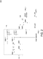
- Fig. 2 shows a circuit diagram for the power supply circuit 200 according to one embodiment of the application.
- the first DC-DC converter 110 for example, may be implemented by a buck-boost DC converter.
- the switch SW7 When the voltage source VBAT is not high enough, the switch SW7 is turned off and the switches SW1 and SW8 are toggled complementary based on the duty produced by the control component 150. On the contrary, when the voltage source VBAT is high enough, the switches SW1 is turned OFF and the switches SW7 and SW8 are toggled complementary based on the duty produced by the control component 150 to produce the desired DC voltage.
- the situation when the power supply circuit 200 is required to generate an APT output voltage VAPT1 and an ET output voltage VET1 is described as follows.
- the control component 150 which is not shown in Fig. 2 for simplicity
- the first DC-DC converter 110 it is arranged to receive an input voltage Vin from a battery or any other supply voltage provider to generate a stable output voltage Vout at an output node.
- the first DC-DC converter 110 (which may be a buck-boost converter) includes switches SW2, SW3, SW4, SW5_1-SW5_M and SW6_1-SW6_N, an inductor L, and capacitors C1_1-C1_N and C2_1-C2_M.
- M and N are the number of the outputs VHF and VAPT of the first DC-DC converter 110. Although in Fig. 2 , M and N are both 1 but the application is not limited by.
- the switch SW2 is coupled between the input voltage Vin and a first terminal N1 of the inductor L.
- the switch SW3 is coupled between the first terminal N1 of the inductor L and a reference voltage VSS (in this embodiment, the reference voltage is a ground voltage).
- the switches SW5_1 to SW5_M are coupled between a second terminal N2 of the inductor L and the respective one of the output voltages VHF1-VHFM.
- the switches SW6_1 to SW6_N are coupled between the second terminal N2 of the inductor L and the respective one of the output voltages VAPT1-VAPTN.
- the SW4 is coupled between the second terminal N2 of the inductor L and the reference voltage.
- the capacitors C1_1-C1_N are coupled between VSS and the respective one of the switch SW6_1-SW6_N and the capacitors C1_1-C1_N hold the APT output voltages VAPT1-VAPTN.
- the capacitors C2_1-C2_M are coupled between VSS and the respective one of the switch SW5_1-SW5_M, and the capacitors C2_1-C2_M hold the DC intermediate voltages VHF1-VHFM.
- the first DC-DC converter 110 may generate the output voltages higher or lower than the input voltage Vin.
- the control component 150 when the first DC-DC converter operates in the buck mode, the control component 150 generates the control signals to control the switches SW2 and SW3, respectively, to make the switches SW2 and SW3 to turn on and off alternately, and the switches SW2 and SW3 are not turned on simultaneously.
- the control component 150 further generates the control signals to turn on and turn off the switches SW5_1-SW5_M and SW6_1-SW6_N, and further generates the control signal to always turn off the switch SW4 for generating the proper step down output voltages.
- the first DC-DC converter 110 generates the APT output voltages VAPT1-VAPTN and the DC intermediate voltages VHF1-VHFM. Because the second DC-DC converter 120 is to be operated for generating output voltage, the DC intermediate voltage VHF1 from the first DC-DC converter 110 or the voltage source VBAT is used by the second DC-DC converter 120 via the switches SW1 or SW7, based on whether the voltage source VBAT is high enough or not.
- the second DC-DC converter 120 by switching the switches SW1 and SW8 or by switching the switches SW7 and SW8 according to the duty cycle signal generated from the control component 150, the second DC-DC converter 120 generates the M DC ET output voltage ET_DC1-ET_DCM.
- the linear amplifier 130_1-130_M produce the M AC ET voltages ET_AC1-ET_ACM.
- the second DC-DC converter 120 via the AC coupled capacitor, and by switching multiple output power transistors (for example, the power transistor 210_1 in Fig. 2 ) according to the output voltage acquired for DC voltage levels, the second DC-DC converter 120 generates M DC ET output voltages ET_DC1-ET_DC_M.
- the second DC-DC converter 120 further includes power transistors 210_1-210_M.
- power transistors 210_1-210_M In SIMO buck structure, multiple outputs voltages may be produced by switching inductor current into several paths. Each of the power transistors 210_1-210-M conducts inductor current for a fraction of the time to avoid short circuiting the outputs.
- the DC-DC converter charges and discharges the inductor from input to one of the M DC ET voltages ET_DC1-ET DCM at a time. In steady state, the average voltage across the inductor L2 is zero, by determining the ON duty of the switch SW7 (or the switch SW1 if in low battery state) and each of the power transistors 210_1-210_M. The ON duty of the switch SW7 (or the switch SW1 if in low battery state) will be the summation of the ON duty of the power transistors 210_1-210_M.
- the second DC-DC converter 120 may be also a SIMO circuit configuration for generating a plurality of different ET DC output voltages ET_DC1-ET_DC_M.
- Fig. 3 shows a circuit diagram for the power supply circuit 300 according to one embodiment of the application.
- the first DC-DC converter 110 for example, may be implemented by a SIMO buck-boost DC converter.
- the circuit configuration of the power supply circuit 300 is similar to that of the power supply circuit 200 of Fig. 2 and thus the details are omitted here.
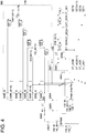
- Fig. 4 shows switching conditions of the switches of the power supply circuit 300 of Fig. 3 . Under control of the control component 150 (which is not shown in Fig. 3 and Fig.
- the switches SW2 and SW3 will toggle simultaneously according to the first duty control signal from the control component 150, to make the switches SW2 and SW3 to turn on and off alternately; and the switch SW4 and the rest of the switches SW5_1-SW5_M and SW6_1-SW6-N will toggle simultaneously according to multiple duty control signal related to each of the output voltage's condition, but each of the other switches will not turn on at the same time.
- the first DC-DC converter 110 generates the APT output voltages VAPT1-VAPTK and the DC intermediate voltages VHF(K+1)-VHFM. In other words, the first DC-DC converter 110 does not provide the APT output voltages VAPT(K+1)-VAPTN and the DC intermediate voltages VHF1-VHFK.
- the DC intermediate voltage VHF1 from the first DC-DC converter 110 or the voltage source VBAT is used by the second DC-DC converter 120 via the switches SW1 or SW7, based on whether the voltage source VBAT is high enough or not.
- the second DC-DC converter 120 by switching the switches SW1 and SW8 or by switching the switches SW7 and SW8 according to the duty cycle signal generated from the control component 150, and by switching multiple output switches according to the output voltage acquired for DC voltage levels, the second DC-DC converter 120 generates M DC ET output voltages ET_DC1-ET_DC_M.
- the linear amplifiers 130_(K+1)-130_M produce the AC ET voltage ET_AC(K+1)-ET_ACM, respectively. Because the first DC-DC converter 110 can generate the DC intermediate voltages VHF1-VHFK to support K APT mode voltages by turn on the bypass switches 140_1-140_M in M ET system, the linear amplifiers 130_1-130_K do not provide the AC ET voltages ET_AC1-ET_ACK.
- bypass switches 140_1-140_M are controlled to be ON while the bypass switches 140_(K+1)-140_M are controlled to be OFF for ET mode operation.
- the DC ET voltage ET_DC(K+1) is combined with the AC ET voltage ET_AC(K+1) from the linear amplifier 130_(K+1) into the ET output voltage VET(K+1); ... and via AC coupled or DC coupled paths, the DC ET voltage ET_DCM is combined with the AC ET voltage ET_ACM from the linear amplifier 130_M into the ET output voltage VETM.
- the ET output voltages VET1-VETK can generate APT power by the first DC-DC converter 110 via the bypass switches 140_1-140_K.
- the first DC-DC converter 110 may produce N APT output voltages VAPT1-VAPTN (N being a natural number).
- the power supply circuit may produce N APT output voltages VAPT1-VAPTN.
- the first DC-DC converter 110 may produce K (K being smaller than M) APT output voltages VAPT1-VAPTK by the bypass switches, the second DC-DC converter 120 may generate the (M-K) DC ET voltage ET_DC(K+1)-ET_DCM, and the linear amplifiers may generate (M-K) AC ET voltages ET_AC(K+1)-ET_ACM.
- the power supply circuit produce K APT output voltages VAPT1-VAPTK and produce (M-K) ET voltages VET(K+1)-VETM along with the N pure APT power.
- the power supply circuit of the above embodiments of the application may provide power to multiple ET PAs (power amplifiers) and/or multiple APT PAs with less cost and more flexibility because it is enough for the power supply circuit to use a few inductors (for example, 2 inductors in Fig. 2-Fig. 4 ) to provide multiple ET output voltages and/or multiple APT output voltages.
- ET PAs power amplifiers
- APT PAs APT PAs
- the application is directed to a wireless mobile device which includes the power supply circuit of the above embodiments of the application and a plurality of power amplification components.
- the plurality of power amplification components may include at least a first subset and a second subset.
- Each power amplification component of the first subset of the power amplification components is configured to operate according to an APT (average power tracking) mode.
- Each power amplification component of the second subset of the power amplification components is configured to operate according to an ET (envelop tracking) mode.
Landscapes
- Engineering & Computer Science (AREA)
- Power Engineering (AREA)
- Computer Networks & Wireless Communication (AREA)
- Signal Processing (AREA)
- Microelectronics & Electronic Packaging (AREA)
- Amplifiers (AREA)
Abstract
Description
- The disclosure relates in general to a power supply circuit for wireless mobile device having a plurality of multi-mode power amplification components.
- Wireless mobile devices (for example, smart phones) are increasingly required to operate in multiple modes, e.g. Global System for Mobile Communications (GSM), General Packet Radio Service (GPRS), code division multiple access (CDMA), wideband CDMA (WCDMA) and long term evolution (LTE). Wireless handsets are also increasingly required to operate in multiple frequency bands (e.g. 700, 800, 900, 1700, 1800, 1900, 2100, and 2600 MHz bands).
- Multi-mode and multi-band wireless mobile devices typically contain a plurality of power amplifiers (PA) for each individual mode and each individual operation band. For example, a quad-band GSM and tri-band WCDMA mobile device will often have one GSM power amplifier covering digital cellular service (DCS) and personal communications service (PCS) bands, one GSM power amplifier covering United States cellular and European cellular bands, one WCDMA power amplifier for United States cellular band, one WCDMA power amplifier for PCS band, and one WCDMA power amplifier for International Mobile Telecommunications-2000 (IMT-2000) band.
- Wireless mobile devices use dedicated power amplifier circuits for each band and each mode to optimize input and output matches to achieve the best linearity and/or efficiency for the given mode or band of operation. Some power amplifiers prefer ET (envelop tracking) for better efficiency while others prefer APT (average power tracking) for wider bandwidth.
- Therefore, there is a need in the art for an improved power supply circuit to supply power to multi-mode power amplifiers with less cost and more flexibility.
- According to one embodiment, provided is a power supply circuit for a wireless mobile device. The wireless mobile device includes a plurality of power amplification components, each power amplification component of a first subset of the power amplification components is configured to operate according to an APT (average power tracking) mode and each power amplification component of a second subset of the power amplification components is configured to operate according to either an ET (envelop tracking) mode or the APT mode. The power supply circuit includes: a first DC(direct current)-DC converter, coupled to the first subset of the power amplification components, the first DC-DC converter being configured to provide a plurality of APT output voltages and/or a plurality of DC intermediate voltages, the plurality of APT output voltages being provided to the first subset of the power amplification components, respectively; a second DC-DC converter, coupled to the first DC-DC converter and the second subset of the power amplification components, the second DC-DC converter being configured to provide a plurality of DC components of a plurality of ET output voltages; a plurality of linear amplifiers, coupled to the first DC-DC converter and the second subset of the power amplification components; and a plurality of bypass switches, coupled to the first DC-DC converter and the second subset of the power amplification components, for bypassing the plurality of DC intermediate voltages directly to the second subset of the power amplification components when the second subset of the power amplification components are to be operated under the APT mode. When the plurality of linear amplifiers receive the plurality of DC intermediate voltages from the first DC-DC converter, the plurality of linear amplifiers provide a plurality of AC components of the plurality of ET output voltages, respectively. The plurality of DC components of the plurality of ET output voltages and the plurality of AC components of the plurality of ET output voltages are combined into the plurality of ET output voltages, respectively and the plurality of ET output voltages are provided to the second subset of the power amplification components, respectively.
- According to another embodiment, provided is a power supply circuit for a wireless mobile device having a plurality of power amplification components. The power supply circuit includes: a first DC-DC converter, coupled to the power amplification components, the first DC-DC converter being configured to provide at least one constant output voltage and/or at least one DC intermediate voltage, the at least one constant output voltage being provided to the power amplification components; a second DC-DC converter, coupled to the first DC-DC converter and the power amplification components, the second DC-DC converter being configured to provide a DC component of at least one time-varying output voltage; and at least one linear amplifier, coupled to the first DC-DC converter and the power amplification components. When the at least one linear amplifier receives the at least one DC intermediate voltage from the first DC-DC converter, the at least one linear amplifier provides at least one AC component of the at least one time-varying output voltage. The DC component of the at least one time-varying output voltage and the at least one AC component of the at least one time-varying output voltage are combined into the at least one time-varying output voltage and provided to the power amplification components.
-
-
FIG. 1 shows a power supply circuit according to one embodiment of the application. -
Fig. 2 shows a circuit diagram for a power supply circuit according to one embodiment of the application. -
Fig. 3 shows a circuit diagram for a power supply circuit according to one embodiment of the application. -
Fig. 4 shows switching conditions of the switches of the power supply circuit ofFig. 3 . - In the following detailed description, for purposes of explanation, numerous specific details are set forth in order to provide a thorough understanding of the disclosed embodiments. It will be apparent, however, that one or more embodiments may be practiced without these specific details. In other instances, well-known structures and devices are schematically shown in order to simplify the drawing.
- Referring to
FIG. 1 , a power supply circuit according to one embodiment of the application is shown. Thepower supply circuit 100 includes a first DC (direct current)-DC converter 110, a second DC-DC converter 120, a plurality of linear amplifiers 130_1-130_M (M is a natural number and is larger than or equal to 1), bypass switches 140_1-140_M and acontrol component 150. Thepower supply circuit 100 further includes a switch SW1 to control whether the output from the first DC-DC converter 110 is allowed to be conducted to the second DC-DC converter 120. Thepower supply circuit 100 may provide power to power amplifiers 160_1-160_N (N is a natural number and is larger than or equal to 1) and 170_1-170_M. In other words, the power amplifiers 160_1-160_N and 170_1-170_M may include a first subset and a second subset, the first subset including the power amplifiers 160_1-160_N and the second subset including the power amplifiers 170_1-170_M. Each of the first subset of the power amplifiers 160_1-160_N is configured to operate according to an APT (average power tracking) mode. Each of the second subset of the power amplifiers 170_1-170_M can be configured to operate both according to ET (envelop tracking) mode or APT mode. - The first DC-
DC converter 110 may be configured to provide at least one APT output voltage (wherein the APT output voltage is a constant voltage) which may be provided to at least one of the first subset (i.e. the power amplifiers 160_1-160_N) of the power amplifiers. In more details, in one of the operation modes of the power supply circuit of the embodiment of the application, the first DC-DC converter 110 may be configured to provide N APT output voltages VAPT1-VAPTN to provide to N power amplifiers 160_1-160_N, respectively. The power supply circuit of the embodiment of the application may determine the APT output voltage based on system performance and the APT output voltage may be constant for a period of time. - The second DC-
DC converter 120 is coupled to the second subset (i.e. the power amplifiers 170_1-170_M) of the power amplifiers. When thepower supply circuit 100 is required to provide at least one ET output voltage (the ET output voltage may be a timing-varying voltage), the first DC-DC converter 110, the second DC-DC converter 120 and the linear amplifiers 130_1-130_M will be operated to provide the at least one ET output voltage. In more details, in another one of the operation modes of the power supply circuit of the embodiment of the application, the first DC-DC converter 110, the second DC-DC converter 120 and the linear amplifiers 130_1-130_M may operate to provide at most M ET output voltages VET1-VETM to provide to M power amplifiers 170_1-170_M which are operated in ET mode, respectively. The power supply circuit of the embodiment of the application may determine the ET output voltage based on output power of the ET PAs through a mapping function. - The first DC-
DC converter 110 provides a DC intermediate voltage VHF1 to the second DC-DC converter 120; and further the first DC-DC converter 110 provides DC intermediate voltages VHF1-VHFM to the linear amplifiers 130_1-130_M, respectively. Thus, the first DC-DC converter 110 may be a SIMO (single inductor multiple outputs) circuit configuration, and of course, the application is not limited by this. - The second DC-
DC converter 120 converts the DC intermediate voltage VHF1 from the first DC-DC converter 110 into M DC ET voltages ET_DC1-ET_DCM. - The linear amplifiers 130_1-130_M provide M AC ET voltages ET_AC1-ET_ACM, respectively. Details of the circuit configuration and operations of the linear amplifiers 130_1-130_M are not specified here.
- In details, M DC ET voltages ET_DC1-ET_DCM are combined with the respective one of the M AC ET voltages ET_AC1-ET_ACM into each of the M ET output voltages VET1-VETM, respectively. For example, the DC ET voltage ET_DC1 is combined with the AC ET voltage ET_AC1 from the linear amplifier 130_1 into the ET output voltage VET1; and the DC ET voltage ET_DCM is combined with the AC ET voltage ET_ACM from the linear amplifier 130_M into the ET output voltage VETM. The M DC ET voltages ET_DC1-ET_DCM are DC components of the ET output voltages VET1-VETM, respectively. The AC ET voltages ET_AC1-ET_ACM are AC components of the ET output voltages VET1-VETM, respectively.
- The
control component 150 is configured to control switch operations of the first DC-DC converter 110 and the second DC-DC converter 120. - The bypass switches 140_1-140_M are used to bypass the output voltages VHF1-VHFM directly from the first DC-
DC converter 110 to the power amplifiers 170_1-170_M, respectively if APT mode in the second subsets of PAs is needed. In other words, when any one of the power amplifiers 170_1-170_M is to be operated under APT mode, the corresponding linear amplifier will not operate and the second DC-DC converter 120 will not supply the corresponding DC ET voltage (ET_DC1-ET_DCM), while the corresponding one of the bypass switches 140_1-140_M will be in connection states to bypass the corresponding one of the voltages VHF1-VHFM directly from the first DC-DC converter 110 to the corresponding one of the power amplifiers 170_1-170_M, respectively. When any one of power amplifiers 170_1-170_M is to be operated under ET mode, the corresponding one of the bypass switches 140_1-140_M will be in disconnection states and the corresponding one of the voltages VHF1-VHFM from the first DC-DC converter 110 will be received by the linear amplifiers 130_1-130_M, respectively, to supply the linear amplifier to provide AC power ET_AC to the power amplifier while the DC power will be supply from one of the M DC ET voltages ET_DC1-ET_DCM from the second DC-DC converter 120. -
Fig. 2 shows a circuit diagram for thepower supply circuit 200 according to one embodiment of the application. As shown inFig. 2 , the first DC-DC converter 110, for example, may be implemented by a buck-boost DC converter. - When the voltage source VBAT is not high enough, the switch SW7 is turned off and the switches SW1 and SW8 are toggled complementary based on the duty produced by the
control component 150. On the contrary, when the voltage source VBAT is high enough, the switches SW1 is turned OFF and the switches SW7 and SW8 are toggled complementary based on the duty produced by thecontrol component 150 to produce the desired DC voltage. - The situation when the
power supply circuit 200 is required to generate an APT output voltage VAPT1 and an ET output voltage VET1 is described as follows. Under control of the control component 150 (which is not shown inFig. 2 for simplicity), in the first DC-DC converter 110, it is arranged to receive an input voltage Vin from a battery or any other supply voltage provider to generate a stable output voltage Vout at an output node. The first DC-DC converter 110 (which may be a buck-boost converter) includes switches SW2, SW3, SW4, SW5_1-SW5_M and SW6_1-SW6_N, an inductor L, and capacitors C1_1-C1_N and C2_1-C2_M. M and N are the number of the outputs VHF and VAPT of the first DC-DC converter 110. Although inFig. 2 , M and N are both 1 but the application is not limited by. The switch SW2 is coupled between the input voltage Vin and a first terminal N1 of the inductor L. The switch SW3 is coupled between the first terminal N1 of the inductor L and a reference voltage VSS (in this embodiment, the reference voltage is a ground voltage). The switches SW5_1 to SW5_M are coupled between a second terminal N2 of the inductor L and the respective one of the output voltages VHF1-VHFM. The switches SW6_1 to SW6_N are coupled between the second terminal N2 of the inductor L and the respective one of the output voltages VAPT1-VAPTN. The SW4 is coupled between the second terminal N2 of the inductor L and the reference voltage. The capacitors C1_1-C1_N are coupled between VSS and the respective one of the switch SW6_1-SW6_N and the capacitors C1_1-C1_N hold the APT output voltages VAPT1-VAPTN. The capacitors C2_1-C2_M are coupled between VSS and the respective one of the switch SW5_1-SW5_M, and the capacitors C2_1-C2_M hold the DC intermediate voltages VHF1-VHFM. - The first DC-
DC converter 110 may generate the output voltages higher or lower than the input voltage Vin. For example, when the first DC-DC converter operates in the buck mode, thecontrol component 150 generates the control signals to control the switches SW2 and SW3, respectively, to make the switches SW2 and SW3 to turn on and off alternately, and the switches SW2 and SW3 are not turned on simultaneously. Thecontrol component 150 further generates the control signals to turn on and turn off the switches SW5_1-SW5_M and SW6_1-SW6_N, and further generates the control signal to always turn off the switch SW4 for generating the proper step down output voltages. By this, the first DC-DC converter 110 generates the APT output voltages VAPT1-VAPTN and the DC intermediate voltages VHF1-VHFM. Because the second DC-DC converter 120 is to be operated for generating output voltage, the DC intermediate voltage VHF1 from the first DC-DC converter 110 or the voltage source VBAT is used by the second DC-DC converter 120 via the switches SW1 or SW7, based on whether the voltage source VBAT is high enough or not. - Also, in the second DC-
DC converter 120, by switching the switches SW1 and SW8 or by switching the switches SW7 and SW8 according to the duty cycle signal generated from thecontrol component 150, the second DC-DC converter 120 generates the M DC ET output voltage ET_DC1-ET_DCM. - The linear amplifier 130_1-130_M produce the M AC ET voltages ET_AC1-ET_ACM. Thus, via the AC coupled capacitor, and by switching multiple output power transistors (for example, the power transistor 210_1 in
Fig. 2 ) according to the output voltage acquired for DC voltage levels, the second DC-DC converter 120 generates M DC ET output voltages ET_DC1-ET_DC_M. - Also, in
Fig. 2 , the second DC-DC converter 120 further includes power transistors 210_1-210_M. In SIMO buck structure, multiple outputs voltages may be produced by switching inductor current into several paths. Each of the power transistors 210_1-210-M conducts inductor current for a fraction of the time to avoid short circuiting the outputs. The DC-DC converter charges and discharges the inductor from input to one of the M DC ET voltages ET_DC1-ET DCM at a time. In steady state, the average voltage across the inductor L2 is zero, by determining the ON duty of the switch SW7 (or the switch SW1 if in low battery state) and each of the power transistors 210_1-210_M. The ON duty of the switch SW7 (or the switch SW1 if in low battery state) will be the summation of the ON duty of the power transistors 210_1-210_M. - The second DC-
DC converter 120 may be also a SIMO circuit configuration for generating a plurality of different ET DC output voltages ET_DC1-ET_DC_M. -
Fig. 3 shows a circuit diagram for thepower supply circuit 300 according to one embodiment of the application. As shown inFig. 3 , the first DC-DC converter 110, for example, may be implemented by a SIMO buck-boost DC converter. The circuit configuration of thepower supply circuit 300 is similar to that of thepower supply circuit 200 ofFig. 2 and thus the details are omitted here. - The situation when the
power supply circuit 300 is required to generate K (K being a natural number and K≦M) APT output voltages VAPT1-VAPTK and (M-K) ET output voltages VET(K+1)-VETM is described as follows, with reference toFig. 4. Fig. 4 shows switching conditions of the switches of thepower supply circuit 300 ofFig. 3 . Under control of the control component 150 (which is not shown inFig. 3 andFig. 4 for simplicity), in the first DC-DC converter 110, the switches SW2 and SW3 will toggle simultaneously according to the first duty control signal from thecontrol component 150, to make the switches SW2 and SW3 to turn on and off alternately; and the switch SW4 and the rest of the switches SW5_1-SW5_M and SW6_1-SW6-N will toggle simultaneously according to multiple duty control signal related to each of the output voltage's condition, but each of the other switches will not turn on at the same time.. By this, the first DC-DC converter 110 generates the APT output voltages VAPT1-VAPTK and the DC intermediate voltages VHF(K+1)-VHFM. In other words, the first DC-DC converter 110 does not provide the APT output voltages VAPT(K+1)-VAPTN and the DC intermediate voltages VHF1-VHFK. - Because the second DC-
DC converter 120 is to be operated for generating output voltage, the DC intermediate voltage VHF1 from the first DC-DC converter 110 or the voltage source VBAT is used by the second DC-DC converter 120 via the switches SW1 or SW7, based on whether the voltage source VBAT is high enough or not. - Also, in the second DC-
DC converter 120, by switching the switches SW1 and SW8 or by switching the switches SW7 and SW8 according to the duty cycle signal generated from thecontrol component 150, and by switching multiple output switches according to the output voltage acquired for DC voltage levels, the second DC-DC converter 120 generates M DC ET output voltages ET_DC1-ET_DC_M. - The linear amplifiers 130_(K+1)-130_M produce the AC ET voltage ET_AC(K+1)-ET_ACM, respectively. Because the first DC-
DC converter 110 can generate the DC intermediate voltages VHF1-VHFK to support K APT mode voltages by turn on the bypass switches 140_1-140_M in M ET system, the linear amplifiers 130_1-130_K do not provide the AC ET voltages ET_AC1-ET_ACK. - Among the bypass switches 140_1-140_M, the bypass switches 140_1-140_K are controlled to be ON while the bypass switches 140_(K+1)-140_M are controlled to be OFF for ET mode operation.
- Thus, via the AC coupled or DC coupled paths, the DC ET voltage ET_DC(K+1) is combined with the AC ET voltage ET_AC(K+1) from the linear amplifier 130_(K+1) into the ET output voltage VET(K+1); ... and via AC coupled or DC coupled paths, the DC ET voltage ET_DCM is combined with the AC ET voltage ET_ACM from the linear amplifier 130_M into the ET output voltage VETM. The ET output voltages VET1-VETK can generate APT power by the first DC-
DC converter 110 via the bypass switches 140_1-140_K. - In brief, in the embodiments of the application, in one operation mode of the power supply circuit, the first DC-
DC converter 110 may produce N APT output voltages VAPT1-VAPTN (N being a natural number). In other words, the power supply circuit may produce N APT output voltages VAPT1-VAPTN. - In the embodiments of the application, in another operation mode of the power supply circuit, the first DC-
DC converter 110 may produce K (K being smaller than M) APT output voltages VAPT1-VAPTK by the bypass switches, the second DC-DC converter 120 may generate the (M-K) DC ET voltage ET_DC(K+1)-ET_DCM, and the linear amplifiers may generate (M-K) AC ET voltages ET_AC(K+1)-ET_ACM. In other words, the power supply circuit produce K APT output voltages VAPT1-VAPTK and produce (M-K) ET voltages VET(K+1)-VETM along with the N pure APT power. - The power supply circuit of the above embodiments of the application may provide power to multiple ET PAs (power amplifiers) and/or multiple APT PAs with less cost and more flexibility because it is enough for the power supply circuit to use a few inductors (for example, 2 inductors in
Fig. 2-Fig. 4 ) to provide multiple ET output voltages and/or multiple APT output voltages. - Another possible embodiment of the application is directed to a wireless mobile device which includes the power supply circuit of the above embodiments of the application and a plurality of power amplification components. The plurality of power amplification components may include at least a first subset and a second subset. Each power amplification component of the first subset of the power amplification components is configured to operate according to an APT (average power tracking) mode. Each power amplification component of the second subset of the power amplification components is configured to operate according to an ET (envelop tracking) mode.
Claims (14)
- A power supply circuit (100) for a wireless mobile device having a plurality of power amplification components (160_1-160_N, 170_1-170_M), wherein each power amplification component of a first subset (160_1-160_N) of the power amplification components is configured to operate according to an APT (average power tracking) mode and each power amplification component of a second subset (170_1-170_M) of the power amplification components is configured to operate according to either an ET (envelop tracking) mode or the APT mode, characterized in that the power supply circuit includes:a first DC(direct current)-DC converter (110), coupled to the first subset of the power amplification components, the first DC-DC converter being configured to provide a plurality of APT output voltages (VAPT1-VATPN) and/or a plurality of DC intermediate voltages (VHF1-VHFM), the plurality of APT output voltages being provided to the first subset of the power amplification components, respectively;a second DC-DC converter (120), coupled to the first DC-DC converter and the second subset of the power amplification components, the second DC-DC converter being configured to provide a plurality of DC components (ET_DC1-ET_DCM) of a plurality of ET output voltages (VET1-VETM);a plurality of linear amplifiers (130_1-130_M), coupled to the first DC-DC converter and the second subset of the power amplification components; anda plurality of bypass switches (140_1-140_M), coupled to the first DC-DC converter and the second subset of the power amplification components, for bypassing the plurality of DC intermediate voltages directly to the second subset of the power amplification components when the second subset of the power amplification components are to be operated under the APT mode,wherein when the plurality of linear amplifiers receive the plurality of DC intermediate voltages from the first DC-DC converter, the plurality of linear amplifiers provide a plurality of AC components (ET_AC1-ET_ACM) of the plurality of ET output voltages, respectively;wherein the plurality of DC components of the plurality of ET output voltages and the plurality of AC components of the plurality of ET output voltages are combined into the plurality of ET output voltages, respectively and the plurality of ET output voltages are provided to the second subset of the power amplification components, respectively.
- The power supply circuit according to claim 1, further includes:a control component (150), coupled to and for controlling the first DC-DC converter, the second DC-DC converter and the bypass switches.
- The power supply circuit according to claim 2, wherein:the second DC-DC converter is configured to provide the plurality of DC components of the plurality of ET output voltages based on the plurality of DC intermediate voltages or based on a voltage source.
- The power supply circuit according to claim 3, further includes:a first switch (SW1), coupled between one output of the first DC-DC converter and a first terminal of an inductor (L2) of the second DC-DC converter, the first switch being controlled by the control component for conducting one of the voltage source and the one of the plurality of DC intermediate voltages into the second DC-DC converter.
- The power supply circuit according to claim 1, whereinthe first DC-DC converter provides the N APT output voltages to the N power amplification components of the first subset of the power amplification components, respectively, N being a natural number; andthe first DC-DC converter provides none of the plurality of DC intermediate voltages to the plurality of linear amplifiers.
- The power supply circuit according to claim 1, whereinthe first DC-DC converter provides the K APT output voltages to the second subset of the power amplification components by the bypass switches, respectively,the first DC-DC converter provides the M-K DC intermediate voltages to the M-K linear amplifiers, respectively,the M-K linear amplifiers provide the M-KAC components of the plurality of ET output voltages, respectively,the plurality of DC components of the plurality of ET output voltages and the M-K AC components of the plurality of ET output voltages are combined into the M-K ET output voltages and provided to the second subset of the power amplification components, respectively, andM and K are natural number, and K is smaller than or equal to M.
- The power supply circuit according to claim 1, whereinthe first DC-DC converter is a SIMO (single inductor multiple output) circuit configuration which includes a single first inductor (L1).
- The power supply circuit according to claim 1, whereinthe second DC-DC converter is a SIMO (single inductor multiple output) circuit configuration which includes a single second inductor (L2).
- A power supply circuit (100) for a wireless mobile device having a plurality of power amplification components (160_1-160_N, 170_1-170_M), characterized in that the power supply circuit includes:a first DC-DC converter (110), coupled to the power amplification components, the first DC-DC converter being configured to provide at least one constant output voltage and/or at least one DC intermediate voltage, the at least one constant output voltage being provided to the power amplification components;a second DC-DC converter (120), coupled to the first DC-DC converter and the power amplification components, the second DC-DC converter being configured to provide a DC component of at least one time-varying output voltage; andat least one linear amplifier (130_1-130_M), coupled to the first DC-DC converter and the power amplification components,wherein when the at least one linear amplifier receives the at least one DC intermediate voltage from the first DC-DC converter, the at least one linear amplifier provides at least one AC component of the at least one time-varying output voltage;wherein the DC component of the at least one time-varying output voltage and the at least one AC component of the at least one time-varying output voltage are combined into the at least one time-varying output voltage and provided to the power amplification components.
- The power supply circuit according to claim 9, further includes:at least one bypass switch (140_1-140_M), coupled to the first DC-DC converter and a second subset (170_1-170_M) of the power amplification components, for bypassing the DC component of the at least one time-varying output voltage directly to the second subset of the power amplification components when the second subset of the power amplification components are to be operated under an APT (average power tracking) mode; anda control component (150), coupled to and for controlling the first DC-DC converter, the second DC-DC converter and the at least one bypass switch.
- The power supply circuit according to claim 10, wherein:the second DC-DC converter is configured to provide the DC component of at least one time-varying output voltage based on the at least one DC intermediate voltage or based on a voltage source.
- The power supply circuit according to claim 11, further includes:a first switch (SW1), coupled between one output of the first DC-DC converter and a first terminal (L2) of an inductor of the second DC-DC converter, the first switch being controlled by the control component for conducting one of the voltage source and the DC component of at least one time-varying output voltage into the second DC-DC converter.
- The power supply circuit according to claim 9, whereinthe first DC-DC converter is a SIMO (single inductor multiple output) circuit configuration which includes a single first inductor (L1).
- The power supply circuit according to claim 9, whereinthe second DC-DC converter is a SIMO (single inductor multiple output) circuit configuration which includes a single second inductor (L2).
Applications Claiming Priority (2)
| Application Number | Priority Date | Filing Date | Title |
|---|---|---|---|
| US201662374035P | 2016-08-12 | 2016-08-12 | |
| US15/492,013 US9912306B1 (en) | 2016-08-12 | 2017-04-20 | Power supply circuit of wireless mobile device |
Publications (2)
| Publication Number | Publication Date |
|---|---|
| EP3282579A1 true EP3282579A1 (en) | 2018-02-14 |
| EP3282579B1 EP3282579B1 (en) | 2019-08-07 |
Family
ID=59030818
Family Applications (1)
| Application Number | Title | Priority Date | Filing Date |
|---|---|---|---|
| EP17174786.8A Active EP3282579B1 (en) | 2016-08-12 | 2017-06-07 | Power supply circuit of wireless mobile device |
Country Status (4)
| Country | Link |
|---|---|
| US (1) | US9912306B1 (en) |
| EP (1) | EP3282579B1 (en) |
| CN (1) | CN107733461A (en) |
| TW (1) | TWI638514B (en) |
Cited By (2)
| Publication number | Priority date | Publication date | Assignee | Title |
|---|---|---|---|---|
| DE102018110784A1 (en) * | 2018-05-04 | 2019-11-07 | Abb Schweiz Ag | Autonomous wireless sensor device with reduced power consumption |
| DE102018110786A1 (en) * | 2018-05-04 | 2019-11-07 | Abb Schweiz Ag | Autonomous wireless sensor device |
Families Citing this family (9)
| Publication number | Priority date | Publication date | Assignee | Title |
|---|---|---|---|---|
| US11239755B2 (en) * | 2017-05-30 | 2022-02-01 | Skyworks Solutions, Inc. | Power management systems including a plurality of converters for providing dual integrated multi-mode power management |
| TWI644193B (en) * | 2017-10-20 | 2018-12-11 | 群光電能科技股份有限公司 | Multi-output control system |
| US11581854B2 (en) * | 2018-04-26 | 2023-02-14 | Mediatek Inc. | Envelope tracking supply modulator topology for wipe-bandwidth radio frequency transmitter |
| US11088660B2 (en) * | 2019-01-25 | 2021-08-10 | Mediatek Inc. | Power supply with envelope tracking modulation |
| WO2021062685A1 (en) * | 2019-09-30 | 2021-04-08 | 华为技术有限公司 | Envelope tracking modulator and transmitting device |
| CN110943700B (en) * | 2019-12-17 | 2023-04-18 | 北京紫光展锐通信技术有限公司 | Signal generation system and terminal device |
| US11677356B2 (en) | 2020-02-19 | 2023-06-13 | Samsung Electronics Co., Ltd. | Supply modulator and wireless communication apparatus including the same |
| US11909435B2 (en) * | 2020-11-02 | 2024-02-20 | Samsung Electronics Co., Ltd. | Method for multi-band communication and electronic device thereof |
| US12381522B2 (en) * | 2021-03-09 | 2025-08-05 | Skyworks Solutions, Inc. | Average power tracking systems with fast transient settling |
Citations (6)
| Publication number | Priority date | Publication date | Assignee | Title |
|---|---|---|---|---|
| US20130141068A1 (en) * | 2011-12-01 | 2013-06-06 | Rf Micro Devices, Inc. | Average power tracking controller |
| US20140266462A1 (en) * | 2013-03-14 | 2014-09-18 | Motorola Mobility Llc | Low power consumption adaptive power amplifier |
| US20140273897A1 (en) * | 2013-03-14 | 2014-09-18 | Quantance, Inc. | Power Supply |
| JP2014187432A (en) * | 2013-03-21 | 2014-10-02 | Sharp Corp | Communication signal amplifying circuit and control method for communication signal amplifying circuit |
| US20160065139A1 (en) * | 2014-09-02 | 2016-03-03 | Samsung Electronics Co., Ltd. | Method and apparatus for supplying power to a radio frequency power amplifier |
| US20160173031A1 (en) * | 2014-12-12 | 2016-06-16 | Intel Corporation | Envelope Tracking in Connection with Simultaneous Transmission in one or more Frequency Bands |
Family Cites Families (11)
| Publication number | Priority date | Publication date | Assignee | Title |
|---|---|---|---|---|
| JP3838547B2 (en) * | 2001-12-11 | 2006-10-25 | 株式会社ルネサステクノロジ | Power supply device for high frequency power amplifier circuit |
| WO2006111891A1 (en) * | 2005-04-20 | 2006-10-26 | Nxp B.V. | A power supply system. |
| KR100765790B1 (en) * | 2006-06-30 | 2007-10-12 | 삼성전자주식회사 | Variable power supply and method for mobile devices |
| GB2479182B (en) * | 2010-03-31 | 2015-04-01 | Sony Europe Ltd | Power amplifier |
| JP2011259083A (en) * | 2010-06-07 | 2011-12-22 | Renesas Electronics Corp | Rf power amplifier and operation method thereof |
| US9276428B2 (en) * | 2011-07-06 | 2016-03-01 | Htc Corporation | System power integrated circuit and architecture, management circuit, power supply arrangement, and portable apparatus |
| US8958762B2 (en) * | 2012-03-08 | 2015-02-17 | Htc Corporation | Apparatus and method for power management |
| US8737940B1 (en) * | 2013-02-28 | 2014-05-27 | Intel Mobile Communications GmbH | Envelope tracking system and method for calibrating a supply voltage of an envelope tracking power amplifier |
| US9319495B2 (en) * | 2013-08-06 | 2016-04-19 | Aura Semiconductor Pvt. Ltd | Power amplifier providing high efficiency |
| US9065509B1 (en) * | 2014-01-09 | 2015-06-23 | Mediatek Inc. | Methods and apparatus for envelope tracking system |
| US9991856B2 (en) * | 2014-09-25 | 2018-06-05 | Skyworks Solutions, Inc. | Variable load power amplifier supporting dual-mode envelope tracking and average power tracking performance |
-
2017
- 2017-04-20 US US15/492,013 patent/US9912306B1/en not_active Expired - Fee Related
- 2017-06-07 EP EP17174786.8A patent/EP3282579B1/en active Active
- 2017-06-20 TW TW106120528A patent/TWI638514B/en active
- 2017-06-28 CN CN201710504513.XA patent/CN107733461A/en not_active Withdrawn
Patent Citations (6)
| Publication number | Priority date | Publication date | Assignee | Title |
|---|---|---|---|---|
| US20130141068A1 (en) * | 2011-12-01 | 2013-06-06 | Rf Micro Devices, Inc. | Average power tracking controller |
| US20140266462A1 (en) * | 2013-03-14 | 2014-09-18 | Motorola Mobility Llc | Low power consumption adaptive power amplifier |
| US20140273897A1 (en) * | 2013-03-14 | 2014-09-18 | Quantance, Inc. | Power Supply |
| JP2014187432A (en) * | 2013-03-21 | 2014-10-02 | Sharp Corp | Communication signal amplifying circuit and control method for communication signal amplifying circuit |
| US20160065139A1 (en) * | 2014-09-02 | 2016-03-03 | Samsung Electronics Co., Ltd. | Method and apparatus for supplying power to a radio frequency power amplifier |
| US20160173031A1 (en) * | 2014-12-12 | 2016-06-16 | Intel Corporation | Envelope Tracking in Connection with Simultaneous Transmission in one or more Frequency Bands |
Cited By (2)
| Publication number | Priority date | Publication date | Assignee | Title |
|---|---|---|---|---|
| DE102018110784A1 (en) * | 2018-05-04 | 2019-11-07 | Abb Schweiz Ag | Autonomous wireless sensor device with reduced power consumption |
| DE102018110786A1 (en) * | 2018-05-04 | 2019-11-07 | Abb Schweiz Ag | Autonomous wireless sensor device |
Also Published As
| Publication number | Publication date |
|---|---|
| TWI638514B (en) | 2018-10-11 |
| US20180048272A1 (en) | 2018-02-15 |
| TW201806311A (en) | 2018-02-16 |
| US9912306B1 (en) | 2018-03-06 |
| EP3282579B1 (en) | 2019-08-07 |
| CN107733461A (en) | 2018-02-23 |
Similar Documents
| Publication | Publication Date | Title |
|---|---|---|
| US9912306B1 (en) | Power supply circuit of wireless mobile device | |
| US10985654B2 (en) | Switching regulator and method of operating the same | |
| US20250053186A1 (en) | Devices and methods related to voltage supply system with boost converter and charge pump | |
| KR102704900B1 (en) | Switching regulator for dynamically changing output voltage and power supply circuit including the same | |
| US11258359B2 (en) | Switching regulator generating continuous output delivery current and operating method thereof | |
| US11251708B2 (en) | Inverting switching regulator using charge pump and operating method thereof | |
| US20200228006A1 (en) | Devices and methods related to dual output charge pump | |
| US8159091B2 (en) | Switch circuit of DC/DC converter configured to conduct various modes for charging/discharging | |
| US8089253B2 (en) | Power supplies for RF power amplifier | |
| US7132891B1 (en) | Power amplifier control using a switching power supply | |
| US12191766B2 (en) | Hybrid power converter | |
| US20100264991A1 (en) | Switched capacitor voltage converter for a power amplifier | |
| US9413362B2 (en) | Differential charge pump | |
| US10840810B2 (en) | Devices and methods related to boost supply for low battery 2G bias support | |
| CN106558988A (en) | Shared integrated DC-DC source actuator | |
| KR20020028844A (en) | Dc/dc converter | |
| WO2017156638A1 (en) | Low-volume hybrid step-down dc-dc converter | |
| JP2014039109A (en) | Power amplifier and transmitter | |
| CN118214275A (en) | Switched capacitor conversion circuit and power supply equipment | |
| CN116941181A (en) | Power supply circuit for power amplifier and communication device | |
| US7683584B2 (en) | Power source switching apparatus and method thereof | |
| US20250023463A1 (en) | Multi-voltage power management integrated circuit | |
| CN215646222U (en) | Power management circuit, earphone charging box and wireless earphone system | |
| CN119966016A (en) | Power supply circuits and electronic equipment |
Legal Events
| Date | Code | Title | Description |
|---|---|---|---|
| PUAI | Public reference made under article 153(3) epc to a published international application that has entered the european phase |
Free format text: ORIGINAL CODE: 0009012 |
|
| STAA | Information on the status of an ep patent application or granted ep patent |
Free format text: STATUS: REQUEST FOR EXAMINATION WAS MADE |
|
| 17P | Request for examination filed |
Effective date: 20170607 |
|
| AK | Designated contracting states |
Kind code of ref document: A1 Designated state(s): AL AT BE BG CH CY CZ DE DK EE ES FI FR GB GR HR HU IE IS IT LI LT LU LV MC MK MT NL NO PL PT RO RS SE SI SK SM TR |
|
| AX | Request for extension of the european patent |
Extension state: BA ME |
|
| RBV | Designated contracting states (corrected) |
Designated state(s): AL AT BE BG CH CY CZ DE DK EE ES FI FR GB GR HR HU IE IS IT LI LT LU LV MC MK MT NL NO PL PT RO RS SE SI SK SM TR |
|
| STAA | Information on the status of an ep patent application or granted ep patent |
Free format text: STATUS: EXAMINATION IS IN PROGRESS |
|
| 17Q | First examination report despatched |
Effective date: 20180831 |
|
| GRAP | Despatch of communication of intention to grant a patent |
Free format text: ORIGINAL CODE: EPIDOSNIGR1 |
|
| STAA | Information on the status of an ep patent application or granted ep patent |
Free format text: STATUS: GRANT OF PATENT IS INTENDED |
|
| INTG | Intention to grant announced |
Effective date: 20190322 |
|
| GRAS | Grant fee paid |
Free format text: ORIGINAL CODE: EPIDOSNIGR3 |
|
| GRAA | (expected) grant |
Free format text: ORIGINAL CODE: 0009210 |
|
| STAA | Information on the status of an ep patent application or granted ep patent |
Free format text: STATUS: THE PATENT HAS BEEN GRANTED |
|
| AK | Designated contracting states |
Kind code of ref document: B1 Designated state(s): AL AT BE BG CH CY CZ DE DK EE ES FI FR GB GR HR HU IE IS IT LI LT LU LV MC MK MT NL NO PL PT RO RS SE SI SK SM TR |
|
| REG | Reference to a national code |
Ref country code: GB Ref legal event code: FG4D |
|
| REG | Reference to a national code |
Ref country code: CH Ref legal event code: EP Ref country code: AT Ref legal event code: REF Ref document number: 1165366 Country of ref document: AT Kind code of ref document: T Effective date: 20190815 |
|
| REG | Reference to a national code |
Ref country code: DE Ref legal event code: R096 Ref document number: 602017005829 Country of ref document: DE |
|
| REG | Reference to a national code |
Ref country code: IE Ref legal event code: FG4D |
|
| REG | Reference to a national code |
Ref country code: NL Ref legal event code: MP Effective date: 20190807 |
|
| REG | Reference to a national code |
Ref country code: LT Ref legal event code: MG4D |
|
| PG25 | Lapsed in a contracting state [announced via postgrant information from national office to epo] |
Ref country code: NO Free format text: LAPSE BECAUSE OF FAILURE TO SUBMIT A TRANSLATION OF THE DESCRIPTION OR TO PAY THE FEE WITHIN THE PRESCRIBED TIME-LIMIT Effective date: 20191107 Ref country code: BG Free format text: LAPSE BECAUSE OF FAILURE TO SUBMIT A TRANSLATION OF THE DESCRIPTION OR TO PAY THE FEE WITHIN THE PRESCRIBED TIME-LIMIT Effective date: 20191107 Ref country code: NL Free format text: LAPSE BECAUSE OF FAILURE TO SUBMIT A TRANSLATION OF THE DESCRIPTION OR TO PAY THE FEE WITHIN THE PRESCRIBED TIME-LIMIT Effective date: 20190807 Ref country code: SE Free format text: LAPSE BECAUSE OF FAILURE TO SUBMIT A TRANSLATION OF THE DESCRIPTION OR TO PAY THE FEE WITHIN THE PRESCRIBED TIME-LIMIT Effective date: 20190807 Ref country code: LT Free format text: LAPSE BECAUSE OF FAILURE TO SUBMIT A TRANSLATION OF THE DESCRIPTION OR TO PAY THE FEE WITHIN THE PRESCRIBED TIME-LIMIT Effective date: 20190807 Ref country code: HR Free format text: LAPSE BECAUSE OF FAILURE TO SUBMIT A TRANSLATION OF THE DESCRIPTION OR TO PAY THE FEE WITHIN THE PRESCRIBED TIME-LIMIT Effective date: 20190807 Ref country code: PT Free format text: LAPSE BECAUSE OF FAILURE TO SUBMIT A TRANSLATION OF THE DESCRIPTION OR TO PAY THE FEE WITHIN THE PRESCRIBED TIME-LIMIT Effective date: 20191209 Ref country code: FI Free format text: LAPSE BECAUSE OF FAILURE TO SUBMIT A TRANSLATION OF THE DESCRIPTION OR TO PAY THE FEE WITHIN THE PRESCRIBED TIME-LIMIT Effective date: 20190807 |
|
| REG | Reference to a national code |
Ref country code: AT Ref legal event code: MK05 Ref document number: 1165366 Country of ref document: AT Kind code of ref document: T Effective date: 20190807 |
|
| PG25 | Lapsed in a contracting state [announced via postgrant information from national office to epo] |
Ref country code: GR Free format text: LAPSE BECAUSE OF FAILURE TO SUBMIT A TRANSLATION OF THE DESCRIPTION OR TO PAY THE FEE WITHIN THE PRESCRIBED TIME-LIMIT Effective date: 20191108 Ref country code: ES Free format text: LAPSE BECAUSE OF FAILURE TO SUBMIT A TRANSLATION OF THE DESCRIPTION OR TO PAY THE FEE WITHIN THE PRESCRIBED TIME-LIMIT Effective date: 20190807 Ref country code: IS Free format text: LAPSE BECAUSE OF FAILURE TO SUBMIT A TRANSLATION OF THE DESCRIPTION OR TO PAY THE FEE WITHIN THE PRESCRIBED TIME-LIMIT Effective date: 20191207 Ref country code: RS Free format text: LAPSE BECAUSE OF FAILURE TO SUBMIT A TRANSLATION OF THE DESCRIPTION OR TO PAY THE FEE WITHIN THE PRESCRIBED TIME-LIMIT Effective date: 20190807 Ref country code: LV Free format text: LAPSE BECAUSE OF FAILURE TO SUBMIT A TRANSLATION OF THE DESCRIPTION OR TO PAY THE FEE WITHIN THE PRESCRIBED TIME-LIMIT Effective date: 20190807 Ref country code: AL Free format text: LAPSE BECAUSE OF FAILURE TO SUBMIT A TRANSLATION OF THE DESCRIPTION OR TO PAY THE FEE WITHIN THE PRESCRIBED TIME-LIMIT Effective date: 20190807 |
|
| PG25 | Lapsed in a contracting state [announced via postgrant information from national office to epo] |
Ref country code: TR Free format text: LAPSE BECAUSE OF FAILURE TO SUBMIT A TRANSLATION OF THE DESCRIPTION OR TO PAY THE FEE WITHIN THE PRESCRIBED TIME-LIMIT Effective date: 20190807 |
|
| PG25 | Lapsed in a contracting state [announced via postgrant information from national office to epo] |
Ref country code: AT Free format text: LAPSE BECAUSE OF FAILURE TO SUBMIT A TRANSLATION OF THE DESCRIPTION OR TO PAY THE FEE WITHIN THE PRESCRIBED TIME-LIMIT Effective date: 20190807 Ref country code: DK Free format text: LAPSE BECAUSE OF FAILURE TO SUBMIT A TRANSLATION OF THE DESCRIPTION OR TO PAY THE FEE WITHIN THE PRESCRIBED TIME-LIMIT Effective date: 20190807 Ref country code: IT Free format text: LAPSE BECAUSE OF FAILURE TO SUBMIT A TRANSLATION OF THE DESCRIPTION OR TO PAY THE FEE WITHIN THE PRESCRIBED TIME-LIMIT Effective date: 20190807 Ref country code: RO Free format text: LAPSE BECAUSE OF FAILURE TO SUBMIT A TRANSLATION OF THE DESCRIPTION OR TO PAY THE FEE WITHIN THE PRESCRIBED TIME-LIMIT Effective date: 20190807 Ref country code: EE Free format text: LAPSE BECAUSE OF FAILURE TO SUBMIT A TRANSLATION OF THE DESCRIPTION OR TO PAY THE FEE WITHIN THE PRESCRIBED TIME-LIMIT Effective date: 20190807 Ref country code: PL Free format text: LAPSE BECAUSE OF FAILURE TO SUBMIT A TRANSLATION OF THE DESCRIPTION OR TO PAY THE FEE WITHIN THE PRESCRIBED TIME-LIMIT Effective date: 20190807 |
|
| PG25 | Lapsed in a contracting state [announced via postgrant information from national office to epo] |
Ref country code: SK Free format text: LAPSE BECAUSE OF FAILURE TO SUBMIT A TRANSLATION OF THE DESCRIPTION OR TO PAY THE FEE WITHIN THE PRESCRIBED TIME-LIMIT Effective date: 20190807 Ref country code: SM Free format text: LAPSE BECAUSE OF FAILURE TO SUBMIT A TRANSLATION OF THE DESCRIPTION OR TO PAY THE FEE WITHIN THE PRESCRIBED TIME-LIMIT Effective date: 20190807 Ref country code: IS Free format text: LAPSE BECAUSE OF FAILURE TO SUBMIT A TRANSLATION OF THE DESCRIPTION OR TO PAY THE FEE WITHIN THE PRESCRIBED TIME-LIMIT Effective date: 20200224 Ref country code: CZ Free format text: LAPSE BECAUSE OF FAILURE TO SUBMIT A TRANSLATION OF THE DESCRIPTION OR TO PAY THE FEE WITHIN THE PRESCRIBED TIME-LIMIT Effective date: 20190807 |
|
| REG | Reference to a national code |
Ref country code: DE Ref legal event code: R097 Ref document number: 602017005829 Country of ref document: DE |
|
| PLBE | No opposition filed within time limit |
Free format text: ORIGINAL CODE: 0009261 |
|
| STAA | Information on the status of an ep patent application or granted ep patent |
Free format text: STATUS: NO OPPOSITION FILED WITHIN TIME LIMIT |
|
| PG2D | Information on lapse in contracting state deleted |
Ref country code: IS |
|
| 26N | No opposition filed |
Effective date: 20200603 |
|
| PG25 | Lapsed in a contracting state [announced via postgrant information from national office to epo] |
Ref country code: SI Free format text: LAPSE BECAUSE OF FAILURE TO SUBMIT A TRANSLATION OF THE DESCRIPTION OR TO PAY THE FEE WITHIN THE PRESCRIBED TIME-LIMIT Effective date: 20190807 |
|
| PG25 | Lapsed in a contracting state [announced via postgrant information from national office to epo] |
Ref country code: MC Free format text: LAPSE BECAUSE OF FAILURE TO SUBMIT A TRANSLATION OF THE DESCRIPTION OR TO PAY THE FEE WITHIN THE PRESCRIBED TIME-LIMIT Effective date: 20190807 |
|
| REG | Reference to a national code |
Ref country code: CH Ref legal event code: PL |
|
| PG25 | Lapsed in a contracting state [announced via postgrant information from national office to epo] |
Ref country code: LU Free format text: LAPSE BECAUSE OF NON-PAYMENT OF DUE FEES Effective date: 20200607 |
|
| REG | Reference to a national code |
Ref country code: BE Ref legal event code: MM Effective date: 20200630 |
|
| PG25 | Lapsed in a contracting state [announced via postgrant information from national office to epo] |
Ref country code: IE Free format text: LAPSE BECAUSE OF NON-PAYMENT OF DUE FEES Effective date: 20200607 Ref country code: CH Free format text: LAPSE BECAUSE OF NON-PAYMENT OF DUE FEES Effective date: 20200630 Ref country code: LI Free format text: LAPSE BECAUSE OF NON-PAYMENT OF DUE FEES Effective date: 20200630 |
|
| PG25 | Lapsed in a contracting state [announced via postgrant information from national office to epo] |
Ref country code: BE Free format text: LAPSE BECAUSE OF NON-PAYMENT OF DUE FEES Effective date: 20200630 |
|
| PG25 | Lapsed in a contracting state [announced via postgrant information from national office to epo] |
Ref country code: MT Free format text: LAPSE BECAUSE OF FAILURE TO SUBMIT A TRANSLATION OF THE DESCRIPTION OR TO PAY THE FEE WITHIN THE PRESCRIBED TIME-LIMIT Effective date: 20190807 Ref country code: CY Free format text: LAPSE BECAUSE OF FAILURE TO SUBMIT A TRANSLATION OF THE DESCRIPTION OR TO PAY THE FEE WITHIN THE PRESCRIBED TIME-LIMIT Effective date: 20190807 |
|
| PG25 | Lapsed in a contracting state [announced via postgrant information from national office to epo] |
Ref country code: MK Free format text: LAPSE BECAUSE OF FAILURE TO SUBMIT A TRANSLATION OF THE DESCRIPTION OR TO PAY THE FEE WITHIN THE PRESCRIBED TIME-LIMIT Effective date: 20190807 |
|
| P01 | Opt-out of the competence of the unified patent court (upc) registered |
Effective date: 20230607 |
|
| PGFP | Annual fee paid to national office [announced via postgrant information from national office to epo] |
Ref country code: GB Payment date: 20240627 Year of fee payment: 8 |
|
| PGFP | Annual fee paid to national office [announced via postgrant information from national office to epo] |
Ref country code: DE Payment date: 20240627 Year of fee payment: 8 |
|
| PGFP | Annual fee paid to national office [announced via postgrant information from national office to epo] |
Ref country code: FR Payment date: 20240625 Year of fee payment: 8 |
|
| REG | Reference to a national code |
Ref country code: DE Ref legal event code: R119 Ref document number: 602017005829 Country of ref document: DE |
|
| GBPC | Gb: european patent ceased through non-payment of renewal fee |
Effective date: 20250607 |
|
| PG25 | Lapsed in a contracting state [announced via postgrant information from national office to epo] |
Ref country code: GB Free format text: LAPSE BECAUSE OF NON-PAYMENT OF DUE FEES Effective date: 20250607 |
|
| PG25 | Lapsed in a contracting state [announced via postgrant information from national office to epo] |
Ref country code: DE Free format text: LAPSE BECAUSE OF NON-PAYMENT OF DUE FEES Effective date: 20260101 |
|
| PG25 | Lapsed in a contracting state [announced via postgrant information from national office to epo] |
Ref country code: FR Free format text: LAPSE BECAUSE OF NON-PAYMENT OF DUE FEES Effective date: 20250630 |