EP3282453A1 - Improved processing of polymer based inks and pastes - Google Patents
Improved processing of polymer based inks and pastes Download PDFInfo
- Publication number
- EP3282453A1 EP3282453A1 EP16183752.1A EP16183752A EP3282453A1 EP 3282453 A1 EP3282453 A1 EP 3282453A1 EP 16183752 A EP16183752 A EP 16183752A EP 3282453 A1 EP3282453 A1 EP 3282453A1
- Authority
- EP
- European Patent Office
- Prior art keywords
- electrically conductive
- substrate
- process according
- composition
- conductive composition
- Prior art date
- Legal status (The legal status is an assumption and is not a legal conclusion. Google has not performed a legal analysis and makes no representation as to the accuracy of the status listed.)
- Granted
Links
Images


Classifications
-
- H—ELECTRICITY
- H01—ELECTRIC ELEMENTS
- H01B—CABLES; CONDUCTORS; INSULATORS; SELECTION OF MATERIALS FOR THEIR CONDUCTIVE, INSULATING OR DIELECTRIC PROPERTIES
- H01B5/00—Non-insulated conductors or conductive bodies characterised by their form
- H01B5/14—Non-insulated conductors or conductive bodies characterised by their form comprising conductive layers or films on insulating-supports
-
- C—CHEMISTRY; METALLURGY
- C09—DYES; PAINTS; POLISHES; NATURAL RESINS; ADHESIVES; COMPOSITIONS NOT OTHERWISE PROVIDED FOR; APPLICATIONS OF MATERIALS NOT OTHERWISE PROVIDED FOR
- C09D—COATING COMPOSITIONS, e.g. PAINTS, VARNISHES OR LACQUERS; FILLING PASTES; CHEMICAL PAINT OR INK REMOVERS; INKS; CORRECTING FLUIDS; WOODSTAINS; PASTES OR SOLIDS FOR COLOURING OR PRINTING; USE OF MATERIALS THEREFOR
- C09D11/00—Inks
- C09D11/02—Printing inks
- C09D11/03—Printing inks characterised by features other than the chemical nature of the binder
- C09D11/033—Printing inks characterised by features other than the chemical nature of the binder characterised by the solvent
-
- C—CHEMISTRY; METALLURGY
- C09—DYES; PAINTS; POLISHES; NATURAL RESINS; ADHESIVES; COMPOSITIONS NOT OTHERWISE PROVIDED FOR; APPLICATIONS OF MATERIALS NOT OTHERWISE PROVIDED FOR
- C09D—COATING COMPOSITIONS, e.g. PAINTS, VARNISHES OR LACQUERS; FILLING PASTES; CHEMICAL PAINT OR INK REMOVERS; INKS; CORRECTING FLUIDS; WOODSTAINS; PASTES OR SOLIDS FOR COLOURING OR PRINTING; USE OF MATERIALS THEREFOR
- C09D11/00—Inks
- C09D11/02—Printing inks
- C09D11/03—Printing inks characterised by features other than the chemical nature of the binder
- C09D11/037—Printing inks characterised by features other than the chemical nature of the binder characterised by the pigment
-
- C—CHEMISTRY; METALLURGY
- C09—DYES; PAINTS; POLISHES; NATURAL RESINS; ADHESIVES; COMPOSITIONS NOT OTHERWISE PROVIDED FOR; APPLICATIONS OF MATERIALS NOT OTHERWISE PROVIDED FOR
- C09D—COATING COMPOSITIONS, e.g. PAINTS, VARNISHES OR LACQUERS; FILLING PASTES; CHEMICAL PAINT OR INK REMOVERS; INKS; CORRECTING FLUIDS; WOODSTAINS; PASTES OR SOLIDS FOR COLOURING OR PRINTING; USE OF MATERIALS THEREFOR
- C09D11/00—Inks
- C09D11/02—Printing inks
- C09D11/10—Printing inks based on artificial resins
- C09D11/102—Printing inks based on artificial resins containing macromolecular compounds obtained by reactions other than those only involving unsaturated carbon-to-carbon bonds
- C09D11/103—Printing inks based on artificial resins containing macromolecular compounds obtained by reactions other than those only involving unsaturated carbon-to-carbon bonds of aldehydes, e.g. phenol-formaldehyde resins
-
- C—CHEMISTRY; METALLURGY
- C09—DYES; PAINTS; POLISHES; NATURAL RESINS; ADHESIVES; COMPOSITIONS NOT OTHERWISE PROVIDED FOR; APPLICATIONS OF MATERIALS NOT OTHERWISE PROVIDED FOR
- C09D—COATING COMPOSITIONS, e.g. PAINTS, VARNISHES OR LACQUERS; FILLING PASTES; CHEMICAL PAINT OR INK REMOVERS; INKS; CORRECTING FLUIDS; WOODSTAINS; PASTES OR SOLIDS FOR COLOURING OR PRINTING; USE OF MATERIALS THEREFOR
- C09D11/00—Inks
- C09D11/30—Inkjet printing inks
- C09D11/32—Inkjet printing inks characterised by colouring agents
- C09D11/322—Pigment inks
-
- C—CHEMISTRY; METALLURGY
- C09—DYES; PAINTS; POLISHES; NATURAL RESINS; ADHESIVES; COMPOSITIONS NOT OTHERWISE PROVIDED FOR; APPLICATIONS OF MATERIALS NOT OTHERWISE PROVIDED FOR
- C09D—COATING COMPOSITIONS, e.g. PAINTS, VARNISHES OR LACQUERS; FILLING PASTES; CHEMICAL PAINT OR INK REMOVERS; INKS; CORRECTING FLUIDS; WOODSTAINS; PASTES OR SOLIDS FOR COLOURING OR PRINTING; USE OF MATERIALS THEREFOR
- C09D11/00—Inks
- C09D11/30—Inkjet printing inks
- C09D11/36—Inkjet printing inks based on non-aqueous solvents
-
- C—CHEMISTRY; METALLURGY
- C09—DYES; PAINTS; POLISHES; NATURAL RESINS; ADHESIVES; COMPOSITIONS NOT OTHERWISE PROVIDED FOR; APPLICATIONS OF MATERIALS NOT OTHERWISE PROVIDED FOR
- C09D—COATING COMPOSITIONS, e.g. PAINTS, VARNISHES OR LACQUERS; FILLING PASTES; CHEMICAL PAINT OR INK REMOVERS; INKS; CORRECTING FLUIDS; WOODSTAINS; PASTES OR SOLIDS FOR COLOURING OR PRINTING; USE OF MATERIALS THEREFOR
- C09D11/00—Inks
- C09D11/52—Electrically conductive inks
-
- C—CHEMISTRY; METALLURGY
- C09—DYES; PAINTS; POLISHES; NATURAL RESINS; ADHESIVES; COMPOSITIONS NOT OTHERWISE PROVIDED FOR; APPLICATIONS OF MATERIALS NOT OTHERWISE PROVIDED FOR
- C09D—COATING COMPOSITIONS, e.g. PAINTS, VARNISHES OR LACQUERS; FILLING PASTES; CHEMICAL PAINT OR INK REMOVERS; INKS; CORRECTING FLUIDS; WOODSTAINS; PASTES OR SOLIDS FOR COLOURING OR PRINTING; USE OF MATERIALS THEREFOR
- C09D161/00—Coating compositions based on condensation polymers of aldehydes or ketones; Coating compositions based on derivatives of such polymers
- C09D161/04—Condensation polymers of aldehydes or ketones with phenols only
- C09D161/06—Condensation polymers of aldehydes or ketones with phenols only of aldehydes with phenols
-
- C—CHEMISTRY; METALLURGY
- C09—DYES; PAINTS; POLISHES; NATURAL RESINS; ADHESIVES; COMPOSITIONS NOT OTHERWISE PROVIDED FOR; APPLICATIONS OF MATERIALS NOT OTHERWISE PROVIDED FOR
- C09D—COATING COMPOSITIONS, e.g. PAINTS, VARNISHES OR LACQUERS; FILLING PASTES; CHEMICAL PAINT OR INK REMOVERS; INKS; CORRECTING FLUIDS; WOODSTAINS; PASTES OR SOLIDS FOR COLOURING OR PRINTING; USE OF MATERIALS THEREFOR
- C09D5/00—Coating compositions, e.g. paints, varnishes or lacquers, characterised by their physical nature or the effects produced; Filling pastes
- C09D5/24—Electrically-conducting paints
-
- C—CHEMISTRY; METALLURGY
- C09—DYES; PAINTS; POLISHES; NATURAL RESINS; ADHESIVES; COMPOSITIONS NOT OTHERWISE PROVIDED FOR; APPLICATIONS OF MATERIALS NOT OTHERWISE PROVIDED FOR
- C09D—COATING COMPOSITIONS, e.g. PAINTS, VARNISHES OR LACQUERS; FILLING PASTES; CHEMICAL PAINT OR INK REMOVERS; INKS; CORRECTING FLUIDS; WOODSTAINS; PASTES OR SOLIDS FOR COLOURING OR PRINTING; USE OF MATERIALS THEREFOR
- C09D7/00—Features of coating compositions, not provided for in group C09D5/00; Processes for incorporating ingredients in coating compositions
- C09D7/40—Additives
- C09D7/60—Additives non-macromolecular
- C09D7/61—Additives non-macromolecular inorganic
-
- H—ELECTRICITY
- H01—ELECTRIC ELEMENTS
- H01B—CABLES; CONDUCTORS; INSULATORS; SELECTION OF MATERIALS FOR THEIR CONDUCTIVE, INSULATING OR DIELECTRIC PROPERTIES
- H01B1/00—Conductors or conductive bodies characterised by the conductive materials; Selection of materials as conductors
- H01B1/20—Conductive material dispersed in non-conductive organic material
-
- H—ELECTRICITY
- H10—SEMICONDUCTOR DEVICES; ELECTRIC SOLID-STATE DEVICES NOT OTHERWISE PROVIDED FOR
- H10F—INORGANIC SEMICONDUCTOR DEVICES SENSITIVE TO INFRARED RADIATION, LIGHT, ELECTROMAGNETIC RADIATION OF SHORTER WAVELENGTH OR CORPUSCULAR RADIATION
- H10F77/00—Constructional details of devices covered by this subclass
- H10F77/93—Interconnections
-
- H—ELECTRICITY
- H10—SEMICONDUCTOR DEVICES; ELECTRIC SOLID-STATE DEVICES NOT OTHERWISE PROVIDED FOR
- H10F—INORGANIC SEMICONDUCTOR DEVICES SENSITIVE TO INFRARED RADIATION, LIGHT, ELECTROMAGNETIC RADIATION OF SHORTER WAVELENGTH OR CORPUSCULAR RADIATION
- H10F77/00—Constructional details of devices covered by this subclass
- H10F77/93—Interconnections
- H10F77/933—Interconnections for devices having potential barriers
- H10F77/935—Interconnections for devices having potential barriers for photovoltaic devices or modules
Definitions
- the present invention relates a process of forming electrical conductor on a substrate comprising the steps of a) providing a substrate; b) providing an electrically conductive composition; c) applying said electrically conductive composition to at least one part of said substrate; and d) exposing said electrically conductive composition on the substrate to a near infrared (NIR) light to form an electrically conductive pathway.
- NIR light cure provides improved electrical properties of the cured composition without damaging heat sensitive substrates in a very short time.
- Electrical conductors are formed on the substrate by printing or otherwise applying a conductive composition on to a surface of a substrate and curing the applied composition.
- Printed conductive inks and pastes which are deposited on the delicate surfaces, are often difficult to cure and/or sinter because of their relative high curing temperatures. These high curing temperatures are not often compatible with delicate substrates used.
- Box-oven curing/drying technique is time consuming technique. Full cure/dryness may take up to one hour with box-oven technique.
- IR drying/curing An alternative for the box-oven cure technique, is IR drying/curing, which is used more and more. IR cure is effective and a relative fast curing technique. IR drying/curing technique can be used in-line in a roll-to-roll manufacturing process, and is already much faster regarding drying/curing time. However, this technique increases the temperature of the substrates very intensely, which can be detrimental to the delicate substrates.
- Another currently used curing technique is a photonic flash, which is a fast curing technique.
- this technique it is not possible to use this technique alone for high solvent based systems.
- the solvents need to be evaporated. This solvent removal can be done by conventional box-oven drying or IR drying, which is as mentioned above, time consuming and/or may be detrimental to the delicate substrate.
- the present invention relates to a process of forming an electrical conductor on a substrate comprising the steps of a) providing a substrate; b) providing an electrically conductive composition; c) applying said electrically conductive composition to at least one part of said substrate; and d) exposing said electrically conductive composition on the substrate to a near infrared light to form an electrical conductor.
- the present invention also relates to an electrical device comprising an electrical conductor formed by process according to the present invention.
- the electrical device can be a solar cell or solar module.
- the NIR cure technique does not only provide remarkably faster cure but also improves electrical properties of the cured composition.
- the present invention relates to a process of forming an electrical conductor on a substrate comprising the steps of: a) providing a substrate; b) providing an electrically conductive composition; c) applying said electrically conductive composition to at least one part of said substrate; and d) exposing said electrically conductive composition on the substrate to a near infrared light to form an electrical conductor.
- a process according to the present invention is directed to form an electrical conductor on a surface of wide variety of substrates, especially heat sensitive substrates.
- Material forming an electrical conductor have typically high drying/curing temperature, and therefore, substrates are exposed to the elevated temperatures for a long period of time during curing/drying step. This may be detrimental to heat sensitive substrates.
- Suitable substrates for use in the process according to the present invention are selected from the group consisting of plastics; polyethylene terephthalate; polyethylene; polyimide; polyvinylchloride; polystyrene; polyurethane; polycarbonate; textile; paper; cardboard; printed circuit boards (PCB) such as FR4 (formed from epoxy resin, woven glass fabric reinforcement and brominated flame retardant), FR5, HDI and any other type of epoxy or phenolic glass filler reinforced laminates; silicon wafers; transparent conductive oxide coated substrates and mixtures thereof.
- PCB printed circuit boards
- the process according to the present invention involves applying the electrically conductive composition to at least one part of the substrate.
- the electrically conductive composition can be applied onto the surface of the substrate by any suitable method.
- the electrically conductive composition is applied by the method selected from the group consisting of screen printing, flexo gravure printing, roto gravure printing, off-set printing, roto-screen printing, gravure printing, inkjet printing, stencil printing, jet-dispensing, auger-valve dispensing, time-pressure dispensing, slot-die coating, laser induced forward transfer, pin-transfer, roll coating, comma coating, more preferably method is selected from the group consisting of flexo printing, roto screen printing, screen printing, stencil printing and gravure printing.
- the composition is applied on to at least one part of the substrate.
- the composition may cover whole surface of the substrate, or only a part of it.
- the composition may cover one specific area of the surface of the substrate, or it may cover symmetrical or asymmetrical patterns.
- Example of symmetrical patterns are finger and bus bar elements on the surface of the solar cells.
- any type of printed RFID antenna can benefit from the process according to the present invention.
- the process according to the present invention includes exposing the electrically conductive composition on the substrate to a near infrared light to cure the electrically conductive composition in order to form an electrical conductor. It has been discovered that the NIR cure does not only provide remarkably faster cure, but also improves electrical properties of the cured composition.
- the full cure can be reached in a very short time by using a NIR light source.
- the temperature of the substrate raises for the maximum temperature only for a short period of time, and therefore, the NIR cure technique is not detrimental to the delicate surfaces.
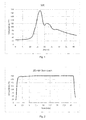
- Temperature curve of the temperature of the substrate during the NIR cure is illustrated in figure 1 .
- the curve illustrates that the maximum substrate temperature is only for a few seconds.
- temperature curves for the box-oven and IR techniques are illustrated in figures 2 and 3 .
- the curves illustrates that the maximum substrate temperature is for several seconds, close to a minure for IR cure and several minutes for box-oven cure.
- the electrically conductive composition on at least part of a substrate is exposed to a near infrared light for 30 seconds, preferably for 20 seconds and more preferably 10 seconds.
- NIR light used in the process according to present invention has a wavelength between 350 - 2250 nm, with peak wavelength around 750 nm.
- the intensity of the NIR light depends on the lamp used. Different suppliers might supply lamps with different intensity. Particularly preferred lamp to be used in the present invention is Adphos U-emitter.
- Example of commercially available NIR light suitable for use in the present invention is Adphos U emitter NB 18-250 from Adphos Innovative Technologies GmbH.
- the process according to the present invention may further comprise a drying step carried out before exposing said electrically conductive composition on the substrate to a near infrared light. Drying can be done with any conventional methods.
- An electrically conductive composition suitable for use in the process according to the present invention is in a form of a paste or an ink.
- the suitable electrically conductive composition may comprise a resin, electrically conductive particles, a solvent and additional additives.
- a typical electrically conductive ink (ECI) composition suitable for use in the process according to the present invention to form an electrical conductor comprises a resin from 0.5 to 15% by weight of the total weight of the composition, preferably from 1.0 to 10%; electrically conductive particles from 15 to 75% by weight of the total weight of the composition, preferably from 45 to 65%; and one or more organic solvent from 15 to 70% by weight of the total weight of the composition, preferably from 25 to 40%.
- Suitable electrically conductive ink (ECI) composition may further comprise additives from 0 to 5% by weight of the total weight of the composition, preferably from 0.1 to 3%.
- a typical electrically conductive paste (ECP) composition suitable for use in the process according to the present invention to form an electrical conductor comprises a resin from 0 to 15% by weight of the total weight of the composition, preferably from 0.1 to 15%, more preferably from 1 to 12%; electrically conductive particles from 45 to 97% by weight of the total weight of the composition, preferably from 60 to 95%.
- Suitable electrically conductive paste (ECP) composition may further comprise one or more organic solvent from 0 to 20% by weight of the total weight of the composition, preferably from 0.1 to 5%; and additives from 0 to 5% by weight of the total weight of the composition, preferably from 0.1 to 3%.
- a typical electrically conductive composition suitable for use in the process according to the present invention may comprise a resin.
- a typical electrically conductive ink (ECI) composition suitable for use in the process according to the present invention comprises a resin.
- Electrically conductive paste (ECP) may comprise a resin, but as an optional ingredient.
- Suitable resin for use in the present invention can be a thermoset or a thermoplastic resin.
- thermoplastic resins for use in the present invention can be selected from the group consisting of thermoplastic polyurethanes, polyesters, polyacrylates, polysiloxanes, halogenated vinyl or vinylidene polymers, polyamide copolymers, phenoxy resins, polyethers, polyketones, polyvinyl butyral, polyvinyl pyrrolidone, polyacrylates, polyimides, polyols, cellulose and mixtures thereof.
- thermoset resins for use in the present invention can be selected from the group consisting of epoxide, silicones, acrylates, BMI, benzoxazines, cyanate esters, olefins, phenolic resins, oxetanes, vinyl ethers and mixtures thereof.
- An electrically conductive composition suitable for use in the process according to the present invention may comprise a solvent.
- a typical electrically conductive ink (ECI) composition suitable for use in the process according to the present invention comprises a solvent.
- Electrically conductive paste (ECP) may comprise a solvent, but as an optional ingredient.
- Suitable solvent for use in the present invention can be selected from the group consisting of alcohols, ketones, esters, glycol esters, glycol ethers, ethers, acetates, carbonates and mixtures thereof.
- a solvent is selected from the group consisting of dipropylene glycol, ethylene glycol, diethylene glycol, triethylene glycol, hexylene glycol, 1-methoxy-2-propanol, diacetone alcohol, 2-ethyl-1,3-hexanediol, tridecanol, 1,2-octanediol, butyldiglycol, alpha-terpineol or beta-terpineol, 2-(2-butoxyethoxy)ethyl acetate, 2,2,4-trimetyl-1,3-pentanediol diisobutyrate, 1,2-propylene carbonate, carbitol acetate, butyl carbitol acetate, butyl carbitol, a
- a typical electrically conductive ink (ECI) or paste (ECP) composition suitable for use in the process according to the present invention comprises electronically conductive material.
- Suitable electronically conductive material for use in the present invention can be selected from the group consisting of silver, nickel, carbon, carbon black, graphite, graphene, copper, indium, indium alloys, gold, platinum, aluminum, iron, zinc, cobalt, lead, tin alloys, silver coated fillers such as silver coated copper, silver coated graphite, silver coated polymers and mixtures thereof.
- a typical electrically conductive ink (ECI) or paste (ECP) composition suitable for use in the process according to the present invention may further comprise a curing agent.
- a curing agent is present in the composition.
- Suitable curing agents for use in the present invention are any type of curing agents to initiate the reaction when heated, regardless of the possible cure mechanism.
- suitable curing agents for use in the present invention are any type of amide or amine - including epoxy-amine adducts, imidazoles, piperazines, piperidines, pyrazoles, purines, triazoles; dicarboxylic acids; anhydrides; mercaptanes; thiols; polysulfides; a lewis acid or salt, typically SbF 6 or PF 6 based iodonium or sulfonium salts, which create a super acid upon initiation/activation to trigger cure are used; peroxides; azo compounds, which dissociate upon heating and mixtures thereof.
- Typical electrically conductive ink (ECI) or paste (ECP) composition suitable for use in the process according to the present invention may further comprise one or more additive.
- Suitable additive for use in the present invention can be selected from the group consisting of rheological additives, wetting agents, dispersing agents, defoamers, adhesion promotors, anti-corrosion agents, inhibitors, stabilizers, fluxing agents, surfactants and mixtures thereof.
- an electrically conductive ink composition suitable for use in the process according to the present invention comprises,
- an electrically conductive ink composition suitable for use in the process according to the present invention comprises,
- an electrically conductive paste composition suitable for use in the process according to the present invention comprises,
- an electrically conductive paste composition suitable for use in the process according to the present invention comprises,
- the present invention relates to an electrical device, which comprises an electrical conductor formed by the process according to the present invention.
- the electrical device can be high speed printed electronic device.
- the electrical device can be any device comprising a printed circuit. More specifically, the electrical device can be a solar cell or solar module, which comprises an electrical conductor formed by the process according to the present invention.
- Figure 4 illustrates a comparison of resistance values of cured inks and pastes obtained with different curing techniques.
- Compositions were applied on the surface of the substrate (ITO coated silicon wafer) by screen printing. Applied compositions were exposed to NIR for 5-10 seconds and the compositions were dried or cured. In addition, additional samples of the same compositions were cured with conventional box-oven cure (20 minutes) and with IR cure (10 seconds). As the figure illustrates, the electrical properties are better with the compositions cured with NIR. At the same time, sintering of the compositions was observed when exposed to conventional box-oven cure for 20 minutes. Whereas, sintering was done within 10 seconds, with NIR cure. These results illustrate that process according to the present invention using NIR cure provides a very fast cure method, while ensuring optimal electrical properties.
- ECI is example 4 and ECP 1 and ECP 2 are variations of example 5.
- Figures 5 and 6 illustrate a comparison of resistance values of cured inks and pastes obtained with box-oven (20 minutes) and IR cure (10 seconds).
- Compositions were applied on the surface of the substrate (ITO coated silicon wafer) by screen printing and cured. Three different screen openings with different width were used i.e. 60 ⁇ m, 65 ⁇ m and 75 ⁇ m wide.
- the line resistance was calculated by dividing the resistance of the track (measured with 4-point probes) by the length of the track. The test results show that all line widths printed, the material cured with box-oven cure provides a much lower resistance than when the material is cured with IR at a much shorter time. This applies for both pastes and inks.
- Figures 1, 2 and 3 illustrates temperature profile of the substrate during box-oven, IR and NIR cure.
- NIR cure exposures the substrate for a higher temperature only for a short period of time (few seconds)
- box-oven and IR cure methods both exposure the substrate for higher temperature for longer period of time (from few minutes to several minutes), which may be detrimental for the delicate substrate.
- Temperature profiles were measured by fixating a thermocouple to the substrate (in this case an ITO coated silicon wafer) with heat resistant tape and run the curing profile.
- the thermocouple was connected with a PC and via PicoLog software the temperature profile was recorded.
- Heat sensitive substrates as active solar cells and plastics for example can withstand high temperatures for a short period of time. Therefore, process according to the present invention enables the use of very high conductive materials on these substrates without damaging the substrates.
- the cure step of the process according to the present invention can also be used as a post-processing step.
- the results exemplify that the additional NIR cure provides better conductivity of the material, and therefore, a better performance.
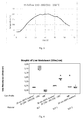
- Solar cells were printed on day one and cured by using conventional box-oven cure technique. Composition of example 4 was used herein. The efficiency of the cells were measured over time. A slow drop in performance is visual (see Figure 7 , every symbol represents a different cell). After 67 days (two samples) and after 82 days (one sample) some of the cells (noted by the symbols with a star in the graph) were post-cured with NIR for 3.6 seconds. Subsequently, the cell efficiency was measured again, and found higher than initial cell efficiency. Figure 7 illustrates these results.
- the test equipment used was a solar cell I-V tester from Industrial Vision Technology (S) Pte Ltd (Singapore) with a class AAA, constant lighting solar simulator.
Landscapes
- Chemical & Material Sciences (AREA)
- Life Sciences & Earth Sciences (AREA)
- Engineering & Computer Science (AREA)
- Materials Engineering (AREA)
- Wood Science & Technology (AREA)
- Organic Chemistry (AREA)
- Chemical Kinetics & Catalysis (AREA)
- General Chemical & Material Sciences (AREA)
- Inorganic Chemistry (AREA)
- Physics & Mathematics (AREA)
- Dispersion Chemistry (AREA)
- Spectroscopy & Molecular Physics (AREA)
- Inks, Pencil-Leads, Or Crayons (AREA)
- Conductive Materials (AREA)
- Sustainable Development (AREA)
- Sustainable Energy (AREA)
- Manufacturing Of Printed Wiring (AREA)
- Photovoltaic Devices (AREA)
Abstract
Description
- The present invention relates a process of forming electrical conductor on a substrate comprising the steps of a) providing a substrate; b) providing an electrically conductive composition; c) applying said electrically conductive composition to at least one part of said substrate; and d) exposing said electrically conductive composition on the substrate to a near infrared (NIR) light to form an electrically conductive pathway. NIR light cure provides improved electrical properties of the cured composition without damaging heat sensitive substrates in a very short time.
- Electrical conductors are formed on the substrate by printing or otherwise applying a conductive composition on to a surface of a substrate and curing the applied composition. Printed conductive inks and pastes, which are deposited on the delicate surfaces, are often difficult to cure and/or sinter because of their relative high curing temperatures. These high curing temperatures are not often compatible with delicate substrates used.
- One currently used curing technique in the printing process of the printed electronics is cure or drying in a box-oven process. Box-oven curing/drying technique is time consuming technique. Full cure/dryness may take up to one hour with box-oven technique.
- An alternative for the box-oven cure technique, is IR drying/curing, which is used more and more. IR cure is effective and a relative fast curing technique. IR drying/curing technique can be used in-line in a roll-to-roll manufacturing process, and is already much faster regarding drying/curing time. However, this technique increases the temperature of the substrates very intensely, which can be detrimental to the delicate substrates.
- Another currently used curing technique is a photonic flash, which is a fast curing technique. However, it is not possible to use this technique alone for high solvent based systems. For the flash cure technique, the solvents need to be evaporated. This solvent removal can be done by conventional box-oven drying or IR drying, which is as mentioned above, time consuming and/or may be detrimental to the delicate substrate.
- Therefore, there is still a need for a curing/drying technique to provide fast drying/cure without damaging the delicate substrate in the process.
-
-
Figure 1 illustrates a temperature profile on substrate with NIR cure. -
Figure 2 illustrates a temperature profile with box-oven cure. -
Figure 3 illustrates a temperature profile with IR reflow cure. -
Figure 4 illustrates a comparison of resistance values of ink and pastes obtained with different curing techniques. -
Figure 5 illustrates comparison between IR cure and box-oven cure for an electrically conductive ink. -
Figure 6 illustrates comparison between IR cure and box-oven cure for an electrically conductive paste. -
Figure 7 illustrates an effect of post-cure with NIR on solar cell efficiency. - The present invention relates to a process of forming an electrical conductor on a substrate comprising the steps of a) providing a substrate; b) providing an electrically conductive composition; c) applying said electrically conductive composition to at least one part of said substrate; and d) exposing said electrically conductive composition on the substrate to a near infrared light to form an electrical conductor.
- The present invention also relates to an electrical device comprising an electrical conductor formed by process according to the present invention. The electrical device can be a solar cell or solar module.
- In the following passages the present invention is described in more detail. Each aspect so described may be combined with any other aspect or aspects unless clearly indicated to the contrary. In particular, any feature indicated as being preferred or advantageous may be combined with any other feature or features indicated as being preferred or advantageous. In the context of the present invention, the terms used are to be construed in accordance with the following definitions, unless a context dictates otherwise.
- As used herein, the singular forms "a", "an" and "the" include both singular and plural referents unless the context clearly dictates otherwise.
- The terms "comprising", "comprises" and "comprised of" as used herein are synonymous with "including", "includes" or "containing", "contains", and are inclusive or open-ended and do not exclude additional, non-recited members, elements or method steps.
- The recitation of numerical end points includes all numbers and fractions subsumed within the respective ranges, as well as the recited end points.
- All percentages, parts, proportions and then like mentioned herein are based on weight unless otherwise indicated.
- When an amount, a concentration or other values or parameters is/are expressed in form of a range, a preferable range, or a preferable upper limit value and a preferable lower limit value, it should be understood as that any ranges obtained by combining any upper limit or preferable value with any lower limit or preferable value are specifically disclosed, without considering whether the obtained ranges are clearly mentioned in the context.
- All references cited in the present specification are hereby incorporated by reference in their entirety.
- Unless otherwise defined, all terms used in disclosing the invention, including technical and scientific terms, have the meaning as commonly understood by one of the ordinary skill in the art to which this invention belongs to. By means of further guidance, term definitions are included to better appreciate the teaching of the present invention.
- In accordance with the present invention, there is provided a process of forming electrical conductor on a substrate wherein an electrically conductive composition is exposed to a near infrared light to form an electrical conductor.
- Surprisingly the Applicant has discovered that the NIR cure technique does not only provide remarkably faster cure but also improves electrical properties of the cured composition.
- The present invention relates to a process of forming an electrical conductor on a substrate comprising the steps of: a) providing a substrate; b) providing an electrically conductive composition; c) applying said electrically conductive composition to at least one part of said substrate; and d) exposing said electrically conductive composition on the substrate to a near infrared light to form an electrical conductor.
- A process according to the present invention is directed to form an electrical conductor on a surface of wide variety of substrates, especially heat sensitive substrates. Material forming an electrical conductor have typically high drying/curing temperature, and therefore, substrates are exposed to the elevated temperatures for a long period of time during curing/drying step. This may be detrimental to heat sensitive substrates.
- Suitable substrates for use in the process according to the present invention are selected from the group consisting of plastics; polyethylene terephthalate; polyethylene; polyimide; polyvinylchloride; polystyrene; polyurethane; polycarbonate; textile; paper; cardboard; printed circuit boards (PCB) such as FR4 (formed from epoxy resin, woven glass fabric reinforcement and brominated flame retardant), FR5, HDI and any other type of epoxy or phenolic glass filler reinforced laminates; silicon wafers; transparent conductive oxide coated substrates and mixtures thereof.
- The process according to the present invention involves applying the electrically conductive composition to at least one part of the substrate.
- The electrically conductive composition can be applied onto the surface of the substrate by any suitable method. Preferably, the electrically conductive composition is applied by the method selected from the group consisting of screen printing, flexo gravure printing, roto gravure printing, off-set printing, roto-screen printing, gravure printing, inkjet printing, stencil printing, jet-dispensing, auger-valve dispensing, time-pressure dispensing, slot-die coating, laser induced forward transfer, pin-transfer, roll coating, comma coating, more preferably method is selected from the group consisting of flexo printing, roto screen printing, screen printing, stencil printing and gravure printing.
- The composition is applied on to at least one part of the substrate. The composition may cover whole surface of the substrate, or only a part of it. The composition may cover one specific area of the surface of the substrate, or it may cover symmetrical or asymmetrical patterns. Example of symmetrical patterns are finger and bus bar elements on the surface of the solar cells. Also any type of printed RFID antenna can benefit from the process according to the present invention.
- The process according to the present invention includes exposing the electrically conductive composition on the substrate to a near infrared light to cure the electrically conductive composition in order to form an electrical conductor. It has been discovered that the NIR cure does not only provide remarkably faster cure, but also improves electrical properties of the cured composition.
- The full cure can be reached in a very short time by using a NIR light source. The temperature of the substrate raises for the maximum temperature only for a short period of time, and therefore, the NIR cure technique is not detrimental to the delicate surfaces. Temperature curve of the temperature of the substrate during the NIR cure is illustrated in
figure 1 . The curve illustrates that the maximum substrate temperature is only for a few seconds. As a comparison, temperature curves for the box-oven and IR techniques are illustrated infigures 2 and3 . The curves illustrates that the maximum substrate temperature is for several seconds, close to a minure for IR cure and several minutes for box-oven cure. - In the process according to the present invention, the electrically conductive composition on at least part of a substrate is exposed to a near infrared light for 30 seconds, preferably for 20 seconds and more preferably 10 seconds.
- NIR light used in the process according to present invention has a wavelength between 350 - 2250 nm, with peak wavelength around 750 nm.
- The intensity of the NIR light depends on the lamp used. Different suppliers might supply lamps with different intensity. Particularly preferred lamp to be used in the present invention is Adphos U-emitter. Example of commercially available NIR light suitable for use in the present invention is Adphos U emitter NB 18-250 from Adphos Innovative Technologies GmbH.
- The process according to the present invention may further comprise a drying step carried out before exposing said electrically conductive composition on the substrate to a near infrared light. Drying can be done with any conventional methods.
- An electrically conductive composition suitable for use in the process according to the present invention is in a form of a paste or an ink. The suitable electrically conductive composition may comprise a resin, electrically conductive particles, a solvent and additional additives.
- A typical electrically conductive ink (ECI) composition suitable for use in the process according to the present invention to form an electrical conductor comprises a resin from 0.5 to 15% by weight of the total weight of the composition, preferably from 1.0 to 10%; electrically conductive particles from 15 to 75% by weight of the total weight of the composition, preferably from 45 to 65%; and one or more organic solvent from 15 to 70% by weight of the total weight of the composition, preferably from 25 to 40%. Suitable electrically conductive ink (ECI) composition may further comprise additives from 0 to 5% by weight of the total weight of the composition, preferably from 0.1 to 3%.
- A typical electrically conductive paste (ECP) composition suitable for use in the process according to the present invention to form an electrical conductor comprises a resin from 0 to 15% by weight of the total weight of the composition, preferably from 0.1 to 15%, more preferably from 1 to 12%; electrically conductive particles from 45 to 97% by weight of the total weight of the composition, preferably from 60 to 95%. Suitable electrically conductive paste (ECP) composition may further comprise one or more organic solvent from 0 to 20% by weight of the total weight of the composition, preferably from 0.1 to 5%; and additives from 0 to 5% by weight of the total weight of the composition, preferably from 0.1 to 3%.
- A typical electrically conductive composition suitable for use in the process according to the present invention may comprise a resin. A typical electrically conductive ink (ECI) composition suitable for use in the process according to the present invention comprises a resin. Electrically conductive paste (ECP) may comprise a resin, but as an optional ingredient.
- Suitable resin for use in the present invention can be a thermoset or a thermoplastic resin.
- Suitable thermoplastic resins for use in the present invention can be selected from the group consisting of thermoplastic polyurethanes, polyesters, polyacrylates, polysiloxanes, halogenated vinyl or vinylidene polymers, polyamide copolymers, phenoxy resins, polyethers, polyketones, polyvinyl butyral, polyvinyl pyrrolidone, polyacrylates, polyimides, polyols, cellulose and mixtures thereof.
- Suitable thermoset resins for use in the present invention can be selected from the group consisting of epoxide, silicones, acrylates, BMI, benzoxazines, cyanate esters, olefins, phenolic resins, oxetanes, vinyl ethers and mixtures thereof.
- An electrically conductive composition suitable for use in the process according to the present invention may comprise a solvent. A typical electrically conductive ink (ECI) composition suitable for use in the process according to the present invention comprises a solvent. Electrically conductive paste (ECP) may comprise a solvent, but as an optional ingredient.
- Suitable solvent for use in the present invention can be selected from the group consisting of alcohols, ketones, esters, glycol esters, glycol ethers, ethers, acetates, carbonates and mixtures thereof. Preferably, a solvent is selected from the group consisting of dipropylene glycol, ethylene glycol, diethylene glycol, triethylene glycol, hexylene glycol, 1-methoxy-2-propanol, diacetone alcohol, 2-ethyl-1,3-hexanediol, tridecanol, 1,2-octanediol, butyldiglycol, alpha-terpineol or beta-terpineol, 2-(2-butoxyethoxy)ethyl acetate, 2,2,4-trimetyl-1,3-pentanediol diisobutyrate, 1,2-propylene carbonate, carbitol acetate, butyl carbitol acetate, butyl carbitol, ethyl carbitol acetate, 2-phenoxy ethanol, hexylene glycol, dibutylphthalate, dibasic ester (DBE), dibasic ester 9 (DBE-9), dibasic ester 7 (DBE-7) and mixtures thereof.
- A typical electrically conductive ink (ECI) or paste (ECP) composition suitable for use in the process according to the present invention comprises electronically conductive material. Suitable electronically conductive material for use in the present invention can be selected from the group consisting of silver, nickel, carbon, carbon black, graphite, graphene, copper, indium, indium alloys, gold, platinum, aluminum, iron, zinc, cobalt, lead, tin alloys, silver coated fillers such as silver coated copper, silver coated graphite, silver coated polymers and mixtures thereof.
- A typical electrically conductive ink (ECI) or paste (ECP) composition suitable for use in the process according to the present invention may further comprise a curing agent. Especially, when the selected resin is a thermoset, a curing agent is present in the composition.
- Suitable curing agents for use in the present invention are any type of curing agents to initiate the reaction when heated, regardless of the possible cure mechanism. Examples of suitable curing agents for use in the present invention are any type of amide or amine - including epoxy-amine adducts, imidazoles, piperazines, piperidines, pyrazoles, purines, triazoles; dicarboxylic acids; anhydrides; mercaptanes; thiols; polysulfides; a lewis acid or salt, typically SbF6 or PF6 based iodonium or sulfonium salts, which create a super acid upon initiation/activation to trigger cure are used; peroxides; azo compounds, which dissociate upon heating and mixtures thereof.
- Typical electrically conductive ink (ECI) or paste (ECP) composition suitable for use in the process according to the present invention may further comprise one or more additive. Suitable additive for use in the present invention can be selected from the group consisting of rheological additives, wetting agents, dispersing agents, defoamers, adhesion promotors, anti-corrosion agents, inhibitors, stabilizers, fluxing agents, surfactants and mixtures thereof.
- In one embodiment, an electrically conductive ink composition suitable for use in the process according to the present invention comprises,
- a) from 0.5 to 15 wt.-% of resin;
- b) from 15 wt.-% to 75 wt.-% of electrically conductive silver particles; and
- c) from 10 to 70 wt.-% of one or more organic solvents,
wherein all wt.% are based on the total weight of the composition. - In another embodiment an electrically conductive ink composition suitable for use in the process according to the present invention comprises,
- a) from 0.5 to 15 wt.-% of resin;
- b) from 15 wt.-% to 75 wt.-% of electrically conductive silver particles;
- c) from 15 to 70 wt.-% of one or more organic solvents; and
- d) from 0.01 to 3 wt.-% of one or more additives,
wherein all wt.% are based on the total weight of the composition. - In one embodiment an electrically conductive paste composition suitable for use in the process according to the present invention comprises,
- a) from 0 to 15 wt.-% of resin, preferably from 0.1 to 15wt.%; and
- b) from 45 wt.-% to 97 wt.-% of electrically conductive silver particles,
wherein all wt.% are based on the total weight of the composition. - In another embodiment an electrically conductive paste composition suitable for use in the process according to the present invention comprises,
- a) from 0 to 15 wt.-% of resin, preferably from 0.1 to 15wt.%;
- b) from 45 wt.-% to 97 wt.-% of electrically conductive silver particles;
- c) from 0.1 to 15 wt.-% of one or more organic solvents, and
- d) from 0.01 to 3 wt.-% of one or more additives,
- The present invention relates to an electrical device, which comprises an electrical conductor formed by the process according to the present invention. The electrical device can be high speed printed electronic device. The electrical device can be any device comprising a printed circuit. More specifically, the electrical device can be a solar cell or solar module, which comprises an electrical conductor formed by the process according to the present invention.
- The examples described hereunder exemplify the properties of the compositions according to the embodiments of the present invention. Unless otherwise indicated, all parts and percentages in following examples, as well as throughout the description, are parts by weight or percentages by weight respectively.
- The following examples are included for purposes of illustration so that the disclosure may be more readily understood and are in no way to be intended to limit the scope of the disclosure unless otherwise specifically indicated.
-
Raw material Example 1 - ECI Phenoxy resin (PKHH) 10.184 Phenolic resin in solvent (PF 9132 KP) 0.359 Carbitol Acetate 28.138 Ag flake (GA238-11) 61.319 -
Raw material Example 2 - ECP Ag flake (FA-S-6) 88.10 Propylene carbonate 11.450 Luperox 100.440 Luperox 10 From Sigma Aldrich. -
Raw material Example 3 - ECI Disperbyk 110 0.550 DBE-9 21.150 Saran F-310 6.900 Ag flake (AA 3462) 54.520 Butyl glycol acetate 16.990 Estane 5715 0.890 -
Raw material Example 4 - ECI Resin 1.34 Carbitol acetate 3.28 Silver 94.69 Crayvallac Super 0.69 -
Raw material Example 5 - ECP Phenoxy resin 1.58 Carbitol acetate 4.40 Epoxy resin 11.80 Curing agent 0.21 Propylene carbonate 0.21 Epoxy resin 22.70 Ag flake P 554-19 85.50 Ag flake SAB 520 4.50 -
Figure 4 illustrates a comparison of resistance values of cured inks and pastes obtained with different curing techniques. Compositions were applied on the surface of the substrate (ITO coated silicon wafer) by screen printing. Applied compositions were exposed to NIR for 5-10 seconds and the compositions were dried or cured. In addition, additional samples of the same compositions were cured with conventional box-oven cure (20 minutes) and with IR cure (10 seconds). As the figure illustrates, the electrical properties are better with the compositions cured with NIR. At the same time, sintering of the compositions was observed when exposed to conventional box-oven cure for 20 minutes. Whereas, sintering was done within 10 seconds, with NIR cure. These results illustrate that process according to the present invention using NIR cure provides a very fast cure method, while ensuring optimal electrical properties. ECI is example 4 andECP 1 andECP 2 are variations of example 5. -
Raw material Example 5a - ECP1 Example 5b- ECP2 Phenoxy resin 1.58 1.58 Carbitol acetate 4.40 4.87 Epoxy resin 11.80 1.80 Curing agent 0.21 0.21 Propylene carbonate 0.21 0.21 Epoxy resin 22.70 2.70 Ag flake P 554-19 85.50 94.89 Ag flake SAB 520 4.50 5.00 -
Figures 5 and 6 illustrate a comparison of resistance values of cured inks and pastes obtained with box-oven (20 minutes) and IR cure (10 seconds). Compositions were applied on the surface of the substrate (ITO coated silicon wafer) by screen printing and cured. Three different screen openings with different width were used i.e. 60 µm, 65 µm and 75 µm wide. Subsequently, the line resistance was calculated by dividing the resistance of the track (measured with 4-point probes) by the length of the track. The test results show that all line widths printed, the material cured with box-oven cure provides a much lower resistance than when the material is cured with IR at a much shorter time. This applies for both pastes and inks. -
Figures 1, 2 and3 illustrates temperature profile of the substrate during box-oven, IR and NIR cure. NIR cure exposures the substrate for a higher temperature only for a short period of time (few seconds), whereas both box-oven and IR cure methods both exposure the substrate for higher temperature for longer period of time (from few minutes to several minutes), which may be detrimental for the delicate substrate. - Temperature profiles were measured by fixating a thermocouple to the substrate (in this case an ITO coated silicon wafer) with heat resistant tape and run the curing profile. The thermocouple was connected with a PC and via PicoLog software the temperature profile was recorded.
- Heat sensitive substrates as active solar cells and plastics for example, can withstand high temperatures for a short period of time. Therefore, process according to the present invention enables the use of very high conductive materials on these substrates without damaging the substrates.
- The cure step of the process according to the present invention can also be used as a post-processing step. This means that curable materials, which have already been cured with different techniques can be provided an additional NIR cure. The results exemplify that the additional NIR cure provides better conductivity of the material, and therefore, a better performance.
- Solar cells were printed on day one and cured by using conventional box-oven cure technique. Composition of example 4 was used herein. The efficiency of the cells were measured over time. A slow drop in performance is visual (see
Figure 7 , every symbol represents a different cell). After 67 days (two samples) and after 82 days (one sample) some of the cells (noted by the symbols with a star in the graph) were post-cured with NIR for 3.6 seconds. Subsequently, the cell efficiency was measured again, and found higher than initial cell efficiency.Figure 7 illustrates these results. - Efficiency of the cells was measured with I-V testing. The test equipment used was a solar cell I-V tester from Industrial Vision Technology (S) Pte Ltd (Singapore) with a class AAA, constant lighting solar simulator.
Claims (10)
- A process of forming electrical conductor on a substrate comprising the steps of:a) providing a substrate;b) providing an electrically conductive composition;c) applying said electrically conductive composition to at least one part of said substrate; andd) exposing said electrically conductive composition on the substrate to a near infrared light to form an electrical conductor.
- A process according to claim 1, wherein said process further comprises a drying step carried out before exposing said electrically conductive composition on the substrate to a near infrared light.
- A process according to claim 1 or 2, wherein said electrically conductive composition on said substrate is exposed to a near infrared light for 30 seconds, preferably for 20 seconds and more preferably 10 seconds.
- A process according to any of claims 1 to 3, wherein said substrate is selected from the group consisting of plastics, polyethylene terephthalate, polyethylene, polyimide, polyvinylchloride, polystyrene, polyurethane, textile, paper, cardboard, printed circuit boards (PCB), silicon wafers, transparent conductive oxide coated substrates and mixtures thereof.
- A process according to any of claims 1 to 4, wherein said electrically conductive composition is applied on to the substrate by the method selected from the group consisting of screen printing, flexo gravure printing, roto gravure printing, off-set printing, roto-screen printing, gravure printing, inkjet printing, stencil printing, jet-dispensing, auger-valve dispensing, time-pressure dispensing, slot-die coating, laser induced forward transfer, pin-transfer, roll coating, comma coating, preferably method is selected from the group consisting of flexo printing, roto screen printing, screen printing, stencil printing and gravure printing.
- A process according to any of claims 1 to 5, wherein said electrically conductive composition is in a form of a paste or an ink.
- A process according to claim 6, wherein said electrically conductive composition is an ink and comprisesa) from 0.1 to 15 wt.-% of a resin;b) from 15 wt.-% to 75 wt.-% of electrically conductive particles; andc) from 10 to 70 wt.-% of one or more organic solvents,
wherein all wt.% are based on total weight of the composition. - A process according to claim 6, wherein said electrically conductive composition is a paste and comprisesa) from 0 to 15 wt.-% of a resin, preferably from 0.1 to 15 wt.-%; andb) from 45 wt.-% to 97 wt.-% of electrically conductive particles,c) from 0 to 15 wt% of one or more organic solvents,
wherein all wt.% are based on total weight of the composition. - An electrical device comprising electrical conductor formed by process according to any preceding claims 1 to 8.
- An electrical device according to claim 9, wherein said electrical device is a solar cell or solar module.
Priority Applications (7)
| Application Number | Priority Date | Filing Date | Title |
|---|---|---|---|
| EP16183752.1A EP3282453B1 (en) | 2016-08-11 | 2016-08-11 | Improved processing of polymer based inks and pastes |
| TW106124426A TWI877095B (en) | 2016-08-11 | 2017-07-20 | Improved processing of polymer based inks and pastes |
| JP2019507332A JP7523218B2 (en) | 2016-08-11 | 2017-07-26 | Improved Processing of Polymer-Based Inks and Pastes - Patent application |
| CN201780048661.3A CN109564792A (en) | 2016-08-11 | 2017-07-26 | The improvement of ink and paste based on polymer is processed |
| PCT/EP2017/068828 WO2018028984A1 (en) | 2016-08-11 | 2017-07-26 | Improved processing of polymer based inks and pastes |
| KR1020197006854A KR20190040235A (en) | 2016-08-11 | 2017-07-26 | Improved processing of polymer-based inks and pastes |
| US16/270,947 US10920098B2 (en) | 2016-08-11 | 2019-02-08 | Processing of polymer based inks and pastes |
Applications Claiming Priority (1)
| Application Number | Priority Date | Filing Date | Title |
|---|---|---|---|
| EP16183752.1A EP3282453B1 (en) | 2016-08-11 | 2016-08-11 | Improved processing of polymer based inks and pastes |
Publications (2)
| Publication Number | Publication Date |
|---|---|
| EP3282453A1 true EP3282453A1 (en) | 2018-02-14 |
| EP3282453B1 EP3282453B1 (en) | 2023-07-12 |
Family
ID=56958720
Family Applications (1)
| Application Number | Title | Priority Date | Filing Date |
|---|---|---|---|
| EP16183752.1A Active EP3282453B1 (en) | 2016-08-11 | 2016-08-11 | Improved processing of polymer based inks and pastes |
Country Status (7)
| Country | Link |
|---|---|
| US (1) | US10920098B2 (en) |
| EP (1) | EP3282453B1 (en) |
| JP (1) | JP7523218B2 (en) |
| KR (1) | KR20190040235A (en) |
| CN (1) | CN109564792A (en) |
| TW (1) | TWI877095B (en) |
| WO (1) | WO2018028984A1 (en) |
Families Citing this family (2)
| Publication number | Priority date | Publication date | Assignee | Title |
|---|---|---|---|---|
| KR102271417B1 (en) * | 2016-06-08 | 2021-07-02 | 아그파-게바에르트 엔.브이. | Set of inkjet inks for making conductive layers or patterns |
| US12046575B2 (en) | 2019-05-01 | 2024-07-23 | Io Tech Group Ltd. | Method to electrically connect chip with top connectors using 3D printing |
Citations (6)
| Publication number | Priority date | Publication date | Assignee | Title |
|---|---|---|---|---|
| US20030178221A1 (en) * | 2002-03-21 | 2003-09-25 | Chiu Cindy Chia-Wen | Anisotropically conductive film |
| EP1594351A2 (en) * | 2004-05-06 | 2005-11-09 | National Starch and Chemical Investment Holding Corporation | Compositions for use in electronics devices |
| EP1993144A1 (en) * | 2006-03-07 | 2008-11-19 | Murata Manufacturing Co. Ltd. | Conductive paste and solar cell |
| US20100294353A1 (en) * | 2009-05-21 | 2010-11-25 | E. I. Du Pont De Nemours And Company | Conductive paste for solar cell electrode |
| WO2016024793A2 (en) * | 2014-08-11 | 2016-02-18 | 주식회사 엔앤비 | Production method for transparent electrically-conductive film using multistage light irradiation |
| US20160155868A1 (en) * | 2013-07-25 | 2016-06-02 | Namics Corporation | Crystalline silicon solar cell and method for producing same |
Family Cites Families (11)
| Publication number | Priority date | Publication date | Assignee | Title |
|---|---|---|---|---|
| JP2000234075A (en) * | 1999-02-16 | 2000-08-29 | Toppan Forms Co Ltd | Fixing method of thermosetting conductive ink on paper substrate |
| JP2001308496A (en) * | 2000-04-19 | 2001-11-02 | Sony Corp | Method of forming electrodes on functional film |
| CN101395723A (en) * | 2006-03-07 | 2009-03-25 | 株式会社村田制作所 | Conductive paste and solar cell |
| JP5341500B2 (en) * | 2008-12-24 | 2013-11-13 | ナミックス株式会社 | Screen printing method and apparatus |
| JP5614101B2 (en) * | 2010-05-24 | 2014-10-29 | 大日本印刷株式会社 | Method for manufacturing conductive substrate |
| JP2013243279A (en) * | 2012-05-22 | 2013-12-05 | Namics Corp | Conductive paste for forming solar cell electrode |
| JP6311310B2 (en) * | 2012-10-04 | 2018-04-18 | 東レ株式会社 | Manufacturing method of conductive pattern |
| JP5610112B1 (en) * | 2013-01-30 | 2014-10-22 | Dic株式会社 | Conductive paste, conductive pattern forming method, and printed conductive pattern |
| JP5955791B2 (en) * | 2013-02-12 | 2016-07-20 | 株式会社ノリタケカンパニーリミテド | Paste composition and solar cell |
| US9190188B2 (en) | 2013-06-13 | 2015-11-17 | E I Du Pont De Nemours And Company | Photonic sintering of polymer thick film copper conductor compositions |
| KR101595895B1 (en) * | 2014-08-11 | 2016-02-19 | 주식회사 엔앤비 | Film for transparent electrode with welded silver nanowire by light sintering, Dispersion liquid for welding silver nanowire, and Welding method of silver nanowire by light sintering |
-
2016
- 2016-08-11 EP EP16183752.1A patent/EP3282453B1/en active Active
-
2017
- 2017-07-20 TW TW106124426A patent/TWI877095B/en active
- 2017-07-26 KR KR1020197006854A patent/KR20190040235A/en not_active Ceased
- 2017-07-26 CN CN201780048661.3A patent/CN109564792A/en active Pending
- 2017-07-26 WO PCT/EP2017/068828 patent/WO2018028984A1/en not_active Ceased
- 2017-07-26 JP JP2019507332A patent/JP7523218B2/en active Active
-
2019
- 2019-02-08 US US16/270,947 patent/US10920098B2/en active Active
Patent Citations (6)
| Publication number | Priority date | Publication date | Assignee | Title |
|---|---|---|---|---|
| US20030178221A1 (en) * | 2002-03-21 | 2003-09-25 | Chiu Cindy Chia-Wen | Anisotropically conductive film |
| EP1594351A2 (en) * | 2004-05-06 | 2005-11-09 | National Starch and Chemical Investment Holding Corporation | Compositions for use in electronics devices |
| EP1993144A1 (en) * | 2006-03-07 | 2008-11-19 | Murata Manufacturing Co. Ltd. | Conductive paste and solar cell |
| US20100294353A1 (en) * | 2009-05-21 | 2010-11-25 | E. I. Du Pont De Nemours And Company | Conductive paste for solar cell electrode |
| US20160155868A1 (en) * | 2013-07-25 | 2016-06-02 | Namics Corporation | Crystalline silicon solar cell and method for producing same |
| WO2016024793A2 (en) * | 2014-08-11 | 2016-02-18 | 주식회사 엔앤비 | Production method for transparent electrically-conductive film using multistage light irradiation |
Also Published As
| Publication number | Publication date |
|---|---|
| US10920098B2 (en) | 2021-02-16 |
| WO2018028984A1 (en) | 2018-02-15 |
| KR20190040235A (en) | 2019-04-17 |
| JP7523218B2 (en) | 2024-07-26 |
| JP2019532490A (en) | 2019-11-07 |
| TW201829659A (en) | 2018-08-16 |
| TWI877095B (en) | 2025-03-21 |
| CN109564792A (en) | 2019-04-02 |
| US20190169457A1 (en) | 2019-06-06 |
| EP3282453B1 (en) | 2023-07-12 |
Similar Documents
| Publication | Publication Date | Title |
|---|---|---|
| KR102260343B1 (en) | Emi shielding composition and process for applying it | |
| JP5775494B2 (en) | Silver ion diffusion suppression layer forming composition, silver ion diffusion suppression layer film, wiring board, electronic device, conductive film laminate, and touch panel | |
| TWI420239B (en) | Improved hot melt compositions | |
| JP6426737B2 (en) | Bonding of electronic components and patterned nanowire transparent conductors | |
| WO2008051719A1 (en) | Conductive ink formulations | |
| US10920098B2 (en) | Processing of polymer based inks and pastes | |
| US20120309866A1 (en) | Solder ink and electronic device package using same | |
| KR20150000823A (en) | Method of improving sheet resistivity of printed conductive inks | |
| US20050247916A1 (en) | Compositions for use in electronics devices | |
| JP6849221B2 (en) | Metal thin film manufacturing method and conductive structure | |
| DE102016225051A1 (en) | INTERMEDIATE COMPOSITION FOR ELECTRONIC PRINTING | |
| JP2016216725A (en) | Curable composition for inkjet and method of manufacturing electronic component | |
| WO2017003820A1 (en) | Patterned overcoat layer | |
| US20180139855A1 (en) | Electronic devices comprising a via and methods of forming such electronic devices | |
| KR102117250B1 (en) | Composition for preparing transparent conductive layer and manufacturing method of transparent conductive structure using the same | |
| US20240357742A1 (en) | Printed product, preparation method therefor, and use thereof | |
| JP2012167268A (en) | Curable composition for inkjet and method for producing electronic component | |
| JP2009252494A (en) | Manufacturing method of base material with conductive film and base material with conductive film | |
| EP3296364B1 (en) | Uv curable interlayer composition for printed electronics application | |
| JP6039023B2 (en) | Curable composition for inkjet and method for producing printed wiring board | |
| Sutter | Inkjet fabrication of printed circuit boards | |
| Zainal et al. | Using Halogen Lamp and Oven | |
| KR20260062101A (en) | Photodegradation based non-conductive adhesive for micro-led display and method of manufacturing same | |
| JPH03137175A (en) | Electron radiation curing type electrically conductive paste | |
| JPH03137173A (en) | Electron radiation curing type electrically conductive paste |
Legal Events
| Date | Code | Title | Description |
|---|---|---|---|
| PUAI | Public reference made under article 153(3) epc to a published international application that has entered the european phase |
Free format text: ORIGINAL CODE: 0009012 |
|
| STAA | Information on the status of an ep patent application or granted ep patent |
Free format text: STATUS: THE APPLICATION HAS BEEN PUBLISHED |
|
| AK | Designated contracting states |
Kind code of ref document: A1 Designated state(s): AL AT BE BG CH CY CZ DE DK EE ES FI FR GB GR HR HU IE IS IT LI LT LU LV MC MK MT NL NO PL PT RO RS SE SI SK SM TR |
|
| AX | Request for extension of the european patent |
Extension state: BA ME |
|
| STAA | Information on the status of an ep patent application or granted ep patent |
Free format text: STATUS: REQUEST FOR EXAMINATION WAS MADE |
|
| 17P | Request for examination filed |
Effective date: 20180814 |
|
| STAA | Information on the status of an ep patent application or granted ep patent |
Free format text: STATUS: EXAMINATION IS IN PROGRESS |
|
| 17Q | First examination report despatched |
Effective date: 20200911 |
|
| GRAP | Despatch of communication of intention to grant a patent |
Free format text: ORIGINAL CODE: EPIDOSNIGR1 |
|
| STAA | Information on the status of an ep patent application or granted ep patent |
Free format text: STATUS: GRANT OF PATENT IS INTENDED |
|
| INTG | Intention to grant announced |
Effective date: 20230315 |
|
| GRAS | Grant fee paid |
Free format text: ORIGINAL CODE: EPIDOSNIGR3 |
|
| GRAA | (expected) grant |
Free format text: ORIGINAL CODE: 0009210 |
|
| STAA | Information on the status of an ep patent application or granted ep patent |
Free format text: STATUS: THE PATENT HAS BEEN GRANTED |
|
| AK | Designated contracting states |
Kind code of ref document: B1 Designated state(s): AL AT BE BG CH CY CZ DE DK EE ES FI FR GB GR HR HU IE IS IT LI LT LU LV MC MK MT NL NO PL PT RO RS SE SI SK SM TR |
|
| P01 | Opt-out of the competence of the unified patent court (upc) registered |
Effective date: 20230531 |
|
| REG | Reference to a national code |
Ref country code: CH Ref legal event code: EP |
|
| REG | Reference to a national code |
Ref country code: IE Ref legal event code: FG4D |
|
| REG | Reference to a national code |
Ref country code: DE Ref legal event code: R096 Ref document number: 602016080939 Country of ref document: DE |
|
| REG | Reference to a national code |
Ref country code: LT Ref legal event code: MG9D |
|
| REG | Reference to a national code |
Ref country code: NL Ref legal event code: MP Effective date: 20230712 |
|
| REG | Reference to a national code |
Ref country code: AT Ref legal event code: MK05 Ref document number: 1588019 Country of ref document: AT Kind code of ref document: T Effective date: 20230712 |
|
| PG25 | Lapsed in a contracting state [announced via postgrant information from national office to epo] |
Ref country code: NL Free format text: LAPSE BECAUSE OF FAILURE TO SUBMIT A TRANSLATION OF THE DESCRIPTION OR TO PAY THE FEE WITHIN THE PRESCRIBED TIME-LIMIT Effective date: 20230712 |
|
| PG25 | Lapsed in a contracting state [announced via postgrant information from national office to epo] |
Ref country code: GR Free format text: LAPSE BECAUSE OF FAILURE TO SUBMIT A TRANSLATION OF THE DESCRIPTION OR TO PAY THE FEE WITHIN THE PRESCRIBED TIME-LIMIT Effective date: 20231013 |
|
| PG25 | Lapsed in a contracting state [announced via postgrant information from national office to epo] |
Ref country code: ES Free format text: LAPSE BECAUSE OF FAILURE TO SUBMIT A TRANSLATION OF THE DESCRIPTION OR TO PAY THE FEE WITHIN THE PRESCRIBED TIME-LIMIT Effective date: 20230712 |
|
| PG25 | Lapsed in a contracting state [announced via postgrant information from national office to epo] |
Ref country code: IS Free format text: LAPSE BECAUSE OF FAILURE TO SUBMIT A TRANSLATION OF THE DESCRIPTION OR TO PAY THE FEE WITHIN THE PRESCRIBED TIME-LIMIT Effective date: 20231112 |
|
| PG25 | Lapsed in a contracting state [announced via postgrant information from national office to epo] |
Ref country code: SE Free format text: LAPSE BECAUSE OF FAILURE TO SUBMIT A TRANSLATION OF THE DESCRIPTION OR TO PAY THE FEE WITHIN THE PRESCRIBED TIME-LIMIT Effective date: 20230712 Ref country code: RS Free format text: LAPSE BECAUSE OF FAILURE TO SUBMIT A TRANSLATION OF THE DESCRIPTION OR TO PAY THE FEE WITHIN THE PRESCRIBED TIME-LIMIT Effective date: 20230712 Ref country code: PT Free format text: LAPSE BECAUSE OF FAILURE TO SUBMIT A TRANSLATION OF THE DESCRIPTION OR TO PAY THE FEE WITHIN THE PRESCRIBED TIME-LIMIT Effective date: 20231113 Ref country code: NO Free format text: LAPSE BECAUSE OF FAILURE TO SUBMIT A TRANSLATION OF THE DESCRIPTION OR TO PAY THE FEE WITHIN THE PRESCRIBED TIME-LIMIT Effective date: 20231012 Ref country code: LV Free format text: LAPSE BECAUSE OF FAILURE TO SUBMIT A TRANSLATION OF THE DESCRIPTION OR TO PAY THE FEE WITHIN THE PRESCRIBED TIME-LIMIT Effective date: 20230712 Ref country code: LT Free format text: LAPSE BECAUSE OF FAILURE TO SUBMIT A TRANSLATION OF THE DESCRIPTION OR TO PAY THE FEE WITHIN THE PRESCRIBED TIME-LIMIT Effective date: 20230712 Ref country code: IS Free format text: LAPSE BECAUSE OF FAILURE TO SUBMIT A TRANSLATION OF THE DESCRIPTION OR TO PAY THE FEE WITHIN THE PRESCRIBED TIME-LIMIT Effective date: 20231112 Ref country code: HR Free format text: LAPSE BECAUSE OF FAILURE TO SUBMIT A TRANSLATION OF THE DESCRIPTION OR TO PAY THE FEE WITHIN THE PRESCRIBED TIME-LIMIT Effective date: 20230712 Ref country code: GR Free format text: LAPSE BECAUSE OF FAILURE TO SUBMIT A TRANSLATION OF THE DESCRIPTION OR TO PAY THE FEE WITHIN THE PRESCRIBED TIME-LIMIT Effective date: 20231013 Ref country code: FI Free format text: LAPSE BECAUSE OF FAILURE TO SUBMIT A TRANSLATION OF THE DESCRIPTION OR TO PAY THE FEE WITHIN THE PRESCRIBED TIME-LIMIT Effective date: 20230712 Ref country code: ES Free format text: LAPSE BECAUSE OF FAILURE TO SUBMIT A TRANSLATION OF THE DESCRIPTION OR TO PAY THE FEE WITHIN THE PRESCRIBED TIME-LIMIT Effective date: 20230712 Ref country code: AT Free format text: LAPSE BECAUSE OF FAILURE TO SUBMIT A TRANSLATION OF THE DESCRIPTION OR TO PAY THE FEE WITHIN THE PRESCRIBED TIME-LIMIT Effective date: 20230712 |
|
| PG25 | Lapsed in a contracting state [announced via postgrant information from national office to epo] |
Ref country code: PL Free format text: LAPSE BECAUSE OF FAILURE TO SUBMIT A TRANSLATION OF THE DESCRIPTION OR TO PAY THE FEE WITHIN THE PRESCRIBED TIME-LIMIT Effective date: 20230712 |
|
| REG | Reference to a national code |
Ref country code: CH Ref legal event code: PL |
|
| REG | Reference to a national code |
Ref country code: DE Ref legal event code: R097 Ref document number: 602016080939 Country of ref document: DE |
|
| PG25 | Lapsed in a contracting state [announced via postgrant information from national office to epo] |
Ref country code: LU Free format text: LAPSE BECAUSE OF NON-PAYMENT OF DUE FEES Effective date: 20230811 |
|
| PG25 | Lapsed in a contracting state [announced via postgrant information from national office to epo] |
Ref country code: SM Free format text: LAPSE BECAUSE OF FAILURE TO SUBMIT A TRANSLATION OF THE DESCRIPTION OR TO PAY THE FEE WITHIN THE PRESCRIBED TIME-LIMIT Effective date: 20230712 Ref country code: RO Free format text: LAPSE BECAUSE OF FAILURE TO SUBMIT A TRANSLATION OF THE DESCRIPTION OR TO PAY THE FEE WITHIN THE PRESCRIBED TIME-LIMIT Effective date: 20230712 Ref country code: LU Free format text: LAPSE BECAUSE OF NON-PAYMENT OF DUE FEES Effective date: 20230811 Ref country code: EE Free format text: LAPSE BECAUSE OF FAILURE TO SUBMIT A TRANSLATION OF THE DESCRIPTION OR TO PAY THE FEE WITHIN THE PRESCRIBED TIME-LIMIT Effective date: 20230712 Ref country code: DK Free format text: LAPSE BECAUSE OF FAILURE TO SUBMIT A TRANSLATION OF THE DESCRIPTION OR TO PAY THE FEE WITHIN THE PRESCRIBED TIME-LIMIT Effective date: 20230712 Ref country code: CZ Free format text: LAPSE BECAUSE OF FAILURE TO SUBMIT A TRANSLATION OF THE DESCRIPTION OR TO PAY THE FEE WITHIN THE PRESCRIBED TIME-LIMIT Effective date: 20230712 Ref country code: CH Free format text: LAPSE BECAUSE OF NON-PAYMENT OF DUE FEES Effective date: 20230831 Ref country code: SK Free format text: LAPSE BECAUSE OF FAILURE TO SUBMIT A TRANSLATION OF THE DESCRIPTION OR TO PAY THE FEE WITHIN THE PRESCRIBED TIME-LIMIT Effective date: 20230712 Ref country code: MC Free format text: LAPSE BECAUSE OF FAILURE TO SUBMIT A TRANSLATION OF THE DESCRIPTION OR TO PAY THE FEE WITHIN THE PRESCRIBED TIME-LIMIT Effective date: 20230712 |
|
| REG | Reference to a national code |
Ref country code: BE Ref legal event code: MM Effective date: 20230831 |
|
| PLBE | No opposition filed within time limit |
Free format text: ORIGINAL CODE: 0009261 |
|
| STAA | Information on the status of an ep patent application or granted ep patent |
Free format text: STATUS: NO OPPOSITION FILED WITHIN TIME LIMIT |
|
| REG | Reference to a national code |
Ref country code: IE Ref legal event code: MM4A |
|
| PG25 | Lapsed in a contracting state [announced via postgrant information from national office to epo] |
Ref country code: IT Free format text: LAPSE BECAUSE OF FAILURE TO SUBMIT A TRANSLATION OF THE DESCRIPTION OR TO PAY THE FEE WITHIN THE PRESCRIBED TIME-LIMIT Effective date: 20230712 |
|
| 26N | No opposition filed |
Effective date: 20240415 |
|
| GBPC | Gb: european patent ceased through non-payment of renewal fee |
Effective date: 20231012 |
|
| PG25 | Lapsed in a contracting state [announced via postgrant information from national office to epo] |
Ref country code: IE Free format text: LAPSE BECAUSE OF NON-PAYMENT OF DUE FEES Effective date: 20230811 |
|
| PG25 | Lapsed in a contracting state [announced via postgrant information from national office to epo] |
Ref country code: GB Free format text: LAPSE BECAUSE OF NON-PAYMENT OF DUE FEES Effective date: 20231012 |
|
| PG25 | Lapsed in a contracting state [announced via postgrant information from national office to epo] |
Ref country code: IE Free format text: LAPSE BECAUSE OF NON-PAYMENT OF DUE FEES Effective date: 20230811 Ref country code: GB Free format text: LAPSE BECAUSE OF NON-PAYMENT OF DUE FEES Effective date: 20231012 Ref country code: SI Free format text: LAPSE BECAUSE OF FAILURE TO SUBMIT A TRANSLATION OF THE DESCRIPTION OR TO PAY THE FEE WITHIN THE PRESCRIBED TIME-LIMIT Effective date: 20230712 |
|
| PG25 | Lapsed in a contracting state [announced via postgrant information from national office to epo] |
Ref country code: BE Free format text: LAPSE BECAUSE OF NON-PAYMENT OF DUE FEES Effective date: 20230831 |
|
| PG25 | Lapsed in a contracting state [announced via postgrant information from national office to epo] |
Ref country code: BG Free format text: LAPSE BECAUSE OF FAILURE TO SUBMIT A TRANSLATION OF THE DESCRIPTION OR TO PAY THE FEE WITHIN THE PRESCRIBED TIME-LIMIT Effective date: 20230712 |
|
| PG25 | Lapsed in a contracting state [announced via postgrant information from national office to epo] |
Ref country code: BG Free format text: LAPSE BECAUSE OF FAILURE TO SUBMIT A TRANSLATION OF THE DESCRIPTION OR TO PAY THE FEE WITHIN THE PRESCRIBED TIME-LIMIT Effective date: 20230712 |
|
| PG25 | Lapsed in a contracting state [announced via postgrant information from national office to epo] |
Ref country code: CY Free format text: LAPSE BECAUSE OF FAILURE TO SUBMIT A TRANSLATION OF THE DESCRIPTION OR TO PAY THE FEE WITHIN THE PRESCRIBED TIME-LIMIT; INVALID AB INITIO Effective date: 20160811 |
|
| PG25 | Lapsed in a contracting state [announced via postgrant information from national office to epo] |
Ref country code: HU Free format text: LAPSE BECAUSE OF FAILURE TO SUBMIT A TRANSLATION OF THE DESCRIPTION OR TO PAY THE FEE WITHIN THE PRESCRIBED TIME-LIMIT; INVALID AB INITIO Effective date: 20160811 |
|
| PGFP | Annual fee paid to national office [announced via postgrant information from national office to epo] |
Ref country code: DE Payment date: 20250820 Year of fee payment: 10 |
|
| PGFP | Annual fee paid to national office [announced via postgrant information from national office to epo] |
Ref country code: FR Payment date: 20250829 Year of fee payment: 10 |
|
| PG25 | Lapsed in a contracting state [announced via postgrant information from national office to epo] |
Ref country code: TR Free format text: LAPSE BECAUSE OF FAILURE TO SUBMIT A TRANSLATION OF THE DESCRIPTION OR TO PAY THE FEE WITHIN THE PRESCRIBED TIME-LIMIT Effective date: 20230712 |