EP3279958A1 - Magnetoresistive effect element - Google Patents
Magnetoresistive effect element Download PDFInfo
- Publication number
- EP3279958A1 EP3279958A1 EP16772746.0A EP16772746A EP3279958A1 EP 3279958 A1 EP3279958 A1 EP 3279958A1 EP 16772746 A EP16772746 A EP 16772746A EP 3279958 A1 EP3279958 A1 EP 3279958A1
- Authority
- EP
- European Patent Office
- Prior art keywords
- tunnel barrier
- barrier layer
- ferromagnetic metal
- metal layer
- magnetoresistance effect
- Prior art date
- Legal status (The legal status is an assumption and is not a legal conclusion. Google has not performed a legal analysis and makes no representation as to the accuracy of the status listed.)
- Granted
Links
Images





Classifications
-
- H—ELECTRICITY
- H10—SEMICONDUCTOR DEVICES; ELECTRIC SOLID-STATE DEVICES NOT OTHERWISE PROVIDED FOR
- H10N—ELECTRIC SOLID-STATE DEVICES NOT OTHERWISE PROVIDED FOR
- H10N50/00—Galvanomagnetic devices
- H10N50/80—Constructional details
- H10N50/85—Materials of the active region
-
- G—PHYSICS
- G01—MEASURING; TESTING
- G01R—MEASURING ELECTRIC VARIABLES; MEASURING MAGNETIC VARIABLES
- G01R33/00—Arrangements or instruments for measuring magnetic variables
- G01R33/02—Measuring direction or magnitude of magnetic fields or magnetic flux
- G01R33/06—Measuring direction or magnitude of magnetic fields or magnetic flux using galvano-magnetic devices
- G01R33/09—Magnetoresistive devices
-
- G—PHYSICS
- G11—INFORMATION STORAGE
- G11B—INFORMATION STORAGE BASED ON RELATIVE MOVEMENT BETWEEN RECORD CARRIER AND TRANSDUCER
- G11B5/00—Recording by magnetisation or demagnetisation of a record carrier; Reproducing by magnetic means; Record carriers therefor
- G11B5/127—Structure or manufacture of heads, e.g. inductive
- G11B5/33—Structure or manufacture of flux-sensitive heads, i.e. for reproduction only; Combination of such heads with means for recording or erasing only
- G11B5/39—Structure or manufacture of flux-sensitive heads, i.e. for reproduction only; Combination of such heads with means for recording or erasing only using magneto-resistive devices or effects
-
- G—PHYSICS
- G11—INFORMATION STORAGE
- G11C—STATIC STORES
- G11C11/00—Digital stores characterised by the use of particular electric or magnetic storage elements; Storage elements therefor
- G11C11/02—Digital stores characterised by the use of particular electric or magnetic storage elements; Storage elements therefor using magnetic elements
- G11C11/16—Digital stores characterised by the use of particular electric or magnetic storage elements; Storage elements therefor using magnetic elements using elements in which the storage effect is based on magnetic spin effect
-
- H—ELECTRICITY
- H01—ELECTRIC ELEMENTS
- H01F—MAGNETS; INDUCTANCES; TRANSFORMERS; SELECTION OF MATERIALS FOR THEIR MAGNETIC PROPERTIES
- H01F10/00—Thin magnetic films, e.g. of one-domain structure
- H01F10/08—Thin magnetic films, e.g. of one-domain structure characterised by magnetic layers
- H01F10/10—Thin magnetic films, e.g. of one-domain structure characterised by magnetic layers characterised by the composition
- H01F10/12—Thin magnetic films, e.g. of one-domain structure characterised by magnetic layers characterised by the composition being metals or alloys
- H01F10/16—Thin magnetic films, e.g. of one-domain structure characterised by magnetic layers characterised by the composition being metals or alloys containing cobalt
-
- H—ELECTRICITY
- H01—ELECTRIC ELEMENTS
- H01F—MAGNETS; INDUCTANCES; TRANSFORMERS; SELECTION OF MATERIALS FOR THEIR MAGNETIC PROPERTIES
- H01F10/00—Thin magnetic films, e.g. of one-domain structure
- H01F10/26—Thin magnetic films, e.g. of one-domain structure characterised by the substrate or intermediate layers
- H01F10/30—Thin magnetic films, e.g. of one-domain structure characterised by the substrate or intermediate layers characterised by the composition of the intermediate layers, e.g. seed, buffer, template, diffusion preventing, cap layers
-
- H—ELECTRICITY
- H01—ELECTRIC ELEMENTS
- H01F—MAGNETS; INDUCTANCES; TRANSFORMERS; SELECTION OF MATERIALS FOR THEIR MAGNETIC PROPERTIES
- H01F10/00—Thin magnetic films, e.g. of one-domain structure
- H01F10/32—Spin-exchange-coupled multilayers, e.g. nanostructured superlattices
- H01F10/324—Exchange coupling of magnetic film pairs via a very thin non-magnetic spacer, e.g. by exchange with conduction electrons of the spacer
- H01F10/3286—Spin-exchange coupled multilayers having at least one layer with perpendicular magnetic anisotropy
-
- H—ELECTRICITY
- H01—ELECTRIC ELEMENTS
- H01F—MAGNETS; INDUCTANCES; TRANSFORMERS; SELECTION OF MATERIALS FOR THEIR MAGNETIC PROPERTIES
- H01F10/00—Thin magnetic films, e.g. of one-domain structure
- H01F10/32—Spin-exchange-coupled multilayers, e.g. nanostructured superlattices
- H01F10/324—Exchange coupling of magnetic film pairs via a very thin non-magnetic spacer, e.g. by exchange with conduction electrons of the spacer
- H01F10/329—Spin-exchange coupled multilayers wherein the magnetisation of the free layer is switched by a spin-polarised current, e.g. spin torque effect
-
- H—ELECTRICITY
- H10—SEMICONDUCTOR DEVICES; ELECTRIC SOLID-STATE DEVICES NOT OTHERWISE PROVIDED FOR
- H10B—ELECTRONIC MEMORY DEVICES
- H10B61/00—Magnetic memory devices, e.g. magnetoresistive RAM [MRAM] devices
-
- H—ELECTRICITY
- H10—SEMICONDUCTOR DEVICES; ELECTRIC SOLID-STATE DEVICES NOT OTHERWISE PROVIDED FOR
- H10D—INORGANIC ELECTRIC SEMICONDUCTOR DEVICES
- H10D48/00—Individual devices not covered by groups H10D1/00 - H10D44/00
- H10D48/40—Devices controlled by magnetic fields
-
- H—ELECTRICITY
- H10—SEMICONDUCTOR DEVICES; ELECTRIC SOLID-STATE DEVICES NOT OTHERWISE PROVIDED FOR
- H10N—ELECTRIC SOLID-STATE DEVICES NOT OTHERWISE PROVIDED FOR
- H10N50/00—Galvanomagnetic devices
- H10N50/01—Manufacture or treatment
-
- H—ELECTRICITY
- H10—SEMICONDUCTOR DEVICES; ELECTRIC SOLID-STATE DEVICES NOT OTHERWISE PROVIDED FOR
- H10N—ELECTRIC SOLID-STATE DEVICES NOT OTHERWISE PROVIDED FOR
- H10N50/00—Galvanomagnetic devices
- H10N50/10—Magnetoresistive devices
-
- G—PHYSICS
- G11—INFORMATION STORAGE
- G11C—STATIC STORES
- G11C11/00—Digital stores characterised by the use of particular electric or magnetic storage elements; Storage elements therefor
- G11C11/02—Digital stores characterised by the use of particular electric or magnetic storage elements; Storage elements therefor using magnetic elements
- G11C11/16—Digital stores characterised by the use of particular electric or magnetic storage elements; Storage elements therefor using magnetic elements using elements in which the storage effect is based on magnetic spin effect
- G11C11/161—Digital stores characterised by the use of particular electric or magnetic storage elements; Storage elements therefor using magnetic elements using elements in which the storage effect is based on magnetic spin effect details concerning the memory cell structure, e.g. the layers of the ferromagnetic memory cell
Definitions
- the present invention relates to a magnetoresistance effect element.
- Giant magnetoresistance (GMR) elements formed of a multilayer film consisting of a ferromagnetic layer and a non-magnetic layer, and tunnel magnetoresistance (TMR) elements using an insulating layer (a tunnel barrier layer or a barrier layer) as a non-magnetic layer have been known.
- TMR elements have higher element resistance than GMR elements, but a magnetoresistance (MR) ratio of the TMR elements is higher than that of the GMR elements.
- the TMR elements can be divided into two types. One type is related to TMR elements using only a tunneling effect using an effect of soaking-out of a wave function between ferromagnetic layers.
- the other type is related to TMR elements using coherent tunneling using conduction in a specific orbit of a non-magnetic insulating layer where tunneling is carried out when the above-described tunneling effect is caused.
- TMR elements using coherent tunneling have been known to obtain a higher MR ratio than TMR elements using only tunneling.
- the coherent tunneling effect is caused in a case where both of the ferromagnetic layer and the non-magnetic insulating layer are crystalline and an interface between the ferromagnetic layer and the non-magnetic insulating layer is crystallographically continuous.
- Magnetoresistance effect elements are used for various purposes.
- magnetoresistance effect-type magnetic sensors have been known as magnetic sensors, and magnetoresistance effect elements determine characteristics of a reproducing function of hard disk drives.
- Magnetic sensors have a system that detects, as a resistance change of a magnetoresistance effect element, an effect that a magnetization direction of the magnetoresistance effect element is changed by an external magnetic field.
- Highly anticipated devices are magnetoresistance change-type random access memories (MRAM).
- MRAMs are memories that read magnetoresistance as digital signals of 0 and 1 by appropriately changing ferromagnetic magnetization directions of two layers to parallel or antiparallel directions.
- MgO or MgAl 2 O 4 As a non-magnetic insulating layer in order to cause the coherent tunneling. It has been reported that depending on the production method, MgO or MgAl 2 O 4 exhibits a maximum MR ratio at a specific film thickness and the MR ratio is gradually reduced at a film thickness exceeding the above specific film thickness. That is, the tunnel barrier layer is very sensitive to the film thickness, and it was difficult to produce magnetoresistance elements capable of obtaining a constant output voltage in a large amount of elements. Therefore, in a case where magnetoresistance effect elements are applied to magnetic sensors and the like, it is required to correct an output for each produced element.
- Future devices such as magnetic sensors and MRAMs are required to obtain a sufficiently high MR ratio even at a high bias voltage.
- an electrical signal obtained as a resistance change in a circuit should be amplified in order to observe a minute magnetic field such as geomagnetism or biomagnetism.
- an output voltage or an output current is also required to be increased, and driving at a high bias voltage is also required.
- MRAM high-voltage driving is required in a write operation.
- spin transfer torque-type (STT) MRAMs the more the magnetization direction of a ferromagnetic layer changes, the higher current density is required to be applied to the magnetoresistance effect element.
- the magnetization direction of a ferromagnetic layer is an effect of the action of a spin-polarized current on the spin of the ferromagnetic layer.
- a rewrite current is generated by a strong spin-polarized current, and thus a high MR ratio is similarly required at a high bias voltage in STT-MRAMs.
- Patent Document 1 and Non-Patent Document 1 a tunnel barrier having a spinel structure is reported to be effective as a substituent material for MgO.
- a spinel tunnel barrier expressed by a composition formula of MgAl 2 O 4 has been known to obtain the same MgO ratio as MgO, and to obtain a higher MR ratio than MgO at a high bias voltage.
- Patent Document 2 and Non-Patent Documents 2 and 3 there is a description that MgAl 2 O 4 is required to have a disordered spinel structure in order to obtain a high MR ratio.
- the above-described disordered spinel structure denotes a structure where oxygen atoms are arranged in cubic close-packed lattice that is substantially similar to spinel lattice, the structure as a whole belongs to a cubic structure, but arrangement of magnesium and aluminum atoms are disordered.
- Mg and Al are arranged in order in the tetrahedral vacancies and octahedral vacancies in the original spinel.
- the crystal symmetry of the structure is different from MgAl 2 O 4
- the lattice constant of the structure is substantially half of 0.808 nm of MgAl 2 O 4 .
- the invention is contrived in view of the above-described circumstances, and an object thereof is to provide a magnetoresistance effect element capable of obtaining an output voltage independent of a film thickness of a tunnel barrier layer.
- a magnetoresistance effect element has a first ferromagnetic metal layer, a second ferromagnetic metal layer, and a tunnel barrier layer that is sandwiched between the first and second ferromagnetic metal layers, the tunnel barrier layer has a spinel structure in which cations are arranged in a disordered manner, and the tunnel barrier layer is expressed by a composition formula of (M 1-x Zn x )((T1) 2-y (T2) y )O 4 wherein M represents a non-magnetic divalent cation other than Zn, each of T1 and T2 represents a non-magnetic trivalent cation, and x and y represent a composition ratio in a region where composition ratios combined as follows ((1) to (5)) are vertexes, and the vertexes are connected by straight lines;
- the tunnel barrier layer has a spinel structure in which cations are arranged in a disordered manner.
- the basic lattice constant is half the lattice constant of a conventional spinel structure, and the MR ratio is increased.
- an impurity level is formed in an energy gap, and when a certain voltage is applied to the element, conduction via the impurity level is caused. Therefore, the output voltage in magnetoresistance is not increased. As a result, a region where the output voltage is stable is formed.
- the tunnel barrier layer may have a lattice-matched portion that is lattice-matched with both of the first ferromagnetic metal layer and the second ferromagnetic metal layer, and a lattice-mismatched portion that is not lattice-matched with at least one of the first ferromagnetic metal layer and the second ferromagnetic metal layer.
- a volume ratio of the lattice-matched portion in the tunnel barrier layer with respect to a volume of the entire tunnel barrier layer may be 65% to 95%.
- the volume ratio of the lattice-matched portion in the tunnel barrier layer is 65% or less, the effect of coherent tunneling decreases, and thus the MR ratio is reduced. In a case where the volume ratio of the lattice-matched portion in the tunnel barrier layer is 95% or greater, the interference effect between the spin-polarized electrons during passing through the tunnel barrier layer does not decrease, and thus an increase in passage of the spin-polarized electrons through the tunnel barrier layer is not observed.
- the MR ratio is further increased.
- a difference in ionic radius between the cations represented by M, Zn, T1, and T2 may be 0.3 ⁇ or less. That is, in a case where ionic radiuses of two cations among M, Zn, T1, and T2 are compared to each other, a difference therebetween may be 0.3 ⁇ or less. In a case where the difference in ionic radius is small, the cations are unlikely to be ordered, and thus the lattice constant becomes smaller than that of a general spinel structure. Accordingly, the MR ratio is further increased in a case where two or more types of elements that are similar to each other in ionic radius are combined. In addition, the film thickness at which a region at which the output voltage is stable is formed is increased.
- M may represent a cation of magnesium or cadmium.
- the cations are unlikely to be ordered, and thus the lattice constant becomes smaller than that of a general spinel structure. Accordingly, the MR ratio is further increased in a case where two or more types of elements that are similar to each other in ionic radius are combined.
- the divalent cation includes a cation of magnesium or cadmium, a spinel structure in which the cations are disordered is easily obtained.
- one of T1 and T2 may represent a cation of aluminum, and the other may represent a cation of gallium.
- the difference in ionic radius is small, the cations are unlikely to be ordered, and thus the lattice constant becomes smaller than that of a general spinel structure. Accordingly, the MR ratio is further increased in a case where two or more types of elements that are similar to each other in ionic radius are combined. Particularly, in a case where the trivalent cations are aluminum and gallium, a spinel structure in which the cations are disordered is easily obtained.
- one of T1 and T2 may represent a cation of gallium, and the other may represent a cation of indium.
- the difference in ionic radius is small, the cations are unlikely to be ordered, and thus the lattice constant becomes smaller than that of a general spinel structure. Accordingly, the MR ratio is further increased in a case where two or more types of elements that are similar to each other in ionic radius are combined.
- the number of elements of the divalent cation may be smaller than half the number of elements of the trivalent cation. Disorder of cation sites is promoted, and the MR ratio is increased.
- At least one of the first ferromagnetic metal layer and the second ferromagnetic metal layer may be Co 2 Mn 1-a Fe a Al b Si 1-b (0 ⁇ a ⁇ 1, 0 ⁇ b ⁇ 1).
- Co 2 Mn 1-a Fe a Al b Si 1-b is a ferromagnetic metal material having high spin polarizability, and a higher MR ratio can be obtained than in a case where another ferromagnetic metal material is used.
- a film thickness of the tunnel barrier layer may be 1.0 nm or greater. In a region where the film thickness of the tunnel barrier layer is 1.0 nm or greater, the output voltage is constant. It can be thought that in a case where the film thickness of the tunnel barrier layer is 1.0 nm or greater, a proportion of a current that flows and does not contribute to magnetoresistance is constant, and the output voltage is constant.
- the first ferromagnetic metal layer may have larger coercivity than the second ferromagnetic metal layer. Since the coercivity of the first ferromagnetic metal layer is different from that of the second ferromagnetic metal layer, the element functions as a spin valve, and device application is possible.
- At least one of the first ferromagnetic metal layer and the second ferromagnetic metal layer may have magnetic anisotropy perpendicular to a stacking direction. Since it is not necessary to apply a bias magnetic field in a case where the element is used in a MRAM or a high-frequency device, it is possible to reduce the device in size. In addition, the element can be allowed to function as a recording element since it has high thermal disturbance resistance.
- a magnetoresistance effect element capable of obtaining an output voltage independent of a film thickness of a tunnel barrier layer.
- a magnetoresistance effect element has a first ferromagnetic metal layer 6, a second ferromagnetic metal layer 7, and a tunnel barrier layer 3 sandwiched between the first and second ferromagnetic metal layers, and the tunnel barrier layer 3 has a spinel structure in which cations are arranged in a disordered manner, and is expressed by a composition formula of (M 1-x Zn x )((T1) 2-y (T2) y )O 4 wherein M represents a non-magnetic divalent cation other than Zn, each of T1 and T2 represents a non-magnetic trivalent cation, and x and y represent a composition ratio in a region where composition ratios combined as follows ((1) to (5)) are vertexes, and the vertexes are connected by straight lines will be described:
- the composition ratio between the divalent cation and the trivalent cation is not necessarily required to be a constant ratio. That is, a composition ratio in which the divalent cation is ⁇ 1 in a case where the trivalent cation is 2 may be obtained.
- a magnetoresistance effect element 100 is provided on a substrate 1, and has a stacked structure provided with an underlayer 2, a first ferromagnetic metal layer 6, a tunnel barrier layer 3, a second ferromagnetic metal layer 7, and a cap layer 4 in order from the substrate 1.
- the tunnel barrier layer 3 is made of a non-magnetic insulating material.
- the tunnel barrier layer has a film thickness of 3 nm or less, and in a case where the tunnel barrier layer is sandwiched between metal materials, a wave function of electrons of atoms of the metal materials extends beyond the tunnel barrier layer 3, and thus a current may flow regardless of the presence of an insulating material on the circuit.
- the magnetoresistance effect element 100 is classified into two types including: a type in which the typical tunneling effect is used; and a type in which the coherent tunneling effect where an orbit for tunneling is limited is predominant. In the typical tunneling effect, a magnetoresistance effect is obtained by spin polarization of ferromagnetic materials.
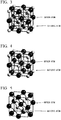
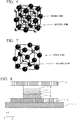
- FIG. 2 shows a structure of a spinel.
- a Sukenel structure referring to the spinel structure in which cations are disordered is a structure that has a lattice constant half the lattice constant of an ordered spinel structure while a position of an oxygen atom of the ordered spinel is almost not changed, and in which cations are positioned in tetrahedral positions and octahedral positions of oxygen atoms that are not occupied under ordinary circumstances.
- this structure may include total five structures shown in FIGS. 3 to 7 , and may be any one of them or a mixed structure thereof.
- the spinel structure in which cations are disordered may be referred to as a Sukenel structure.
- the Sukenel structure refers to a structure where oxygen atoms are arranged in cubic close-packed lattice that is substantially similar to spinel lattice, the structure as a whole belongs to a cubic structure, but arrangement of cations are disordered.
- Mg and Al are arranged in order in the tetrahedral vacancies and octahedral vacancies in the original spinel.
- the crystal symmetry of the structure is different from MgAl 2 O 4 , and the lattice constant of the structure is substantially half of that of MgAl 2 O 4 .
- the lattice-repeating unit With a change in the lattice-repeating unit, a combination between the ferromagnetic layer material and the electronic structure (band structure) is changed, and thus a large TMR enhancement due to a coherent tunneling effect is obtained.
- Non-Patent Document 2 a space group of MgAl 2 O 4 that is a non-magnetic spinel material is Fd-3m, but a space group of a disordered spinel structure with a lattice constant reduced by half is known to be changed to Fm-3m or F-43m, and there are total five structures (Non-Patent Document 2). Any one of them can be used.
- the Sukenel structure is not essentially required to be a cubic structure.
- the crystal structure is influenced by the crystal structure of the material of an underlayer, and the lattice is thus partially distorted.
- Each material has a bulk crystal structure, but in a case where it is formed into a thin film, a partially distorted crystal structure based on the bulk crystal structure can be taken.
- the tunnel barrier layer has a very thin structure, and is easily influenced by the crystal structure of the layer brought into contact with the tunnel barrier layer.
- the bulk crystal structure of a Sukenel structure is a cubic structure
- the Sukenel structure includes a Sukenel structure which does not have a cubic structure in addition to a Sukenel structure slightly deviating from the cubic structure.
- a deviation from the cubic structure in the Sukenel structure described in this specification is generally slight, and this deviation depends on the accuracy of a measurement method for evaluating the structure.
- a difference in ionic radius between the cations represented by M, Zn, Tl, and T2 contained in the tunnel barrier layer 3 is preferably 0.3 ⁇ or less.
- the difference in ionic radius is small, the cations are unlikely to be ordered, and thus the lattice constant becomes smaller than that of a general spinel structure. Accordingly, the MR ratio is further increased in a case where two or more types of elements that are similar to each other in ionic radius are combined.
- the tunnel barrier layer 3 preferably has a film thickness of 1.0 nm or greater. In a region where the film thickness of the tunnel barrier layer 3 is 1.0 nm or greater, the output voltage is constant. It can be thought that in a case where the film thickness of the tunnel barrier layer 3 is 1.0 nm or greater, a proportion of a current that flows and does not contribute to magnetoresistance is constant, and the output voltage is constant.
- the divalent cations in the elements contained in the tunnel barrier layer 3 are preferably zinc and any one of magnesium or cadmium.
- the cations are unlikely to be ordered, and thus the lattice constant becomes smaller than that of a general spinel structure. Accordingly, the MR ratio is further increased in a case where two or more types of elements that are similar to each other in ionic radius are combined.
- the divalent cations include plural types of elements such as magnesium, zinc, and cadmium, a spinel structure in which the cations are disordered is easily obtained.
- the trivalent cations in the elements contained in the tunnel barrier layer 3 are preferably aluminum and gallium.
- the difference in ionic radius is small, the cations are unlikely to be ordered, and thus the lattice constant becomes smaller than that of a general spinel structure. Accordingly, the MR ratio is further increased in a case where two or more types of elements that are similar to each other in ionic radius are combined.
- the trivalent cations are aluminum and gallium, a spinel structure in which the cations are disordered is easily obtained.
- the trivalent cations in the elements contained in the tunnel barrier layer 3 are preferably gallium and indium.
- the difference in ionic radius is small, the cations are unlikely to be ordered, and thus the lattice constant becomes smaller than that of a general spinel structure. Accordingly, the MR ratio is further increased in a case where two or more types of elements that are similar to each other in ionic radius are combined.
- the trivalent cations are gallium and indium, a spinel structure in which the cations are disordered is easily obtained.
- the number of elements of the divalent cation is preferably larger than half the number of elements of the trivalent cation. Disorder of cation sites is promoted, and the MR ratio is increased.
- Examples of the material of the first ferromagnetic metal layer 6 include metal selected from the group consisting of Cr, Mn, Co, Fe, and Ni, alloy including one or more of the metals of the group, and alloy including one or more metals selected from the group and at least one element of B, C, and N. Specific examples thereof include Co-Fe and Co-Fe-B.
- a Heusler alloy such as Co 2 FeSi is preferable in order to obtain a high output.
- the Heusler alloy includes intermetallic compounds having a chemical composition of X 2 YZ.
- X denotes a Co, Fe, Ni, or Cu group transition metal element or noble metal in the periodic table
- Y denotes a Mn, V, Cr, or Ti group transition metal, and can also take the elemental species of X
- Z denotes representative elements of III to V groups. Examples thereof include Co 2 FeSi, Co 2 MnSi, and Co 2 Mn 1-a Fe a Al b Si 1-b .
- an antiferromagnetic material such as IrMn and PtMn may be used as a material brought into contact with the first ferromagnetic metal layer 6 in order to make coercivity of the first ferromagnetic metal layer larger than that of the second ferromagnetic metal layer 7.
- the first ferromagnetic metal layer may have a synthetic ferromagnetic coupling structure such that the second ferromagnetic metal layer 7 is not influenced by a leakage magnetic field of the first ferromagnetic metal layer 6.
- a stacked film of Co and Pt is preferably used.
- the first ferromagnetic metal layer 6 has a composition of [Co (0.24 nm)/Pt (0.16 nm)] 6 /Ru (0.9 nm)/[Pt (0.16 nm)/Co (0.16 nm)] 4 /Ta (0.2 nm)/FeB (1.0 nm)
- the magnetization direction can be made perpendicular to the stacked plane.
- a ferromagnetic material particularly, a soft magnetic material is applied as a material of the second ferromagnetic metal layer 7, and examples thereof include metal selected from the group consisting of Cr, Mn, Co, Fe, and Ni, alloy including one or more of the metals of the group, and alloy including one or more metals selected from the group and at least one element of B, C, and N. Specific examples thereof include Co-Fe, Co-Fe-B, and Ni-Fe.
- the second ferromagnetic metal layer 7 preferably has a thickness of 2.5 nm or less. Perpendicular magnetic anisotropy can be applied to the second ferromagnetic metal layer 7 at an interface between the second ferromagnetic metal layer 7 and the tunnel barrier layer 3.
- the second ferromagnetic metal layer 7 preferably has a thin film thickness since the effect of the perpendicular magnetic anisotropy is reduced if the second ferromagnetic metal layer 7 has a thick film thickness.
- the first ferromagnetic metal layer 6 has a structure in which the magnetization direction thereof is fixed, and is called a fixed layer.
- the second ferromagnetic metal layer 7 has a magnetization direction that can be more easily changed by an external magnetic field or a spin torque than the first ferromagnetic metal layer 6, the second ferromagnetic metal layer is called a free layer.
- a magnetoresistance effect element according to the invention may be formed on a substrate.
- a material showing excellent flatness is preferably used as a material of the substrate 1.
- the substrate 1 differs depending on the purpose. For example, in a case of MRAM, a circuit formed in a Si substrate can be used under the magnetoresistance effect element. In a case of a magnetic head, an AlTiC substrate that can be easily processed can be used.
- an underlayer may be formed on the substrate.
- the underlayer 2 is used to control crystallinity such as crystal orientation and crystal grain size of the first ferromagnetic metal layer 6 and layers formed above the first ferromagnetic metal layer 6. Therefore, it is important to select the material of the underlayer 2.
- the material and the configuration of the underlayer 2 will be described. Any of a conductive material and an insulating material may be used for the underlayer, but in a case where electric power is fed to the underlayer, a conductive material is preferably used.
- a nitride layer having a (001)-oriented NaCl structure and containing at least one element selected from the group consisting of Ti, Zr, Nb, V, Hf, Ta, Mo, W, B, Al, and Ce is exemplified.
- a (002)-oriented perovskite conductive oxide layer made of RTO 3 is exemplified.
- the R-site includes at least one element selected from the group consisting of Sr, Ce, Dy, La, K, Ca, Na, Pb, and Ba
- the T-site includes at least one element selected from the group consisting of Ti, V, Cr, Mn, Fe, Co, Ni, Ga, Nb, Mo, Ru, Ir, Ta, Ce, and Pb.
- an oxide layer having a (001)-oriented NaCl structure and containing at least one element selected from the group consisting of Mg, Al, and Ce is exemplified.
- a layer having a (001)-oriented tetragonal or cubic structure and containing at least one element selected from the group consisting of Al, Cr, Fe, Co, Rh, Pd, Ag, Ir, Pt, Au, Mo, and W is exemplified.
- a layer having a stacked structure with a combination of two or more of the layers of the above first to fourth examples is exemplified.
- a cap layer may be formed on the second ferromagnetic metal layer of the magnetoresistance effect element according to the invention.
- a cap layer 4 is installed above the second ferromagnetic metal layer 7 in a stacking direction in order to control crystallinity such as crystal orientation and crystal grain size and element diffusion.
- the crystal structure of the cap layer may be any one of a fcc structure, a hcp structure, and a bcc structure.
- the crystal structure of the cap layer may be any one of a fcc structure, a hcp structure, and a bcc structure.
- the film thickness of the cap layer may be within such a range that a distortion relaxation effect is obtained and a reduction in the MR ratio by shunt is not shown.
- the film thickness of the cap layer is preferably 1 nm to 30 nm.
- a laminate formed of the first ferromagnetic metal layer, the tunnel barrier layer, and the second ferromagnetic metal layer 2 constituting the invention has a columnar shape.
- it may have various shapes such as a circular shape, a square shape, a triangle shape, and a polygonal shape when viewed from top, and preferably has a circular shape from the viewpoint of symmetry. That is, the laminate preferably has a columnar shape.
- FIGS. 8 and 9 show examples of the shape and the dimensions of the magnetoresistance effect element.
- FIG. 8 is a diagram showing a structure when viewed from a side in a stacking direction of the magnetoresistance effect element 100.
- the magnetoresistance effect element 100 of FIG. 8 has an electrode layer 5 formed above the cap layer 4 shown in FIG. 1 .
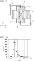
- FIG. 9 is a diagram showing a structure when viewed in the stacking direction of the magnetoresistance effect element 100. In FIG. 9 , a current source 71 and a voltmeter 72 are also shown.
- the magnetoresistance effect element 100 is processed into a columnar shape of 80 nm or less as shown in FIGS. 8 and 9 , and wiring is applied. Since the magnetoresistance effect element 100 is processed into a columnar shape having a size of 80 nm or less, a domain structure is not likely to be formed in the ferromagnetic metal layers, and it is not necessary to consider a component having a different spin polarization in the ferromagnetic metal layers. In FIG. 9 , the magnetoresistance effect element 100 is disposed at a position where the underlayer 2 and the electrode layer 5 intersect each other.
- the magnetoresistance effect element 100 can be evaluated with the structure shown in FIGS. 8 and 9 .
- the power supply 71 and the voltmeter 72 are disposed as shown in FIG. 9 such that a fixed current or a fixed voltage is applied to the magnetoresistance effect element 100.
- a change in the resistance of the magnetoresistance effect element 100 can be measured.
- MR Ratio % R AP ⁇ R P / R P ⁇ 100
- R P denotes a resistance in a case where magnetization directions of the first ferromagnetic metal layer 6 and the second ferromagnetic metal 7 are parallel to each other
- R AP denotes a resistance in a case where magnetization directions of the first ferromagnetic metal layer 6 and the second ferromagnetic metal 7 are antiparallel to each other.
- Jc inversion current value
- a stable output refers to the fact that the output voltage is in a range of (average output voltage ⁇ 2.5%) in a certain region.
- the tunnel barrier layer 7 of this application is used as an angle sensor, a difference of ⁇ 2.5% in output is acceptable in a case of reading an orientation with accuracy of 5 degrees.
- the structure has been exemplified in which the first ferromagnetic metal layer 6 having high coercivity is disposed on the lower side, but the invention is not limited to this structure.
- the coercivity is reduced in comparison with a case in which the first ferromagnetic metal layer 6 is disposed on the lower side, but the tunnel barrier layer 3 can be formed by utilizing the crystallinity of the substrate, and thus the MR ratio can be increased.
- a resistance change preferably changes linearly with respect to an external magnetic field.
- magnetization directions are easily directed into the stacking plane by shape anisotropy.
- a magnetic field is applied from outside to make the magnetization directions of the first ferromagnetic metal layer and the second ferromagnetic metal layer intersect each other, thereby changing the resistance change linearly with respect to the external magnetic field.
- a mechanism that applies a magnetic field is required near the magnetoresistance effect element, this is not preferable for integration.
- this is advantageous for integration since a method such as application of a magnetic field from outside is not required.
- the magnetoresistance effect element using this embodiment can be used as a magnetic sensor or a memory such as a MRAM Particularly, this embodiment is effective for products that are used with a bias voltage higher than a bias voltage used in conventional magnetic sensors.
- the magnetoresistance effect element 100 can be formed using, for example, a magnetron sputtering apparatus.
- the tunnel barrier layer 3 can be produced through a known method.
- a thin metal film is formed on the first ferromagnetic metal layer 6 by sputtering, performing plasma oxidation or natural oxidation by oxygen introduction thereon, and performing a heat treatment thereon.
- the film-forming method not only a magnetron sputtering method but also a thin film-forming method such as a vapor deposition method, a laser ablation method, or a MBE method can be used.
- Each of the underlayer, the first ferromagnetic metal layer, the second ferromagnetic metal layer, and the cap layer can be formed through a known method.
- a second embodiment is different from the first embodiment only in the method of forming a tunnel barrier layer.
- the tunnel barrier layer is formed by repeatedly performing formation and oxidation of a metal film.
- the substrate temperature is lowered to -70 to -30 degrees, and then oxidation is performed in the oxidation step.
- a temperature gradient is generated between the substrate and the vacuum or between the substrate and the plasma.
- epitaxial growth (lattice-matched growth) is easily adjusted. Since the crystal growth proceeds by the temperature gradient, the epitaxial growth is easily performed in a case where the temperature of the substrate is sufficiently lowered. As the temperature of the substrate is increased, domains are formed and a plurality of crystal nuclei are thus formed in the plane. Each of the crystal nuclei is independently and epitaxially grown, and thus a part in which lattices are not matched is formed in a part in which the grown domains are in contact with each other.
- the tunnel barrier layer lattice-matched parts, which are lattice-matched with both of a first ferromagnetic metal layer and a second ferromagnetic metal layer, partially exist.
- the tunnel barrier layer be completely lattice-matched to both of the first ferromagnetic metal layer and the second ferromagnetic metal layer.
- spin-polarized electrons interfere with each other during passing through the tunnel barrier layer, and thus the electrons do not easily pass through the tunnel barrier layer.
- the volume ratio of the lattice-matched part portion in the tunnel barrier layer with respect to the volume of the entire tunnel barrier layer is preferably 65% to 95%. In a case where the volume ratio of the lattice-matched part in the tunnel barrier layer is 65% or less, the effect of coherent tunneling is reduced, and thus the MR ratio decreases.
- the volume ratio of the lattice-matched part in the tunnel barrier layer is 95% or greater, the interference effect between the spin-polarized electrons during passing through the tunnel barrier layer is not be weakened, and thus an increase in passage of the spin-polarized electrons through the tunnel barrier layer is not observed.
- the volume ratio of the lattice-matched part (lattice-matched portion) with respect to the volume of the entire tunnel barrier layer can be estimated from, for example, a TEM image.
- a part including the tunnel barrier layer, the first ferromagnetic metal layer, and the second ferromagnetic metal layer in a cross-section TEM image is Fourier-transformed to obtain an electron beam diffraction image.
- electron beam diffraction image obtained by Fourier transformation electron beam diffraction spots in directions other than the stacking direction are removed. That image is subjected to inverse Fourier transformation to provide an image in which information only in the stacking direction is obtained.
- a part in which the tunnel barrier layer is continuously connected to both of the first ferromagnetic metal layer and the second ferromagnetic metal layer is defined as a lattice-matched portion.
- a part in which the tunnel barrier layer is not continuously connected to at least one of the first ferromagnetic metal layer and the second ferromagnetic metal layer, or in which no lattice lines are detected is defined as a lattice-mismatched portion.
- the layers are continuously connected from the first ferromagnetic metal layer to the second ferromagnetic metal layer via the tunnel barrier layer, and thus a width (L C ) of the lattice-matched portion can be measured from the TEM image.
- the layers are not continuously connected, and thus a width (L I ) of the lattice-mismatched portion can be measured from the TEM image.
- the volume ratio of the lattice-matched portion with respect to the volume of the entire tunnel barrier layer can be obtained.
- the TEM image is a cross-section image, but includes information including a depth. Accordingly, it can be thought that the region estimated from the TEM image is proportional to the volume.
- FIG. 23 shows an example of the part in which the tunnel barrier layer and the ferromagnetic metal layer are lattice-matched.
- FIG. 23(A) shows an example of a high-resolution cross-section TEM image.
- FIG. 23(B) shows an example of an image obtained by performing inverse Fourier transformation after removal of electron beam diffraction spots in directions other than the stacking direction in the electron beam diffraction image.
- components perpendicular to the stacking direction are removed, and thus lattice lines can be observed in the stacking direction. This shows that the tunnel barrier layer and the ferromagnetic metal layer are continuously connected to each other without interruption at an interface therebetween.
- Film formation was performed on a substrate provided with a thermal silicon oxide film using a magnetron sputtering method.
- As an underlayer 5 nm of Ta/3 nm of Ru was formed, and as a first ferromagnetic metal layer, 12 nm of IrMn/10 nm of CoFe/0.8 nm of Ru/7 nm of CoFe was formed in this order on the underlayer.
- a target having an alloy composition of Zn 0.7 Cd 0.25 Al 1.3 Ga 0.7 was subjected to sputtering to form a film with a thickness of t nm using a linear shutter. Thereafter, the above-described sample was moved to an oxidation chamber of which the inside was kept in an ultrahigh vacuum of 1 ⁇ 10 -8 Pa or less to perform natural oxidation by introducing Ar and oxygen.
- the natural oxidation time was 10 seconds
- the partial pressure ratio of Ar to oxygen was 1 to 30, and the total gas pressure was 0.1 Pa.
- a target having an alloy composition of Zn 0.7 Cd 0.25 Al 1.3 Ga 0.7 was subjected to sputtering to form a film with a thickness of t nm using a linear shutter.
- the above-described sample was moved to the oxidation chamber of which the inside was kept in an ultrahigh vacuum of 1 ⁇ 10 -8 Pa or less to perform natural oxidation and inductively coupled plasma oxidation by introducing Ar and oxygen.
- the natural oxidation time was 30 seconds, and the inductively coupled plasma oxidation time was 5 seconds.
- the partial pressure ratio of Ar to oxygen was 1 to 10, and the total gas pressure was 0.05 Pa.
- the above-described stacked film was installed in an annealing apparatus, and was heated at a temperature of 450°C in an Ar atmosphere for 10 minutes. Thereafter, under an applied field of 8 kOe, a heat treatment was performed on the stacked film at 280 degrees for 6 hours.
- a photoresist was formed using electron beam lithography in such a way that the electrode layer was in a direction rotated by 90 degrees as in FIG. 9 .
- a part other than a part below the photoresist was eliminated by an ion milling method to expose the thermal silicon oxide film that was the substrate, and thus a shape of the underlayer 2 was formed.
- a photoresist was formed into a cylindrical shape of 80 nm using electron beam lithography, and a part other than a part below the photoresist was eliminated by an ion milling method to expose the underlayer.
- SiOx was formed as an insulating layer on the part shaved by ion milling.
- the photoresist with a cylindrical shape of 80 nm was removed.
- the photoresist was not formed only in a part corresponding to an electrode pad of FIG. 9 , and the insulating layer was removed by an ion milling method to expose the underlayer.
- an Au layer was formed.
- This electrode pad 8 functions as a contact electrode for the underlayer of the above-described stacked film.
- a photoresist was formed and shaping was performed by an ion milling method such that the electrode layer of FIG. 9 was formed, and an Au film was formed. This functions as a contact electrode for the electrode layer of the above-described stacked film.
- the magnetoresistance element evaluation method is based on a magnetoresistance element evaluation method that has been generally performed. As shown in FIG. 9 , a current source and a voltmeter were connected to the electrode pad and the electrode layer, respectively, to perform measurement by a four-terminal method. 0.1 mA of a bias current was applied from an ammeter, and a voltage was measured by the voltmeter to obtain a resistance value. The changing resistance value was observed by applying a magnetic field to the magnetoresistance element from outside.
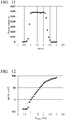
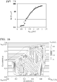
- FIG. 10 is a diagram showing a film thickness (2t) and a magnetoresistance (MR) ratio of the tunnel barrier layer of the magnetoresistance element of Example 1.
- FIG. 11 is a diagram showing a film thickness (2t) of the tunnel barrier layer of Example 1 and an output voltage obtained by the magnetoresistance effect. It is found that a region where the output voltage is stable is formed in a case where 2t is in the range of 1.0 to 2.1 nm. An output voltage ( ⁇ V) of the stable region of Example 1 is 58 mV.
- FIG. 12 is a diagram showing results of the evaluation of the area resistance (RA) of the magnetoresistance element of Example 1.
- the horizontal axis represents the film thickness (2t) of the tunnel barrier layer
- the vertical axis represents the RA. It is found that the RA is exponentially increased with an increase in the film thickness of the tunnel barrier layer. In addition, the RA is linearly increased in a case where 2t is 1.0 to 1.9 nm.
- the resistance of the tunnel barrier layer is known to be exponentially increased in proportion to an increase in the film thickness, and it is found that the region on the straight line is an optimum oxidation condition for the film thickness of the tunnel barrier layer produced in the example.
- the output voltage ( ⁇ V) of the stable region is 58 mV, and a region where the output voltage is stable is formed in a case where 2t is in the range of 1.0 to 2.1 nm.
- this film thickness region of the tunnel barrier layer is an optimum oxidation condition for the film thickness of the tunnel barrier layer.
- the composition of the tunnel barrier layer was analyzed using energy dispersive X-ray analysis (EDS).
- EDS energy dispersive X-ray analysis
- the content of B 3+ in a case where the tunnel barrier layer was expressed by a composition formula of AB 2 O 4 was defined as 2, and relative amounts of Zn and Cd were compared to each other.
- Quantitativity of O was ignored since it is difficult to perform quantitative evaluation of O. In general, the crystal structure can be maintained even in a case where the amount of O deviates from the quantitative ratio in an oxide.
- the production method is similar to that in Example 1, but only the material for forming the tunnel barrier layer is different.
- a target having an alloy composition of Mg 0.7 Zn 0.25 Al 1.3 Ga 0.7 was subjected to sputtering to form a film with a thickness of t nm using a linear shutter. Thereafter, the above-described sample was moved to an oxidation chamber of which the inside was kept in an ultrahigh vacuum of 1 ⁇ 10 -8 Pa or less to perform natural oxidation by introducing Ar and oxygen.
- the natural oxidation time was 10 seconds
- the division ratio of Ar to oxygen was 1 to 230
- the total gas pressure was 0.1 Pa.
- the sample was returned to a film forming chamber, and a target having an alloy composition of Mg 0.7 Zn 0.25 Al 1.3 Ga 0.7 was subjected to sputtering to form a film with a thickness of t nm using a linear shutter.
- the above-described sample was moved to the oxidation chamber of which the inside was kept in an ultrahigh vacuum of 1 ⁇ 10 -8 Pa or less to perform natural oxidation and inductively coupled plasma oxidation by introducing Ar and oxygen.
- the natural oxidation time was 30 seconds, and the inductively coupled plasma oxidation time was 5 seconds.
- the partial pressure ratio of Ar to oxygen was 1 to 10, and the total gas pressure was 0.05 Pa.
- the output voltage ( ⁇ V) of the stable region is 69 mV, and a region where the output voltage is stable is formed in a case where 2t is in the range of 1.1 to 1.9 nm.
- this film thickness region of the tunnel barrier layer is an optimum oxidation condition for the film thickness of the tunnel barrier layer.
- the tunnel barrier layer For structure analysis of the tunnel barrier layer, evaluation was performed with an electron diffraction image obtained using transmission electron beams. Through this method, the structure of the barrier layer was examined, and it was confirmed that there was no reflection from the ⁇ 022 ⁇ plane and the ⁇ 111 ⁇ plane shown in the ordered spinel structure. In addition, it was found that this barrier had a cubic structure in which the spinel structure was disordered.
- the composition of the tunnel barrier layer was analyzed using energy dispersive X-ray analysis (EDS).
- EDS energy dispersive X-ray analysis
- the content of B 3+ was defined as 2, and relative amounts of Mg and Zn were compared to each other.
- Quantitativity of O was ignored since it is difficult to perform quantitative evaluation of O.
- the crystal structure can be maintained even in a case where the amount of O deviates from the quantitative ratio in an oxide.
- the production method is similar to that in Example 1, but only the material for forming the tunnel barrier layer is different.
- a target having an alloy composition of Mg 0.7 Zn 0.25 Ga 0.7 In 0.3 was subjected to sputtering to form a film with a thickness of t nm using a linear shutter. Thereafter, the above-described sample was moved to an oxidation chamber of which the inside was kept in an ultrahigh vacuum of 1 ⁇ 10 -8 Pa or less to perform natural oxidation by introducing Ar and oxygen.
- the natural oxidation time was 10 seconds
- the partial pressure ratio of Ar to oxygen was 1 to 230
- the total gas pressure was 0.1 Pa.
- the sample was returned to a film forming chamber, and a target having an alloy composition of Mg 0.7 Zn 0.25 Ga 0.7 In 0.3 was subjected to sputtering to form a film with a thickness of t nm using a linear shutter.
- the above-described sample was moved to the oxidation chamber of which the inside was kept in an ultrahigh vacuum of 1 ⁇ 10 -8 Pa or less to perform natural oxidation and inductively coupled plasma oxidation by introducing Ar and oxygen.
- the natural oxidation time was 30 seconds, and the inductively coupled plasma oxidation time was 5 seconds.
- the partial pressure ratio of Ar to oxygen was 1 to 10, and the total gas pressure was 0.05 Pa.
- the output voltage ( ⁇ V) of the stable region is 43 mV, and a region where the output voltage is stable is formed in a case where 2t is in the range of 1.0 to 1.8 nm.
- this film thickness region of the tunnel barrier layer is an optimum oxidation condition for the film thickness of the tunnel barrier layer.
- the tunnel barrier layer For structure analysis of the tunnel barrier layer, evaluation was performed with an electron diffraction image obtained using transmission electron beams. Through this method, the structure of the barrier layer was examined, and it was confirmed that there was no reflection from the ⁇ 022 ⁇ plane and the ⁇ 111 ⁇ plane shown in the ordered spinel structure. In addition, it was found that this barrier had a cubic structure in which the spinel structure was disordered.
- the composition of the tunnel barrier layer was analyzed using energy dispersive X-ray analysis (EDS).
- EDS energy dispersive X-ray analysis
- the content of B 3+ was defined as 2, and relative amounts of Mg and Zn were compared to each other.
- Quantitativity of O was ignored since it is difficult to perform quantitative evaluation of O.
- the crystal structure can be maintained even in a case where the amount of O deviates from the quantitative ratio in an oxide.
- the production method is similar to that in Example 1, but only the material for forming the tunnel barrier layer is different.
- a target having an alloy composition of Zn 0.7 Cd 0.25 Ga 0.7 In 0.3 was subjected to sputtering to form a film with a thickness of t nm using a linear shutter. Thereafter, the above-described sample was moved to an oxidation chamber of which the inside was kept in an ultrahigh vacuum of 1 ⁇ 10 -8 Pa or less to perform natural oxidation by introducing Ar and oxygen.
- the natural oxidation time was 10 seconds
- the partial pressure ratio of Ar to oxygen was 1 to 230
- the total gas pressure was 0.1 Pa.
- the sample was returned to a film forming chamber, and a target having an alloy composition of Zn 0.7 Cd 0.25 Ga 0.7 In 0.3 was subjected to sputtering to form a film with a thickness of t nm using a linear shutter.
- the above-described sample was moved to the oxidation chamber of which the inside was kept in an ultrahigh vacuum of 1 ⁇ 10 -8 Pa or less to perform natural oxidation and inductively coupled plasma oxidation by introducing Ar and oxygen.
- the natural oxidation time was 30 seconds, and the inductively coupled plasma oxidation time was 5 seconds.
- the partial pressure ratio of Ar to oxygen was 1 to 10, and the total gas pressure was 0.05 Pa.
- the output voltage ( ⁇ V) of the stable region is 33 mV, and a region where the output voltage is stable is formed in a case where 2t is in the range of 1.3 to 1.8 nm.
- this film thickness region of the tunnel barrier layer is an optimum oxidation condition for the film thickness of the tunnel barrier layer.
- the tunnel barrier layer For structure analysis of the tunnel barrier layer, evaluation was performed with an electron diffraction image obtained using transmission electron beams. Through this method, the structure of the barrier layer was examined, and it was confirmed that there was no reflection from the ⁇ 022 ⁇ plane and the ⁇ 111 ⁇ plane shown in the ordered spinel structure. In addition, it was found that this barrier had a cubic structure in which the spinel structure was disordered.
- the composition of the tunnel barrier layer was analyzed using energy dispersive X-ray analysis (EDS).
- EDS energy dispersive X-ray analysis
- the content of B 3+ was defined as 2, and relative amounts of Zn and Cd were compared to each other.
- Quantitativity of O was ignored since it is difficult to perform quantitative evaluation of O.
- the crystal structure can be maintained even in a case where the amount of O deviates from the quantitative ratio in an oxide.
- the production method is similar to that in Example 1, but only the material for forming the tunnel barrier layer is different.
- a target having an alloy composition of Mg 0.83 Zn 0.43 Al 1.3 Ga 0.7 was subjected to sputtering to form a film with a thickness of t nm using a linear shutter. Thereafter, the above-described sample was moved to an oxidation chamber of which the inside was kept in an ultrahigh vacuum of 1 ⁇ 10 -8 Pa or less to perform natural oxidation by introducing Ar and oxygen.
- the natural oxidation time was 10 seconds
- the partial pressure ratio of Ar to oxygen was 1 to 230
- the total gas pressure was 0.1 Pa.
- the sample was returned to a film forming chamber, and a target having an alloy composition of Mg 0.83 Zn 0.43 Al 1.3 Ga 0.7 was subjected to sputtering to form a film with a thickness of t nm using a linear shutter.
- the above-described sample was moved to the oxidation chamber of which the inside was kept in an ultrahigh vacuum of 1 ⁇ 10 -8 Pa or less to perform natural oxidation and inductively coupled plasma oxidation by introducing Ar and oxygen.
- the natural oxidation time was 30 seconds, and the inductively coupled plasma oxidation time was 5 seconds.
- the partial pressure ratio of Ar to oxygen was 1 to 10, and the total gas pressure was 0.05 Pa.
- FIG. 13 is a diagram showing a film thickness (2t) and a magnetoresistance (MR) ratio of the tunnel barrier layer of the magnetoresistance element of Example 5. A maximum MR ratio is obtained in a case where 2t is 0.9 to 1.2 nm, and the MR ratio is reduced in a case where the film thickness of the tunnel barrier layer is greater than 1.2 nm.
- FIG. 14 is a diagram showing a film thickness (2t) of the tunnel barrier layer of Example 5 and an output voltage obtained by the magnetoresistance effect.
- FIG. 15 is a diagram showing results of the evaluation of the area resistance (RA) of the magnetoresistance element of Example 5.
- the horizontal axis represents the film thickness (2t) of the tunnel barrier layer, and the vertical axis represents the RA. It is found that the RA is exponentially increased with an increase in the film thickness of the tunnel barrier layer. In addition, the RA is linearly increased in a case where 2t is 1.1 to 2.0 nm.
- the resistance of the tunnel barrier layer is known to be exponentially increased in proportion to an increase in the film thickness, and it is found that the region on the straight line is an optimum oxidation condition for the film thickness of the tunnel barrier layer produced in the example. From the characteristic evaluation, it is found that the output voltage ( ⁇ V) of the stable region is 90 mV, and a region where the output voltage is stable is formed in a case where 2t is in the range of 1.2 to 1.7 nm. In addition, it is found that this film thickness region of the tunnel barrier layer is an optimum oxidation condition for the film thickness of the tunnel barrier layer.
- the tunnel barrier layer For structure analysis of the tunnel barrier layer, evaluation was performed with an electron diffraction image obtained using transmission electron beams. Through this method, the structure of the barrier layer was examined, and it was confirmed that there was no reflection from the ⁇ 022 ⁇ plane and the ⁇ 111 ⁇ plane shown in the ordered spinel structure. In addition, it was found that this barrier had a cubic structure in which the spinel structure was disordered.
- the composition of the tunnel barrier layer was analyzed using energy dispersive X-ray analysis (EDS).
- EDS energy dispersive X-ray analysis
- the content of B 3+ was defined as 2, and relative amounts of Mg and Zn were compared to each other.
- Quantitativity of O was ignored since it is difficult to perform quantitative evaluation of O.
- the crystal structure can be maintained even in a case where the amount of O deviates from the quantitative ratio in an oxide.
- the production method is similar to that in Example 1, but only the material for forming the tunnel barrier layer is different.
- Mg, Zn, Al, and Ga targets were simultaneously subjected to sputtering to form a film with a thickness of t nm using a linear shutter such that an arbitrary composition ratio is obtained.
- the sum of the contents of Mg and Zn was adjusted so as to be 45% of the sum of the contents of Al and Ga in terms of composition ratio.
- the above-described sample was moved to an oxidation chamber of which the inside was kept in an ultrahigh vacuum of 1 ⁇ 10 -8 Pa or less to perform natural oxidation by introducing Ar and oxygen.
- the natural oxidation time was 10 seconds, the partial pressure ratio of Ar to oxygen was 1 to 23, and the total gas pressure was 0.1 Pa. Then, the sample was returned to a film forming chamber, and Mg, Zn, Al, and Ga targets were simultaneously subjected to sputtering to form a film with a thickness of t nm using a linear shutter such that an arbitrary composition ratio is obtained. At this time, the sum of the contents of Mg and Zn was adjusted so as to be 45% of the sum of the contents of Al and Ga in terms of composition ratio.
- the above-described sample was moved to the oxidation chamber of which the inside was kept in an ultrahigh vacuum of 1 ⁇ 10 -8 Pa or less to perform natural oxidation and inductively coupled plasma oxidation by introducing Ar and oxygen.
- the natural oxidation time was 30 seconds, and the inductively coupled plasma oxidation time was 5 seconds.
- the partial pressure ratio of Ar to oxygen was 1 to 10, and the total gas pressure was 0.05 Pa.
- the tunnel barrier layer For structure analysis of the tunnel barrier layer, evaluation was performed with an electron diffraction image obtained using transmission electron beams. Through this method, the structure of the barrier layer was examined, and it was confirmed that there was no reflection from the ⁇ 022 ⁇ plane and the ⁇ 111 ⁇ plane shown in the ordered spinel structure. In addition, it was found that this barrier had a cubic structure in which the spinel structure was disordered.
- the composition of the tunnel barrier layer was analyzed using energy dispersive X-ray analysis (EDS).
- EDS energy dispersive X-ray analysis
- the content of B 3+ was defined as 2, and relative amounts of Mg and Zn were compared to each other.
- Quantitativity of O was ignored since it is difficult to perform quantitative evaluation of O. In general, the crystal structure can be maintained even in a case where the amount of O deviates from the quantitative ratio in an oxide.
- FIG. 16 is a three-dimensional diagram of a range of a film thickness at which an output voltage independent of the film thickness is obtained in a case where the tunnel barrier layer of Example 6 has a composition ratio of (Mg 1-x Zn x ) 0.9 (Al 2-y Ga y )O 4 . That is, FIG. 16 is a diagram in which the horizontal axis x represents a composition ratio of an A 2+ site, the vertical axis y represents a composition ratio of a B 3+ site, and the Z-axis direction represents a width (nm) of the film thickness at which the output voltage is independent of the film thickness. Patterns outside the right frame in FIG. 16 will be described.
- the horizontal stripe pattern represents a voltage of 0 V to less than 0.4 V
- the narrow vertical stripe pattern represents a voltage of 0.4 V to less than 0.6 V
- the oblique stripe pattern represents a voltage of 0.6 V to less than 0.8 V
- the wide vertical stripe pattern represents a voltage of 0. V or greater.
- the wide vertical stripe pattern indicates that a voltage of a region where the voltage is stable is 0.8 V or greater
- the horizontal stripe pattern indicates that a voltage of a region where the voltage is stable is less than 0.4 V.
- the production method is similar to that in Example 1, but only the method for forming the tunnel barrier layer is different.
- a film was formed on a substrate provided with a thermal silicon oxide film using a magnetron sputtering method. 5 nm of Ta/3 nm of Ru was formed as an underlayer, and 12 nm of IrMn/10 nm of CoFe/0.8 nm of Ru/7 nm of CoFe was formed as a first ferromagnetic metal layer in order.
- a method of forming a tunnel barrier layer will be shown.
- 0.8 nm of Zn 0.7 Cd 0.25 Al 1.3 Ga 0.7 was formed by sputtering.
- the above-described sample was moved to an oxidation chamber of which the inside was kept in an ultrahigh vacuum of 1 ⁇ 10 -8 Pa or less, and the substrate was cooled to -70 to -30 degrees. Then, natural oxidation was performed by introducing Ar and oxygen. The natural oxidation time was 10 seconds, the partial pressure ratio of Ar to oxygen was 1 to 30, and the total gas pressure was 0.1 Pa. Then, the sample was returned to a film forming chamber, and 0.6 nm of Zn 0.7 Cd 0.25 Al 1.3 Ga 0.7 was formed by sputtering.
- the above-described sample was moved to the oxidation chamber of which the inside was kept in an ultrahigh vacuum of 1 ⁇ 10 -8 Pa or less, and the substrate was cooled to -70 to -30 degrees. Then, natural oxidation and inductively coupled plasma oxidation were performed by introducing Ar and oxygen.
- the natural oxidation time was 30 seconds, and the inductively coupled plasma oxidation time was 5 seconds.
- the partial pressure ratio of Ar to oxygen was 1 to 10, and the total gas pressure was 0.05 Pa.
- a volume ratio of the lattice-matched part (lattice-matched portion) with respect to the volume of the entire tunnel barrier layer was calculated as described above using a cross-section transmission electron microscope (TEM) image and an image obtained by removing electron beam diffraction spots in a direction other than a stacking direction in an electron beam diffraction image obtained by Fourier-transforming the TEM image and by then performing inverse Fourier transformation.
- TEM transmission electron microscope
- FIG. 24 is a structural schematic diagram of a cross-section including a direction parallel to the stacking direction of Example 7. From the high-resolution cross-section TEM image obtained in Example 7, it was found that a size (width) of the film surface of the lattice-matched part of the tunnel barrier layer in a direction parallel thereto was 30 nm or less in any part. 30 nm is about 10 times the lattice constant of the CoFe alloy that is the material of the first ferromagnetic metal layer and the second ferromagnetic metal layer, and mutual interference of the spin-polarized electrons in a direction perpendicular to the tunneling direction before or after coherent tunneling can be thought to be intensified about 10 times the lattice constant.
- FIG. 25 is a diagram showing a volume ratio of the lattice-matched part (lattice-matched portion) with respect to the volume of the entire tunnel barrier layer of Example 7 and characteristics of the element.
- FIG. 25(A) is a diagram showing element resistance (Rp) when magnetization directions of the first ferromagnetic metal layer and the second ferromagnetic metal layer are parallel to each other.
- FIG. 25(B) is a diagram showing element resistance (Rap) when magnetization directions of the first ferromagnetic metal layer and the second ferromagnetic metal layer are antiparallel to each other.
- FIG. 25(C) is a diagram showing a magnetoresistance ratio of the element.
- the Rp tends to be reduced when the proportion of the lattice-matched part in which the tunnel barrier layer is lattice-matched to both of the first ferromagnetic metal layer and the second ferromagnetic metal layer is in the range of 65% to 95%. Regarding this, in a case where the tunnel barrier layer is completely lattice-matched, spin-polarized electrons interfere with each other during passing through the tunnel barrier layer, and thus it is thought that the electrons do not easily pass through the tunnel barrier layer.
- the production method is similar to that in Example 1, but only the material for forming the tunnel barrier layer is different.
- a Mg target was subjected to sputtering to form a film with a thickness of t nm using a linear shutter. Thereafter, the above-described sample was moved to an oxidation chamber of which the inside was kept in an ultrahigh vacuum of 1 ⁇ 10 -8 Pa or less to perform natural oxidation by introducing Ar and oxygen.
- the natural oxidation time was 10 seconds
- the partial pressure ratio of Ar to oxygen was 1 to 30, and the total gas pressure was 0.1 Pa.
- the sample was returned to a film forming chamber, and a Mg target was subjected to sputtering to form a film with a thickness of t nm using a linear shutter.
- the above-described sample was moved to the oxidation chamber of which the inside was kept in an ultrahigh vacuum of 1 ⁇ 10 -8 Pa or less to perform natural oxidation and inductively coupled plasma oxidation by introducing Ar and oxygen.
- the natural oxidation time was 30 seconds, and the inductively coupled plasma oxidation time was 5 seconds.
- the partial pressure ratio of Ar to oxygen was 1 to 10, and the total gas pressure was 0.05 Pa.
- FIG. 17 is a diagram showing a film thickness (2t) and a magnetoresistance (MR) ratio of the tunnel barrier layer of the magnetoresistance element of Comparative Example 1.
- a maximum MR ratio is obtained in a case where 2t is 1.24 to 1.82 nm, and the MR ratio is reduced in a case where the film thickness of the tunnel barrier layer is greater than 1.82 nm.
- FIG. 18 is a diagram showing a film thickness (2t) of the tunnel barrier layer of Comparative Example 1 and an output voltage obtained by the magnetoresistance effect. A maximum output voltage is obtained in a case where 2t is 2.0 nm.
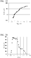
- FIG. 19 is a diagram showing results of the evaluation of the area resistance (RA) of the magnetoresistance element of Comparative Example 1.
- the horizontal axis represents the film thickness (2t) of the tunnel barrier layer, and the vertical axis represents the RA.
- RA area resistance
- the resistance of the tunnel barrier layer is known to be exponentially increased in proportion to an increase in the film thickness, and it is found that the region on the straight line is an optimum oxidation condition for the film thickness of the tunnel barrier layer produced in the example.
- the production method is similar to that in Example 1, but only the material for forming the tunnel barrier layer is different.
- a MgIn 2 target was subjected to sputtering to form a film with a thickness of t nm using a linear shutter. Thereafter, the above-described sample was moved to an oxidation chamber of which the inside was kept in an ultrahigh vacuum of 1 ⁇ 10 -8 Pa or less to perform natural oxidation by introducing Ar and oxygen.
- the natural oxidation time was 10 seconds
- the partial pressure ratio of Ar to oxygen was 1 to 30, and the total gas pressure was 0.1 Pa.
- the sample was returned to a film forming chamber, and a MgIn 2 target was subjected to sputtering to form a film with a thickness of t nm using a linear shutter.
- the above-described sample was moved to the oxidation chamber of which the inside was kept in an ultrahigh vacuum of 1 ⁇ 10 -8 Pa or less to perform natural oxidation and inductively coupled plasma oxidation by introducing Ar and oxygen.
- the natural oxidation time was 30 seconds, and the inductively coupled plasma oxidation time was 5 seconds.
- the partial pressure ratio of Ar to oxygen was 1 to 10, and the total gas pressure was 0.05 Pa.
- FIG. 20 is a diagram showing a film thickness (2t) and a magnetoresistance (MR) ratio of the tunnel barrier layer of the magnetoresistance element of Comparative Example 2. A maximum MR ratio is obtained in a case where 2t is 0.8 to 1.46 nm, and the MR ratio is reduced in a case where the film thickness of the tunnel barrier layer is greater than 1.46 nm.
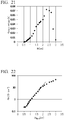
- FIG. 21 is a diagram showing a film thickness (2t) of the tunnel barrier layer of Comparative Example 2 and an output voltage obtained by the magnetoresistance effect. A maximum output voltage is obtained in a case where 2t is 2.28 nm.
- FIG. 22 is a diagram showing results of the evaluation of the area resistance (RA) of the magnetoresistance element of Comparative Example 2.
- the horizontal axis represents the film thickness (2t) of the tunnel barrier layer, and the vertical axis represents the RA.
- RA area resistance
- 2t the film thickness of the tunnel barrier layer
- RA is linearly increased in a case where 2t is 0.9 to 1.84 m.
- the resistance of the tunnel barrier layer is known to be exponentially increased in proportion to an increase in the film thickness, and it is found that the region on the straight line is an optimum oxidation condition for the film thickness of the tunnel barrier layer produced in the example.
- the tunnel barrier layer For structure analysis of the tunnel barrier layer, evaluation was performed with an electron diffraction image obtained using transmission electron beams. Through this method, the structure of the barrier layer was examined, and it was confirmed that there was no reflection from the ⁇ 022 ⁇ plane and the ⁇ 111 ⁇ plane shown in the ordered spinel structure. In addition, it was found that this barrier had a spinel structure.
- the composition of the tunnel barrier layer was analyzed using energy dispersive X-ray analysis (EDS).
- EDS energy dispersive X-ray analysis
- the content of B 3+ was defined as 2, and relative amounts of Mg and Zn were compared to each other.
- Quantitativity of O was ignored since it is difficult to perform quantitative evaluation of O. In general, the crystal structure can be maintained even in a case where the amount of O deviates from the quantitative ratio in an oxide.
- the production method is similar to that in Example 1, but only the material for forming the tunnel barrier layer is different.
- a Mg 0.7 Zn 0.25 Al 2 target was subjected to sputtering to form a film with a thickness of t nm using a linear shutter. Thereafter, the above-described sample was moved to an oxidation chamber of which the inside was kept in an ultrahigh vacuum of 1 ⁇ 10 -8 Pa or less to perform natural oxidation by introducing Ar and oxygen.
- the natural oxidation time was 10 seconds
- the partial pressure ratio of Ar to oxygen was 1 to 30, and the total gas pressure was 0.1 Pa.
- the sample was returned to a film forming chamber, and a Mg 0.7 Zn 0.25 Al 2 target was subjected to sputtering to form a film with a thickness of t nm using a linear shutter.
- the above-described sample was moved to the oxidation chamber of which the inside was kept in an ultrahigh vacuum of 1 ⁇ 10 -8 Pa or less to perform natural oxidation and inductively coupled plasma oxidation by introducing Ar and oxygen.
- the natural oxidation time was 30 seconds, and the inductively coupled plasma oxidation time was 5 seconds.
- the partial pressure ratio of Ar to oxygen was 1 to 10, and the total gas pressure was 0.05 Pa.
- 0.1 mA of a bias current was applied from an ammeter, and a voltage was measured by a voltmeter to obtain a resistance value.
- a maximum MR ratio is obtained in a case where 2t is 0.9 to 1.4 nm, and the MR ratio is reduced in a case where the film thickness of the tunnel barrier layer is greater than 1.4 nm.
- a maximum output voltage is obtained in a case where 2t is 1.6 nm. The region where the output voltage was stable, observed in Examples 1 to 6, was not observed.
- the RA is linearly increased in a case where 2t is 0.8 to 2.0 m.
- the resistance of the tunnel barrier layer is known to be exponentially increased in proportion to an increase in the film thickness, and it is found that the region on the straight line is an optimum oxidation condition for the film thickness of the tunnel barrier layer produced in the example.
- the production method is similar to that in Example 1, but only the material for forming the tunnel barrier layer is different.
- a target having an alloy composition of Mg 0.7 Pb 0.25 Al 1.3 Ga 0.7 was subjected to sputtering to form a film with a thickness of t nm using a linear shutter. Thereafter, the above-described sample was moved to an oxidation chamber of which the inside was kept in an ultrahigh vacuum of 1 ⁇ 10 -8 Pa or less to perform natural oxidation by introducing Ar and oxygen.
- the natural oxidation time was 10 seconds
- the partial pressure ratio of Ar to oxygen was 1 to 230
- the total gas pressure was 0.1 Pa.
- the sample was returned to a film forming chamber, and a target having an alloy composition of Mg 0.7 Pb 0.25 Al 1.3 Ga 0.7 was subjected to sputtering to form a film with a thickness of t nm using a linear shutter.
- the above-described sample was moved to the oxidation chamber of which the inside was kept in an ultrahigh vacuum of 1 ⁇ 10 -8 Pa or less to perform natural oxidation and inductively coupled plasma oxidation by introducing Ar and oxygen.
- the natural oxidation time was 30 seconds, and the inductively coupled plasma oxidation time was 5 seconds.
- the partial pressure ratio of Ar to oxygen was 1 to 10, and the total gas pressure was 0.05 Pa.
- the output voltage ( ⁇ V) of the stable region is 10 mV, and a region where the output voltage is stable is not formed at any film thickness.
- this film thickness region of the tunnel barrier layer is an optimum oxidation condition for the film thickness of the tunnel barrier layer.
- the tunnel barrier layer For structure analysis of the tunnel barrier layer, evaluation was performed with an electron diffraction image obtained using transmission electron beams. Through this method, the structure of the barrier layer was examined, and it was confirmed that there was no reflection from the ⁇ 022 ⁇ plane and the ⁇ 111 ⁇ plane shown in the ordered spinel structure. In addition, it was found that this barrier had a cubic structure in which the spinel structure was disordered.
- the composition of the tunnel barrier layer was analyzed using energy dispersive X-ray analysis (EDS).
- EDS energy dispersive X-ray analysis
- the content of B 3+ was defined as 2, and relative amounts of Mg and Zn were compared to each other.
- Quantitativity of O was ignored since it is difficult to perform quantitative evaluation of O.
- the crystal structure can be maintained even in a case where the amount of O deviates from the quantitative ratio in an oxide.
- Table 1 shows the examples and the comparative examples. [Table 1] EXAMPLES 2t @ ⁇ V [nm] ⁇ V [mV] EXAMPLE 1 1.0 ⁇ 2.1 58 EXAMPLE 2 1.1 ⁇ 1.9 69 EXAMPLE 3 1.0-1.8 43 EXAMPLE 4 1.3 ⁇ 1.8 33 EXAMPLE 5 1.2 ⁇ 1.7 90
- the output voltage ( ⁇ V) of the stable region was not observed under the conditions of the comparative examples from the characteristic evaluation.
- the output voltage of the stable region is observed in a film thickness region of the tunnel barrier layer having a thickness of at least 1.0 nm or greater.
- the examples have a more optimum condition.
- the condition is that the difference in ionic radius between the cations contained in the tunnel barrier layer is 0.3 ⁇ or less.
- Table 2 shows ionic radiuses of the cations used in the examples and the comparative examples.
- Table 3 shows a difference between the maximum ionic radius and the minimum ionic radius of the cations obtained from Table 2, and a width (2tw) of the film thickness region of the tunnel barrier layer in which an output voltage of the stable region is obtained in each of the examples.
- the width of the film thickness region of the tunnel barrier layer is 0.5 nm or greater.
- the invention can be applied to a magnetoresistance effect element capable of obtaining an output voltage independent of a film thickness of a tunnel barrier layer.
Landscapes
- Engineering & Computer Science (AREA)
- Power Engineering (AREA)
- Physics & Mathematics (AREA)
- Manufacturing & Machinery (AREA)
- Chemical & Material Sciences (AREA)
- Crystallography & Structural Chemistry (AREA)
- Condensed Matter Physics & Semiconductors (AREA)
- General Physics & Mathematics (AREA)
- Computer Hardware Design (AREA)
- Hall/Mr Elements (AREA)
- Mram Or Spin Memory Techniques (AREA)
Abstract
Description
- The present invention relates to a magnetoresistance effect element.
- Priority is claimed on Japanese Patent Application No.
2015-071413, filed on March 31, 2015 - Giant magnetoresistance (GMR) elements formed of a multilayer film consisting of a ferromagnetic layer and a non-magnetic layer, and tunnel magnetoresistance (TMR) elements using an insulating layer (a tunnel barrier layer or a barrier layer) as a non-magnetic layer have been known. In general, TMR elements have higher element resistance than GMR elements, but a magnetoresistance (MR) ratio of the TMR elements is higher than that of the GMR elements. The TMR elements can be divided into two types. One type is related to TMR elements using only a tunneling effect using an effect of soaking-out of a wave function between ferromagnetic layers. The other type is related to TMR elements using coherent tunneling using conduction in a specific orbit of a non-magnetic insulating layer where tunneling is carried out when the above-described tunneling effect is caused. TMR elements using coherent tunneling have been known to obtain a higher MR ratio than TMR elements using only tunneling. The coherent tunneling effect is caused in a case where both of the ferromagnetic layer and the non-magnetic insulating layer are crystalline and an interface between the ferromagnetic layer and the non-magnetic insulating layer is crystallographically continuous.
- Magnetoresistance effect elements are used for various purposes. For example, magnetoresistance effect-type magnetic sensors have been known as magnetic sensors, and magnetoresistance effect elements determine characteristics of a reproducing function of hard disk drives. Magnetic sensors have a system that detects, as a resistance change of a magnetoresistance effect element, an effect that a magnetization direction of the magnetoresistance effect element is changed by an external magnetic field. Highly anticipated devices are magnetoresistance change-type random access memories (MRAM). MRAMs are memories that read magnetoresistance as digital signals of 0 and 1 by appropriately changing ferromagnetic magnetization directions of two layers to parallel or antiparallel directions.
-
- [Patent Document 1] Japanese Patent No.
5586028 - [Patent Document 2] Japanese Unexamined Patent Application, First Publication No.
2013-175615 -
- [Non-Patent Document 1] Hiroaki Sukegawa, a [1] Huixin Xiu, Tadakatsu Ohkubo, Takao Furubayashi, Tomohiko Niizeki, Wenhong Wang, Shinya Kasai, Seiji Mitani, Koichiro Inomata, and Kazuhiro Hono, APPLIED PHYSICS LETTERS 96, 212505 [1] (2010)
- [Non-Patent Document 2] Thomas Scheike, Hiroaki Sukegawa, Takao Furubayashi, Zhenchao Wen, Koichiro Inomata, Tadakatsu Ohkubo, Kazuhiro Hono, and Seiji Mitani, Applied Physics Letters, 105,242407 (2014)
- [Non-Patent Document 3] Yoshio Miura, Shingo Muramoto, Kazutaka Abe, and Masafumi Shirai, Physical Review B 86, 024426 (2012)
- In recent years, it has been required to use MgO or MgAl2O4 as a non-magnetic insulating layer in order to cause the coherent tunneling. It has been reported that depending on the production method, MgO or MgAl2O4 exhibits a maximum MR ratio at a specific film thickness and the MR ratio is gradually reduced at a film thickness exceeding the above specific film thickness. That is, the tunnel barrier layer is very sensitive to the film thickness, and it was difficult to produce magnetoresistance elements capable of obtaining a constant output voltage in a large amount of elements. Therefore, in a case where magnetoresistance effect elements are applied to magnetic sensors and the like, it is required to correct an output for each produced element.
- Future devices such as magnetic sensors and MRAMs are required to obtain a sufficiently high MR ratio even at a high bias voltage. In a magnetic sensor, an electrical signal obtained as a resistance change in a circuit should be amplified in order to observe a minute magnetic field such as geomagnetism or biomagnetism. In order to realize higher sensitivity than conventional sensors, as well as the MR ratio, an output voltage or an output current is also required to be increased, and driving at a high bias voltage is also required. In a case of MRAM, high-voltage driving is required in a write operation. In spin transfer torque-type (STT) MRAMs, the more the magnetization direction of a ferromagnetic layer changes, the higher current density is required to be applied to the magnetoresistance effect element. The magnetization direction of a ferromagnetic layer is an effect of the action of a spin-polarized current on the spin of the ferromagnetic layer. Similarly to the MR ratio, a rewrite current is generated by a strong spin-polarized current, and thus a high MR ratio is similarly required at a high bias voltage in STT-MRAMs.
- In
Patent Document 1 andNon-Patent Document 1, a tunnel barrier having a spinel structure is reported to be effective as a substituent material for MgO. A spinel tunnel barrier expressed by a composition formula of MgAl2O4 has been known to obtain the same MgO ratio as MgO, and to obtain a higher MR ratio than MgO at a high bias voltage. In addition, inPatent Document 2 andNon-Patent Documents - The invention is contrived in view of the above-described circumstances, and an object thereof is to provide a magnetoresistance effect element capable of obtaining an output voltage independent of a film thickness of a tunnel barrier layer.
- In order to solve the above-described problems, a magnetoresistance effect element has a first ferromagnetic metal layer, a second ferromagnetic metal layer, and a tunnel barrier layer that is sandwiched between the first and second ferromagnetic metal layers, the tunnel barrier layer has a spinel structure in which cations are arranged in a disordered manner, and the tunnel barrier layer is expressed by a composition formula of (M1-xZnx)((T1)2-y(T2)y)O4 wherein M represents a non-magnetic divalent cation other than Zn, each of T1 and T2 represents a non-magnetic trivalent cation, and x and y represent a composition ratio in a region where composition ratios combined as follows ((1) to (5)) are vertexes, and the vertexes are connected by straight lines;
- (1) x=0.2, y=0.1,
- (2) x=0. 8, y=0.1,
- (3) x=0.8, y=1.7,
- (4) x=0.6, y=1.7, and
- (5) x=0.2, y=0.7.
- In the magnetoresistance effect element, the tunnel barrier layer has a spinel structure in which cations are arranged in a disordered manner. In a case where a different non-magnetic element is disposed in a cation site of the spinel structure of the tunnel barrier layer, the basic lattice constant is half the lattice constant of a conventional spinel structure, and the MR ratio is increased. In addition, by substitution of plural cations, an impurity level is formed in an energy gap, and when a certain voltage is applied to the element, conduction via the impurity level is caused. Therefore, the output voltage in magnetoresistance is not increased. As a result, a region where the output voltage is stable is formed.
- In the magnetoresistance effect element, the tunnel barrier layer may have a lattice-matched portion that is lattice-matched with both of the first ferromagnetic metal layer and the second ferromagnetic metal layer, and a lattice-mismatched portion that is not lattice-matched with at least one of the first ferromagnetic metal layer and the second ferromagnetic metal layer.
- In the magnetoresistance effect element, a volume ratio of the lattice-matched portion in the tunnel barrier layer with respect to a volume of the entire tunnel barrier layer may be 65% to 95%.
- In a case where the volume ratio of the lattice-matched portion in the tunnel barrier layer is 65% or less, the effect of coherent tunneling decreases, and thus the MR ratio is reduced. In a case where the volume ratio of the lattice-matched portion in the tunnel barrier layer is 95% or greater, the interference effect between the spin-polarized electrons during passing through the tunnel barrier layer does not decrease, and thus an increase in passage of the spin-polarized electrons through the tunnel barrier layer is not observed. By making the number of constituent elements of the non-magnetic element smaller than half the number of elements of the aluminum ion, vacancies are generated in the cation sites, the vacancies and two or more types of non-magnetic elements occupy the cations sites, and thus lattice periodicity is disturbed. Accordingly, the MR ratio is further increased.
- In the magnetoresistance effect element, in the composition formula, a difference in ionic radius between the cations represented by M, Zn, T1, and T2 may be 0.3 Å or less. That is, in a case where ionic radiuses of two cations among M, Zn, T1, and T2 are compared to each other, a difference therebetween may be 0.3 Å or less. In a case where the difference in ionic radius is small, the cations are unlikely to be ordered, and thus the lattice constant becomes smaller than that of a general spinel structure. Accordingly, the MR ratio is further increased in a case where two or more types of elements that are similar to each other in ionic radius are combined. In addition, the film thickness at which a region at which the output voltage is stable is formed is increased.
- In the magnetoresistance effect element, in the composition formula, M may represent a cation of magnesium or cadmium. In a case where the difference in ionic radius is small, the cations are unlikely to be ordered, and thus the lattice constant becomes smaller than that of a general spinel structure. Accordingly, the MR ratio is further increased in a case where two or more types of elements that are similar to each other in ionic radius are combined. Particularly, in a case where the divalent cation includes a cation of magnesium or cadmium, a spinel structure in which the cations are disordered is easily obtained.
- In the magnetoresistance effect element, in the composition formula, one of T1 and T2 may represent a cation of aluminum, and the other may represent a cation of gallium. In a case where the difference in ionic radius is small, the cations are unlikely to be ordered, and thus the lattice constant becomes smaller than that of a general spinel structure. Accordingly, the MR ratio is further increased in a case where two or more types of elements that are similar to each other in ionic radius are combined. Particularly, in a case where the trivalent cations are aluminum and gallium, a spinel structure in which the cations are disordered is easily obtained.
- In the magnetoresistance effect element, in the composition formula, one of T1 and T2 may represent a cation of gallium, and the other may represent a cation of indium. In a case where the difference in ionic radius is small, the cations are unlikely to be ordered, and thus the lattice constant becomes smaller than that of a general spinel structure. Accordingly, the MR ratio is further increased in a case where two or more types of elements that are similar to each other in ionic radius are combined.
- In the magnetoresistance effect element, in the tunnel barrier layer, the number of elements of the divalent cation may be smaller than half the number of elements of the trivalent cation. Disorder of cation sites is promoted, and the MR ratio is increased.
- In the magnetoresistance effect element, at least one of the first ferromagnetic metal layer and the second ferromagnetic metal layer may be Co2Mn1-aFeaAlbSi1-b (0≤a≤1, 0≤b≤1). Co2Mn1-aFeaAlbSi1-b is a ferromagnetic metal material having high spin polarizability, and a higher MR ratio can be obtained than in a case where another ferromagnetic metal material is used.
- In the magnetoresistance effect element, a film thickness of the tunnel barrier layer may be 1.0 nm or greater. In a region where the film thickness of the tunnel barrier layer is 1.0 nm or greater, the output voltage is constant. It can be thought that in a case where the film thickness of the tunnel barrier layer is 1.0 nm or greater, a proportion of a current that flows and does not contribute to magnetoresistance is constant, and the output voltage is constant.
- In the magnetoresistance effect element, the first ferromagnetic metal layer may have larger coercivity than the second ferromagnetic metal layer. Since the coercivity of the first ferromagnetic metal layer is different from that of the second ferromagnetic metal layer, the element functions as a spin valve, and device application is possible.
- In the magnetoresistance effect element, at least one of the first ferromagnetic metal layer and the second ferromagnetic metal layer may have magnetic anisotropy perpendicular to a stacking direction. Since it is not necessary to apply a bias magnetic field in a case where the element is used in a MRAM or a high-frequency device, it is possible to reduce the device in size. In addition, the element can be allowed to function as a recording element since it has high thermal disturbance resistance.
- According to the invention, it is possible to provide a magnetoresistance effect element capable of obtaining an output voltage independent of a film thickness of a tunnel barrier layer.
-
-
FIG. 1 shows a stacked structure of a magnetoresistance effect element. -
FIG. 2 is a diagram of a crystal structure of a spinel. -
FIG. 3 is a schematic diagram of an ordered spinel structure and a disordered spinel structure with symmetry of Fm-3m having a lattice constant assumed in a tunnel barrier layer of the invention. -
FIG. 4 is a schematic diagram of an ordered spinel structure and a disordered spinel structure with symmetry of Fm-3m having a lattice constant assumed in a tunnel barrier layer of the invention. -
FIG. 5 is a schematic diagram of an ordered spinel structure and a disordered spinel structure with symmetry of Fm-3m having a lattice constant assumed in a tunnel barrier layer of the invention. -
FIG. 6 is a schematic diagram of an ordered spinel structure and a disordered spinel structure with symmetry of F-43m having a lattice constant assumed in a tunnel barrier layer of the invention. -
FIG. 7 is a schematic diagram of an ordered spinel structure and a disordered spinel structure with symmetry of F-43m having a lattice constant assumed in a tunnel barrier layer of the invention. -
FIG. 8 is a diagram showing a structure to be evaluated of a magnetoresistance effect element according to an embodiment when seen from a direction perpendicular to a stacking direction. -
FIG. 9 is a diagram showing the element structure according to the embodiment when seen from the stacking direction. -
FIG. 10 is a diagram showing a film thickness (2t) and a magnetoresistance (MR) ratio of a tunnel barrier layer of a magnetoresistance element of Example 1. -
FIG. 11 is a diagram showing a film thickness (2t) of the tunnel barrier layer of Example 1 and an output voltage obtained by the magnetoresistance effect. -
FIG. 12 is a diagram showing results of evaluation of area resistance (RA) of the magnetoresistance element of Example 1. -
FIG. 13 is a diagram showing a film thickness (2t) and a magnetoresistance (MR) ratio of a tunnel barrier layer of a magnetoresistance element of Example 5. -
FIG. 14 is a diagram showing a film thickness (2t) of the tunnel barrier layer of Example 5 and an output voltage obtained by the magnetoresistance effect. -
FIG. 15 is a diagram showing results of evaluation of area resistance (RA) of the magnetoresistance element of Example 5. The horizontal axis represents a film thickness (2t) of the tunnel barrier layer, and the vertical axis represents RA -
FIG. 16 is a three-dimensional diagram of a range of a film thickness at which an output voltage independent of the film thickness is obtained in a case where a tunnel barrier layer of Example 6 has a composition ratio of (Mg1-xZnx)0.9(Al2-yGay)O4. -
FIG. 17 is a diagram showing a film thickness (2t) and a magnetoresistance (MR) ratio of a tunnel barrier layer of a magnetoresistance element of Comparative Example 1. -
FIG. 18 is a diagram showing a film thickness (2t) of the tunnel barrier layer of Comparative Example 1 and an output voltage obtained by the magnetoresistance effect. -
FIG. 19 is a diagram showing results of evaluation of area resistance (RA) of the magnetoresistance element of Comparative Example 1. -
FIG. 20 is a diagram showing a film thickness (2t) and a magnetoresistance (MR) ratio of a tunnel barrier layer of a magnetoresistance element of Comparative Example 2. -
FIG. 21 is a diagram showing a film thickness (2t) of the tunnel barrier layer of Comparative Example 2 and an output voltage obtained by the magnetoresistance effect. -
FIG. 22 is a diagram showing results of evaluation of area resistance (RA) of the magnetoresistance element of Comparative Example 2. -
FIG. 23 shows an example of a part in which the tunnel barrier layer and the ferromagnetic metal layer are lattice-matched.FIG. 23(A) shows a high-resolution cross-section TEM image.FIG. 23(B) shows an example of an image obtained by performing inverse Fourier analysis. InFIG. 23(B) , components perpendicular to the stacking direction are removed, and thus lattice lines can be observed in the stacking direction. This shows that the tunnel barrier layer and the ferromagnetic metal layer are continuously connected to each other without interruption at an interface therebetween. -
FIG. 24 is a diagram showing a structure of a cross-section including a direction parallel to a stacking direction of Example 7. -
FIG. 25 is a diagram showing a proportion of a lattice-matched portion in which a tunnel barrier layer of Example 7 is lattice-matched with both of a first ferromagnetic metal layer and a second ferromagnetic metal layer, and characteristics of an element.FIG. 25(A) is a diagram showing element resistance (Rp) when magnetization directions of the first ferromagnetic metal layer and the second ferromagnetic metal layer are parallel to each other.FIG. 25(B) is a diagram showing element resistance (Rap) when magnetization directions of the first ferromagnetic metal layer and the second ferromagnetic metal layer are antiparallel to each other.FIG. 25(C) is a diagram showing a magnetoresistance ratio of the element. - Hereinafter, embodiments of the invention will be described in detail with reference to the accompanying drawings. In the description of the drawings, the same elements will be denoted by the same reference numerals, and an overlapping description thereof will be omitted.
- Hereinafter, a case where a magnetoresistance effect element according to a first embodiment has a first
ferromagnetic metal layer 6, a secondferromagnetic metal layer 7, and atunnel barrier layer 3 sandwiched between the first and second ferromagnetic metal layers, and thetunnel barrier layer 3 has a spinel structure in which cations are arranged in a disordered manner, and is expressed by a composition formula of (M1-xZnx)((T1)2-y(T2)y)O4 wherein M represents a non-magnetic divalent cation other than Zn, each of T1 and T2 represents a non-magnetic trivalent cation, and x and y represent a composition ratio in a region where composition ratios combined as follows ((1) to (5)) are vertexes, and the vertexes are connected by straight lines will be described: - (1) x=0.2, y=0.1,
- (2) x=0.8, y=0.1,
- (3) x=0.8, y=1.7,
- (4) x=0.6, y=1.7, and
- (5) x=0.2, y=0.7.
- Regarding a composition ratio between the divalent cation expressed by (M1-xZnx) and the trivalent cation expressed by ((T1)2-y(T2)y), in a case where the trivalent cation is 2, the divalent cation is 1. However, in a spinel structure in which cations are arranged in a disordered manner, the composition ratio between the divalent cation and the trivalent cation is not necessarily required to be a constant ratio. That is, a composition ratio in which the divalent cation is ±1 in a case where the trivalent cation is 2 may be obtained.
- In the example shown in
FIG. 1 , amagnetoresistance effect element 100 is provided on asubstrate 1, and has a stacked structure provided with anunderlayer 2, a firstferromagnetic metal layer 6, atunnel barrier layer 3, a secondferromagnetic metal layer 7, and acap layer 4 in order from thesubstrate 1. - The
tunnel barrier layer 3 is made of a non-magnetic insulating material. In general, the tunnel barrier layer has a film thickness of 3 nm or less, and in a case where the tunnel barrier layer is sandwiched between metal materials, a wave function of electrons of atoms of the metal materials extends beyond thetunnel barrier layer 3, and thus a current may flow regardless of the presence of an insulating material on the circuit. Themagnetoresistance effect element 100 is classified into two types including: a type in which the typical tunneling effect is used; and a type in which the coherent tunneling effect where an orbit for tunneling is limited is predominant. In the typical tunneling effect, a magnetoresistance effect is obtained by spin polarization of ferromagnetic materials. On the other hand, in the coherent tunneling, an orbit for tunneling is limited. Therefore, in a magnetoresistance effect element in which coherent tunneling is predominant, an effect higher than or equivalent to spin polarization of ferromagnetic metal materials can be expected. In order to exhibit the coherent tunneling effect, it is necessary that the ferromagnetic metal materials and thetunnel barrier layer 3 be crystallized and joined in a specific orientation. -
FIG. 2 shows a structure of a spinel. An A-site in which oxygen is fourfold coordinated to cations and a B-site in which oxygen is sixfold coordinated to cations exist. Here, a Sukenel structure referring to the spinel structure in which cations are disordered is a structure that has a lattice constant half the lattice constant of an ordered spinel structure while a position of an oxygen atom of the ordered spinel is almost not changed, and in which cations are positioned in tetrahedral positions and octahedral positions of oxygen atoms that are not occupied under ordinary circumstances. At this time, this structure may include total five structures shown inFIGS. 3 to 7 , and may be any one of them or a mixed structure thereof. - In this specification, the spinel structure in which cations are disordered may be referred to as a Sukenel structure. The Sukenel structure refers to a structure where oxygen atoms are arranged in cubic close-packed lattice that is substantially similar to spinel lattice, the structure as a whole belongs to a cubic structure, but arrangement of cations are disordered. In an original ordered spinel, Mg and Al are arranged in order in the tetrahedral vacancies and octahedral vacancies in the original spinel. However, since these are arranged in random arrangement in the Sukenel structure, the crystal symmetry of the structure is different from MgAl2O4, and the lattice constant of the structure is substantially half of that of MgAl2O4. With a change in the lattice-repeating unit, a combination between the ferromagnetic layer material and the electronic structure (band structure) is changed, and thus a large TMR enhancement due to a coherent tunneling effect is obtained. For example, a space group of MgAl2O4 that is a non-magnetic spinel material is Fd-3m, but a space group of a disordered spinel structure with a lattice constant reduced by half is known to be changed to Fm-3m or F-43m, and there are total five structures (Non-Patent Document 2). Any one of them can be used.
- In this specification, the Sukenel structure is not essentially required to be a cubic structure. In the stacked structure, the crystal structure is influenced by the crystal structure of the material of an underlayer, and the lattice is thus partially distorted. Each material has a bulk crystal structure, but in a case where it is formed into a thin film, a partially distorted crystal structure based on the bulk crystal structure can be taken. Particularly, in the invention, the tunnel barrier layer has a very thin structure, and is easily influenced by the crystal structure of the layer brought into contact with the tunnel barrier layer. In this regard, the bulk crystal structure of a Sukenel structure is a cubic structure, and in this specification, the Sukenel structure includes a Sukenel structure which does not have a cubic structure in addition to a Sukenel structure slightly deviating from the cubic structure. A deviation from the cubic structure in the Sukenel structure described in this specification is generally slight, and this deviation depends on the accuracy of a measurement method for evaluating the structure.
- A difference in ionic radius between the cations represented by M, Zn, Tl, and T2 contained in the
tunnel barrier layer 3 is preferably 0.3 Å or less. In a case where the difference in ionic radius is small, the cations are unlikely to be ordered, and thus the lattice constant becomes smaller than that of a general spinel structure. Accordingly, the MR ratio is further increased in a case where two or more types of elements that are similar to each other in ionic radius are combined. - The
tunnel barrier layer 3 preferably has a film thickness of 1.0 nm or greater. In a region where the film thickness of thetunnel barrier layer 3 is 1.0 nm or greater, the output voltage is constant. It can be thought that in a case where the film thickness of thetunnel barrier layer 3 is 1.0 nm or greater, a proportion of a current that flows and does not contribute to magnetoresistance is constant, and the output voltage is constant. - The divalent cations in the elements contained in the
tunnel barrier layer 3 are preferably zinc and any one of magnesium or cadmium. In a case where the difference in ionic radius is small, the cations are unlikely to be ordered, and thus the lattice constant becomes smaller than that of a general spinel structure. Accordingly, the MR ratio is further increased in a case where two or more types of elements that are similar to each other in ionic radius are combined. Particularly, in a case where the divalent cations include plural types of elements such as magnesium, zinc, and cadmium, a spinel structure in which the cations are disordered is easily obtained. - The trivalent cations in the elements contained in the
tunnel barrier layer 3 are preferably aluminum and gallium. In a case where the difference in ionic radius is small, the cations are unlikely to be ordered, and thus the lattice constant becomes smaller than that of a general spinel structure. Accordingly, the MR ratio is further increased in a case where two or more types of elements that are similar to each other in ionic radius are combined. Particularly, in a case where the trivalent cations are aluminum and gallium, a spinel structure in which the cations are disordered is easily obtained. - The trivalent cations in the elements contained in the
tunnel barrier layer 3 are preferably gallium and indium. In a case where the difference in ionic radius is small, the cations are unlikely to be ordered, and thus the lattice constant becomes smaller than that of a general spinel structure. Accordingly, the MR ratio is further increased in a case where two or more types of elements that are similar to each other in ionic radius are combined. Particularly, in a case where the trivalent cations are gallium and indium, a spinel structure in which the cations are disordered is easily obtained. - In the
tunnel barrier layer 3, the number of elements of the divalent cation is preferably larger than half the number of elements of the trivalent cation. Disorder of cation sites is promoted, and the MR ratio is increased. - Examples of the material of the first
ferromagnetic metal layer 6 include metal selected from the group consisting of Cr, Mn, Co, Fe, and Ni, alloy including one or more of the metals of the group, and alloy including one or more metals selected from the group and at least one element of B, C, and N. Specific examples thereof include Co-Fe and Co-Fe-B. A Heusler alloy such as Co2FeSi is preferable in order to obtain a high output. The Heusler alloy includes intermetallic compounds having a chemical composition of X2YZ. X denotes a Co, Fe, Ni, or Cu group transition metal element or noble metal in the periodic table, Y denotes a Mn, V, Cr, or Ti group transition metal, and can also take the elemental species of X, and Z denotes representative elements of III to V groups. Examples thereof include Co2FeSi, Co2MnSi, and Co2Mn1-aFeaAlbSi1-b. In addition, an antiferromagnetic material such as IrMn and PtMn may be used as a material brought into contact with the firstferromagnetic metal layer 6 in order to make coercivity of the first ferromagnetic metal layer larger than that of the secondferromagnetic metal layer 7. Furthermore, the first ferromagnetic metal layer may have a synthetic ferromagnetic coupling structure such that the secondferromagnetic metal layer 7 is not influenced by a leakage magnetic field of the firstferromagnetic metal layer 6. - In a case where a magnetization direction of the first
ferromagnetic metal layer 6 is made perpendicular to the stacked plane, a stacked film of Co and Pt is preferably used. For example, in a case where the firstferromagnetic metal layer 6 has a composition of [Co (0.24 nm)/Pt (0.16 nm)]6/Ru (0.9 nm)/[Pt (0.16 nm)/Co (0.16 nm)]4/Ta (0.2 nm)/FeB (1.0 nm), the magnetization direction can be made perpendicular to the stacked plane. - A ferromagnetic material, particularly, a soft magnetic material is applied as a material of the second
ferromagnetic metal layer 7, and examples thereof include metal selected from the group consisting of Cr, Mn, Co, Fe, and Ni, alloy including one or more of the metals of the group, and alloy including one or more metals selected from the group and at least one element of B, C, and N. Specific examples thereof include Co-Fe, Co-Fe-B, and Ni-Fe. - In a case where a magnetization direction of the second
ferromagnetic metal layer 7 is made perpendicular to the stacked plane, the secondferromagnetic metal layer 7 preferably has a thickness of 2.5 nm or less. Perpendicular magnetic anisotropy can be applied to the secondferromagnetic metal layer 7 at an interface between the secondferromagnetic metal layer 7 and thetunnel barrier layer 3. The secondferromagnetic metal layer 7 preferably has a thin film thickness since the effect of the perpendicular magnetic anisotropy is reduced if the secondferromagnetic metal layer 7 has a thick film thickness. - In general, the first
ferromagnetic metal layer 6 has a structure in which the magnetization direction thereof is fixed, and is called a fixed layer. In addition, since the secondferromagnetic metal layer 7 has a magnetization direction that can be more easily changed by an external magnetic field or a spin torque than the firstferromagnetic metal layer 6, the second ferromagnetic metal layer is called a free layer. - A magnetoresistance effect element according to the invention may be formed on a substrate.
- In that case, a material showing excellent flatness is preferably used as a material of the
substrate 1. Thesubstrate 1 differs depending on the purpose. For example, in a case of MRAM, a circuit formed in a Si substrate can be used under the magnetoresistance effect element. In a case of a magnetic head, an AlTiC substrate that can be easily processed can be used. - In a case where a magnetoresistance effect element according to the invention is formed on a substrate, first, an underlayer may be formed on the substrate.
- In that case, the
underlayer 2 is used to control crystallinity such as crystal orientation and crystal grain size of the firstferromagnetic metal layer 6 and layers formed above the firstferromagnetic metal layer 6. Therefore, it is important to select the material of theunderlayer 2. Hereinafter, the material and the configuration of theunderlayer 2 will be described. Any of a conductive material and an insulating material may be used for the underlayer, but in a case where electric power is fed to the underlayer, a conductive material is preferably used. First, as a first example of theunderlayer 2, a nitride layer having a (001)-oriented NaCl structure and containing at least one element selected from the group consisting of Ti, Zr, Nb, V, Hf, Ta, Mo, W, B, Al, and Ce is exemplified. As a second example of theunderlayer 2, a (002)-oriented perovskite conductive oxide layer made of RTO3 is exemplified. Here, the R-site includes at least one element selected from the group consisting of Sr, Ce, Dy, La, K, Ca, Na, Pb, and Ba, and the T-site includes at least one element selected from the group consisting of Ti, V, Cr, Mn, Fe, Co, Ni, Ga, Nb, Mo, Ru, Ir, Ta, Ce, and Pb. As a third example of theunderlayer 2, an oxide layer having a (001)-oriented NaCl structure and containing at least one element selected from the group consisting of Mg, Al, and Ce is exemplified. As a fourth example of theunderlayer 2, a layer having a (001)-oriented tetragonal or cubic structure and containing at least one element selected from the group consisting of Al, Cr, Fe, Co, Rh, Pd, Ag, Ir, Pt, Au, Mo, and W is exemplified. As a fifth example of theunderlayer 2, a layer having a stacked structure with a combination of two or more of the layers of the above first to fourth examples is exemplified. By devising the structure of the underlayer as described above, it is possible to control the crystallinity of theferromagnetic layer 2 and layers formed above theferromagnetic layer 2, thereby improving the magnetic characteristics. - A cap layer may be formed on the second ferromagnetic metal layer of the magnetoresistance effect element according to the invention.
- A
cap layer 4 is installed above the secondferromagnetic metal layer 7 in a stacking direction in order to control crystallinity such as crystal orientation and crystal grain size and element diffusion. In a case where a free layer having a bcc structure is formed, the crystal structure of the cap layer may be any one of a fcc structure, a hcp structure, and a bcc structure. In a case where a free layer having a fcc structure is formed, the crystal structure of the cap layer may be any one of a fcc structure, a hcp structure, and a bcc structure. The film thickness of the cap layer may be within such a range that a distortion relaxation effect is obtained and a reduction in the MR ratio by shunt is not shown. The film thickness of the cap layer is preferably 1 nm to 30 nm. - A laminate formed of the first ferromagnetic metal layer, the tunnel barrier layer, and the second
ferromagnetic metal layer 2 constituting the invention has a columnar shape. In addition, it may have various shapes such as a circular shape, a square shape, a triangle shape, and a polygonal shape when viewed from top, and preferably has a circular shape from the viewpoint of symmetry. That is, the laminate preferably has a columnar shape. -
FIGS. 8 and9 show examples of the shape and the dimensions of the magnetoresistance effect element. -
FIG. 8 is a diagram showing a structure when viewed from a side in a stacking direction of themagnetoresistance effect element 100. Themagnetoresistance effect element 100 ofFIG. 8 has anelectrode layer 5 formed above thecap layer 4 shown inFIG. 1 .FIG. 9 is a diagram showing a structure when viewed in the stacking direction of themagnetoresistance effect element 100. InFIG. 9 , acurrent source 71 and avoltmeter 72 are also shown. - The
magnetoresistance effect element 100 is processed into a columnar shape of 80 nm or less as shown inFIGS. 8 and9 , and wiring is applied. Since themagnetoresistance effect element 100 is processed into a columnar shape having a size of 80 nm or less, a domain structure is not likely to be formed in the ferromagnetic metal layers, and it is not necessary to consider a component having a different spin polarization in the ferromagnetic metal layers. InFIG. 9 , themagnetoresistance effect element 100 is disposed at a position where theunderlayer 2 and theelectrode layer 5 intersect each other. - The
magnetoresistance effect element 100 can be evaluated with the structure shown inFIGS. 8 and9 . For example, thepower supply 71 and thevoltmeter 72 are disposed as shown inFIG. 9 such that a fixed current or a fixed voltage is applied to themagnetoresistance effect element 100. By measuring the voltage or the current while sweeping an external magnetic field, a change in the resistance of themagnetoresistance effect element 100 can be measured. - In general, the MR ratio is expressed by the following formula.

- RP denotes a resistance in a case where magnetization directions of the first
ferromagnetic metal layer 6 and the secondferromagnetic metal 7 are parallel to each other, and RAP denotes a resistance in a case where magnetization directions of the firstferromagnetic metal layer 6 and the secondferromagnetic metal 7 are antiparallel to each other. - In a case where a strong current flows in the
magnetoresistance effect element 100, magnetization rotation occurs by a STT effect, and a resistance value of themagnetoresistance effect element 100 is rapidly changed. The current value at which the resistance value is rapidly changed is called an inversion current value (Jc). - In this application, a stable output refers to the fact that the output voltage is in a range of (average output voltage±2.5%) in a certain region. For example, in a case where the
tunnel barrier layer 7 of this application is used as an angle sensor, a difference of ±2.5% in output is acceptable in a case of reading an orientation with accuracy of 5 degrees. - In this embodiment, the structure has been exemplified in which the first
ferromagnetic metal layer 6 having high coercivity is disposed on the lower side, but the invention is not limited to this structure. In a case of a structure in which the firstferromagnetic metal layer 6 having high coercivity is disposed on the upper side, the coercivity is reduced in comparison with a case in which the firstferromagnetic metal layer 6 is disposed on the lower side, but thetunnel barrier layer 3 can be formed by utilizing the crystallinity of the substrate, and thus the MR ratio can be increased. - In order to utilize the magnetoresistance effect element as a magnetic sensor, a resistance change preferably changes linearly with respect to an external magnetic field. In a general laminated film of ferromagnetic layers, magnetization directions are easily directed into the stacking plane by shape anisotropy. In this case, for example, a magnetic field is applied from outside to make the magnetization directions of the first ferromagnetic metal layer and the second ferromagnetic metal layer intersect each other, thereby changing the resistance change linearly with respect to the external magnetic field. However, in this case, since a mechanism that applies a magnetic field is required near the magnetoresistance effect element, this is not preferable for integration. In a case where the ferromagnetic metal layer itself has perpendicular magnetic anisotropy, this is advantageous for integration since a method such as application of a magnetic field from outside is not required.
- The magnetoresistance effect element using this embodiment can be used as a magnetic sensor or a memory such as a MRAM Particularly, this embodiment is effective for products that are used with a bias voltage higher than a bias voltage used in conventional magnetic sensors.
- The
magnetoresistance effect element 100 can be formed using, for example, a magnetron sputtering apparatus. - The
tunnel barrier layer 3 can be produced through a known method. For example, a thin metal film is formed on the firstferromagnetic metal layer 6 by sputtering, performing plasma oxidation or natural oxidation by oxygen introduction thereon, and performing a heat treatment thereon. As the film-forming method, not only a magnetron sputtering method but also a thin film-forming method such as a vapor deposition method, a laser ablation method, or a MBE method can be used. - Each of the underlayer, the first ferromagnetic metal layer, the second ferromagnetic metal layer, and the cap layer can be formed through a known method.
- A second embodiment is different from the first embodiment only in the method of forming a tunnel barrier layer. In the first embodiment, the tunnel barrier layer is formed by repeatedly performing formation and oxidation of a metal film. In the second embodiment, the substrate temperature is lowered to -70 to -30 degrees, and then oxidation is performed in the oxidation step. By cooling the substrate, a temperature gradient is generated between the substrate and the vacuum or between the substrate and the plasma. First, in a case where a surface of the substrate is exposed to oxygen, oxygen reacts with the metal material and the metal material is oxidized. However, the oxidation does not proceed due to the low temperature. Accordingly, the oxygen amount of the tunnel barrier layer is easily adjusted. Moreover, by forming the temperature gradient, epitaxial growth (lattice-matched growth) is easily adjusted. Since the crystal growth proceeds by the temperature gradient, the epitaxial growth is easily performed in a case where the temperature of the substrate is sufficiently lowered. As the temperature of the substrate is increased, domains are formed and a plurality of crystal nuclei are thus formed in the plane. Each of the crystal nuclei is independently and epitaxially grown, and thus a part in which lattices are not matched is formed in a part in which the grown domains are in contact with each other.
- It is preferable that in the tunnel barrier layer, lattice-matched parts, which are lattice-matched with both of a first ferromagnetic metal layer and a second ferromagnetic metal layer, partially exist. In general, it is preferable that the tunnel barrier layer be completely lattice-matched to both of the first ferromagnetic metal layer and the second ferromagnetic metal layer. However, in a case where the tunnel barrier layer is completely lattice-matched, spin-polarized electrons interfere with each other during passing through the tunnel barrier layer, and thus the electrons do not easily pass through the tunnel barrier layer. In contrast, in a case where lattice-matched parts, in which lattices are matched, partially exist, the interference between spin-polarized electrons during passing through the tunnel barrier layer is appropriately cut in parts in which lattices are not matched, and thus the spin-polarized electrons easily pass through the tunnel barrier layer. The volume ratio of the lattice-matched part portion in the tunnel barrier layer with respect to the volume of the entire tunnel barrier layer is preferably 65% to 95%. In a case where the volume ratio of the lattice-matched part in the tunnel barrier layer is 65% or less, the effect of coherent tunneling is reduced, and thus the MR ratio decreases. In a case where the volume ratio of the lattice-matched part in the tunnel barrier layer is 95% or greater, the interference effect between the spin-polarized electrons during passing through the tunnel barrier layer is not be weakened, and thus an increase in passage of the spin-polarized electrons through the tunnel barrier layer is not observed.
- The volume ratio of the lattice-matched part (lattice-matched portion) with respect to the volume of the entire tunnel barrier layer can be estimated from, for example, a TEM image. Regarding whether the lattices are matched, a part including the tunnel barrier layer, the first ferromagnetic metal layer, and the second ferromagnetic metal layer in a cross-section TEM image is Fourier-transformed to obtain an electron beam diffraction image. In the electron beam diffraction image obtained by Fourier transformation, electron beam diffraction spots in directions other than the stacking direction are removed. That image is subjected to inverse Fourier transformation to provide an image in which information only in the stacking direction is obtained. In lattice lines in the inverse Fourier image, a part in which the tunnel barrier layer is continuously connected to both of the first ferromagnetic metal layer and the second ferromagnetic metal layer is defined as a lattice-matched portion. In addition, in lattice lines, a part in which the tunnel barrier layer is not continuously connected to at least one of the first ferromagnetic metal layer and the second ferromagnetic metal layer, or in which no lattice lines are detected, is defined as a lattice-mismatched portion. In the lattice-matched portion, in the lattice lines in the inverse Fourier image, the layers are continuously connected from the first ferromagnetic metal layer to the second ferromagnetic metal layer via the tunnel barrier layer, and thus a width (LC) of the lattice-matched portion can be measured from the TEM image. Similarly, in the lattice-mismatched portion, in the lattice lines in the inverse Fourier image, the layers are not continuously connected, and thus a width (LI) of the lattice-mismatched portion can be measured from the TEM image. Using the width (LC) of the lattice-matched portion as a numerator and using the sum of the width (LC) of the lattice-matched portion and the width (LI) of the lattice-mismatched portion as a denominator, the volume ratio of the lattice-matched portion with respect to the volume of the entire tunnel barrier layer can be obtained. The TEM image is a cross-section image, but includes information including a depth. Accordingly, it can be thought that the region estimated from the TEM image is proportional to the volume.
-
FIG. 23 shows an example of the part in which the tunnel barrier layer and the ferromagnetic metal layer are lattice-matched.FIG. 23(A) shows an example of a high-resolution cross-section TEM image.FIG. 23(B) shows an example of an image obtained by performing inverse Fourier transformation after removal of electron beam diffraction spots in directions other than the stacking direction in the electron beam diffraction image. InFIG. 23(B) , components perpendicular to the stacking direction are removed, and thus lattice lines can be observed in the stacking direction. This shows that the tunnel barrier layer and the ferromagnetic metal layer are continuously connected to each other without interruption at an interface therebetween. - Hereinafter, an example of the method of manufacturing a magnetoresistance element according to the first embodiment will be described. Film formation was performed on a substrate provided with a thermal silicon oxide film using a magnetron sputtering method. As an underlayer, 5 nm of Ta/3 nm of Ru was formed, and as a first ferromagnetic metal layer, 12 nm of IrMn/10 nm of CoFe/0.8 nm of Ru/7 nm of CoFe was formed in this order on the underlayer.
- Next, a method of forming a tunnel barrier layer will be shown. A target having an alloy composition of Zn0.7Cd0.25Al1.3Ga0.7 was subjected to sputtering to form a film with a thickness of t nm using a linear shutter. Thereafter, the above-described sample was moved to an oxidation chamber of which the inside was kept in an ultrahigh vacuum of 1×10⁻⁸ Pa or less to perform natural oxidation by introducing Ar and oxygen. The natural oxidation time was 10 seconds, the partial pressure ratio of Ar to oxygen was 1 to 30, and the total gas pressure was 0.1 Pa. Then, a target having an alloy composition of Zn0.7Cd0.25Al1.3Ga0.7 was subjected to sputtering to form a film with a thickness of t nm using a linear shutter. The above-described sample was moved to the oxidation chamber of which the inside was kept in an ultrahigh vacuum of 1 ×10⁻⁸ Pa or less to perform natural oxidation and inductively coupled plasma oxidation by introducing Ar and oxygen. The natural oxidation time was 30 seconds, and the inductively coupled plasma oxidation time was 5 seconds. The partial pressure ratio of Ar to oxygen was 1 to 10, and the total gas pressure was 0.05 Pa.
- The above-described stacked film was moved again to the film-forming chamber, and a 5 nm CoFe film was formed as a second
ferromagnetic metal layer 7. 3 nm of Ru/5 nm of Ta was formed as acap layer 4. - The above-described stacked film was installed in an annealing apparatus, and was heated at a temperature of 450°C in an Ar atmosphere for 10 minutes. Thereafter, under an applied field of 8 kOe, a heat treatment was performed on the stacked film at 280 degrees for 6 hours.
- Next, an element was formed as in
FIG. 9 . First, a photoresist was formed using electron beam lithography in such a way that the electrode layer was in a direction rotated by 90 degrees as inFIG. 9 . A part other than a part below the photoresist was eliminated by an ion milling method to expose the thermal silicon oxide film that was the substrate, and thus a shape of theunderlayer 2 was formed. In a narrow part in the shape of the underlayer, a photoresist was formed into a cylindrical shape of 80 nm using electron beam lithography, and a part other than a part below the photoresist was eliminated by an ion milling method to expose the underlayer. Thereater, SiOx was formed as an insulating layer on the part shaved by ion milling. Here, the photoresist with a cylindrical shape of 80 nm was removed. The photoresist was not formed only in a part corresponding to an electrode pad ofFIG. 9 , and the insulating layer was removed by an ion milling method to expose the underlayer. Thereafter, an Au layer was formed. Thiselectrode pad 8 functions as a contact electrode for the underlayer of the above-described stacked film. Next, a photoresist was formed and shaping was performed by an ion milling method such that the electrode layer ofFIG. 9 was formed, and an Au film was formed. This functions as a contact electrode for the electrode layer of the above-described stacked film. - The magnetoresistance element evaluation method is based on a magnetoresistance element evaluation method that has been generally performed. As shown in
FIG. 9 , a current source and a voltmeter were connected to the electrode pad and the electrode layer, respectively, to perform measurement by a four-terminal method. 0.1 mA of a bias current was applied from an ammeter, and a voltage was measured by the voltmeter to obtain a resistance value. The changing resistance value was observed by applying a magnetic field to the magnetoresistance element from outside.FIG. 10 is a diagram showing a film thickness (2t) and a magnetoresistance (MR) ratio of the tunnel barrier layer of the magnetoresistance element of Example 1. A maximum MR ratio is obtained in a case where 2t is 0.9 to 1.1 nm, and the MR ratio is reduced in a case where the film thickness of the tunnel barrier layer is greater than 1.1 nm.FIG. 11 is a diagram showing a film thickness (2t) of the tunnel barrier layer of Example 1 and an output voltage obtained by the magnetoresistance effect. It is found that a region where the output voltage is stable is formed in a case where 2t is in the range of 1.0 to 2.1 nm. An output voltage (ΔV) of the stable region of Example 1 is 58 mVFIG. 12 is a diagram showing results of the evaluation of the area resistance (RA) of the magnetoresistance element of Example 1. The horizontal axis represents the film thickness (2t) of the tunnel barrier layer, and the vertical axis represents the RA. It is found that the RA is exponentially increased with an increase in the film thickness of the tunnel barrier layer. In addition, the RA is linearly increased in a case where 2t is 1.0 to 1.9 nm. The resistance of the tunnel barrier layer is known to be exponentially increased in proportion to an increase in the film thickness, and it is found that the region on the straight line is an optimum oxidation condition for the film thickness of the tunnel barrier layer produced in the example. - From the characteristic evaluation of Example 1, it is found that the output voltage (ΔV) of the stable region is 58 mV, and a region where the output voltage is stable is formed in a case where 2t is in the range of 1.0 to 2.1 nm. In addition, it is found that this film thickness region of the tunnel barrier layer is an optimum oxidation condition for the film thickness of the tunnel barrier layer.
- Structure analysis of the tunnel barrier layer was evaluated with an electron diffraction image obtained using transmission electron beams. The structure of the barrier layer was examined through this method, and it was confirmed that there was no reflection from the {022} plane and the {111} plane shown in the ordered spinel structure. In addition, it was found that this barrier had a cubic structure in which the spinel structure was disordered.
- The composition of the tunnel barrier layer was analyzed using energy dispersive X-ray analysis (EDS). As a standard of the composition ratio, the content of B3+ in a case where the tunnel barrier layer was expressed by a composition formula of AB2O4 was defined as 2, and relative amounts of Zn and Cd were compared to each other. As a result, Zn:Cd:Al:Ga=0.68:0.27:1.31:0.69 was obtained (the sum of the contents of Al and Ga that are trivalent cations is 2). Quantitativity of O was ignored since it is difficult to perform quantitative evaluation of O. In general, the crystal structure can be maintained even in a case where the amount of O deviates from the quantitative ratio in an oxide.
- The production method is similar to that in Example 1, but only the material for forming the tunnel barrier layer is different. A target having an alloy composition of Mg0.7Zn0.25Al1.3Ga0.7 was subjected to sputtering to form a film with a thickness of t nm using a linear shutter. Thereafter, the above-described sample was moved to an oxidation chamber of which the inside was kept in an ultrahigh vacuum of 1×10⁻⁸ Pa or less to perform natural oxidation by introducing Ar and oxygen. The natural oxidation time was 10 seconds, the division ratio of Ar to oxygen was 1 to 230, and the total gas pressure was 0.1 Pa. Then, the sample was returned to a film forming chamber, and a target having an alloy composition of Mg0.7Zn0.25Al1.3Ga0.7 was subjected to sputtering to form a film with a thickness of t nm using a linear shutter. The above-described sample was moved to the oxidation chamber of which the inside was kept in an ultrahigh vacuum of 1×10⁻⁸ Pa or less to perform natural oxidation and inductively coupled plasma oxidation by introducing Ar and oxygen. The natural oxidation time was 30 seconds, and the inductively coupled plasma oxidation time was 5 seconds. The partial pressure ratio of Ar to oxygen was 1 to 10, and the total gas pressure was 0.05 Pa.
- 0.1 mA of a bias current was applied from an ammeter, and a voltage was measured by a voltmeter to obtain a resistance value. From the characteristic evaluation, it is found that the output voltage (ΔV) of the stable region is 69 mV, and a region where the output voltage is stable is formed in a case where 2t is in the range of 1.1 to 1.9 nm. In addition, it is found that this film thickness region of the tunnel barrier layer is an optimum oxidation condition for the film thickness of the tunnel barrier layer.
- For structure analysis of the tunnel barrier layer, evaluation was performed with an electron diffraction image obtained using transmission electron beams. Through this method, the structure of the barrier layer was examined, and it was confirmed that there was no reflection from the {022} plane and the {111} plane shown in the ordered spinel structure. In addition, it was found that this barrier had a cubic structure in which the spinel structure was disordered.
- The composition of the tunnel barrier layer was analyzed using energy dispersive X-ray analysis (EDS). As a standard of the composition ratio, the content of B3+ was defined as 2, and relative amounts of Mg and Zn were compared to each other. As a result, Mg:Zn:Al:Ga=0.7:0.23:1.33:0.67 was obtained. Quantitativity of O was ignored since it is difficult to perform quantitative evaluation of O. In general, the crystal structure can be maintained even in a case where the amount of O deviates from the quantitative ratio in an oxide.
- The production method is similar to that in Example 1, but only the material for forming the tunnel barrier layer is different. A target having an alloy composition of Mg0.7Zn0.25Ga0.7In0.3 was subjected to sputtering to form a film with a thickness of t nm using a linear shutter. Thereafter, the above-described sample was moved to an oxidation chamber of which the inside was kept in an ultrahigh vacuum of 1×10⁻⁸ Pa or less to perform natural oxidation by introducing Ar and oxygen. The natural oxidation time was 10 seconds, the partial pressure ratio of Ar to oxygen was 1 to 230, and the total gas pressure was 0.1 Pa. Then, the sample was returned to a film forming chamber, and a target having an alloy composition of Mg0.7Zn0.25Ga0.7In0.3 was subjected to sputtering to form a film with a thickness of t nm using a linear shutter. The above-described sample was moved to the oxidation chamber of which the inside was kept in an ultrahigh vacuum of 1×10⁻⁸ Pa or less to perform natural oxidation and inductively coupled plasma oxidation by introducing Ar and oxygen. The natural oxidation time was 30 seconds, and the inductively coupled plasma oxidation time was 5 seconds. The partial pressure ratio of Ar to oxygen was 1 to 10, and the total gas pressure was 0.05 Pa.
- 0.1 mA of a bias current was applied from an ammeter, and a voltage was measured by a voltmeter to obtain a resistance value. From the characteristic evaluation, it is found that the output voltage (ΔV) of the stable region is 43 mV, and a region where the output voltage is stable is formed in a case where 2t is in the range of 1.0 to 1.8 nm. In addition, it is found that this film thickness region of the tunnel barrier layer is an optimum oxidation condition for the film thickness of the tunnel barrier layer.
- For structure analysis of the tunnel barrier layer, evaluation was performed with an electron diffraction image obtained using transmission electron beams. Through this method, the structure of the barrier layer was examined, and it was confirmed that there was no reflection from the {022} plane and the {111} plane shown in the ordered spinel structure. In addition, it was found that this barrier had a cubic structure in which the spinel structure was disordered.
- The composition of the tunnel barrier layer was analyzed using energy dispersive X-ray analysis (EDS). As a standard of the composition ratio, the content of B3+ was defined as 2, and relative amounts of Mg and Zn were compared to each other. As a result, Mg:Zn:Ga:In=0.68:0.20:1.3:0.7 was obtained. Quantitativity of O was ignored since it is difficult to perform quantitative evaluation of O. In general, the crystal structure can be maintained even in a case where the amount of O deviates from the quantitative ratio in an oxide.
- The production method is similar to that in Example 1, but only the material for forming the tunnel barrier layer is different. A target having an alloy composition of Zn0.7Cd0.25Ga0.7In0.3 was subjected to sputtering to form a film with a thickness of t nm using a linear shutter. Thereafter, the above-described sample was moved to an oxidation chamber of which the inside was kept in an ultrahigh vacuum of 1×10⁻⁸ Pa or less to perform natural oxidation by introducing Ar and oxygen. The natural oxidation time was 10 seconds, the partial pressure ratio of Ar to oxygen was 1 to 230, and the total gas pressure was 0.1 Pa. Then, the sample was returned to a film forming chamber, and a target having an alloy composition of Zn0.7Cd0.25Ga0.7In0.3 was subjected to sputtering to form a film with a thickness of t nm using a linear shutter. The above-described sample was moved to the oxidation chamber of which the inside was kept in an ultrahigh vacuum of 1×10⁻⁸ Pa or less to perform natural oxidation and inductively coupled plasma oxidation by introducing Ar and oxygen. The natural oxidation time was 30 seconds, and the inductively coupled plasma oxidation time was 5 seconds. The partial pressure ratio of Ar to oxygen was 1 to 10, and the total gas pressure was 0.05 Pa.
- 0.1 mA of a bias current was applied from an ammeter, and a voltage was measured by a voltmeter to obtain a resistance value. From the characteristic evaluation, it is found that the output voltage (ΔV) of the stable region is 33 mV, and a region where the output voltage is stable is formed in a case where 2t is in the range of 1.3 to 1.8 nm. In addition, it is found that this film thickness region of the tunnel barrier layer is an optimum oxidation condition for the film thickness of the tunnel barrier layer.
- For structure analysis of the tunnel barrier layer, evaluation was performed with an electron diffraction image obtained using transmission electron beams. Through this method, the structure of the barrier layer was examined, and it was confirmed that there was no reflection from the {022} plane and the {111} plane shown in the ordered spinel structure. In addition, it was found that this barrier had a cubic structure in which the spinel structure was disordered.
- The composition of the tunnel barrier layer was analyzed using energy dispersive X-ray analysis (EDS). As a standard of the composition ratio, the content of B3+ was defined as 2, and relative amounts of Zn and Cd were compared to each other. As a result, Zn:Cd:Ga:In=0.73:0.19:1.3:0.7 was obtained. Quantitativity of O was ignored since it is difficult to perform quantitative evaluation of O. In general, the crystal structure can be maintained even in a case where the amount of O deviates from the quantitative ratio in an oxide.
- The production method is similar to that in Example 1, but only the material for forming the tunnel barrier layer is different. A target having an alloy composition of Mg0.83Zn0.43Al1.3Ga0.7 was subjected to sputtering to form a film with a thickness of t nm using a linear shutter. Thereafter, the above-described sample was moved to an oxidation chamber of which the inside was kept in an ultrahigh vacuum of 1×10⁻⁸ Pa or less to perform natural oxidation by introducing Ar and oxygen. The natural oxidation time was 10 seconds, the partial pressure ratio of Ar to oxygen was 1 to 230, and the total gas pressure was 0.1 Pa. Then, the sample was returned to a film forming chamber, and a target having an alloy composition of Mg0.83Zn0.43Al1.3Ga0.7 was subjected to sputtering to form a film with a thickness of t nm using a linear shutter. The above-described sample was moved to the oxidation chamber of which the inside was kept in an ultrahigh vacuum of 1×10⁻⁸ Pa or less to perform natural oxidation and inductively coupled plasma oxidation by introducing Ar and oxygen. The natural oxidation time was 30 seconds, and the inductively coupled plasma oxidation time was 5 seconds. The partial pressure ratio of Ar to oxygen was 1 to 10, and the total gas pressure was 0.05 Pa.
- 0.1 mA of a bias current was applied from an ammeter, and a voltage was measured by a voltmeter to obtain a resistance value.
FIG. 13 is a diagram showing a film thickness (2t) and a magnetoresistance (MR) ratio of the tunnel barrier layer of the magnetoresistance element of Example 5. A maximum MR ratio is obtained in a case where 2t is 0.9 to 1.2 nm, and the MR ratio is reduced in a case where the film thickness of the tunnel barrier layer is greater than 1.2 nm.FIG. 14 is a diagram showing a film thickness (2t) of the tunnel barrier layer of Example 5 and an output voltage obtained by the magnetoresistance effect. It is found that a region where the output voltage is stable is formed in a case where 2t is in the range of 1.2 to 1.7 nm. An output voltage (ΔV) of the stable region of Example 1 is 90 mV.FIG. 15 is a diagram showing results of the evaluation of the area resistance (RA) of the magnetoresistance element of Example 5. The horizontal axis represents the film thickness (2t) of the tunnel barrier layer, and the vertical axis represents the RA. It is found that the RA is exponentially increased with an increase in the film thickness of the tunnel barrier layer. In addition, the RA is linearly increased in a case where 2t is 1.1 to 2.0 nm. The resistance of the tunnel barrier layer is known to be exponentially increased in proportion to an increase in the film thickness, and it is found that the region on the straight line is an optimum oxidation condition for the film thickness of the tunnel barrier layer produced in the example. From the characteristic evaluation, it is found that the output voltage (ΔV) of the stable region is 90 mV, and a region where the output voltage is stable is formed in a case where 2t is in the range of 1.2 to 1.7 nm. In addition, it is found that this film thickness region of the tunnel barrier layer is an optimum oxidation condition for the film thickness of the tunnel barrier layer. - For structure analysis of the tunnel barrier layer, evaluation was performed with an electron diffraction image obtained using transmission electron beams. Through this method, the structure of the barrier layer was examined, and it was confirmed that there was no reflection from the {022} plane and the {111} plane shown in the ordered spinel structure. In addition, it was found that this barrier had a cubic structure in which the spinel structure was disordered.
- The composition of the tunnel barrier layer was analyzed using energy dispersive X-ray analysis (EDS). As a standard of the composition ratio, the content of B3+ was defined as 2, and relative amounts of Mg and Zn were compared to each other. As a result, Mg:Zn:Al:Ga=0.81:0.43:1.323:0.68 was obtained. Quantitativity of O was ignored since it is difficult to perform quantitative evaluation of O. In general, the crystal structure can be maintained even in a case where the amount of O deviates from the quantitative ratio in an oxide.
- The production method is similar to that in Example 1, but only the material for forming the tunnel barrier layer is different. Mg, Zn, Al, and Ga targets were simultaneously subjected to sputtering to form a film with a thickness of t nm using a linear shutter such that an arbitrary composition ratio is obtained. At this time, the sum of the contents of Mg and Zn was adjusted so as to be 45% of the sum of the contents of Al and Ga in terms of composition ratio. Thereafter, the above-described sample was moved to an oxidation chamber of which the inside was kept in an ultrahigh vacuum of 1×10⁻⁸ Pa or less to perform natural oxidation by introducing Ar and oxygen. The natural oxidation time was 10 seconds, the partial pressure ratio of Ar to oxygen was 1 to 23, and the total gas pressure was 0.1 Pa. Then, the sample was returned to a film forming chamber, and Mg, Zn, Al, and Ga targets were simultaneously subjected to sputtering to form a film with a thickness of t nm using a linear shutter such that an arbitrary composition ratio is obtained. At this time, the sum of the contents of Mg and Zn was adjusted so as to be 45% of the sum of the contents of Al and Ga in terms of composition ratio. The above-described sample was moved to the oxidation chamber of which the inside was kept in an ultrahigh vacuum of 1×10⁻⁸ Pa or less to perform natural oxidation and inductively coupled plasma oxidation by introducing Ar and oxygen. The natural oxidation time was 30 seconds, and the inductively coupled plasma oxidation time was 5 seconds. The partial pressure ratio of Ar to oxygen was 1 to 10, and the total gas pressure was 0.05 Pa.
- For structure analysis of the tunnel barrier layer, evaluation was performed with an electron diffraction image obtained using transmission electron beams. Through this method, the structure of the barrier layer was examined, and it was confirmed that there was no reflection from the {022} plane and the {111} plane shown in the ordered spinel structure. In addition, it was found that this barrier had a cubic structure in which the spinel structure was disordered.
- The composition of the tunnel barrier layer was analyzed using energy dispersive X-ray analysis (EDS). As a standard of the composition ratio, the content of B3+ was defined as 2, and relative amounts of Mg and Zn were compared to each other. As a result, Mg+Zn:Al+Ga=0.9:2 was obtained. Quantitativity of O was ignored since it is difficult to perform quantitative evaluation of O. In general, the crystal structure can be maintained even in a case where the amount of O deviates from the quantitative ratio in an oxide.
-
FIG. 16 is a three-dimensional diagram of a range of a film thickness at which an output voltage independent of the film thickness is obtained in a case where the tunnel barrier layer of Example 6 has a composition ratio of (Mg1-xZnx)0.9(Al2-yGay)O4. That is,FIG. 16 is a diagram in which the horizontal axis x represents a composition ratio of an A2+ site, the vertical axis y represents a composition ratio of a B3+ site, and the Z-axis direction represents a width (nm) of the film thickness at which the output voltage is independent of the film thickness. Patterns outside the right frame inFIG. 16 will be described. The horizontal stripe pattern represents a voltage of 0 V to less than 0.4 V, the narrow vertical stripe pattern represents a voltage of 0.4 V to less than 0.6 V, the oblique stripe pattern represents a voltage of 0.6 V to less than 0.8 V, and the wide vertical stripe pattern represents a voltage of 0. V or greater. For example, the wide vertical stripe pattern indicates that a voltage of a region where the voltage is stable is 0.8 V or greater, and the horizontal stripe pattern indicates that a voltage of a region where the voltage is stable is less than 0.4 V. - From
FIG. 16 , it is found that a film thickness region in which the output voltage is independent of the film thickness is present at a composition ratio in a region where composition ratios combined as follows are vertexes, and the vertexes are connected by straight lines: - (1) x=0.2, y=0.1,
- (2) x=0.8, y=0.1,
- (3) x=0.8, y=1.7,
- (4) x=0.6, y=1.7, and
- (5) x=0.2, y=0.7.
- In addition, it is found that a region where x ranges from 0.2 to 0.8 and y ranges from 0.1 to 0.75, is more preferable since the width of the film thickness at which the output voltage is independent of the film thickness is increased.
- The production method is similar to that in Example 1, but only the method for forming the tunnel barrier layer is different. A film was formed on a substrate provided with a thermal silicon oxide film using a magnetron sputtering method. 5 nm of Ta/3 nm of Ru was formed as an underlayer, and 12 nm of IrMn/10 nm of CoFe/0.8 nm of Ru/7 nm of CoFe was formed as a first ferromagnetic metal layer in order. Next, a method of forming a tunnel barrier layer will be shown. 0.8 nm of Zn0.7Cd0.25Al1.3Ga0.7 was formed by sputtering. Thereafter, the above-described sample was moved to an oxidation chamber of which the inside was kept in an ultrahigh vacuum of 1×10⁻⁸ Pa or less, and the substrate was cooled to -70 to -30 degrees. Then, natural oxidation was performed by introducing Ar and oxygen. The natural oxidation time was 10 seconds, the partial pressure ratio of Ar to oxygen was 1 to 30, and the total gas pressure was 0.1 Pa. Then, the sample was returned to a film forming chamber, and 0.6 nm of Zn0.7Cd0.25Al1.3Ga0.7 was formed by sputtering. The above-described sample was moved to the oxidation chamber of which the inside was kept in an ultrahigh vacuum of 1×10⁻⁸ Pa or less, and the substrate was cooled to -70 to -30 degrees. Then, natural oxidation and inductively coupled plasma oxidation were performed by introducing Ar and oxygen. The natural oxidation time was 30 seconds, and the inductively coupled plasma oxidation time was 5 seconds. The partial pressure ratio of Ar to oxygen was 1 to 10, and the total gas pressure was 0.05 Pa.
- A volume ratio of the lattice-matched part (lattice-matched portion) with respect to the volume of the entire tunnel barrier layer was calculated as described above using a cross-section transmission electron microscope (TEM) image and an image obtained by removing electron beam diffraction spots in a direction other than a stacking direction in an electron beam diffraction image obtained by Fourier-transforming the TEM image and by then performing inverse Fourier transformation.
-
FIG. 24 is a structural schematic diagram of a cross-section including a direction parallel to the stacking direction of Example 7. From the high-resolution cross-section TEM image obtained in Example 7, it was found that a size (width) of the film surface of the lattice-matched part of the tunnel barrier layer in a direction parallel thereto was 30 nm or less in any part. 30 nm is about 10 times the lattice constant of the CoFe alloy that is the material of the first ferromagnetic metal layer and the second ferromagnetic metal layer, and mutual interference of the spin-polarized electrons in a direction perpendicular to the tunneling direction before or after coherent tunneling can be thought to be intensified about 10 times the lattice constant. -
FIG. 25 is a diagram showing a volume ratio of the lattice-matched part (lattice-matched portion) with respect to the volume of the entire tunnel barrier layer of Example 7 and characteristics of the element.FIG. 25(A) is a diagram showing element resistance (Rp) when magnetization directions of the first ferromagnetic metal layer and the second ferromagnetic metal layer are parallel to each other.FIG. 25(B) is a diagram showing element resistance (Rap) when magnetization directions of the first ferromagnetic metal layer and the second ferromagnetic metal layer are antiparallel to each other.FIG. 25(C) is a diagram showing a magnetoresistance ratio of the element. The Rp tends to be reduced when the proportion of the lattice-matched part in which the tunnel barrier layer is lattice-matched to both of the first ferromagnetic metal layer and the second ferromagnetic metal layer is in the range of 65% to 95%. Regarding this, in a case where the tunnel barrier layer is completely lattice-matched, spin-polarized electrons interfere with each other during passing through the tunnel barrier layer, and thus it is thought that the electrons do not easily pass through the tunnel barrier layer. In contrast, in a case where the lattice-matched parts, in which lattices are matched, partially exists, the interference of spin-polarized electrons during passing through the tunnel barrier layer is appropriately cut in a part in which lattices are not matched, and thus the spin-polarized electrons easily pass through the tunnel barrier layer. As a result, it is thought that a tendency of a reduction in the Rp is observed. At the same time, a tendency of a slight increase in the Rap is observed when the proportion of the lattice-matched portion is in the range of 65% to 95%. This indicates that even when the magnetization directions of the first ferromagnetic metal layer and the second ferromagnetic metal layer are antiparallel to each other, the interference between domains is eased, and it is found that the spin-polarized electrons passing through the tunnel barrier layer are magnetically scattered. - The production method is similar to that in Example 1, but only the material for forming the tunnel barrier layer is different. A Mg target was subjected to sputtering to form a film with a thickness of t nm using a linear shutter. Thereafter, the above-described sample was moved to an oxidation chamber of which the inside was kept in an ultrahigh vacuum of 1×10⁻⁸ Pa or less to perform natural oxidation by introducing Ar and oxygen. The natural oxidation time was 10 seconds, the partial pressure ratio of Ar to oxygen was 1 to 30, and the total gas pressure was 0.1 Pa. Then, the sample was returned to a film forming chamber, and a Mg target was subjected to sputtering to form a film with a thickness of t nm using a linear shutter. The above-described sample was moved to the oxidation chamber of which the inside was kept in an ultrahigh vacuum of 1×10⁻⁸ Pa or less to perform natural oxidation and inductively coupled plasma oxidation by introducing Ar and oxygen. The natural oxidation time was 30 seconds, and the inductively coupled plasma oxidation time was 5 seconds. The partial pressure ratio of Ar to oxygen was 1 to 10, and the total gas pressure was 0.05 Pa.
- 0.1 mA of a bias current was applied from an ammeter, and a voltage was measured by a voltmeter to obtain a resistance value.
FIG. 17 is a diagram showing a film thickness (2t) and a magnetoresistance (MR) ratio of the tunnel barrier layer of the magnetoresistance element of Comparative Example 1. A maximum MR ratio is obtained in a case where 2t is 1.24 to 1.82 nm, and the MR ratio is reduced in a case where the film thickness of the tunnel barrier layer is greater than 1.82 nm.FIG. 18 is a diagram showing a film thickness (2t) of the tunnel barrier layer of Comparative Example 1 and an output voltage obtained by the magnetoresistance effect. A maximum output voltage is obtained in a case where 2t is 2.0 nm. The region where the output voltage was stable, observed in Examples 1 to 6, was not observed.FIG. 19 is a diagram showing results of the evaluation of the area resistance (RA) of the magnetoresistance element of Comparative Example 1. The horizontal axis represents the film thickness (2t) of the tunnel barrier layer, and the vertical axis represents the RA. It is found that the RA is exponentially increased with an increase in the film thickness of the tunnel barrier layer. In addition, the RA is linearly increased in a case where 2t is 1.0 to 2.01 m. The resistance of the tunnel barrier layer is known to be exponentially increased in proportion to an increase in the film thickness, and it is found that the region on the straight line is an optimum oxidation condition for the film thickness of the tunnel barrier layer produced in the example. - The production method is similar to that in Example 1, but only the material for forming the tunnel barrier layer is different. A MgIn2 target was subjected to sputtering to form a film with a thickness of t nm using a linear shutter. Thereafter, the above-described sample was moved to an oxidation chamber of which the inside was kept in an ultrahigh vacuum of 1×10⁻⁸ Pa or less to perform natural oxidation by introducing Ar and oxygen. The natural oxidation time was 10 seconds, the partial pressure ratio of Ar to oxygen was 1 to 30, and the total gas pressure was 0.1 Pa. Then, the sample was returned to a film forming chamber, and a MgIn2 target was subjected to sputtering to form a film with a thickness of t nm using a linear shutter. The above-described sample was moved to the oxidation chamber of which the inside was kept in an ultrahigh vacuum of 1×10⁻⁸ Pa or less to perform natural oxidation and inductively coupled plasma oxidation by introducing Ar and oxygen. The natural oxidation time was 30 seconds, and the inductively coupled plasma oxidation time was 5 seconds. The partial pressure ratio of Ar to oxygen was 1 to 10, and the total gas pressure was 0.05 Pa.
- 0.1 mA of a bias current was applied from an ammeter, and a voltage was measured by a voltmeter to obtain a resistance value.
FIG. 20 is a diagram showing a film thickness (2t) and a magnetoresistance (MR) ratio of the tunnel barrier layer of the magnetoresistance element of Comparative Example 2. A maximum MR ratio is obtained in a case where 2t is 0.8 to 1.46 nm, and the MR ratio is reduced in a case where the film thickness of the tunnel barrier layer is greater than 1.46 nm.FIG. 21 is a diagram showing a film thickness (2t) of the tunnel barrier layer of Comparative Example 2 and an output voltage obtained by the magnetoresistance effect. A maximum output voltage is obtained in a case where 2t is 2.28 nm. The region where the output voltage was stable, observed in Examples 1 to 6, was not observed.FIG. 22 is a diagram showing results of the evaluation of the area resistance (RA) of the magnetoresistance element of Comparative Example 2. The horizontal axis represents the film thickness (2t) of the tunnel barrier layer, and the vertical axis represents the RA. It is found that the RA is exponentially increased with an increase in the film thickness of the tunnel barrier layer. In addition, the RA is linearly increased in a case where 2t is 0.9 to 1.84 m. The resistance of the tunnel barrier layer is known to be exponentially increased in proportion to an increase in the film thickness, and it is found that the region on the straight line is an optimum oxidation condition for the film thickness of the tunnel barrier layer produced in the example. - For structure analysis of the tunnel barrier layer, evaluation was performed with an electron diffraction image obtained using transmission electron beams. Through this method, the structure of the barrier layer was examined, and it was confirmed that there was no reflection from the {022} plane and the {111} plane shown in the ordered spinel structure. In addition, it was found that this barrier had a spinel structure.
- The composition of the tunnel barrier layer was analyzed using energy dispersive X-ray analysis (EDS). As a standard of the composition ratio, the content of B3+ was defined as 2, and relative amounts of Mg and Zn were compared to each other. As a result, Mg:In=0.98:2 was obtained. Quantitativity of O was ignored since it is difficult to perform quantitative evaluation of O. In general, the crystal structure can be maintained even in a case where the amount of O deviates from the quantitative ratio in an oxide.
- The production method is similar to that in Example 1, but only the material for forming the tunnel barrier layer is different. A Mg0.7Zn0.25Al2 target was subjected to sputtering to form a film with a thickness of t nm using a linear shutter. Thereafter, the above-described sample was moved to an oxidation chamber of which the inside was kept in an ultrahigh vacuum of 1×10⁻⁸ Pa or less to perform natural oxidation by introducing Ar and oxygen. The natural oxidation time was 10 seconds, the partial pressure ratio of Ar to oxygen was 1 to 30, and the total gas pressure was 0.1 Pa. Then, the sample was returned to a film forming chamber, and a Mg0.7Zn0.25Al2 target was subjected to sputtering to form a film with a thickness of t nm using a linear shutter. The above-described sample was moved to the oxidation chamber of which the inside was kept in an ultrahigh vacuum of 1×10⁻⁸ Pa or less to perform natural oxidation and inductively coupled plasma oxidation by introducing Ar and oxygen. The natural oxidation time was 30 seconds, and the inductively coupled plasma oxidation time was 5 seconds. The partial pressure ratio of Ar to oxygen was 1 to 10, and the total gas pressure was 0.05 Pa.
- 0.1 mA of a bias current was applied from an ammeter, and a voltage was measured by a voltmeter to obtain a resistance value. A maximum MR ratio is obtained in a case where 2t is 0.9 to 1.4 nm, and the MR ratio is reduced in a case where the film thickness of the tunnel barrier layer is greater than 1.4 nm. A maximum output voltage is obtained in a case where 2t is 1.6 nm. The region where the output voltage was stable, observed in Examples 1 to 6, was not observed. The RA is linearly increased in a case where 2t is 0.8 to 2.0 m. The resistance of the tunnel barrier layer is known to be exponentially increased in proportion to an increase in the film thickness, and it is found that the region on the straight line is an optimum oxidation condition for the film thickness of the tunnel barrier layer produced in the example.
- The production method is similar to that in Example 1, but only the material for forming the tunnel barrier layer is different. A target having an alloy composition of Mg0.7Pb0.25Al1.3Ga0.7 was subjected to sputtering to form a film with a thickness of t nm using a linear shutter. Thereafter, the above-described sample was moved to an oxidation chamber of which the inside was kept in an ultrahigh vacuum of 1×10⁻⁸ Pa or less to perform natural oxidation by introducing Ar and oxygen. The natural oxidation time was 10 seconds, the partial pressure ratio of Ar to oxygen was 1 to 230, and the total gas pressure was 0.1 Pa. Then, the sample was returned to a film forming chamber, and a target having an alloy composition of Mg0.7Pb0.25Al1.3Ga0.7 was subjected to sputtering to form a film with a thickness of t nm using a linear shutter. The above-described sample was moved to the oxidation chamber of which the inside was kept in an ultrahigh vacuum of 1×10⁻⁸ Pa or less to perform natural oxidation and inductively coupled plasma oxidation by introducing Ar and oxygen. The natural oxidation time was 30 seconds, and the inductively coupled plasma oxidation time was 5 seconds. The partial pressure ratio of Ar to oxygen was 1 to 10, and the total gas pressure was 0.05 Pa.
- 0.1 mA of a bias current was applied from an ammeter, and a voltage was measured by a voltmeter to obtain a resistance value. From the characteristic evaluation, it is found that the output voltage (ΔV) of the stable region is 10 mV, and a region where the output voltage is stable is not formed at any film thickness. In addition, it is found that this film thickness region of the tunnel barrier layer is an optimum oxidation condition for the film thickness of the tunnel barrier layer.
- For structure analysis of the tunnel barrier layer, evaluation was performed with an electron diffraction image obtained using transmission electron beams. Through this method, the structure of the barrier layer was examined, and it was confirmed that there was no reflection from the {022} plane and the {111} plane shown in the ordered spinel structure. In addition, it was found that this barrier had a cubic structure in which the spinel structure was disordered.
- The composition of the tunnel barrier layer was analyzed using energy dispersive X-ray analysis (EDS). As a standard of the composition ratio, the content of B3+ was defined as 2, and relative amounts of Mg and Zn were compared to each other. As a result, Mg:Pb:Al:Ga=0.71:0.16:1.32:0.68 was obtained. Quantitativity of O was ignored since it is difficult to perform quantitative evaluation of O. In general, the crystal structure can be maintained even in a case where the amount of O deviates from the quantitative ratio in an oxide.
- Table 1 shows the examples and the comparative examples.
[Table 1] EXAMPLES 2t @ ΔV [nm] Δ V [mV] EXAMPLE 1 1.0∼2.1 58 EXAMPLE 2 1.1∼1.9 69 EXAMPLE 3 1.0-1.8 43 EXAMPLE 4 1.3∼1.8 33 EXAMPLE 5 1.2∼1.7 90 - In a case of comparing the examples with the comparative examples, the output voltage (ΔV) of the stable region was not observed under the conditions of the comparative examples from the characteristic evaluation. In the examples, the output voltage of the stable region is observed in a film thickness region of the tunnel barrier layer having a thickness of at least 1.0 nm or greater.
- In the examples and the comparative examples, it was possible to observe the magnetoresistance with any combination of the divalent cation and the trivalent cation of Table 2. However, the output voltage (ΔV) of the stable region was observed in a case where two or more types of divalent cations and two or more types of trivalent cations were contained and combined.
- The examples have a more optimum condition. The condition is that the difference in ionic radius between the cations contained in the tunnel barrier layer is 0.3 Å or less. Table 2 shows ionic radiuses of the cations used in the examples and the comparative examples. Table 3 shows a difference between the maximum ionic radius and the minimum ionic radius of the cations obtained from Table 2, and a width (2tw) of the film thickness region of the tunnel barrier layer in which an output voltage of the stable region is obtained in each of the examples.
[Table 2] ION IONIC RADIUS [Å] Mg2+ 0.57 Zn2+ 0.6 Cd2+ 0.78 Pb2+ 0.98 Al3+ 0.535 Ga3+ 0.62 In3+ 0.8 [Table 3] DIFFERENCE BETWEEN MAXIMUM IONIC RADIUS AND MINIMUM IONIC RADIUS [Å] 2 t w [nm] EXAMPLE 1 0.245 1.1 EXAMPLE 2 0.085 0.8 EXAMPLE 3 0.23 0.8 EXAMPLE 4 0.2 0.5 EXAMPLE 5 0.245 0.5 - From Table 3, it is found that in a case where the difference in ionic radius between the cations is 0.3 Å, the width of the film thickness region of the tunnel barrier layer is 0.5 nm or greater. In a general sputtering apparatus, it is difficult to adjust the film thickness of the tunnel barrier layer in an error range not greater than 0.1 nm, and thus a stable output voltage is preferably obtained at a film thickness of (target film thickness±greater than 0.1 nm). Accordingly, it is found that Examples 1 to 5 are preferable for production of magnetic sensors and the like.
- The invention can be applied to a magnetoresistance effect element capable of obtaining an output voltage independent of a film thickness of a tunnel barrier layer.
-
- 100: MAGNETORESISTANCE EFFECT ELEMENT
- 1: SUBSTRATE
- 2: UNDERLAYER
- 3: TUNNEL BARRIER LAYER
- 4: CAP LAYER
- 5: ELECTRODE LAYER
- 6: FIRST FERROMAGNETIC METAL LAYER
- 7: SECOND FERROMAGNETIC METAL LAYER
- 8: ELECTRODE PAD
- 71: CURRENT SOURCE
- 72: VOLTMETER
Claims (12)
- A magnetoresistance effect element comprising:a first ferromagnetic metal layer;a second ferromagnetic metal layer; anda tunnel barrier layer that is sandwiched between the first and second ferromagnetic metal layers,wherein the tunnel barrier layer has a spinel structure in which cations are arranged in a disordered manner, andthe tunnel barrier layer is expressed by a composition formula of (M1-xZnx)((T1)2-y(T2)y)O4,wherein M represents a non-magnetic divalent cation other than Zn,each of T1 and T2 represents a non-magnetic trivalent cation, andx and y represent a composition ratio in a region where composition ratios combined as follows ((1) to (5)) are vertexes, and the vertexes are connected by straight lines:(1) x=0.2, y=0.1,(2) x=0.8, y=0.1,(3) x=0.8, y=1.7,(4) x=0.6, y=1.7, and(5) x=0.2, y=0.7.
- The magnetoresistance effect element according to claim 1,
wherein the tunnel barrier layer has a lattice-matched portion that is lattice-matched with both of the first ferromagnetic metal layer and the second ferromagnetic metal layer, and a lattice-mismatched portion that is not lattice-matched with at least one of the first ferromagnetic metal layer and the second ferromagnetic metal layer. - The magnetoresistance effect element according to claim 1 or 2,
wherein a volume ratio of the lattice-matched portion with respect to a volume of the entire tunnel barrier layer is 65% to 95%. - The magnetoresistance effect element according to any one of claims 1 to 3,
wherein in the composition formula, a difference in ionic radius between the cations represented by M, Zn, T1, and T2 is 0.3 Å or less. - The magnetoresistance effect element according to any one of claims 1 to 4,
wherein in the composition formula, M represents a cation of magnesium or cadmium. - The magnetoresistance effect element according to any one of claims 1 to 5,
wherein in the composition formula, one of T1 and T2 represents a cation of aluminum, and the other represents a cation of gallium. - The magnetoresistance effect element according to any one of claims 1 to 5,
wherein in the composition formula, one of T1 and T2 represents a cation of gallium, and the other represents a cation of indium. - The magnetoresistance effect element according to any one of claims 1 to 7,
wherein the number of elements of the divalent cation is smaller than half the number of elements of the trivalent cation. - The magnetoresistance effect element according to any one of claims 1 to 8,
wherein at least one of the first ferromagnetic metal layer and the second ferromagnetic metal layer is Co2Mn1-aFeaAlbSi1-b (0≤a≤1, 0≤b≤1). - The magnetoresistance effect element according to any one of claims 1 to 9,
wherein the tunnel barrier layer has a film thickness of 1.0 nm or greater. - The magnetoresistance effect element according to any one of claims 1 to 10,
wherein the first ferromagnetic metal layer has larger coercivity than the second ferromagnetic metal layer. - The magnetoresistance effect element according to any one of claims 1 to 11,
wherein at least one of the first ferromagnetic metal layer and the second ferromagnetic metal layer has magnetic anisotropy perpendicular to a stacking direction.
Applications Claiming Priority (2)
| Application Number | Priority Date | Filing Date | Title |
|---|---|---|---|
| JP2015071413 | 2015-03-31 | ||
| PCT/JP2016/059945 WO2016158865A1 (en) | 2015-03-31 | 2016-03-28 | Magnetoresistive effect element |
Publications (3)
| Publication Number | Publication Date |
|---|---|
| EP3279958A1 true EP3279958A1 (en) | 2018-02-07 |
| EP3279958A4 EP3279958A4 (en) | 2018-12-05 |
| EP3279958B1 EP3279958B1 (en) | 2019-11-27 |
Family
ID=57005107
Family Applications (1)
| Application Number | Title | Priority Date | Filing Date |
|---|---|---|---|
| EP16772746.0A Active EP3279958B1 (en) | 2015-03-31 | 2016-03-28 | Magnetoresistive effect element |
Country Status (6)
| Country | Link |
|---|---|
| US (2) | US10236441B2 (en) |
| EP (1) | EP3279958B1 (en) |
| JP (1) | JPWO2016158865A1 (en) |
| KR (1) | KR101939933B1 (en) |
| CN (1) | CN107431124B (en) |
| WO (1) | WO2016158865A1 (en) |
Families Citing this family (8)
| Publication number | Priority date | Publication date | Assignee | Title |
|---|---|---|---|---|
| US10236441B2 (en) * | 2015-03-31 | 2019-03-19 | Tdk Corporation | Magnetoresistance effect element |
| JP2019021751A (en) * | 2017-07-14 | 2019-02-07 | Tdk株式会社 | Magnetoresistive effect device and method for manufacturing the same |
| JP7151368B2 (en) * | 2018-10-19 | 2022-10-12 | 東京エレクトロン株式会社 | Oxidation treatment module, substrate treatment system and oxidation treatment method |
| CN111725393B (en) * | 2019-03-22 | 2024-04-30 | Tdk株式会社 | Tunnel barrier layer, method for manufacturing the same, magnetoresistance effect element, and insulating layer |
| JP7431660B2 (en) * | 2020-05-01 | 2024-02-15 | 田中貴金属工業株式会社 | In-plane magnetized film multilayer structure, hard bias layer, and magnetoresistive element |
| EP3917009B1 (en) * | 2020-05-29 | 2024-12-25 | Melexis Bulgaria Ltd | Semiconductor device with passive magneto-electric transducer |
| US11585873B2 (en) * | 2021-07-08 | 2023-02-21 | Tdk Corporation | Magnetoresistive effect element containing two non-magnetic layers with different crystal structures |
| CN114497362B (en) * | 2022-04-01 | 2022-07-29 | 南方电网数字电网研究院有限公司 | Magnetic tunnel junction based on full-oxide single crystal thin film material and preparation method thereof |
Family Cites Families (10)
| Publication number | Priority date | Publication date | Assignee | Title |
|---|---|---|---|---|
| JPS5928936B2 (en) | 1978-12-23 | 1984-07-17 | オムロン株式会社 | Photoelectric switch |
| JP2002173397A (en) * | 2000-12-05 | 2002-06-21 | Murata Mfg Co Ltd | Hexagonal oxide magnetic film and method of producing the same |
| JP2008085220A (en) * | 2006-09-28 | 2008-04-10 | Toshiba Corp | Magnetoresistive element, magnetic head, and magnetic reproducing apparatus |
| EP2421063B1 (en) | 2009-04-16 | 2015-04-08 | National Institute for Materials Science | Ferromagnetic tunnel junction structure, and magnetoresistive effect element and spintronics device each comprising same |
| WO2013099740A1 (en) | 2011-12-28 | 2013-07-04 | Tdk株式会社 | Spin injection electrode structure, spin conduction element and spin conduction device |
| JP5988019B2 (en) * | 2012-02-27 | 2016-09-07 | 国立研究開発法人物質・材料研究機構 | Ferromagnetic tunnel junction, magnetoresistive effect element and spintronic device using the same |
| CN103531707A (en) * | 2012-07-03 | 2014-01-22 | 中国科学院物理研究所 | Magnetic tunnel junction |
| JP2015061043A (en) | 2013-09-20 | 2015-03-30 | 株式会社東芝 | Resistance change memory |
| CN203932116U (en) * | 2014-05-27 | 2014-11-05 | 中国科学院物理研究所 | Close-shaped MTJ |
| US10236441B2 (en) * | 2015-03-31 | 2019-03-19 | Tdk Corporation | Magnetoresistance effect element |
-
2016
- 2016-03-28 US US15/556,435 patent/US10236441B2/en active Active
- 2016-03-28 EP EP16772746.0A patent/EP3279958B1/en active Active
- 2016-03-28 CN CN201680019089.3A patent/CN107431124B/en active Active
- 2016-03-28 KR KR1020177027480A patent/KR101939933B1/en active Active
- 2016-03-28 WO PCT/JP2016/059945 patent/WO2016158865A1/en not_active Ceased
- 2016-03-28 JP JP2017509981A patent/JPWO2016158865A1/en active Pending
-
2019
- 2019-01-18 US US16/251,783 patent/US10615336B2/en active Active
Also Published As
| Publication number | Publication date |
|---|---|
| US10236441B2 (en) | 2019-03-19 |
| WO2016158865A1 (en) | 2016-10-06 |
| EP3279958B1 (en) | 2019-11-27 |
| CN107431124B (en) | 2020-03-13 |
| US20190157546A1 (en) | 2019-05-23 |
| JPWO2016158865A1 (en) | 2018-01-25 |
| EP3279958A4 (en) | 2018-12-05 |
| US20180108834A1 (en) | 2018-04-19 |
| KR101939933B1 (en) | 2019-01-17 |
| CN107431124A (en) | 2017-12-01 |
| KR20170125069A (en) | 2017-11-13 |
| US10615336B2 (en) | 2020-04-07 |
Similar Documents
| Publication | Publication Date | Title |
|---|---|---|
| US12211524B2 (en) | Magnetoresistance effect element | |
| US10790440B2 (en) | Magnetoresistance effect element | |
| US11871681B2 (en) | Magnetoresistance effect element | |
| EP3279958B1 (en) | Magnetoresistive effect element | |
| US11018293B2 (en) | Magnetoresistance effect element | |
| US10720178B2 (en) | Magnetoresistance effect element | |
| US11367834B2 (en) | Magnetoresistance effect element |
Legal Events
| Date | Code | Title | Description |
|---|---|---|---|
| STAA | Information on the status of an ep patent application or granted ep patent |
Free format text: STATUS: THE INTERNATIONAL PUBLICATION HAS BEEN MADE |
|
| PUAI | Public reference made under article 153(3) epc to a published international application that has entered the european phase |
Free format text: ORIGINAL CODE: 0009012 |
|
| STAA | Information on the status of an ep patent application or granted ep patent |
Free format text: STATUS: REQUEST FOR EXAMINATION WAS MADE |
|
| 17P | Request for examination filed |
Effective date: 20170926 |
|
| AK | Designated contracting states |
Kind code of ref document: A1 Designated state(s): AL AT BE BG CH CY CZ DE DK EE ES FI FR GB GR HR HU IE IS IT LI LT LU LV MC MK MT NL NO PL PT RO RS SE SI SK SM TR |
|
| AX | Request for extension of the european patent |
Extension state: BA ME |
|
| DAV | Request for validation of the european patent (deleted) | ||
| DAX | Request for extension of the european patent (deleted) | ||
| A4 | Supplementary search report drawn up and despatched |
Effective date: 20181106 |
|
| RIC1 | Information provided on ipc code assigned before grant |
Ipc: G11B 5/39 20060101ALI20181029BHEP Ipc: H01F 10/16 20060101ALI20181029BHEP Ipc: H01L 43/10 20060101AFI20181029BHEP Ipc: H01L 43/12 20060101ALI20181029BHEP Ipc: H01L 29/82 20060101ALI20181029BHEP Ipc: H01F 10/30 20060101ALI20181029BHEP Ipc: H01L 21/8246 20060101ALI20181029BHEP Ipc: H01L 43/08 20060101ALI20181029BHEP Ipc: G01R 33/09 20060101ALI20181029BHEP Ipc: H01L 27/105 20060101ALI20181029BHEP |
|
| GRAP | Despatch of communication of intention to grant a patent |
Free format text: ORIGINAL CODE: EPIDOSNIGR1 |
|
| STAA | Information on the status of an ep patent application or granted ep patent |
Free format text: STATUS: GRANT OF PATENT IS INTENDED |
|
| INTG | Intention to grant announced |
Effective date: 20190627 |
|
| RIN1 | Information on inventor provided before grant (corrected) |
Inventor name: SASAKI TOMOYUKI |
|
| GRAS | Grant fee paid |
Free format text: ORIGINAL CODE: EPIDOSNIGR3 |
|
| GRAA | (expected) grant |
Free format text: ORIGINAL CODE: 0009210 |
|
| STAA | Information on the status of an ep patent application or granted ep patent |
Free format text: STATUS: THE PATENT HAS BEEN GRANTED |
|
| AK | Designated contracting states |
Kind code of ref document: B1 Designated state(s): AL AT BE BG CH CY CZ DE DK EE ES FI FR GB GR HR HU IE IS IT LI LT LU LV MC MK MT NL NO PL PT RO RS SE SI SK SM TR |
|
| REG | Reference to a national code |
Ref country code: GB Ref legal event code: FG4D |
|
| REG | Reference to a national code |
Ref country code: CH Ref legal event code: EP |
|
| REG | Reference to a national code |
Ref country code: AT Ref legal event code: REF Ref document number: 1207706 Country of ref document: AT Kind code of ref document: T Effective date: 20191215 |
|
| REG | Reference to a national code |
Ref country code: DE Ref legal event code: R096 Ref document number: 602016025174 Country of ref document: DE |
|
| REG | Reference to a national code |
Ref country code: IE Ref legal event code: FG4D |
|
| REG | Reference to a national code |
Ref country code: NL Ref legal event code: MP Effective date: 20191127 |
|
| REG | Reference to a national code |
Ref country code: LT Ref legal event code: MG4D |
|
| PG25 | Lapsed in a contracting state [announced via postgrant information from national office to epo] |
Ref country code: NL Free format text: LAPSE BECAUSE OF FAILURE TO SUBMIT A TRANSLATION OF THE DESCRIPTION OR TO PAY THE FEE WITHIN THE PRESCRIBED TIME-LIMIT Effective date: 20191127 Ref country code: LT Free format text: LAPSE BECAUSE OF FAILURE TO SUBMIT A TRANSLATION OF THE DESCRIPTION OR TO PAY THE FEE WITHIN THE PRESCRIBED TIME-LIMIT Effective date: 20191127 Ref country code: GR Free format text: LAPSE BECAUSE OF FAILURE TO SUBMIT A TRANSLATION OF THE DESCRIPTION OR TO PAY THE FEE WITHIN THE PRESCRIBED TIME-LIMIT Effective date: 20200228 Ref country code: NO Free format text: LAPSE BECAUSE OF FAILURE TO SUBMIT A TRANSLATION OF THE DESCRIPTION OR TO PAY THE FEE WITHIN THE PRESCRIBED TIME-LIMIT Effective date: 20200227 Ref country code: SE Free format text: LAPSE BECAUSE OF FAILURE TO SUBMIT A TRANSLATION OF THE DESCRIPTION OR TO PAY THE FEE WITHIN THE PRESCRIBED TIME-LIMIT Effective date: 20191127 Ref country code: LV Free format text: LAPSE BECAUSE OF FAILURE TO SUBMIT A TRANSLATION OF THE DESCRIPTION OR TO PAY THE FEE WITHIN THE PRESCRIBED TIME-LIMIT Effective date: 20191127 Ref country code: BG Free format text: LAPSE BECAUSE OF FAILURE TO SUBMIT A TRANSLATION OF THE DESCRIPTION OR TO PAY THE FEE WITHIN THE PRESCRIBED TIME-LIMIT Effective date: 20200227 Ref country code: FI Free format text: LAPSE BECAUSE OF FAILURE TO SUBMIT A TRANSLATION OF THE DESCRIPTION OR TO PAY THE FEE WITHIN THE PRESCRIBED TIME-LIMIT Effective date: 20191127 |
|
| PG25 | Lapsed in a contracting state [announced via postgrant information from national office to epo] |
Ref country code: RS Free format text: LAPSE BECAUSE OF FAILURE TO SUBMIT A TRANSLATION OF THE DESCRIPTION OR TO PAY THE FEE WITHIN THE PRESCRIBED TIME-LIMIT Effective date: 20191127 Ref country code: IS Free format text: LAPSE BECAUSE OF FAILURE TO SUBMIT A TRANSLATION OF THE DESCRIPTION OR TO PAY THE FEE WITHIN THE PRESCRIBED TIME-LIMIT Effective date: 20200327 Ref country code: HR Free format text: LAPSE BECAUSE OF FAILURE TO SUBMIT A TRANSLATION OF THE DESCRIPTION OR TO PAY THE FEE WITHIN THE PRESCRIBED TIME-LIMIT Effective date: 20191127 |
|
| PG25 | Lapsed in a contracting state [announced via postgrant information from national office to epo] |
Ref country code: AL Free format text: LAPSE BECAUSE OF FAILURE TO SUBMIT A TRANSLATION OF THE DESCRIPTION OR TO PAY THE FEE WITHIN THE PRESCRIBED TIME-LIMIT Effective date: 20191127 |
|
| PG25 | Lapsed in a contracting state [announced via postgrant information from national office to epo] |
Ref country code: PT Free format text: LAPSE BECAUSE OF FAILURE TO SUBMIT A TRANSLATION OF THE DESCRIPTION OR TO PAY THE FEE WITHIN THE PRESCRIBED TIME-LIMIT Effective date: 20200419 Ref country code: EE Free format text: LAPSE BECAUSE OF FAILURE TO SUBMIT A TRANSLATION OF THE DESCRIPTION OR TO PAY THE FEE WITHIN THE PRESCRIBED TIME-LIMIT Effective date: 20191127 Ref country code: DK Free format text: LAPSE BECAUSE OF FAILURE TO SUBMIT A TRANSLATION OF THE DESCRIPTION OR TO PAY THE FEE WITHIN THE PRESCRIBED TIME-LIMIT Effective date: 20191127 Ref country code: ES Free format text: LAPSE BECAUSE OF FAILURE TO SUBMIT A TRANSLATION OF THE DESCRIPTION OR TO PAY THE FEE WITHIN THE PRESCRIBED TIME-LIMIT Effective date: 20191127 Ref country code: RO Free format text: LAPSE BECAUSE OF FAILURE TO SUBMIT A TRANSLATION OF THE DESCRIPTION OR TO PAY THE FEE WITHIN THE PRESCRIBED TIME-LIMIT Effective date: 20191127 Ref country code: CZ Free format text: LAPSE BECAUSE OF FAILURE TO SUBMIT A TRANSLATION OF THE DESCRIPTION OR TO PAY THE FEE WITHIN THE PRESCRIBED TIME-LIMIT Effective date: 20191127 |
|
| REG | Reference to a national code |
Ref country code: DE Ref legal event code: R097 Ref document number: 602016025174 Country of ref document: DE |
|
| PG25 | Lapsed in a contracting state [announced via postgrant information from national office to epo] |
Ref country code: SM Free format text: LAPSE BECAUSE OF FAILURE TO SUBMIT A TRANSLATION OF THE DESCRIPTION OR TO PAY THE FEE WITHIN THE PRESCRIBED TIME-LIMIT Effective date: 20191127 Ref country code: SK Free format text: LAPSE BECAUSE OF FAILURE TO SUBMIT A TRANSLATION OF THE DESCRIPTION OR TO PAY THE FEE WITHIN THE PRESCRIBED TIME-LIMIT Effective date: 20191127 |
|
| REG | Reference to a national code |
Ref country code: AT Ref legal event code: MK05 Ref document number: 1207706 Country of ref document: AT Kind code of ref document: T Effective date: 20191127 |
|
| PLBE | No opposition filed within time limit |
Free format text: ORIGINAL CODE: 0009261 |
|
| STAA | Information on the status of an ep patent application or granted ep patent |
Free format text: STATUS: NO OPPOSITION FILED WITHIN TIME LIMIT |
|
| PG25 | Lapsed in a contracting state [announced via postgrant information from national office to epo] |
Ref country code: MC Free format text: LAPSE BECAUSE OF FAILURE TO SUBMIT A TRANSLATION OF THE DESCRIPTION OR TO PAY THE FEE WITHIN THE PRESCRIBED TIME-LIMIT Effective date: 20191127 |
|
| REG | Reference to a national code |
Ref country code: CH Ref legal event code: PL |
|
| 26N | No opposition filed |
Effective date: 20200828 |
|
| PG25 | Lapsed in a contracting state [announced via postgrant information from national office to epo] |
Ref country code: SI Free format text: LAPSE BECAUSE OF FAILURE TO SUBMIT A TRANSLATION OF THE DESCRIPTION OR TO PAY THE FEE WITHIN THE PRESCRIBED TIME-LIMIT Effective date: 20191127 Ref country code: PL Free format text: LAPSE BECAUSE OF FAILURE TO SUBMIT A TRANSLATION OF THE DESCRIPTION OR TO PAY THE FEE WITHIN THE PRESCRIBED TIME-LIMIT Effective date: 20191127 Ref country code: AT Free format text: LAPSE BECAUSE OF FAILURE TO SUBMIT A TRANSLATION OF THE DESCRIPTION OR TO PAY THE FEE WITHIN THE PRESCRIBED TIME-LIMIT Effective date: 20191127 |
|
| REG | Reference to a national code |
Ref country code: BE Ref legal event code: MM Effective date: 20200331 |
|
| PG25 | Lapsed in a contracting state [announced via postgrant information from national office to epo] |
Ref country code: LU Free format text: LAPSE BECAUSE OF NON-PAYMENT OF DUE FEES Effective date: 20200328 |
|
| PG25 | Lapsed in a contracting state [announced via postgrant information from national office to epo] |
Ref country code: CH Free format text: LAPSE BECAUSE OF NON-PAYMENT OF DUE FEES Effective date: 20200331 Ref country code: LI Free format text: LAPSE BECAUSE OF NON-PAYMENT OF DUE FEES Effective date: 20200331 Ref country code: IE Free format text: LAPSE BECAUSE OF NON-PAYMENT OF DUE FEES Effective date: 20200328 Ref country code: IT Free format text: LAPSE BECAUSE OF FAILURE TO SUBMIT A TRANSLATION OF THE DESCRIPTION OR TO PAY THE FEE WITHIN THE PRESCRIBED TIME-LIMIT Effective date: 20191127 |
|
| PG25 | Lapsed in a contracting state [announced via postgrant information from national office to epo] |
Ref country code: BE Free format text: LAPSE BECAUSE OF NON-PAYMENT OF DUE FEES Effective date: 20200331 |
|
| GBPC | Gb: european patent ceased through non-payment of renewal fee |
Effective date: 20200328 |
|
| PG25 | Lapsed in a contracting state [announced via postgrant information from national office to epo] |
Ref country code: GB Free format text: LAPSE BECAUSE OF NON-PAYMENT OF DUE FEES Effective date: 20200328 |
|
| PG25 | Lapsed in a contracting state [announced via postgrant information from national office to epo] |
Ref country code: TR Free format text: LAPSE BECAUSE OF FAILURE TO SUBMIT A TRANSLATION OF THE DESCRIPTION OR TO PAY THE FEE WITHIN THE PRESCRIBED TIME-LIMIT Effective date: 20191127 Ref country code: MT Free format text: LAPSE BECAUSE OF FAILURE TO SUBMIT A TRANSLATION OF THE DESCRIPTION OR TO PAY THE FEE WITHIN THE PRESCRIBED TIME-LIMIT Effective date: 20191127 Ref country code: CY Free format text: LAPSE BECAUSE OF FAILURE TO SUBMIT A TRANSLATION OF THE DESCRIPTION OR TO PAY THE FEE WITHIN THE PRESCRIBED TIME-LIMIT Effective date: 20191127 |
|
| PG25 | Lapsed in a contracting state [announced via postgrant information from national office to epo] |
Ref country code: MK Free format text: LAPSE BECAUSE OF FAILURE TO SUBMIT A TRANSLATION OF THE DESCRIPTION OR TO PAY THE FEE WITHIN THE PRESCRIBED TIME-LIMIT Effective date: 20191127 |
|
| REG | Reference to a national code |
Ref country code: DE Ref legal event code: R079 Ref document number: 602016025174 Country of ref document: DE Free format text: PREVIOUS MAIN CLASS: H01L0043100000 Ipc: H10N0050850000 |
|
| P01 | Opt-out of the competence of the unified patent court (upc) registered |
Effective date: 20230512 |
|
| PGFP | Annual fee paid to national office [announced via postgrant information from national office to epo] |
Ref country code: DE Payment date: 20260204 Year of fee payment: 11 |
|
| PGFP | Annual fee paid to national office [announced via postgrant information from national office to epo] |
Ref country code: FR Payment date: 20260209 Year of fee payment: 11 |