EP3279937A1 - Molded circuit component, method for manufacturing molded circuit component, and circuit module - Google Patents
Molded circuit component, method for manufacturing molded circuit component, and circuit module Download PDFInfo
- Publication number
- EP3279937A1 EP3279937A1 EP16772001.0A EP16772001A EP3279937A1 EP 3279937 A1 EP3279937 A1 EP 3279937A1 EP 16772001 A EP16772001 A EP 16772001A EP 3279937 A1 EP3279937 A1 EP 3279937A1
- Authority
- EP
- European Patent Office
- Prior art keywords
- main body
- lead
- interconnect device
- laser beams
- connecting portion
- Prior art date
- Legal status (The legal status is an assumption and is not a legal conclusion. Google has not performed a legal analysis and makes no representation as to the accuracy of the status listed.)
- Withdrawn
Links
Images


Classifications
-
- H—ELECTRICITY
- H10—SEMICONDUCTOR DEVICES; ELECTRIC SOLID-STATE DEVICES NOT OTHERWISE PROVIDED FOR
- H10W—GENERIC PACKAGES, INTERCONNECTIONS, CONNECTORS OR OTHER CONSTRUCTIONAL DETAILS OF DEVICES COVERED BY CLASS H10
- H10W70/00—Package substrates; Interposers; Redistribution layers [RDL]
- H10W70/40—Leadframes
- H10W70/453—Leadframes comprising flexible metallic tapes
-
- H—ELECTRICITY
- H10—SEMICONDUCTOR DEVICES; ELECTRIC SOLID-STATE DEVICES NOT OTHERWISE PROVIDED FOR
- H10W—GENERIC PACKAGES, INTERCONNECTIONS, CONNECTORS OR OTHER CONSTRUCTIONAL DETAILS OF DEVICES COVERED BY CLASS H10
- H10W20/00—Interconnections in chips, wafers or substrates
- H10W20/40—Interconnections external to wafers or substrates, e.g. back-end-of-line [BEOL] metallisations or vias connecting to gate electrodes
- H10W20/49—Adaptable interconnections, e.g. fuses or antifuses
-
- H—ELECTRICITY
- H10—SEMICONDUCTOR DEVICES; ELECTRIC SOLID-STATE DEVICES NOT OTHERWISE PROVIDED FOR
- H10W—GENERIC PACKAGES, INTERCONNECTIONS, CONNECTORS OR OTHER CONSTRUCTIONAL DETAILS OF DEVICES COVERED BY CLASS H10
- H10W70/00—Package substrates; Interposers; Redistribution layers [RDL]
- H10W70/01—Manufacture or treatment
- H10W70/04—Manufacture or treatment of leadframes
-
- H—ELECTRICITY
- H10—SEMICONDUCTOR DEVICES; ELECTRIC SOLID-STATE DEVICES NOT OTHERWISE PROVIDED FOR
- H10W—GENERIC PACKAGES, INTERCONNECTIONS, CONNECTORS OR OTHER CONSTRUCTIONAL DETAILS OF DEVICES COVERED BY CLASS H10
- H10W70/00—Package substrates; Interposers; Redistribution layers [RDL]
- H10W70/40—Leadframes
- H10W70/421—Shapes or dispositions
- H10W70/424—Cross-sectional shapes
-
- H—ELECTRICITY
- H10—SEMICONDUCTOR DEVICES; ELECTRIC SOLID-STATE DEVICES NOT OTHERWISE PROVIDED FOR
- H10W—GENERIC PACKAGES, INTERCONNECTIONS, CONNECTORS OR OTHER CONSTRUCTIONAL DETAILS OF DEVICES COVERED BY CLASS H10
- H10W70/00—Package substrates; Interposers; Redistribution layers [RDL]
- H10W70/40—Leadframes
- H10W70/456—Materials
- H10W70/457—Materials of metallic layers on leadframes
-
- H—ELECTRICITY
- H10—SEMICONDUCTOR DEVICES; ELECTRIC SOLID-STATE DEVICES NOT OTHERWISE PROVIDED FOR
- H10W—GENERIC PACKAGES, INTERCONNECTIONS, CONNECTORS OR OTHER CONSTRUCTIONAL DETAILS OF DEVICES COVERED BY CLASS H10
- H10W70/00—Package substrates; Interposers; Redistribution layers [RDL]
- H10W70/40—Leadframes
- H10W70/479—Leadframes on or in insulating or insulated package substrates, interposers, or redistribution layers
-
- H—ELECTRICITY
- H10—SEMICONDUCTOR DEVICES; ELECTRIC SOLID-STATE DEVICES NOT OTHERWISE PROVIDED FOR
- H10W—GENERIC PACKAGES, INTERCONNECTIONS, CONNECTORS OR OTHER CONSTRUCTIONAL DETAILS OF DEVICES COVERED BY CLASS H10
- H10W72/00—Interconnections or connectors in packages
-
- H—ELECTRICITY
- H10—SEMICONDUCTOR DEVICES; ELECTRIC SOLID-STATE DEVICES NOT OTHERWISE PROVIDED FOR
- H10W—GENERIC PACKAGES, INTERCONNECTIONS, CONNECTORS OR OTHER CONSTRUCTIONAL DETAILS OF DEVICES COVERED BY CLASS H10
- H10W74/00—Encapsulations, e.g. protective coatings
- H10W74/10—Encapsulations, e.g. protective coatings characterised by their shape or disposition
- H10W74/111—Encapsulations, e.g. protective coatings characterised by their shape or disposition the semiconductor body being completely enclosed
-
- H—ELECTRICITY
- H10—SEMICONDUCTOR DEVICES; ELECTRIC SOLID-STATE DEVICES NOT OTHERWISE PROVIDED FOR
- H10W—GENERIC PACKAGES, INTERCONNECTIONS, CONNECTORS OR OTHER CONSTRUCTIONAL DETAILS OF DEVICES COVERED BY CLASS H10
- H10W99/00—Subject matter not provided for in other groups of this subclass
Definitions
- the present invention relates to a molded interconnect device, a manufacturing method for a molded interconnect device, and a circuit module.
- Patent Literature 1 a semiconductor package having a lead frame connected to an external substrate, and formed by sealing a semiconductor chip with a mold resin is widely used (refer to Patent Literature 1, for example).
- Such a semiconductor package is demanded to be downsized, but it is technically difficult to keep product precision while reducing the size of the semiconductor package in which the lead frame is molded by insert molding.
- MID molded interconnect device
- Patent Literature 2 to 4 a forming method for a three-dimensional circuit in a main body is disclosed, but nothing is disclosed regarding a molded interconnect device including a lead frame made of a resin material same as the main body and having a metal film on the outer periphery thereof.
- the present invention is made in view of the above-described situation and an object of the present invention is to provide a molded interconnect device, a manufacturing method for the molded interconnect device, and a circuit module, including a lead which can be easily manufactured while keeping product precision even when downsized and can be connected to an external substrate.
- a molded interconnect device is adapted to form a three-dimensional circuit by using laser beams, and includes: a main body on which the three-dimensional circuit is formed; and a lead portion connected to an external electrode of an external substrate by solder and extending from the main body, the lead portion including: a lead main body molded from a material same as a material of the main body; and a metal film formed on at least a part of an outer periphery of the lead main body.
- the lead portion includes: a leg portion extending outward from the main body; and a connecting portion connected to the external electrode of the external substrate, the connecting portion at least includes a bottom surface parallel to the external electrode in a cross-section perpendicular to an extending direction of the connecting portion, and also has a shape whose entire outer periphery is capable of being irradiated with laser beams from two opposing directions, and the leg portion has a shape whose entire outer periphery is capable of being irradiated with laser beams from two opposing directions.
- the lead portion includes: a leg portion extending outward from the main body; and a connecting portion connected to the external electrode of the external substrate, the connecting portion includes at least a bottom surface parallel to the external electrode in a cross-section perpendicular to an extending direction of the connecting portion, and also has a shape in which the bottom surface and a side surface adjacent to the bottom surface are irradiated with laser beams at the time of irradiating the connecting portion with laser beams from the bottom surface direction.
- a manufacturing method for any one of the above-described molded interconnect device according to the present invention includes: molding a main body and a lead main body; irradiating the main body and the lead main body with laser beams; and forming, by electroless plating, a circuit portion and a metal film respectively on the main body and the lead main body irradiated with laser beams.
- a circuit module according to the present invention includes: any one of the above-described molded interconnect device; and an external substrate including an external electrode to which a lead portion of the molded interconnect device is solder-connected.
- the main body and the lead main body of the molded interconnect device can be simultaneously molded in the molding process, and the three-dimensional circuit and the metal film of the lead main body can be simultaneously formed in the plating process. Therefore, the molded interconnect device including a lead portion can be manufactured by the small number of processes while keeping product precision even when downsized.
- a molded interconnect device and a circuit module using the molded interconnect device will be described as a mode to implement the present invention (hereinafter referred to as "embodiment"). Additionally, note that the present invention is not limited by the embodiment. Furthermore, in the drawings, a same portion is denoted by a same reference sign. Moreover, it should be noted that the drawings are schematically illustrated and a relation between a thickness and a width of each member, a proportion of each member, and the like may differ from those used in practice. Also, note that the drawings may include a portion having sizes or proportions different from each other.
- FIG. 1A is a top view of a circuit module using a molded interconnect device according to first embodiment of the present invention.
- FIG. 1B is a side view of the circuit module in FIG. 1A.
- FIG. 1C is a cross-sectional view taken along a line A-A in FIG. 1B .
- a molded interconnect device 10 according to the first embodiment includes a main body 1 having a three-dimensional circuit formed thereon and a lead portion 2 connected to an external electrode of an external substrate by solder and extending from the main body 1.
- the main body 1 is made of a resin material that can be subjected to injection molding.
- a circuit module 20 includes the molded interconnect device 10 and an external substrate 3, and the external substrate 3 includes an external electrode 4 to which the lead portion 2 of the molded interconnect device 10 is connected by solder 5.
- FIGS. 1A to 1C illustration of a three-dimensional circuit is omitted for simplicity.
- the lead portion 2 has a leg portion 21 extending outward from the main body 1 and a connecting portion 22 connected to the external electrode of the external substrate, and is bent between the leg portion 21 and the connecting portion 22.
- the lead portion 2 includes a lead main body 23 molded from a material same as that of the main body 1, namely, the resin material that can be subjected to injection molding, and a metal film 24 adapted to cover an entire outer periphery of the lead main body 23.
- the lead main body 23 is formed simultaneously with the main body 1 by injection molding.
- FIG. 2 is a flowchart describing manufacturing processes of the circuit module 20 in FIGS. 1A to 1C .
- the processes in FIG. 2 corresponds to manufacturing the molded interconnect device 10 by laser direct structuring (LDS).
- LDS laser direct structuring
- the main body 1 and the lead main body 23 are formed by injection molding or the like (step S1).
- the resin material that is the material of the main body 1 and the lead main body 23 is added with an organometallic complex.
- step S2 After the molding process (step S1), the main body 1 and the lead main body 23 are irradiated with laser beams (step S2). A circuit forming portion of the main body 1 and a metal film forming portion of the lead main body 23 are irradiated with laser beams. Surfaces of the main body 1 and the lead main body 23 are slightly removed by irradiation with the laser beams, and also the organometallic complex combined in the resin material is activated, and plating can be performed.
- a circuit portion and the metal film 24 are formed on the main body 1 and the lead main body 23 by electroless plating (step S3).
- the electroless plating is carried out by immersion with plating solution for a desired circuit portion and the metal film 24, for example, immersion with electroless copper plating solution in the case of forming a copper film.
- the metal film 24 may be obtained by forming a film by electroless plating and then further forming a film by electroplating, and also may be obtained by stacking films of different metal kinds.
- the molded interconnect device 10 is positioned such that the connecting portion 22 is positioned on the external electrode 4 applied with solder, and then the connecting portion 22 is connected to the external electrode 4 by heating and melting the solder (step S4).
- syndiotactic polystyrene, liquid crystal polymer, or the like which can be plated by laser irradiation, may also be used instead of the resin material containing the organometallic complex.
- the molded interconnect device 10 can also be manufactured by a known microscopic integrated processing technology (MIPTEC) or SKW-L1 instead of the above-described LDS.
- MIPTEC microscopic integrated processing technology
- SKW-L1 instead of the above-described LDS.
- the main body 1 and the lead main body 23 are processed by molding such as injection molding, and then a thin metal film is formed on the main body 1 and the entire portion of the lead main body 23 by chemical plating, sputtering, or the like. After that, a periphery of the circuit portion is removed by laser beams and then subjected to electroplating, and an excessive thin metal film is etched.
- the molded interconnect device 10 can be manufactured by forming the metal film 24 by electroplating without laser beam irradiation on the thin metal film formed on the lead main body 23.
- the main body 1 and the lead main body 23 are processed by molding such as injection molding, the molded main body 1 and entire surfaces of the lead main body 23 are roughened by etching or the like, and a catalyst is applied to the entire portions.
- the thin metal film is formed on the main body 1 and the entire lead main body 23 by electroless plating, the periphery of the circuit portion is removed by laser beams, and electroplating is performed, and then an excessive thin metal film is etched.
- the molded interconnect device 10 can be manufactured by forming the metal film 24 by electroplating without laser beam irradiation on the thin metal film formed on the lead main body 23.
- the lead portion 2 is formed by injection molding and plating without performing insert molding for a metal-made lead, the molded interconnect device 10 having excellent precision can be achieved even when downsized.
- FIG. 3A is a top view of a circuit module using the molded interconnect devices according to the second embodiment of the present invention.
- FIG. 3B is a side view of the circuit module in FIG. 3A.
- 3C is a cross-sectional view taken along a line B-B in FIG. 3B . Note that illustration of a three-dimensional circuit is omitted in FIGS. 3A to 3C in a manner similar to a first embodiment.
- a molded interconnect device 10A includes a lead portion 2A including: a lead main body 23a molded from a material same as a main body 1A, namely, a resin material that can be subjected to injection molding; and a metal film 24a adapted to cover an entire outer periphery of the lead main body 23a.
- the lead portion 2A is formed of a leg portion 21A extending outward from the main body 1A and a connecting portion 22A connected to an external electrode 4 of an external substrate 3, and is bent between the leg portion 21A and the connecting portion 22A.
- the connecting portion 22A has a trapezoidal shape in which a length of a bottom surface f1 in the cross-section perpendicular to the extending direction is shorter than that of a surface f4 that is a top surface. Additionally, the main body 1A also has a quadrangular frustum shape obtained by cutting an upper portion of a square pyramid.
- the connecting portion 22A has a shape in which the entire outer periphery can be irradiated with laser beams from two opposing directions. Furthermore, the connecting portion 22A has the surface f1 parallel to the external electrode 4 in the cross-section perpendicular to the extending direction of the connecting portion 22A. Since the surface f1 parallel to the external electrode 4 is provided, connection strength can be improved when connected to the external electrode 4 by solder 5. Additionally, since the length of the surface f1 is shorter than the opposing surface f4, a length of the external electrode 4 to be connected can be shortened, and packaging density of the external substrate 3 can be improved.
- the leg portion 21A does not need have the cross-sectional shape same as that of the connecting portion 22A.
- the molded interconnect device 10A according to the second embodiment is manufactured by LDS, but has a shape such that the entire outer periphery of the connecting portion 22A can be irradiated with laser beams from the two directions opposing to the connecting portion 22A.
- a method of irradiating the connecting portion 22A (lead main body 23a before forming the metal film 24a in FIG. 4 ) with laser beams will be described with reference to FIG. 4 .
- the surface f4 that is the upper surface of the lead main body 23a is first irradiated with the laser beams by a laser irradiation device 30, and also the surface f4 of the lead main body 23a is slightly removed and a resin material is activated. After that, the entire outer periphery of the lead main body 23a can be irradiated with laser beams by rotating the surface f1 of the lead main body 23a so as to become an upper surface, and irradiating surfaces f1, f2, and f3 of the lead main body 23a with the laser beams.
- the angle formed between the surfaces f2 or f3 and the laser beam is 10 degrees or more, in other words, preferably, the angle between the surface f4 and each of the surfaces f2 and f3 is 80 degrees or less.
- one laser irradiation device 30 may be installed for each of the surface f4 and the surface f1 of the lead main body 23a in a vertical direction, and the surfaces f1 to f4 of the lead main body 23a may also be irradiated with laser beams simultaneously from the vertical two directions.
- emitting laser beams from two opposing directions includes: a case of “emitting laser beams simultaneously from a laser irradiation device installed in each of opposing directions”; and a case of “emitting laser beams to any surface of the connecting portion from one laser irradiation device, and rotating the connecting portion by 180 degrees, and then emitting the laser beams to a surface side opposing the surface first irradiated with the laser beams".
- the number of processes is increased in the case of irradiating surfaces f1, f2, f3, and f4 with laser beams because it is necessary to reset the molded interconnect device 10 even in the case where two laser irradiation devices 30 are provided in opposing directions, and further it is also necessary to reset the molded interconnect device 10 three times such that the surfaces f1 to f4 are irradiated respectively in the case of having one laser irradiation device.
- laser beams are emitted from two opposing directions of either "vertical" or "horizontal" direction.
- the connecting portion 22A of the molded interconnect device 10A according to the second embodiment has the trapezoidal shape, the number of laser irradiation processes can be reduced and a manufacturing processes can be shortened. Moreover, even when the molded interconnect device 10A is downsized, the lead portion can be easily manufactured with high precision. Furthermore, the shape of main body 1A of the molded interconnect device 10A is a shape, namely, the quadrangular frustum shape in which the entire outer periphery can be irradiated with laser beams from the two opposing directions (the same direction as the laser beam emitting direction to the connecting portion 22A), a time required for the laser irradiation process can be reduced.
- the shape of the main body 1A is not limited to the quadrangular frustum shape.
- FIG. 5 is a cross-sectional view of a lead portion of a molded interconnect device according to a first modified example of the second embodiment of the present invention.
- a connecting portion 22B has a trapezoidal shape in which a length of a surface f1 that is a bottom surface in a cross-section perpendicular to an extending direction is longer than that of a surface f4 that is a top surface. Additionally, preferably, an angle between the surface f1 and each of surfaces f2 and f3 is 80 degrees or less in order to obtain an effect of laser beam irradiation.
- a leg portion not illustrated does not need to have a cross-sectional shape same as that of the connecting portion 22B as far as provided is the shape in which an entire outer periphery can be irradiated with laser beams from two opposing directions.
- connection strength can be further improved when connected to the external electrode 4 by solder 5. Additionally, manufacturing processes can be shortened because the connecting portion 22B has the shape in which the entire outer periphery can be irradiated with laser beams from the two opposing directions, in other words, the surfaces f2, f3, and f4 can be irradiated in the case of emitting the laser beams from above and the surface f1 can be irradiated in the case of emitting the laser beams from below.
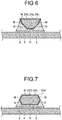
- FIG. 6 is a cross-sectional view of a lead portion of a molded interconnect device according to a second modified example of the second embodiment of the present invention.
- a connecting portion 22C has a hexagonal shape in a cross-section perpendicular to an extending direction thereof.
- an angle formed between a surface f4 and each of extending surfaces of surfaces f2 and f3 and an angle formed between the surface f4 and each of surfaces f5 and f6 is 80 degrees or less in order to obtain an effect of laser beam irradiation.
- a leg portion not illustrated does not need to have a cross-sectional shape same as that of the connecting portion 22C as far as provided is the shape in which an entire outer periphery can be irradiated with laser beams in two opposing directions.
- the connecting portion 22C since a length of the surface f1 is shorter than the opposing surface f4, a length of the external electrode 4 to be connected can be shortened, and packaging density of the external substrate 3 can be improved. Additionally, manufacturing processes can be shortened because the connecting portion 22C has the shape in which the entire outer periphery can be irradiated with laser beams from the two opposing directions, in other words, the surface f4 can be irradiated in the case where the laser beams is emitted from above, and the surfaces f1 to f3, f5, and f6 can be irradiated in the case of emitting the laser beams from below.
- FIG. 7 is a cross-sectional view of a lead portion of a molded interconnect device according to a third modified example of the second embodiment of the present invention.
- a connecting portion 22D has a hexagonal shape in a cross-section perpendicular to an extending direction thereof.
- an angle formed between a surface f4 and each of extending surfaces of surfaces f2 and f3 and an angle formed between a surface f1 and each of extending surfaces of surfaces f5 and f6 is 80 degrees or less in order to obtain an effect of laser beam irradiation.
- a leg portion not illustrated does not need to have a cross-sectional shape same as that of the connecting portion 22D as far as provided is the shape in which an entire outer periphery can be irradiated with laser beams in two opposing directions.
- connection strength can be further improved when connected to the external electrode 4 by solder 5. Additionally, manufacturing processes can be shortened because the connecting portion 22D has the shape in which the entire outer periphery can be irradiated when laser beams are emitted from the two opposing directions, in other words, the surfaces f4 to f6 can be irradiated in the case of emitting the laser beams from above, and the surfaces f1 to f3 can be irradiated in the case of emitting the laser beams from below.
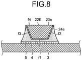
- FIG. 8 is a cross-sectional view of a lead portion of a molded interconnect device according to a fourth modified example of the second embodiment of the present invention.
- a connecting portion 22E has a trapezoidal shape in which a length of a bottom surface f1 is shorter than a top surface f4 in a cross-section perpendicular to an extending direction thereof.
- a metal film 24e is formed on the surface f1 that is the bottom surface and surfaces f2 and f3 adjacent to the surface f1, and is not formed on the surface f4 that is the top surface.
- an angle between the surface f4 and each of the surfaces f2 and f3 is 80 degrees or less in order to obtain an effect of laser beam irradiation.
- the metal film 24e is formed on the surface f1 that is the bottom surface and the surfaces f2 and f3 adjacent to the surface f1, solder fillets are formed on the surfaces f2 and f3, and the connecting portion 22E can ensure connection strength. Additionally, manufacturing processes can be further shortened because the metal film 24e can be formed by irradiating the surfaces f1 to f3 with laser beams from a lower side. Meanwhile, a leg portion not illustrated has a surface that can be irradiated from the lower side, and the metal film is formed on the surface irradiated with the laser beams, and the metal film 24e of the connecting portion 22E is electrically connected to a circuit portion of the main body.
Landscapes
- Wire Bonding (AREA)
- Structures Or Materials For Encapsulating Or Coating Semiconductor Devices Or Solid State Devices (AREA)
- Lead Frames For Integrated Circuits (AREA)
- Physics & Mathematics (AREA)
- Geometry (AREA)
- Injection Moulding Of Plastics Or The Like (AREA)
- Manufacturing Of Printed Wiring (AREA)
- Structure Of Printed Boards (AREA)
Abstract
Description
- The present invention relates to a molded interconnect device, a manufacturing method for a molded interconnect device, and a circuit module.
- In the related art, a semiconductor package having a lead frame connected to an external substrate, and formed by sealing a semiconductor chip with a mold resin is widely used (refer to
Patent Literature 1, for example). Such a semiconductor package is demanded to be downsized, but it is technically difficult to keep product precision while reducing the size of the semiconductor package in which the lead frame is molded by insert molding. - In recent years, developed is a molded interconnect device (hereinafter referred to as "MID") in which a three-dimensional circuit is formed in a main body of a three-dimensional structure in order to downsize the device and reduce the number of components and assembly man-hours (refer to
Patent Literature 2 to 5, for example). -
- Patent Literature 1:
JP 2014-216554 A - Patent Literature 2:
JP 2965803 B - Patent Literature 3:
JP 11-145583 A - Patent Literature 4:
JP 2002-314217 A - Patent Literature 5:
JP 2012-149347 A - However, in
Patent Literature 2 to 4, a forming method for a three-dimensional circuit in a main body is disclosed, but nothing is disclosed regarding a molded interconnect device including a lead frame made of a resin material same as the main body and having a metal film on the outer periphery thereof. - The present invention is made in view of the above-described situation and an object of the present invention is to provide a molded interconnect device, a manufacturing method for the molded interconnect device, and a circuit module, including a lead which can be easily manufactured while keeping product precision even when downsized and can be connected to an external substrate. Solution to Problem
- To solve the above-described problem and achieve the object, a molded interconnect device according to the present invention is adapted to form a three-dimensional circuit by using laser beams, and includes: a main body on which the three-dimensional circuit is formed; and a lead portion connected to an external electrode of an external substrate by solder and extending from the main body, the lead portion including: a lead main body molded from a material same as a material of the main body; and a metal film formed on at least a part of an outer periphery of the lead main body.
- Moreover, in the above-described molded interconnect device according to the present invention, the lead portion includes: a leg portion extending outward from the main body; and a connecting portion connected to the external electrode of the external substrate, the connecting portion at least includes a bottom surface parallel to the external electrode in a cross-section perpendicular to an extending direction of the connecting portion, and also has a shape whose entire outer periphery is capable of being irradiated with laser beams from two opposing directions, and the leg portion has a shape whose entire outer periphery is capable of being irradiated with laser beams from two opposing directions.
- Moreover, in the above-described molded interconnect device according to the present invention, the lead portion includes: a leg portion extending outward from the main body; and a connecting portion connected to the external electrode of the external substrate, the connecting portion includes at least a bottom surface parallel to the external electrode in a cross-section perpendicular to an extending direction of the connecting portion, and also has a shape in which the bottom surface and a side surface adjacent to the bottom surface are irradiated with laser beams at the time of irradiating the connecting portion with laser beams from the bottom surface direction.
- Moreover, a manufacturing method for any one of the above-described molded interconnect device according to the present invention includes: molding a main body and a lead main body; irradiating the main body and the lead main body with laser beams; and forming, by electroless plating, a circuit portion and a metal film respectively on the main body and the lead main body irradiated with laser beams.
- Moreover, a circuit module according to the present invention includes: any one of the above-described molded interconnect device; and an external substrate including an external electrode to which a lead portion of the molded interconnect device is solder-connected. Advantageous Effects of Invention
- According to the present invention, the main body and the lead main body of the molded interconnect device can be simultaneously molded in the molding process, and the three-dimensional circuit and the metal film of the lead main body can be simultaneously formed in the plating process. Therefore, the molded interconnect device including a lead portion can be manufactured by the small number of processes while keeping product precision even when downsized.
-
-
FIG. 1A is a top view of a circuit module using a molded interconnect device according to a first embodiment of the present invention. -
FIG. 1B is a side view of the circuit module inFIG. 1A . -
FIG. 1C is a cross-sectional view taken along a line A-A inFIG. 1B . -
FIG. 2 is a flowchart describing manufacturing processes of the circuit module inFIGS. 1A to 1C . -
FIG. 3A is a top view of a circuit module using a molded interconnect device according to a second embodiment of the present invention. -
FIG. 3B is a side view of the circuit module inFIG. 3A . -
FIG. 3C is a cross-sectional view taken along a line B-B inFIG. 3B . -
FIG. 4 is a view to describe irradiation of laser beams on a lead main body of the molded interconnect device according to the second embodiment. -
FIG. 5 is a cross-sectional view of a lead portion of a molded interconnect device according to a first modified example of the second embodiment of the present invention. -
FIG. 6 is a cross-sectional view of a lead portion of a molded interconnect device according to a second modified example of the second embodiment of the present invention. -
FIG. 7 is a cross-sectional view of a lead portion of a molded interconnect device according to a third modified example of the second embodiment of the present invention. -
FIG. 8 is a cross-sectional view of a lead portion of a molded interconnect device according to a fourth modified example of the second embodiment of the present invention. Description of Embodiments - In the following description, a molded interconnect device and a circuit module using the molded interconnect device will be described as a mode to implement the present invention (hereinafter referred to as "embodiment"). Additionally, note that the present invention is not limited by the embodiment. Furthermore, in the drawings, a same portion is denoted by a same reference sign. Moreover, it should be noted that the drawings are schematically illustrated and a relation between a thickness and a width of each member, a proportion of each member, and the like may differ from those used in practice. Also, note that the drawings may include a portion having sizes or proportions different from each other.
-
FIG. 1A is a top view of a circuit module using a molded interconnect device according to first embodiment of the present invention.FIG. 1B is a side view of the circuit module inFIG. 1A. FIG. 1C is a cross-sectional view taken along a line A-A inFIG. 1B . A moldedinterconnect device 10 according to the first embodiment includes amain body 1 having a three-dimensional circuit formed thereon and alead portion 2 connected to an external electrode of an external substrate by solder and extending from themain body 1. Themain body 1 is made of a resin material that can be subjected to injection molding. Additionally, acircuit module 20 includes the moldedinterconnect device 10 and anexternal substrate 3, and theexternal substrate 3 includes anexternal electrode 4 to which thelead portion 2 of the moldedinterconnect device 10 is connected bysolder 5. InFIGS. 1A to 1C , illustration of a three-dimensional circuit is omitted for simplicity. - The
lead portion 2 has aleg portion 21 extending outward from themain body 1 and a connectingportion 22 connected to the external electrode of the external substrate, and is bent between theleg portion 21 and the connectingportion 22. - As illustrated in
FIG. 1C , thelead portion 2 includes a leadmain body 23 molded from a material same as that of themain body 1, namely, the resin material that can be subjected to injection molding, and ametal film 24 adapted to cover an entire outer periphery of the leadmain body 23. The leadmain body 23 is formed simultaneously with themain body 1 by injection molding. - Next, a manufacturing method for the
circuit module 20 will be described.FIG. 2 is a flowchart describing manufacturing processes of thecircuit module 20 inFIGS. 1A to 1C . - The processes in
FIG. 2 corresponds to manufacturing the moldedinterconnect device 10 by laser direct structuring (LDS). First, themain body 1 and the leadmain body 23 are formed by injection molding or the like (step S1). The resin material that is the material of themain body 1 and the leadmain body 23 is added with an organometallic complex. - After the molding process (step S1), the
main body 1 and the leadmain body 23 are irradiated with laser beams (step S2). A circuit forming portion of themain body 1 and a metal film forming portion of the leadmain body 23 are irradiated with laser beams. Surfaces of themain body 1 and the leadmain body 23 are slightly removed by irradiation with the laser beams, and also the organometallic complex combined in the resin material is activated, and plating can be performed. - After the laser irradiation process (step S2), a circuit portion and the
metal film 24 are formed on themain body 1 and the leadmain body 23 by electroless plating (step S3). The electroless plating is carried out by immersion with plating solution for a desired circuit portion and themetal film 24, for example, immersion with electroless copper plating solution in the case of forming a copper film. Themetal film 24 may be obtained by forming a film by electroless plating and then further forming a film by electroplating, and also may be obtained by stacking films of different metal kinds. - After the plating processes (step S3), the molded
interconnect device 10 is positioned such that the connectingportion 22 is positioned on theexternal electrode 4 applied with solder, and then the connectingportion 22 is connected to theexternal electrode 4 by heating and melting the solder (step S4). - In the above processes, as for the resin material that is the material of the
main body 1 and the leadmain body 23, syndiotactic polystyrene, liquid crystal polymer, or the like, which can be plated by laser irradiation, may also be used instead of the resin material containing the organometallic complex. - Additionally, the molded
interconnect device 10 can also be manufactured by a known microscopic integrated processing technology (MIPTEC) or SKW-L1 instead of the above-described LDS. - For example, in the MIPTEC, the
main body 1 and the leadmain body 23 are processed by molding such as injection molding, and then a thin metal film is formed on themain body 1 and the entire portion of the leadmain body 23 by chemical plating, sputtering, or the like. After that, a periphery of the circuit portion is removed by laser beams and then subjected to electroplating, and an excessive thin metal film is etched. The moldedinterconnect device 10 can be manufactured by forming themetal film 24 by electroplating without laser beam irradiation on the thin metal film formed on the leadmain body 23. - Additionally, in the SKW-L1, the
main body 1 and the leadmain body 23 are processed by molding such as injection molding, the moldedmain body 1 and entire surfaces of the leadmain body 23 are roughened by etching or the like, and a catalyst is applied to the entire portions. After that, the thin metal film is formed on themain body 1 and the entire leadmain body 23 by electroless plating, the periphery of the circuit portion is removed by laser beams, and electroplating is performed, and then an excessive thin metal film is etched. The moldedinterconnect device 10 can be manufactured by forming themetal film 24 by electroplating without laser beam irradiation on the thin metal film formed on the leadmain body 23. - In the first embodiment, since the
lead portion 2 is formed by injection molding and plating without performing insert molding for a metal-made lead, the moldedinterconnect device 10 having excellent precision can be achieved even when downsized. - In a molded interconnect device according to a second embodiment, a connecting portion has a trapezoidal cross-sectional shape.
FIG. 3A is a top view of a circuit module using the molded interconnect devices according to the second embodiment of the present invention.FIG. 3B is a side view of the circuit module inFIG. 3A. 3C is a cross-sectional view taken along a line B-B inFIG. 3B . Note that illustration of a three-dimensional circuit is omitted inFIGS. 3A to 3C in a manner similar to a first embodiment. - As illustrated in
FIG. 3C , similar to a moldedinterconnect device 10 of the first embodiment, a moldedinterconnect device 10A according to the second embodiment includes alead portion 2A including: a leadmain body 23a molded from a material same as amain body 1A, namely, a resin material that can be subjected to injection molding; and ametal film 24a adapted to cover an entire outer periphery of the leadmain body 23a. Thelead portion 2A is formed of aleg portion 21A extending outward from themain body 1A and a connectingportion 22A connected to anexternal electrode 4 of anexternal substrate 3, and is bent between theleg portion 21A and the connectingportion 22A. The connectingportion 22A has a trapezoidal shape in which a length of a bottom surface f1 in the cross-section perpendicular to the extending direction is shorter than that of a surface f4 that is a top surface. Additionally, themain body 1A also has a quadrangular frustum shape obtained by cutting an upper portion of a square pyramid. - The connecting
portion 22A has a shape in which the entire outer periphery can be irradiated with laser beams from two opposing directions. Furthermore, the connectingportion 22A has the surface f1 parallel to theexternal electrode 4 in the cross-section perpendicular to the extending direction of the connectingportion 22A. Since the surface f1 parallel to theexternal electrode 4 is provided, connection strength can be improved when connected to theexternal electrode 4 bysolder 5. Additionally, since the length of the surface f1 is shorter than the opposing surface f4, a length of theexternal electrode 4 to be connected can be shortened, and packaging density of theexternal substrate 3 can be improved. - As far as provided is the shape in which the entire outer periphery can be irradiated with laser beams at the time of emitting the laser beams from two directions opposing to the
leg portion 21A (same direction as an emitting direction of the laser beams to the connectingportion 22A), theleg portion 21A does not need have the cross-sectional shape same as that of the connectingportion 22A. - Furthermore, the molded
interconnect device 10A according to the second embodiment is manufactured by LDS, but has a shape such that the entire outer periphery of the connectingportion 22A can be irradiated with laser beams from the two directions opposing to the connectingportion 22A. - A method of irradiating the connecting
portion 22A (leadmain body 23a before forming themetal film 24a inFIG. 4 ) with laser beams will be described with reference toFIG. 4 . - To irradiate the lead
main body 23a with laser beams, the surface f4 that is the upper surface of the leadmain body 23a is first irradiated with the laser beams by alaser irradiation device 30, and also the surface f4 of the leadmain body 23a is slightly removed and a resin material is activated. After that, the entire outer periphery of the leadmain body 23a can be irradiated with laser beams by rotating the surface f1 of the leadmain body 23a so as to become an upper surface, and irradiating surfaces f1, f2, and f3 of the leadmain body 23a with the laser beams. In the case where an angle formed between the surface f2 or f3 and the laser beams is less than 10 degrees, an effect of laser beam irradiation may not be obtained. Therefore, preferably, the angle formed between the surfaces f2 or f3 and the laser beam is 10 degrees or more, in other words, preferably, the angle between the surface f4 and each of the surfaces f2 and f3 is 80 degrees or less. - Additionally, in
FIG. 4 , onelaser irradiation device 30 may be installed for each of the surface f4 and the surface f1 of the leadmain body 23a in a vertical direction, and the surfaces f1 to f4 of the leadmain body 23a may also be irradiated with laser beams simultaneously from the vertical two directions. In the present specification, "emitting laser beams from two opposing directions" includes: a case of "emitting laser beams simultaneously from a laser irradiation device installed in each of opposing directions"; and a case of "emitting laser beams to any surface of the connecting portion from one laser irradiation device, and rotating the connecting portion by 180 degrees, and then emitting the laser beams to a surface side opposing the surface first irradiated with the laser beams". - On the other hand, for example, in the molded
interconnect device 10 of the first embodiment having a cross-section perpendicular to an extending direction of a connectingportion 22, the number of processes is increased in the case of irradiating surfaces f1, f2, f3, and f4 with laser beams because it is necessary to reset the moldedinterconnect device 10 even in the case where twolaser irradiation devices 30 are provided in opposing directions, and further it is also necessary to reset the moldedinterconnect device 10 three times such that the surfaces f1 to f4 are irradiated respectively in the case of having one laser irradiation device. Meanwhile, in terms of facilitating positioning of the moldedinterconnect device 10A at the time of laser beam irradiation, laser beams are emitted from two opposing directions of either "vertical" or "horizontal" direction. - Since the connecting
portion 22A of the moldedinterconnect device 10A according to the second embodiment has the trapezoidal shape, the number of laser irradiation processes can be reduced and a manufacturing processes can be shortened. Moreover, even when the moldedinterconnect device 10A is downsized, the lead portion can be easily manufactured with high precision. Furthermore, the shape ofmain body 1A of the moldedinterconnect device 10A is a shape, namely, the quadrangular frustum shape in which the entire outer periphery can be irradiated with laser beams from the two opposing directions (the same direction as the laser beam emitting direction to the connectingportion 22A), a time required for the laser irradiation process can be reduced. - Meanwhile, in the second embodiment, as far as provided is the shape in which the entire outer periphery can be irradiated with laser beams from the two opposing directions (direction same as the laser beam emitting direction to the connecting
portion 22A), the shape of themain body 1A is not limited to the quadrangular frustum shape. - Additionally, as far as provided is the shape in which the entire outer periphery can be irradiated with laser beams from the two opposing directions, the shape of the cross-section perpendicular to the extending direction of the connecting portion is not limited to the shape of the second embodiment.
FIG. 5 is a cross-sectional view of a lead portion of a molded interconnect device according to a first modified example of the second embodiment of the present invention. - In the molded interconnect device according to the first modified example of the second embodiment, a connecting
portion 22B has a trapezoidal shape in which a length of a surface f1 that is a bottom surface in a cross-section perpendicular to an extending direction is longer than that of a surface f4 that is a top surface. Additionally, preferably, an angle between the surface f1 and each of surfaces f2 and f3 is 80 degrees or less in order to obtain an effect of laser beam irradiation. A leg portion not illustrated does not need to have a cross-sectional shape same as that of the connectingportion 22B as far as provided is the shape in which an entire outer periphery can be irradiated with laser beams from two opposing directions. - Since the connecting
portion 22B has the surface f1 parallel to anexternal electrode 4 in the cross-section perpendicular to the extending direction of the connectingportion 22B and furthermore the surface f1 has the long length, connection strength can be further improved when connected to theexternal electrode 4 bysolder 5. Additionally, manufacturing processes can be shortened because the connectingportion 22B has the shape in which the entire outer periphery can be irradiated with laser beams from the two opposing directions, in other words, the surfaces f2, f3, and f4 can be irradiated in the case of emitting the laser beams from above and the surface f1 can be irradiated in the case of emitting the laser beams from below. - Additionally, as far as provided is the shape in which the entire outer periphery can be irradiated with laser beams from the two opposing directions, the shape of the cross-section perpendicular to the extending direction of the connecting portion is not limited to the trapezoidal shape.
FIG. 6 is a cross-sectional view of a lead portion of a molded interconnect device according to a second modified example of the second embodiment of the present invention. - In the molded interconnect device according to the second modified example of the second embodiment, a connecting
portion 22C has a hexagonal shape in a cross-section perpendicular to an extending direction thereof. Preferably, an angle formed between a surface f4 and each of extending surfaces of surfaces f2 and f3 and an angle formed between the surface f4 and each of surfaces f5 and f6 is 80 degrees or less in order to obtain an effect of laser beam irradiation. A leg portion not illustrated does not need to have a cross-sectional shape same as that of the connectingportion 22C as far as provided is the shape in which an entire outer periphery can be irradiated with laser beams in two opposing directions. - In the connecting
portion 22C, since a length of the surface f1 is shorter than the opposing surface f4, a length of theexternal electrode 4 to be connected can be shortened, and packaging density of theexternal substrate 3 can be improved. Additionally, manufacturing processes can be shortened because the connectingportion 22C has the shape in which the entire outer periphery can be irradiated with laser beams from the two opposing directions, in other words, the surface f4 can be irradiated in the case where the laser beams is emitted from above, and the surfaces f1 to f3, f5, and f6 can be irradiated in the case of emitting the laser beams from below. - Additionally, as far as the provided is the shape in which the entire outer periphery can be irradiated with laser beams from the two opposing directions, the shape of the cross-section perpendicular to the extending direction of the connecting portion may have a shape illustrated in
FIG. 7. FIG. 7 is a cross-sectional view of a lead portion of a molded interconnect device according to a third modified example of the second embodiment of the present invention. - In the molded interconnect device according to the third modified example of the second embodiment, a connecting
portion 22D has a hexagonal shape in a cross-section perpendicular to an extending direction thereof. Preferably, an angle formed between a surface f4 and each of extending surfaces of surfaces f2 and f3 and an angle formed between a surface f1 and each of extending surfaces of surfaces f5 and f6 is 80 degrees or less in order to obtain an effect of laser beam irradiation. A leg portion not illustrated does not need to have a cross-sectional shape same as that of the connectingportion 22D as far as provided is the shape in which an entire outer periphery can be irradiated with laser beams in two opposing directions. - Since the connecting
portion 22D has the surface f1 parallel to anexternal electrode 4 and a length of the surface f1 is long, connection strength can be further improved when connected to theexternal electrode 4 bysolder 5. Additionally, manufacturing processes can be shortened because the connectingportion 22D has the shape in which the entire outer periphery can be irradiated when laser beams are emitted from the two opposing directions, in other words, the surfaces f4 to f6 can be irradiated in the case of emitting the laser beams from above, and the surfaces f1 to f3 can be irradiated in the case of emitting the laser beams from below. - Additionally, a metal film may not be needed to be formed on an entire outer periphery of a lead main body.
FIG. 8 is a cross-sectional view of a lead portion of a molded interconnect device according to a fourth modified example of the second embodiment of the present invention. In the molded interconnect device according to the fourth modified example of second embodiment, a connectingportion 22E has a trapezoidal shape in which a length of a bottom surface f1 is shorter than a top surface f4 in a cross-section perpendicular to an extending direction thereof. Furthermore, ametal film 24e is formed on the surface f1 that is the bottom surface and surfaces f2 and f3 adjacent to the surface f1, and is not formed on the surface f4 that is the top surface. Additionally, preferably, an angle between the surface f4 and each of the surfaces f2 and f3 is 80 degrees or less in order to obtain an effect of laser beam irradiation. - Since the
metal film 24e is formed on the surface f1 that is the bottom surface and the surfaces f2 and f3 adjacent to the surface f1, solder fillets are formed on the surfaces f2 and f3, and the connectingportion 22E can ensure connection strength. Additionally, manufacturing processes can be further shortened because themetal film 24e can be formed by irradiating the surfaces f1 to f3 with laser beams from a lower side. Meanwhile, a leg portion not illustrated has a surface that can be irradiated from the lower side, and the metal film is formed on the surface irradiated with the laser beams, and themetal film 24e of the connectingportion 22E is electrically connected to a circuit portion of the main body. -
- 1, 1A Main body
- 2, 2A Lead portion
- 3 External substrate
- 4 External electrode
- 5 Solder
- 10, 10A Molded interconnect device
- 20, 20A Circuit module
- 21, 21A Leg
- 22, 22A, 22B, 22C, 22D, 22E Connecting portion
- 23, 23a, 23b, 23c, 23e Lead main body
- 24, 24a, 24b, 24c, 24e Metal film
- 30 Laser irradiation device
Claims (5)
- A molded interconnect device adapted to form a three-dimensional circuit by using laser beams, comprising:a main body on which the three-dimensional circuit is formed; anda lead portion connected to an external electrode of an external substrate by solder and extending from the main body, the lead portion including:a lead main body molded from a material same as a material of the main body; anda metal film formed on at least a part of an outer periphery of the lead main body.
- The molded interconnect device according to claim 1, wherein
the lead portion includes:a leg portion extending outward from the main body; anda connecting portion connected to the external electrode of the external substrate,the connecting portion at least includes a bottom surface parallel to the external electrode in a cross-section perpendicular to an extending direction of the connecting portion, and also has a shape whose entire outer periphery is capable of being irradiated with laser beams from two opposing directions, and
the leg portion has a shape whose entire outer periphery is capable of being irradiated with laser beams from two opposing directions. - The molded interconnect device according to claim 1, wherein
the lead portion includes:a leg portion extending outward from the main body; anda connecting portion connected to the external electrode of the external substrate,the connecting portion includes at least a bottom surface parallel to the external electrode in a cross-section perpendicular to an extending direction of the connecting portion, and also has a shape in which the bottom surface and a side surface adjacent to the bottom surface are irradiated with laser beams at the time of irradiating the connecting portion with laser beams from the bottom surface direction. - A manufacturing method for the molded interconnect device according to any one of claims 1 to 3, comprising:molding a main body and a lead main body;irradiating the main body and the lead main body with laser beams; andforming, by electroless plating, a circuit portion and a metal film respectively on the main body and the lead main body irradiated with laser beams.
- A circuit module comprising:the molded interconnect device according to any one of claims 1 to 3; andan external substrate including an external electrode to which a lead portion of the molded interconnect device is solder-connected.
Applications Claiming Priority (2)
| Application Number | Priority Date | Filing Date | Title |
|---|---|---|---|
| JP2015072734A JP6338547B2 (en) | 2015-03-31 | 2015-03-31 | Molded circuit component, method for manufacturing molded circuit component, and circuit module |
| PCT/JP2016/055698 WO2016158117A1 (en) | 2015-03-31 | 2016-02-25 | Molded circuit component, method for manufacturing molded circuit component, and circuit module |
Publications (2)
| Publication Number | Publication Date |
|---|---|
| EP3279937A1 true EP3279937A1 (en) | 2018-02-07 |
| EP3279937A4 EP3279937A4 (en) | 2018-12-05 |
Family
ID=57007032
Family Applications (1)
| Application Number | Title | Priority Date | Filing Date |
|---|---|---|---|
| EP16772001.0A Withdrawn EP3279937A4 (en) | 2015-03-31 | 2016-02-25 | Molded circuit component, method for manufacturing molded circuit component, and circuit module |
Country Status (5)
| Country | Link |
|---|---|
| US (1) | US10304762B2 (en) |
| EP (1) | EP3279937A4 (en) |
| JP (1) | JP6338547B2 (en) |
| CN (1) | CN107251219B (en) |
| WO (1) | WO2016158117A1 (en) |
Families Citing this family (2)
| Publication number | Priority date | Publication date | Assignee | Title |
|---|---|---|---|---|
| US11545418B2 (en) * | 2018-10-24 | 2023-01-03 | Texas Instruments Incorporated | Thermal capacity control for relative temperature-based thermal shutdown |
| CN114008773A (en) | 2019-06-14 | 2022-02-01 | 罗姆股份有限公司 | Semiconductor device and method for manufacturing semiconductor device |
Family Cites Families (23)
| Publication number | Priority date | Publication date | Assignee | Title |
|---|---|---|---|---|
| JP2965803B2 (en) | 1992-11-19 | 1999-10-18 | ポリプラスチックス株式会社 | Method for forming conductive circuit on surface of molded article and conductive circuit forming part |
| JP3230348B2 (en) * | 1993-09-06 | 2001-11-19 | ソニー株式会社 | Resin-sealed semiconductor device and method of manufacturing the same |
| JP2644194B2 (en) * | 1994-08-31 | 1997-08-25 | 秋田日本電気株式会社 | Semiconductor device and manufacturing method thereof |
| JPH10294395A (en) * | 1997-04-18 | 1998-11-04 | Hitachi Cable Ltd | Semiconductor element mounting substrate and semiconductor device |
| US5879965A (en) | 1997-06-19 | 1999-03-09 | Micron Technology, Inc. | Plastic lead frames for semiconductor devices, packages including same, and methods of fabrication |
| JP3616488B2 (en) | 1997-11-10 | 2005-02-02 | 三共化成株式会社 | Manufacturing method of molded circuit components |
| US6924548B2 (en) | 2001-01-31 | 2005-08-02 | Hitachi, Ltd. | Semiconductor device and its manufacturing method with leads that have an inverted trapezoid-like section |
| JP2002314217A (en) | 2001-04-12 | 2002-10-25 | Hitachi Cable Ltd | Manufacturing method of plastic molded circuit parts |
| US7315077B2 (en) * | 2003-11-13 | 2008-01-01 | Fairchild Korea Semiconductor, Ltd. | Molded leadless package having a partially exposed lead frame pad |
| US7134197B2 (en) * | 2003-12-18 | 2006-11-14 | Honeywell International Inc. | Plastic lead frames utilizing reel-to-reel processing |
| US7112873B2 (en) * | 2004-09-03 | 2006-09-26 | Honeywell International Inc. | Flip chip metal bonding to plastic leadframe |
| US8492464B2 (en) * | 2008-05-23 | 2013-07-23 | Sabic Innovative Plastics Ip B.V. | Flame retardant laser direct structuring materials |
| TW201036504A (en) * | 2009-03-18 | 2010-10-01 | Everlight Electronics Co Ltd | Photoelectric transmitting or receiving device and manufacturing method thereof |
| US20100307799A1 (en) * | 2009-06-06 | 2010-12-09 | Chiang Cheng-Feng | Carrier Structure for Electronic Components and Fabrication Method of the same |
| JP5455028B2 (en) * | 2009-10-30 | 2014-03-26 | パナソニック株式会社 | Circuit board structure |
| EP2354185A1 (en) * | 2010-02-08 | 2011-08-10 | Mitsubishi Chemical Europe GmbH | Polymer composition |
| CN102237568B (en) * | 2010-04-30 | 2015-09-23 | 上海莫仕连接器有限公司 | Antenna assembly and preparation method thereof |
| JP5437943B2 (en) * | 2010-07-26 | 2014-03-12 | 日立オートモティブシステムズ株式会社 | Power semiconductor unit, power module and manufacturing method thereof |
| DE102011000138A1 (en) | 2011-01-14 | 2012-07-19 | Lpkf Laser & Electronics Ag | Method for the selective metallization of a substrate and a circuit carrier produced by this method |
| TW201303055A (en) * | 2011-07-07 | 2013-01-16 | Hon Hai Prec Ind Co Ltd | Crucible, vacuum evaporation system and method using the same |
| US8708745B2 (en) * | 2011-11-07 | 2014-04-29 | Apple Inc. | Dual orientation electronic connector |
| JP6270335B2 (en) | 2013-04-26 | 2018-01-31 | オリンパス株式会社 | Imaging device |
| DE102014206558B4 (en) * | 2014-04-04 | 2025-11-20 | Robert Bosch Gmbh | Method for manufacturing a MID circuit carrier and MID circuit carrier |
-
2015
- 2015-03-31 JP JP2015072734A patent/JP6338547B2/en not_active Expired - Fee Related
-
2016
- 2016-02-25 EP EP16772001.0A patent/EP3279937A4/en not_active Withdrawn
- 2016-02-25 CN CN201680012094.1A patent/CN107251219B/en not_active Expired - Fee Related
- 2016-02-25 WO PCT/JP2016/055698 patent/WO2016158117A1/en not_active Ceased
-
2017
- 2017-08-28 US US15/688,631 patent/US10304762B2/en active Active
Also Published As
| Publication number | Publication date |
|---|---|
| JP2016192521A (en) | 2016-11-10 |
| EP3279937A4 (en) | 2018-12-05 |
| CN107251219B (en) | 2019-09-10 |
| WO2016158117A1 (en) | 2016-10-06 |
| JP6338547B2 (en) | 2018-06-06 |
| CN107251219A (en) | 2017-10-13 |
| US10304762B2 (en) | 2019-05-28 |
| US20170358526A1 (en) | 2017-12-14 |
Similar Documents
| Publication | Publication Date | Title |
|---|---|---|
| US10431560B2 (en) | Molded semiconductor package having an optical inspection feature | |
| CN111434191B (en) | Method and apparatus for integrating semiconductor wafers | |
| JP2016119366A5 (en) | ||
| JP7782011B2 (en) | Substrate for semiconductor device and semiconductor device | |
| US9848496B2 (en) | Electronic component module and manufacturing method thereof | |
| US20130115738A1 (en) | Packaging substrate and fabrication method thereof | |
| EP3279937A1 (en) | Molded circuit component, method for manufacturing molded circuit component, and circuit module | |
| JP2011187742A (en) | Substrate for mounting semiconductor element, and method of manufacturing the same | |
| JP2017036500A5 (en) | ||
| US10147615B2 (en) | Fabrication method of package structure | |
| US20180139840A1 (en) | Fabrication method of substrate structure | |
| CN105405819A (en) | Metallized wafer level packaging method | |
| CN210182335U (en) | Five-sided metal encapsulated package structure | |
| TW201511149A (en) | Integrated circuit package system with plated leads and manufacturing method thereof | |
| US9252089B2 (en) | Universal lead frame for flat no-leads packages | |
| CN102779722A (en) | Method for unsealing integrated circuit package | |
| KR102102034B1 (en) | Manufacturing method of qfn semiconductor package | |
| US20150156865A1 (en) | Coreless board for semiconductor package, method of manufacturing the same, and method of manufacturing semiconductor package using the same | |
| JP6345957B2 (en) | Metal-ceramic circuit board and manufacturing method thereof | |
| TWI716476B (en) | Electrical-contact assemblies | |
| WO2016017094A1 (en) | Electronic circuit component | |
| TWI625799B (en) | Manufacturing method of lead frame structure | |
| JP5913486B2 (en) | Plating rack | |
| JP5098452B2 (en) | Manufacturing method of semiconductor device | |
| US9013048B2 (en) | Semiconductor device manufacturing method and semiconductor device |
Legal Events
| Date | Code | Title | Description |
|---|---|---|---|
| STAA | Information on the status of an ep patent application or granted ep patent |
Free format text: STATUS: THE INTERNATIONAL PUBLICATION HAS BEEN MADE |
|
| PUAI | Public reference made under article 153(3) epc to a published international application that has entered the european phase |
Free format text: ORIGINAL CODE: 0009012 |
|
| STAA | Information on the status of an ep patent application or granted ep patent |
Free format text: STATUS: REQUEST FOR EXAMINATION WAS MADE |
|
| 17P | Request for examination filed |
Effective date: 20171004 |
|
| AK | Designated contracting states |
Kind code of ref document: A1 Designated state(s): AL AT BE BG CH CY CZ DE DK EE ES FI FR GB GR HR HU IE IS IT LI LT LU LV MC MK MT NL NO PL PT RO RS SE SI SK SM TR |
|
| AX | Request for extension of the european patent |
Extension state: BA ME |
|
| DAV | Request for validation of the european patent (deleted) | ||
| DAX | Request for extension of the european patent (deleted) | ||
| A4 | Supplementary search report drawn up and despatched |
Effective date: 20181029 |
|
| RIC1 | Information provided on ipc code assigned before grant |
Ipc: H01L 23/498 20060101ALI20181020BHEP Ipc: H01L 21/48 20060101ALI20181020BHEP Ipc: H01L 23/31 20060101AFI20181020BHEP |
|
| STAA | Information on the status of an ep patent application or granted ep patent |
Free format text: STATUS: THE APPLICATION IS DEEMED TO BE WITHDRAWN |
|
| 18D | Application deemed to be withdrawn |
Effective date: 20200901 |