EP3279932A1 - A semiconductor device and manufacture thereof - Google Patents
A semiconductor device and manufacture thereof Download PDFInfo
- Publication number
- EP3279932A1 EP3279932A1 EP17184174.5A EP17184174A EP3279932A1 EP 3279932 A1 EP3279932 A1 EP 3279932A1 EP 17184174 A EP17184174 A EP 17184174A EP 3279932 A1 EP3279932 A1 EP 3279932A1
- Authority
- EP
- European Patent Office
- Prior art keywords
- layer
- dielectric layer
- semiconductor substrate
- contact hole
- opening
- Prior art date
- Legal status (The legal status is an assumption and is not a legal conclusion. Google has not performed a legal analysis and makes no representation as to the accuracy of the status listed.)
- Granted
Links
Images





Classifications
-
- H—ELECTRICITY
- H10—SEMICONDUCTOR DEVICES; ELECTRIC SOLID-STATE DEVICES NOT OTHERWISE PROVIDED FOR
- H10P—GENERIC PROCESSES OR APPARATUS FOR THE MANUFACTURE OR TREATMENT OF DEVICES COVERED BY CLASS H10
- H10P76/00—Manufacture or treatment of masks on semiconductor bodies, e.g. by lithography or photolithography
-
- H—ELECTRICITY
- H10—SEMICONDUCTOR DEVICES; ELECTRIC SOLID-STATE DEVICES NOT OTHERWISE PROVIDED FOR
- H10W—GENERIC PACKAGES, INTERCONNECTIONS, CONNECTORS OR OTHER CONSTRUCTIONAL DETAILS OF DEVICES COVERED BY CLASS H10
- H10W20/00—Interconnections in chips, wafers or substrates
- H10W20/01—Manufacture or treatment
- H10W20/071—Manufacture or treatment of dielectric parts thereof
- H10W20/081—Manufacture or treatment of dielectric parts thereof by forming openings in the dielectric parts
- H10W20/089—Manufacture or treatment of dielectric parts thereof by forming openings in the dielectric parts using processes for implementing desired shapes or dispositions of the openings, e.g. double patterning
-
- H—ELECTRICITY
- H10—SEMICONDUCTOR DEVICES; ELECTRIC SOLID-STATE DEVICES NOT OTHERWISE PROVIDED FOR
- H10D—INORGANIC ELECTRIC SEMICONDUCTOR DEVICES
- H10D62/00—Semiconductor bodies, or regions thereof, of devices having potential barriers
- H10D62/10—Shapes, relative sizes or dispositions of the regions of the semiconductor bodies; Shapes of the semiconductor bodies
-
- H—ELECTRICITY
- H10—SEMICONDUCTOR DEVICES; ELECTRIC SOLID-STATE DEVICES NOT OTHERWISE PROVIDED FOR
- H10P—GENERIC PROCESSES OR APPARATUS FOR THE MANUFACTURE OR TREATMENT OF DEVICES COVERED BY CLASS H10
- H10P14/00—Formation of materials, e.g. in the shape of layers or pillars
- H10P14/40—Formation of materials, e.g. in the shape of layers or pillars of conductive or resistive materials
-
- H—ELECTRICITY
- H10—SEMICONDUCTOR DEVICES; ELECTRIC SOLID-STATE DEVICES NOT OTHERWISE PROVIDED FOR
- H10W—GENERIC PACKAGES, INTERCONNECTIONS, CONNECTORS OR OTHER CONSTRUCTIONAL DETAILS OF DEVICES COVERED BY CLASS H10
- H10W20/00—Interconnections in chips, wafers or substrates
- H10W20/01—Manufacture or treatment
- H10W20/031—Manufacture or treatment of conductive parts of the interconnections
- H10W20/062—Manufacture or treatment of conductive parts of the interconnections by smoothing of conductive parts, e.g. by planarisation
-
- H—ELECTRICITY
- H10—SEMICONDUCTOR DEVICES; ELECTRIC SOLID-STATE DEVICES NOT OTHERWISE PROVIDED FOR
- H10W—GENERIC PACKAGES, INTERCONNECTIONS, CONNECTORS OR OTHER CONSTRUCTIONAL DETAILS OF DEVICES COVERED BY CLASS H10
- H10W20/00—Interconnections in chips, wafers or substrates
- H10W20/01—Manufacture or treatment
- H10W20/031—Manufacture or treatment of conductive parts of the interconnections
- H10W20/0698—Local interconnections
-
- H—ELECTRICITY
- H10—SEMICONDUCTOR DEVICES; ELECTRIC SOLID-STATE DEVICES NOT OTHERWISE PROVIDED FOR
- H10W—GENERIC PACKAGES, INTERCONNECTIONS, CONNECTORS OR OTHER CONSTRUCTIONAL DETAILS OF DEVICES COVERED BY CLASS H10
- H10W20/00—Interconnections in chips, wafers or substrates
- H10W20/01—Manufacture or treatment
- H10W20/071—Manufacture or treatment of dielectric parts thereof
- H10W20/081—Manufacture or treatment of dielectric parts thereof by forming openings in the dielectric parts
-
- H—ELECTRICITY
- H10—SEMICONDUCTOR DEVICES; ELECTRIC SOLID-STATE DEVICES NOT OTHERWISE PROVIDED FOR
- H10W—GENERIC PACKAGES, INTERCONNECTIONS, CONNECTORS OR OTHER CONSTRUCTIONAL DETAILS OF DEVICES COVERED BY CLASS H10
- H10W20/00—Interconnections in chips, wafers or substrates
- H10W20/01—Manufacture or treatment
- H10W20/071—Manufacture or treatment of dielectric parts thereof
- H10W20/081—Manufacture or treatment of dielectric parts thereof by forming openings in the dielectric parts
- H10W20/082—Manufacture or treatment of dielectric parts thereof by forming openings in the dielectric parts the openings being tapered via holes
-
- H—ELECTRICITY
- H10—SEMICONDUCTOR DEVICES; ELECTRIC SOLID-STATE DEVICES NOT OTHERWISE PROVIDED FOR
- H10W—GENERIC PACKAGES, INTERCONNECTIONS, CONNECTORS OR OTHER CONSTRUCTIONAL DETAILS OF DEVICES COVERED BY CLASS H10
- H10W20/00—Interconnections in chips, wafers or substrates
- H10W20/01—Manufacture or treatment
- H10W20/071—Manufacture or treatment of dielectric parts thereof
- H10W20/081—Manufacture or treatment of dielectric parts thereof by forming openings in the dielectric parts
- H10W20/083—Manufacture or treatment of dielectric parts thereof by forming openings in the dielectric parts the openings being via holes penetrating underlying conductors
-
- H—ELECTRICITY
- H10—SEMICONDUCTOR DEVICES; ELECTRIC SOLID-STATE DEVICES NOT OTHERWISE PROVIDED FOR
- H10W—GENERIC PACKAGES, INTERCONNECTIONS, CONNECTORS OR OTHER CONSTRUCTIONAL DETAILS OF DEVICES COVERED BY CLASS H10
- H10W20/00—Interconnections in chips, wafers or substrates
- H10W20/01—Manufacture or treatment
- H10W20/071—Manufacture or treatment of dielectric parts thereof
- H10W20/093—Manufacture or treatment of dielectric parts thereof by modifying materials of the dielectric parts
- H10W20/096—Manufacture or treatment of dielectric parts thereof by modifying materials of the dielectric parts by contacting with gases, liquids or plasmas
-
- H—ELECTRICITY
- H10—SEMICONDUCTOR DEVICES; ELECTRIC SOLID-STATE DEVICES NOT OTHERWISE PROVIDED FOR
- H10W—GENERIC PACKAGES, INTERCONNECTIONS, CONNECTORS OR OTHER CONSTRUCTIONAL DETAILS OF DEVICES COVERED BY CLASS H10
- H10W20/00—Interconnections in chips, wafers or substrates
- H10W20/20—Interconnections within wafers or substrates, e.g. through-silicon vias [TSV]
-
- H—ELECTRICITY
- H10—SEMICONDUCTOR DEVICES; ELECTRIC SOLID-STATE DEVICES NOT OTHERWISE PROVIDED FOR
- H10W—GENERIC PACKAGES, INTERCONNECTIONS, CONNECTORS OR OTHER CONSTRUCTIONAL DETAILS OF DEVICES COVERED BY CLASS H10
- H10W20/00—Interconnections in chips, wafers or substrates
- H10W20/40—Interconnections external to wafers or substrates, e.g. back-end-of-line [BEOL] metallisations or vias connecting to gate electrodes
- H10W20/41—Interconnections external to wafers or substrates, e.g. back-end-of-line [BEOL] metallisations or vias connecting to gate electrodes characterised by their conductive parts
- H10W20/43—Layouts of interconnections
-
- H—ELECTRICITY
- H10—SEMICONDUCTOR DEVICES; ELECTRIC SOLID-STATE DEVICES NOT OTHERWISE PROVIDED FOR
- H10W—GENERIC PACKAGES, INTERCONNECTIONS, CONNECTORS OR OTHER CONSTRUCTIONAL DETAILS OF DEVICES COVERED BY CLASS H10
- H10W20/00—Interconnections in chips, wafers or substrates
- H10W20/40—Interconnections external to wafers or substrates, e.g. back-end-of-line [BEOL] metallisations or vias connecting to gate electrodes
- H10W20/41—Interconnections external to wafers or substrates, e.g. back-end-of-line [BEOL] metallisations or vias connecting to gate electrodes characterised by their conductive parts
- H10W20/44—Conductive materials thereof
- H10W20/4403—Conductive materials thereof based on metals, e.g. alloys, metal silicides
- H10W20/4437—Conductive materials thereof based on metals, e.g. alloys, metal silicides the principal metal being a transition metal
- H10W20/4441—Conductive materials thereof based on metals, e.g. alloys, metal silicides the principal metal being a transition metal the principal metal being a refractory metal
-
- H—ELECTRICITY
- H10—SEMICONDUCTOR DEVICES; ELECTRIC SOLID-STATE DEVICES NOT OTHERWISE PROVIDED FOR
- H10W—GENERIC PACKAGES, INTERCONNECTIONS, CONNECTORS OR OTHER CONSTRUCTIONAL DETAILS OF DEVICES COVERED BY CLASS H10
- H10W20/00—Interconnections in chips, wafers or substrates
- H10W20/40—Interconnections external to wafers or substrates, e.g. back-end-of-line [BEOL] metallisations or vias connecting to gate electrodes
- H10W20/45—Interconnections external to wafers or substrates, e.g. back-end-of-line [BEOL] metallisations or vias connecting to gate electrodes characterised by their insulating parts
- H10W20/47—Interconnections external to wafers or substrates, e.g. back-end-of-line [BEOL] metallisations or vias connecting to gate electrodes characterised by their insulating parts comprising two or more dielectric layers having different properties, e.g. different dielectric constants
-
- H—ELECTRICITY
- H10—SEMICONDUCTOR DEVICES; ELECTRIC SOLID-STATE DEVICES NOT OTHERWISE PROVIDED FOR
- H10W—GENERIC PACKAGES, INTERCONNECTIONS, CONNECTORS OR OTHER CONSTRUCTIONAL DETAILS OF DEVICES COVERED BY CLASS H10
- H10W20/00—Interconnections in chips, wafers or substrates
- H10W20/01—Manufacture or treatment
- H10W20/031—Manufacture or treatment of conductive parts of the interconnections
- H10W20/056—Manufacture or treatment of conductive parts of the interconnections by filling conductive material into holes, grooves or trenches
-
- H—ELECTRICITY
- H10—SEMICONDUCTOR DEVICES; ELECTRIC SOLID-STATE DEVICES NOT OTHERWISE PROVIDED FOR
- H10W—GENERIC PACKAGES, INTERCONNECTIONS, CONNECTORS OR OTHER CONSTRUCTIONAL DETAILS OF DEVICES COVERED BY CLASS H10
- H10W20/00—Interconnections in chips, wafers or substrates
- H10W20/01—Manufacture or treatment
- H10W20/071—Manufacture or treatment of dielectric parts thereof
- H10W20/074—Manufacture or treatment of dielectric parts thereof of dielectric parts comprising thin functional dielectric layers, e.g. dielectric etch-stop, barrier, capping or liner layers
- H10W20/076—Manufacture or treatment of dielectric parts thereof of dielectric parts comprising thin functional dielectric layers, e.g. dielectric etch-stop, barrier, capping or liner layers in via holes or trenches
- H10W20/0765—Manufacture or treatment of dielectric parts thereof of dielectric parts comprising thin functional dielectric layers, e.g. dielectric etch-stop, barrier, capping or liner layers in via holes or trenches the thin functional dielectric layers being temporary, e.g. sacrificial layers
Definitions
- the present invention relates generally to semiconductor techniques, and more specifically to a semiconductor device and manufacture thereof.
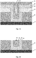
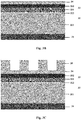
- Figs. 1A and 1B show schematic diagrams of one example of using a conventional semiconductor manufacturing method to form a contact apparatus.
- a dielectric layer 12 is formed on a substrate 11
- an anti-reflective layer 13 is formed on the dielectric layer 12
- the structure on the substrate 11 is patterned to form an opening that goes through the anti-reflective layer 13 and the dielectric layer 12 and exposes a portion of the substrate 11.
- a compound layer is formed on the upper surface of the substrate 11, wherein the compound layer comprises a titanium layer 14 and titanium nitride layer 15.
- a tungsten layer 16 may be deposited on the supper surface of the substrate 11 to form a contact apparatus. Because the side surfaces of the opening are perpendicular to the upper surface of the anti-reflective layer 13, an overhang 17 may be formed on the upper part of the opening during the deposition of the tungsten layer 16, which forms a hollow hole 18 in the tungsten layer 16.
- CMP Chemical Mechanical Polishing
- a first aspect of the present invention provides a method for manufacturing a semiconductor apparatus, comprising: providing a semiconductor substrate; forming a dielectric layer on the semiconductor substrate; forming a functional layer on the dielectric layer, wherein the functional layer is capable of reacting with oxygen; forming a hard mask layer on the functional layer; patterning the semiconductor substrate to form an opening on the semiconductor substrate, wherein the opening goes through the hard mask layer and the functional layer and extends into the dielectric layer; performing an oxidization process on side surfaces of the functional layer inside the opening to form oxide layers; and performing a first process on the semiconductor substrate, wherein the first process comprises: removing a portion of the dielectric layer that is underneath the opening to expose the semiconductor substrate; and removing the oxide layers on the side surfaces of the functional layer to form a contact hole, wherein a first portion of the contact hole is in the functional layer, a second portion of the contact hole is in the dielectric layer, the width of the first portion of the contact hole is larger than the width of the second portion of the contact hole.
- the aforementioned method further entails filling the contact hole with a conductive material to form a contact apparatus.
- the functional layer includes a transitional layer formed on the dielectric layer and an amorphous carbon layer formed on the transitional layer, wherein the transitional layer is an insulated dielectric layer comprising carbon and silicon.
- a carbon concentration in a first side that is adjacent to the amorphous carbon layer is higher than that in a second side that is adjacent to the dielectric layer.
- patterning the semiconductor substrate comprises: forming a patterned photoresist layer on the hard mask layer; and etching the semiconductor substrate with respect to the patterned photoresist layer to form the opening.
- the oxidization process comprises removing the patterned photoresist layer.
- performing an oxidization process on the side surfaces of the functional layer inside the opening may comprise: oxidizing side surfaces of the amorphous carbon layer and the transitional layer inside the opening to remove a portion of the amorphous carbon layer; and forming oxide layers on the side surfaces of the transitional layer.
- the first process may comprise: performing a dry etching process on the semiconductor substrate to remove a portion of the dielectric layer underneath the opening to expose the semiconductor substrate; removing the hard mask layer; and performing a wet etching process on the semiconductor substrate to remove the oxide layers on the side surfaces of the transitional layer to form a contact hole.
- the first process may comprise: removing a portion of the dielectric layer underneath the opening, the hard mask layer and the amorphous carbon layer; and performing a wet etching process on the semiconductor substrate to remove the oxide layers on the side surfaces of the transitional layer to form a contact hole.
- removing a portion of the dielectric layer underneath the opening, the hard mask layer and the amorphous carbon layer may comprise: performing a dry etching process on the semiconductor substrate to remove the hard mask layer and further extend the opening into the dielectric layer; removing the amorphous carbon layer; and performing a dry etching process on the semiconductor substrate to remove a portion of the dielectric layer underneath the opening to expose the semiconductor substrate.
- the oxidization process comprises a processing using oxygen ion.
- the dielectric layer is made of silicon-based oxide.
- the dielectric layer comprises: a first dielectric layer formed on the semiconductor substrate, wherein the first dielectric layer is made of Phosphosilicate Glass (PSG), Borophosphosilicate Glass (BPSG), or silicon-based oxide; and a second dielectric layer formed on the first dielectric layer, wherein the second dielectric layer is made of silicon-based oxide.
- PSG Phosphosilicate Glass
- BPSG Borophosphosilicate Glass
- silicon-based oxide silicon-based oxide
- the aforementioned method further comprises: forming a conductive material layer on the semiconductor substrate, wherein the conductive material layer fills the contact hole; and performing a Chemical Mechanical Polishing (CMP) process on the conductive material layer so that the upper surface of the remaining conductive material layer is on the same horizontal level with the upper surface of the functional layer to form a contact apparatus.
- CMP Chemical Mechanical Polishing
- a second aspect of the present invention provides an alternative semiconductor apparatus, comprising: a semiconductor substrate; a dielectric layer formed on the semiconductor substrate; a functional layer formed on the dielectric layer, wherein the functional layer comprises a transitional layer that is an insulated dielectric layer comprising carbon and silicon; and a contact hole that goes through the functional layer and the dielectric layer and exposes a portion of the semiconductor substrate, wherein a first portion of the contact hole is in the functional layer, a second portion of the contact hole is in the dielectric layer, and the width of the first portion of the contact hole is larger than the width of the second portion of the contact hole.
- the functional layer may further comprise an amorphous carbon layer formed on the transitional layer.
- the functional layer comprises the transitional layer and the amorphous carbon layer formed on the transitional layer.
- a carbon concentration in a first side that is adjacent to the amorphous carbon layer may be higher than that in a second side that is adjacent to the dielectric layer.
- the aforementioned semiconductor apparatus may further comprise a contact apparatus formed by filling the contact hole with a conductive material.
- An apparatus according to the second aspect of the present invention may be obtained by a method according to the first aspect of the present invention.
- Embodiments in the figures may represent idealized illustrations. Variations from the shapes illustrated may be possible, for example due to manufacturing techniques and/or tolerances. Thus, the example embodiments shall not be construed as limited to the shapes or regions illustrated herein but are to include deviations in the shapes. For example, an etched region illustrated as a rectangle may have rounded or curved features. The shapes and regions illustrated in the figures are illustrative and shall not limit the invention.
- first,” “second,” etc. may be used herein to describe various elements, these elements shall not be limited by these terms. These terms may be used to distinguish one element from another element. Thus, a first element discussed below may be termed a second element without departing from the teachings of the present inventive concept. The description of an element as a “first” element may not require or imply the presence of a second element or other elements.
- the terms “first,” “second,” etc. may also be used herein to differentiate different categories or sets of elements. For conciseness, the terms “first,” “second,” etc. may represent “first-category (or first-set),” “second-category (or second-set),” etc., respectively.
- first element such as a layer, film, region, or substrate
- neighbored to or “coupled with” a second element
- the first element can be directly on, directly neighboring, directly connected to or directly coupled with the second element, or an intervening element may also be present between the first element and the second element.
- first element is referred to as being “directly on,” “directly neighboring,” “directly connected to,” or “directly coupled with” a second element, then no intended intervening element (except environmental elements such as air) may also be present between the first element and the second element.
- spatially relative terms such as “beneath,” “below,” “lower,” “above,” “upper,” and the like, may be used herein for ease of description to describe one element or feature's spatial relationship to another element(s) or feature(s) as illustrated in the figures. It will be understood that the spatially relative terms may encompass different orientations of the device in use or operation in addition to the orientation depicted in the figures. For example, if the device in the figures is turned over, elements described as “below” or “beneath” other elements or features would then be oriented “above” the other elements or features. Thus, the term “below” can encompass both an orientation of above and below. The device may be otherwise oriented (rotated 90 degrees or at other orientation), and the spatially relative descriptors used herein shall be interpreted accordingly.
- connection may mean “electrically connect.”
- insulation may mean “electrically insulate.”
- Embodiments of the inventive concept may also cover an article of manufacture that includes a non-transitory computer readable medium on which computer-readable instructions for carrying out embodiments of the inventive technique are stored.
- the computer readable medium may include, for example, semiconductor, magnetic, opto-magnetic, optical, or other forms of computer readable medium for storing computer readable code.
- the inventive concept may also cover apparatus for practicing embodiments of the inventive concept. Such apparatus may include circuits, dedicated and/or programmable, to carry out operations pertaining to embodiments of the inventive concept.
- Examples of such apparatus include a general purpose computer and/or a dedicated computing device when appropriately programmed and may include a combination of a computer/computing device and dedicated/programmable hardware circuits (such as electrical, mechanical, and/or optical circuits) adapted for the various operations pertaining to embodiments of the inventive concept.
- a general purpose computer and/or a dedicated computing device when appropriately programmed and may include a combination of a computer/computing device and dedicated/programmable hardware circuits (such as electrical, mechanical, and/or optical circuits) adapted for the various operations pertaining to embodiments of the inventive concept.
- Fig. 2 shows a flowchart that illustrates the steps in a method for manufacturing a semiconductor apparatus in accordance with one or more embodiments of the inventive concept. These steps are described below.
- Step 201 provide a semiconductor substrate, form a dielectric layer on the semiconductor substrate, form a functional layer on the dielectric layer wherein the functional layer is capable of reacting with oxygen, form a hard mask layer on the functional layer.
- the dielectric layer may be made of silicon-based oxide.
- the dielectric layer may comprise a first dielectric layer formed on the semiconductor substrate and a second dielectric layer formed on the first dielectric layer, wherein the first dielectric layer may be made of Phosphosilicate Glass (PSG), Borophosphosilicate Glass (BPSG), or silicon-based oxide, and the second dielectric layer may be made of silicon-based oxide.
- PSG Phosphosilicate Glass
- BPSG Borophosphosilicate Glass
- silicon-based oxide silicon-based oxide
- the functional layer may comprise a transitional layer formed on the dielectric layer and an amorphous carbon layer formed on the transitional layer, wherein the transitional layer is an insulated dielectric layer comprising carbon and silicon.
- the transitional layer may be a dielectric layer with ultra low permittivity.
- a carbon concentration in a first side that is adjacent to the amorphous carbon layer is higher than that in a second side that is adjacent to the dielectric layer. That is, the carbon concentration in the transitional layer keeps increasing along the direction from the dielectric layer to the amorphous carbon layer.
- the increase of the carbon concentration in the transitional layer can be continuous or step wise.
- Step 202 pattern the structure on the semiconductor substrate to form an opening that goes through the hard mask layer and the functional layer and extends into the dielectric layer.
- Patterning the structure on the semiconductor substrate comprises forming a patterned photoresist layer on the hard mask layer and etching the semiconductor substrate with respect to the patterned photoresist layer to form the opening.
- Step 203 perform an oxidization process on side surfaces of the functional layer inside the opening.
- the oxidization process comprises oxidizing side surfaces of the amorphous carbon layer and the transitional layer to remove a portion of the amorphous carbon layer and form oxide layers on the side surfaces of the transitional layer.
- the oxide layers formed on the side surfaces of the transitional layer have a porous structure.
- the oxidization process comprises a process using oxygen ion.
- the patterned photoresist layer may be removed during the oxidization process.
- Step 204 after the oxidization process, perform a first process on the semiconductor substrate to remove a portion of the dielectric layer underneath the opening to expose the semiconductor substrate, remove the oxide layers on the side surfaces of the functional layer to form a contact hole.
- a first portion of the contact hole is in the functional layer, a second portion of the contact hole is in the dielectric layer, the width of the first portion of the contact hole is larger than the width of the second portion of the contact hole.
- the first process may comprise performing a dry etching process on the semiconductor substrate to remove a portion of the dielectric layer underneath the opening to expose the semiconductor substrate; removing the hard mask layer; and performing a wet etching process on the semiconductor substrate to remove the oxide layers formed on the side surfaces of the transitional layer to form the contact hole.
- the first process may comprise removing a portion of the dielectric layer underneath the opening to expose the semiconductor substrate; removing the hard mask layer and the amorphous carbon layer; performing a wet etching process on the semiconductor substrate to remove the oxide layers formed on the side surfaces of the transitional layer to form the contact hole.
- the process to remove a portion of the dielectric layer underneath the opening, the hard mask layer, and the amorphous carbon layer comprises performing a dry etching process on the semiconductor substrate to remove the hard mask layer and to further extend the opening into the dielectric layer; removing the amorphous carbon layer; and performing a dry etching process on the semiconductor substrate to remove a portion of the dielectric layer underneath the opening to expose the semiconductor substrate.
- the contact hole may be filled with conductive materials such as tungsten to form a contact apparatus.
- the process to form a contact apparatus comprises forming a conductive material layer on the semiconductor substrate wherein the conductive material layer fills the contact hole; performing a CMP process on the conductive material layer so that the upper surface of the remaining conductive material layer is on the same horizontal level with the upper surface of the functional layer to form the contact apparatus.
- the contact hole has a wider opening in the upper part than in the lower part.
- a dielectric layer 32 is formed on a semiconductor substrate 31.
- the dielectric layer 32 may be made of silicon-based oxide.
- the dielectric layer 32 may further comprise a first dielectric layer 321 formed on the semiconductor substrate 31 and a second dielectric layer 322 formed on the first dielectric layer 321.
- the first dielectric layer 321 may be made of Phosphosilicate Glass (PSG), Borophosphosilicate Glass (BPSG), or silicon-based oxide
- the second dielectric layer 322 may be made of silicon-based oxide.
- a functional layer 33 is formed on the dielectric layer 32.
- a hard mask layer 34 is formed on the functional layer 33, wherein the functional layer 33 is capable of reacting with oxygen.
- the functional layer 33 may further comprise a transitional layer 331 formed on the dielectric layer 32 and an amorphous carbon layer 332 formed on the transitional layer 331.
- the transitional layer 331 is an insulated dielectric layer comprising carbon and silicon.
- the transitional layer 331 may be a dielectric layer with ultra low permittivity.
- a carbon concentration in a first side that is adjacent to the amorphous carbon layer 332 is higher than that in a second side that is adjacent to the dielectric layer 32. That is, the carbon concentration in the transitional layer 331 increases along the direction from the dielectric layer 32 to the amorphous carbon layer 332.
- the increase of the carbon concentration in the transitional layer 331 can be continuous or step wise.
- the hard mask layer 34 may be made of silicon-based oxide.
- a patterned photoresist layer 35 is formed on the hard mask layer 34.
- An etching process is performed on the semiconductor substrate 31 with respect to the patterned photoresist layer 35 to form an opening 36, wherein the opening 36 goes through the hard mask layer 34, the functional layer 33 and extends into the dielectric layer 32.
- an oxidization process using oxygen ion is performed on the semiconductor substrate 31 to remove the patterned photoresist layer 35 and oxidize side surfaces of the amorphous carbon layer 332 and the transitional layer 331 inside the opening 36. A portion of the amorphous carbon layer 332 is removed during this process. The side surfaces of the transitional layer 331 are oxidized to form oxide layers 37.
- the oxide layers 37 have a porous structure.
- a dry etching process is performed on the semiconductor substrate 31 to remove the hard mask layer 34 and a portion of the dielectric layer 32 that is underneath the opening 36 to expose the semiconductor substrate 31.
- a contact hole 38 as shown in Fig. 3G can be formed.
- a first portion of the contact hole 38 is in the functional layer 33, a second portion of the contact hole 38 is in the dielectric layer 32, the width of the first portion of the contact hole 38 is larger than the width of the second portion of the contact hole 38.
- a conductive material layer 39 may be formed on the semiconductor substrate 31 to fill the contact hole 38. Then a CMP process is performed on the conductive material layer 39 so that the upper surface of the remaining conductive material layer 39 is on the same horizontal level with the upper surface of the remaining functional layer 33 to form a contact apparatus 30.
- the conductive material layer 39 may be made of conductive materials such as tungsten.
- the contact hole 38 has a wider opening in the upper part than in the lower part. This design can reduce, if not eliminate, the small holes that would otherwise be formed in the contact apparatus 30 due to the overhang 17, thus improving the performance of the resulting semiconductor device.
- a dielectric layer 42 is formed on a semiconductor substrate 41.
- the dielectric layer 42 may be made of silicon-based oxide.
- the dielectric layer 42 may comprise a first dielectric layer 421 formed on the semiconductor substrate 41 and a second dielectric layer 422 formed on the first dielectric layer 421.
- the first dielectric layer 421 may be made of Phosphosilicate Glass (PSG), Borophosphosilicate Glass (BPSG), or silicon-based oxide.
- the second dielectric layer 422 may be made of silicon-based oxide.
- a functional layer 43 is formed on the dielectric layer 42, a hard mask layer 44 is formed on the functional layer 43, wherein the functional layer 43 is capable of reacting with oxygen.
- the functional layer 43 may further comprise a transitional layer 431 formed on the dielectric layer 42 and an amorphous carbon layer 432 formed on the transitional layer 431.
- the transitional layer 431 is an insulated dielectric layer comprising carbon and silicon.
- the transitional layer 431 may be a dielectric layer with ultra low permittivity.
- a carbon concentration in a first side that is adjacent to the amorphous carbon layer 432 is higher than that in a second side that is adjacent to the dielectric layer 42. That is, the carbon concentration in the transitional layer 431 keeps increasing along the direction from the dielectric layer 42 to the amorphous carbon layer 432.
- the increase of the carbon concentration in the transitional layer 431 can be continuous or step wise.
- the hard mask layer 44 may be made of silicon-based oxide.
- a patterned photoresist layer 45 is formed on the hard mask layer 44.
- An etching process is performed on the semiconductor substrate 41 with respect to the patterned photoresist layer 45 to form an opening 46, wherein the opening 46 goes through the hard mask layer 44, the functional layer 43 and extends into the dielectric layer 42.
- an oxidization process using oxygen ion is performed on the semiconductor substrate 41 to remove the patterned photoresist layer 45 and oxidize side surfaces of the amorphous carbon layer 432 and the transitional layer 431 inside the opening 46. A portion of the amorphous carbon layer 432 is removed during this process. The side surfaces of the transitional layer 431 are oxidized to form oxide layers 47.
- the oxide layers 47 have a porous structure.
- a dry etching process is performed on the semiconductor substrate 41 to remove the hard mask layer 44 and further extend the opening 46 into the dielectric layer 42.
- an oxidization process using oxygen ion is performed on the semiconductor substrate 41 to remove the amorphous carbon layer 432.
- a wet etching process on the semiconductor substrate 41 to remove the oxide layers 47 on the side surfaces of the transitional layer 431 to form a contact hole 48.
- a first portion of the contact hole 48 is in the transitional layer 431, a second portion of the contact hole 48 is in the dielectric layer 42, the width of the first portion of the contact hole 48 is larger than the width of the second portion of the contact hole 48.
- a conductive material layer 49 may be formed on the semiconductor substrate 41 to fill the contact hole 48. Then a CMP process is performed on the conductive material layer 49 so that the upper surface of the remaining conductive material layer 49 is on the same horizontal level with the upper surface of the remaining transitional layer 431 to form a contact apparatus 40.
- the conductive material layer 49 may be made of conductive materials such as tungsten.
- the contact hole 48 has a wider opening in the upper part than in the lower part. This design can reduce, if not eliminate, the small holes that would otherwise be formed in the contact apparatus 40, thus improving the performance of the resulting semiconductor apparatus.
- This inventive concept further presents a semiconductor apparatus.
- the semiconductor apparatus comprises a semiconductor substrate 31, a dielectric layer 32 formed on the semiconductor substrate 31 and a functional layer 33 formed on the dielectric layer 32, wherein the functional layer 33 comprises a transitional layer 331, an amorphous carbon layer 332 formed on the transitional layer 331 and a contact hole 38 that goes through the functional layer 33 and the dielectric layer 32 and exposes a portion of the semiconductor substrate 31.
- the transitional layer 331 is an insulated dielectric layer comprising carbon and silicon.
- a first portion of the contact hole 38 is in the functional layer 33, a second portion of the contact hole 38 is in the dielectric layer 32, the width of the first portion of the contact hole 38 is larger than the width of the second portion of the contact hole 38.
- a carbon concentration in a first side that is adjacent to the amorphous carbon layer 332 is higher than that in a second side that is adjacent to the dielectric layer 32.
- the semiconductor apparatus further comprises a contact apparatus 30, which is formed by filling the contact hole 38 with a conductive material.
- This inventive concept further presents a second semiconductor apparatus.
- this semiconductor apparatus comprises a semiconductor substrate 41, a dielectric layer 42 formed on the semiconductor substrate 41 and a functional layer formed on the dielectric layer 42, wherein the functional layer comprises a transitional layer 431 and a contact hole 48 that goes through the functional layer and the dielectric layer 42 and exposes a portion of the semiconductor substrate 41.
- the functional layer comprises a transitional layer 431 that is an insulated dielectric layer comprising carbon and silicon.
- a first portion of the contact hole 48 is in the transitional layer 431, a second portion of the contact hole 48 is in the dielectric layer 42.
- the width of the first portion of the contact hole 48 is larger than the width of the second portion of the contact hole 48.
- the functional layer may further comprise an amorphous carbon layer formed on the transitional layer.
- the second semiconductor apparatus further comprises a contact apparatus 40, which is formed by filling the contact hole 48 with a conductive material.
- the contact hole 48 has a wider opening in the upper part than in the lower part. This design can reduce, if not eliminate, the small holes that would otherwise be formed in the contact apparatus 40, thus improve the performance of the resulting semiconductor device.
Landscapes
- Internal Circuitry In Semiconductor Integrated Circuit Devices (AREA)
- Physics & Mathematics (AREA)
- Geometry (AREA)
Abstract
Description
- This application claims priority to and benefit of Chinese Patent Application No.
201610632888.X filed on August 4, 2016 - The present invention relates generally to semiconductor techniques, and more specifically to a semiconductor device and manufacture thereof.
- Semiconductor devices are being made increasingly dense in a wafer, the size of each individual device and the gap between neighboring devices have been substantially decreased. While smaller device size increases the circuit density, it also brings new challenges in the manufacturing process. To compensate for reduced capacitance as a result of smaller device size, the capacitor need to be made higher, or be made into a cylinder or a concave shape. As the size of a contact apparatus or a via hole decreases, it becomes increasingly difficult to completely fill those contact holes due to their high aspect ratio.
-
Figs. 1A and 1B show schematic diagrams of one example of using a conventional semiconductor manufacturing method to form a contact apparatus. Referring toFig. 1A , first, adielectric layer 12 is formed on asubstrate 11, ananti-reflective layer 13 is formed on thedielectric layer 12, then the structure on thesubstrate 11 is patterned to form an opening that goes through theanti-reflective layer 13 and thedielectric layer 12 and exposes a portion of thesubstrate 11. Then, a compound layer is formed on the upper surface of thesubstrate 11, wherein the compound layer comprises atitanium layer 14 andtitanium nitride layer 15. Using Chemical Vapor Deposition or other suitable deposition methods, atungsten layer 16 may be deposited on the supper surface of thesubstrate 11 to form a contact apparatus. Because the side surfaces of the opening are perpendicular to the upper surface of theanti-reflective layer 13, anoverhang 17 may be formed on the upper part of the opening during the deposition of thetungsten layer 16, which forms ahollow hole 18 in thetungsten layer 16. - Then, perform a Chemical Mechanical Polishing (CMP) process on the upper surface of the structure in
Fig. 1A to expose thedielectric layer 12, as shown inFig. 1B . Because of the existence of thehollow hole 18 in thetungsten layer 16, animpurity 19 might enter thehollow hole 18 during the CMP process, which will severely affect the performance of the resulted semiconductor device. - It is an object of the present invention to provide a new semiconductor manufacturing method that can eliminate or at least reduce hollow holes in the contact apparatus, thus improving the quality of the resulted semiconductor device.
- The object is achieved by the features of the respective independent claims. Further embodiments are defined in the respective dependent claims.
- A first aspect of the present invention provides a method for manufacturing a semiconductor apparatus, comprising: providing a semiconductor substrate; forming a dielectric layer on the semiconductor substrate; forming a functional layer on the dielectric layer, wherein the functional layer is capable of reacting with oxygen; forming a hard mask layer on the functional layer; patterning the semiconductor substrate to form an opening on the semiconductor substrate, wherein the opening goes through the hard mask layer and the functional layer and extends into the dielectric layer; performing an oxidization process on side surfaces of the functional layer inside the opening to form oxide layers; and performing a first process on the semiconductor substrate, wherein the first process comprises: removing a portion of the dielectric layer that is underneath the opening to expose the semiconductor substrate; and removing the oxide layers on the side surfaces of the functional layer to form a contact hole, wherein a first portion of the contact hole is in the functional layer, a second portion of the contact hole is in the dielectric layer, the width of the first portion of the contact hole is larger than the width of the second portion of the contact hole.
- Preferably, the aforementioned method further entails filling the contact hole with a conductive material to form a contact apparatus.
- Preferably, in the aforementioned method, the functional layer includes a transitional layer formed on the dielectric layer and an amorphous carbon layer formed on the transitional layer, wherein the transitional layer is an insulated dielectric layer comprising carbon and silicon.
- Preferably, in the aforementioned method, in the transitional layer, a carbon concentration in a first side that is adjacent to the amorphous carbon layer is higher than that in a second side that is adjacent to the dielectric layer.
- Preferably, in the aforementioned method, patterning the semiconductor substrate comprises: forming a patterned photoresist layer on the hard mask layer; and etching the semiconductor substrate with respect to the patterned photoresist layer to form the opening.
- Preferably, in the aforementioned method, the oxidization process comprises removing the patterned photoresist layer.
- Preferably, in the aforementioned method, performing an oxidization process on the side surfaces of the functional layer inside the opening may comprise: oxidizing side surfaces of the amorphous carbon layer and the transitional layer inside the opening to remove a portion of the amorphous carbon layer; and forming oxide layers on the side surfaces of the transitional layer.
- Preferably, in the aforementioned method, the first process may comprise: performing a dry etching process on the semiconductor substrate to remove a portion of the dielectric layer underneath the opening to expose the semiconductor substrate; removing the hard mask layer; and performing a wet etching process on the semiconductor substrate to remove the oxide layers on the side surfaces of the transitional layer to form a contact hole.
- Preferably, in the aforementioned method, the first process may comprise: removing a portion of the dielectric layer underneath the opening, the hard mask layer and the amorphous carbon layer; and performing a wet etching process on the semiconductor substrate to remove the oxide layers on the side surfaces of the transitional layer to form a contact hole.
- Preferably, in the aforementioned method, removing a portion of the dielectric layer underneath the opening, the hard mask layer and the amorphous carbon layer may comprise: performing a dry etching process on the semiconductor substrate to remove the hard mask layer and further extend the opening into the dielectric layer; removing the amorphous carbon layer; and performing a dry etching process on the semiconductor substrate to remove a portion of the dielectric layer underneath the opening to expose the semiconductor substrate.
- Preferably, in the aforementioned method, the oxidization process comprises a processing using oxygen ion.
- Preferably, in the aforementioned method, the dielectric layer is made of silicon-based oxide.
- Preferably, in the aforementioned method, the dielectric layer comprises: a first dielectric layer formed on the semiconductor substrate, wherein the first dielectric layer is made of Phosphosilicate Glass (PSG), Borophosphosilicate Glass (BPSG), or silicon-based oxide; and a second dielectric layer formed on the first dielectric layer, wherein the second dielectric layer is made of silicon-based oxide.
- Preferably, the aforementioned method further comprises: forming a conductive material layer on the semiconductor substrate, wherein the conductive material layer fills the contact hole; and performing a Chemical Mechanical Polishing (CMP) process on the conductive material layer so that the upper surface of the remaining conductive material layer is on the same horizontal level with the upper surface of the functional layer to form a contact apparatus.
- A second aspect of the present invention provides an alternative semiconductor apparatus, comprising: a semiconductor substrate; a dielectric layer formed on the semiconductor substrate; a functional layer formed on the dielectric layer, wherein the functional layer comprises a transitional layer that is an insulated dielectric layer comprising carbon and silicon; and a contact hole that goes through the functional layer and the dielectric layer and exposes a portion of the semiconductor substrate, wherein a first portion of the contact hole is in the functional layer, a second portion of the contact hole is in the dielectric layer, and the width of the first portion of the contact hole is larger than the width of the second portion of the contact hole.
- Preferably, in the aforementioned semiconductor apparatus, the functional layer may further comprise an amorphous carbon layer formed on the transitional layer. Thus, the functional layer comprises the transitional layer and the amorphous carbon layer formed on the transitional layer.
- Preferably, in the aforementioned semiconductor apparatus, in the transitional layer, a carbon concentration in a first side that is adjacent to the amorphous carbon layer may be higher than that in a second side that is adjacent to the dielectric layer.
- Preferably, the aforementioned semiconductor apparatus may further comprise a contact apparatus formed by filling the contact hole with a conductive material.
- An apparatus according to the second aspect of the present invention may be obtained by a method according to the first aspect of the present invention.
-
-
Figs. 1A and 1B show schematic diagrams of one stage of a conventional semiconductor manufacturing method. -
Fig. 2 shows a flowchart that illustrates the steps in a method for manufacturing a semiconductor apparatus in accordance with one or more embodiments of the inventive concept. -
Figs. 3A ,3B ,3C ,3D ,3E ,3F ,3G ,3H and 3I show schematic diagrams that illustrate the elements and/or structures formed in a method for manufacturing a semiconductor apparatus in accordance with one or more embodiments of the inventive concept. -
Figs. 4A, 4B ,4C, 4D ,4E, 4F ,4G, 4H ,4I, 4J and4K show schematic diagrams that illustrate the elements and/or structures formed in a method for manufacturing a semiconductor apparatus in accordance with one or more embodiments of the inventive concept. - Example embodiments of the inventive concept are described with reference to the accompanying drawings. Embodiments may be practiced without some or all of these specified details. Well known process steps and/or structures may not be described in detail, in the interest of clarity.
- The drawings and descriptions are illustrative and not restrictive. Like reference numerals may designate like (e.g., analogous or identical) elements in the specification. To the extent possible, any repetitive description will be minimized.
- Relative sizes and thicknesses of elements shown in the drawings are chosen to facilitate description and understanding, without limiting the inventive concept. In the drawings, the thicknesses of some layers, films, panels, regions, etc., may be exaggerated for clarity.
- Embodiments in the figures may represent idealized illustrations. Variations from the shapes illustrated may be possible, for example due to manufacturing techniques and/or tolerances. Thus, the example embodiments shall not be construed as limited to the shapes or regions illustrated herein but are to include deviations in the shapes. For example, an etched region illustrated as a rectangle may have rounded or curved features. The shapes and regions illustrated in the figures are illustrative and shall not limit the invention.
- Although the terms "first," "second," etc. may be used herein to describe various elements, these elements shall not be limited by these terms. These terms may be used to distinguish one element from another element. Thus, a first element discussed below may be termed a second element without departing from the teachings of the present inventive concept. The description of an element as a "first" element may not require or imply the presence of a second element or other elements. The terms "first," "second," etc. may also be used herein to differentiate different categories or sets of elements. For conciseness, the terms "first," "second," etc. may represent "first-category (or first-set)," "second-category (or second-set)," etc., respectively.
- If a first element (such as a layer, film, region, or substrate) is referred to as being "on," "neighboring," "connected to," or "coupled with" a second element, then the first element can be directly on, directly neighboring, directly connected to or directly coupled with the second element, or an intervening element may also be present between the first element and the second element. If a first element is referred to as being "directly on," "directly neighboring," "directly connected to," or "directly coupled with" a second element, then no intended intervening element (except environmental elements such as air) may also be present between the first element and the second element.
- Spatially relative terms, such as "beneath," "below," "lower," "above," "upper," and the like, may be used herein for ease of description to describe one element or feature's spatial relationship to another element(s) or feature(s) as illustrated in the figures. It will be understood that the spatially relative terms may encompass different orientations of the device in use or operation in addition to the orientation depicted in the figures. For example, if the device in the figures is turned over, elements described as "below" or "beneath" other elements or features would then be oriented "above" the other elements or features. Thus, the term "below" can encompass both an orientation of above and below. The device may be otherwise oriented (rotated 90 degrees or at other orientation), and the spatially relative descriptors used herein shall be interpreted accordingly.
- The terminology used herein is for the purpose of describing particular embodiments and is not intended to limit the inventive concept. As used herein, singular forms, "a," "an," and "the" may indicate plural forms as well, unless the context clearly indicates otherwise. The terms "includes" and/or "including," when used in this specification, may specify the presence of stated features, integers, steps, operations, elements, and/or components, but may not preclude the presence or addition of one or more other features, integers, steps, operations, elements, components, and/or groups.
- Unless otherwise defined, terms (including technical and scientific terms) used herein have the same meanings as what is commonly understood by one of ordinary skill in the art related to this field. Terms, such as those defined in commonly used dictionaries, shall be interpreted as having meanings that are consistent with their meanings in the context of the relevant art and shall not be interpreted in an idealized or overly formal sense unless expressly so defined herein.
- The term "connect" may mean "electrically connect." The term "insulate" may mean "electrically insulate."
- Unless explicitly described to the contrary, the word "comprise" and variations such as "comprises," "comprising," "include," or "including" may imply the inclusion of stated elements but not the exclusion of other elements.
- Various embodiments, including methods and techniques, are described in this disclosure. Embodiments of the inventive concept may also cover an article of manufacture that includes a non-transitory computer readable medium on which computer-readable instructions for carrying out embodiments of the inventive technique are stored. The computer readable medium may include, for example, semiconductor, magnetic, opto-magnetic, optical, or other forms of computer readable medium for storing computer readable code. Further, the inventive concept may also cover apparatus for practicing embodiments of the inventive concept. Such apparatus may include circuits, dedicated and/or programmable, to carry out operations pertaining to embodiments of the inventive concept. Examples of such apparatus include a general purpose computer and/or a dedicated computing device when appropriately programmed and may include a combination of a computer/computing device and dedicated/programmable hardware circuits (such as electrical, mechanical, and/or optical circuits) adapted for the various operations pertaining to embodiments of the inventive concept.
-
Fig. 2 shows a flowchart that illustrates the steps in a method for manufacturing a semiconductor apparatus in accordance with one or more embodiments of the inventive concept. These steps are described below. - Step 201: provide a semiconductor substrate, form a dielectric layer on the semiconductor substrate, form a functional layer on the dielectric layer wherein the functional layer is capable of reacting with oxygen, form a hard mask layer on the functional layer.
- In some embodiments, the dielectric layer may be made of silicon-based oxide. For example, the dielectric layer may comprise a first dielectric layer formed on the semiconductor substrate and a second dielectric layer formed on the first dielectric layer, wherein the first dielectric layer may be made of Phosphosilicate Glass (PSG), Borophosphosilicate Glass (BPSG), or silicon-based oxide, and the second dielectric layer may be made of silicon-based oxide.
- In some embodiments, the functional layer may comprise a transitional layer formed on the dielectric layer and an amorphous carbon layer formed on the transitional layer, wherein the transitional layer is an insulated dielectric layer comprising carbon and silicon. For example, the transitional layer may be a dielectric layer with ultra low permittivity.
- In the transitional layer, a carbon concentration in a first side that is adjacent to the amorphous carbon layer is higher than that in a second side that is adjacent to the dielectric layer. That is, the carbon concentration in the transitional layer keeps increasing along the direction from the dielectric layer to the amorphous carbon layer. The increase of the carbon concentration in the transitional layer can be continuous or step wise.
- Step 202: pattern the structure on the semiconductor substrate to form an opening that goes through the hard mask layer and the functional layer and extends into the dielectric layer. Patterning the structure on the semiconductor substrate comprises forming a patterned photoresist layer on the hard mask layer and etching the semiconductor substrate with respect to the patterned photoresist layer to form the opening.
- Step 203: perform an oxidization process on side surfaces of the functional layer inside the opening.
- In some embodiments, the oxidization process comprises oxidizing side surfaces of the amorphous carbon layer and the transitional layer to remove a portion of the amorphous carbon layer and form oxide layers on the side surfaces of the transitional layer. In some embodiments, the oxide layers formed on the side surfaces of the transitional layer have a porous structure.
- In some embodiments, the oxidization process comprises a process using oxygen ion.
- Additionally, the patterned photoresist layer may be removed during the oxidization process.
- Step 204: after the oxidization process, perform a first process on the semiconductor substrate to remove a portion of the dielectric layer underneath the opening to expose the semiconductor substrate, remove the oxide layers on the side surfaces of the functional layer to form a contact hole.
- A first portion of the contact hole is in the functional layer, a second portion of the contact hole is in the dielectric layer, the width of the first portion of the contact hole is larger than the width of the second portion of the contact hole.
- In one embodiment, the first process may comprise performing a dry etching process on the semiconductor substrate to remove a portion of the dielectric layer underneath the opening to expose the semiconductor substrate; removing the hard mask layer; and performing a wet etching process on the semiconductor substrate to remove the oxide layers formed on the side surfaces of the transitional layer to form the contact hole.
- In another embodiment, the first process may comprise removing a portion of the dielectric layer underneath the opening to expose the semiconductor substrate; removing the hard mask layer and the amorphous carbon layer; performing a wet etching process on the semiconductor substrate to remove the oxide layers formed on the side surfaces of the transitional layer to form the contact hole.
- In this embodiment, the process to remove a portion of the dielectric layer underneath the opening, the hard mask layer, and the amorphous carbon layer comprises performing a dry etching process on the semiconductor substrate to remove the hard mask layer and to further extend the opening into the dielectric layer; removing the amorphous carbon layer; and performing a dry etching process on the semiconductor substrate to remove a portion of the dielectric layer underneath the opening to expose the semiconductor substrate.
- After the contact hole is formed, the contact hole may be filled with conductive materials such as tungsten to form a contact apparatus.
- In some embodiments, the process to form a contact apparatus comprises forming a conductive material layer on the semiconductor substrate wherein the conductive material layer fills the contact hole; performing a CMP process on the conductive material layer so that the upper surface of the remaining conductive material layer is on the same horizontal level with the upper surface of the functional layer to form the contact apparatus.
- In this inventive concept, the contact hole has a wider opening in the upper part than in the lower part. This design can reduce, if not eliminate, the small holes that would otherwise be formed in the contact apparatus, thus improve the performance of the resulted semiconductor device.
- The detail embodiments of this inventive concept are described below through some examples.
- Referring to
Fig. 3A , adielectric layer 32 is formed on asemiconductor substrate 31. Thedielectric layer 32 may be made of silicon-based oxide. For example, thedielectric layer 32 may further comprise a firstdielectric layer 321 formed on thesemiconductor substrate 31 and asecond dielectric layer 322 formed on thefirst dielectric layer 321. Thefirst dielectric layer 321 may be made of Phosphosilicate Glass (PSG), Borophosphosilicate Glass (BPSG), or silicon-based oxide, thesecond dielectric layer 322 may be made of silicon-based oxide. - Referring to
Fig. 3B , afunctional layer 33 is formed on thedielectric layer 32. Ahard mask layer 34 is formed on thefunctional layer 33, wherein thefunctional layer 33 is capable of reacting with oxygen. - In some embodiments, the
functional layer 33 may further comprise atransitional layer 331 formed on thedielectric layer 32 and anamorphous carbon layer 332 formed on thetransitional layer 331. Thetransitional layer 331 is an insulated dielectric layer comprising carbon and silicon. For example, thetransitional layer 331 may be a dielectric layer with ultra low permittivity. - In the
transitional layer 331, a carbon concentration in a first side that is adjacent to theamorphous carbon layer 332 is higher than that in a second side that is adjacent to thedielectric layer 32. That is, the carbon concentration in thetransitional layer 331 increases along the direction from thedielectric layer 32 to theamorphous carbon layer 332. The increase of the carbon concentration in thetransitional layer 331 can be continuous or step wise. - In some embodiments, the
hard mask layer 34 may be made of silicon-based oxide. - Referring to
Figs. 3C and3D , a patternedphotoresist layer 35 is formed on thehard mask layer 34. An etching process is performed on thesemiconductor substrate 31 with respect to the patternedphotoresist layer 35 to form anopening 36, wherein theopening 36 goes through thehard mask layer 34, thefunctional layer 33 and extends into thedielectric layer 32. - Referring to
Fig. 3E , an oxidization process using oxygen ion is performed on thesemiconductor substrate 31 to remove the patternedphotoresist layer 35 and oxidize side surfaces of theamorphous carbon layer 332 and thetransitional layer 331 inside theopening 36. A portion of theamorphous carbon layer 332 is removed during this process. The side surfaces of thetransitional layer 331 are oxidized to form oxide layers 37. The oxide layers 37 have a porous structure. - Referring to
Fig. 3F , after the oxidization process, a dry etching process is performed on thesemiconductor substrate 31 to remove thehard mask layer 34 and a portion of thedielectric layer 32 that is underneath theopening 36 to expose thesemiconductor substrate 31. - Referring to
Fig. 3G , perform a wet etching process on thesemiconductor substrate 31 to remove the oxide layers 37 on the side surfaces of thefunctional layer 33. Because the oxide layers 37 have a porous structure and a high etching ratio, acontact hole 38 as shown inFig. 3G can be formed. - A first portion of the
contact hole 38 is in thefunctional layer 33, a second portion of thecontact hole 38 is in thedielectric layer 32, the width of the first portion of thecontact hole 38 is larger than the width of the second portion of thecontact hole 38. - Referring to
Figs. 3H and 3I , after thecontact hole 38 is formed, aconductive material layer 39 may be formed on thesemiconductor substrate 31 to fill thecontact hole 38. Then a CMP process is performed on theconductive material layer 39 so that the upper surface of the remainingconductive material layer 39 is on the same horizontal level with the upper surface of the remainingfunctional layer 33 to form acontact apparatus 30. - In some embodiments, the
conductive material layer 39 may be made of conductive materials such as tungsten. - The
contact hole 38 has a wider opening in the upper part than in the lower part. This design can reduce, if not eliminate, the small holes that would otherwise be formed in thecontact apparatus 30 due to theoverhang 17, thus improving the performance of the resulting semiconductor device. - Referring to
Fig. 4A , adielectric layer 42 is formed on asemiconductor substrate 41. Thedielectric layer 42 may be made of silicon-based oxide. For example, thedielectric layer 42 may comprise a firstdielectric layer 421 formed on thesemiconductor substrate 41 and asecond dielectric layer 422 formed on thefirst dielectric layer 421. Thefirst dielectric layer 421 may be made of Phosphosilicate Glass (PSG), Borophosphosilicate Glass (BPSG), or silicon-based oxide. Thesecond dielectric layer 422 may be made of silicon-based oxide. - Referring to
Fig. 4B , afunctional layer 43 is formed on thedielectric layer 42, ahard mask layer 44 is formed on thefunctional layer 43, wherein thefunctional layer 43 is capable of reacting with oxygen. - In some embodiments, the
functional layer 43 may further comprise atransitional layer 431 formed on thedielectric layer 42 and anamorphous carbon layer 432 formed on thetransitional layer 431. Thetransitional layer 431 is an insulated dielectric layer comprising carbon and silicon. For example, thetransitional layer 431 may be a dielectric layer with ultra low permittivity. - In the
transitional layer 431, a carbon concentration in a first side that is adjacent to theamorphous carbon layer 432 is higher than that in a second side that is adjacent to thedielectric layer 42. That is, the carbon concentration in thetransitional layer 431 keeps increasing along the direction from thedielectric layer 42 to theamorphous carbon layer 432. The increase of the carbon concentration in thetransitional layer 431 can be continuous or step wise. - In some embodiments, the
hard mask layer 44 may be made of silicon-based oxide. - Referring to
Figs. 4C and 4D , a patternedphotoresist layer 45 is formed on thehard mask layer 44. An etching process is performed on thesemiconductor substrate 41 with respect to the patternedphotoresist layer 45 to form anopening 46, wherein theopening 46 goes through thehard mask layer 44, thefunctional layer 43 and extends into thedielectric layer 42. - Referring to
Fig. 4E , an oxidization process using oxygen ion is performed on thesemiconductor substrate 41 to remove the patternedphotoresist layer 45 and oxidize side surfaces of theamorphous carbon layer 432 and thetransitional layer 431 inside theopening 46. A portion of theamorphous carbon layer 432 is removed during this process. The side surfaces of thetransitional layer 431 are oxidized to form oxide layers 47. The oxide layers 47 have a porous structure. - Referring to
Fig. 4F , after the oxidization process, a dry etching process is performed on thesemiconductor substrate 41 to remove thehard mask layer 44 and further extend theopening 46 into thedielectric layer 42. - Referring to
Fig. 4G , an oxidization process using oxygen ion is performed on thesemiconductor substrate 41 to remove theamorphous carbon layer 432. - Referring to
Fig. 4H , perform a dry etching process on thesemiconductor substrate 41 to remove a portion of thedielectric layer 42 that is underneath theopening 46 to expose thesemiconductor substrate 41. - Referring to
Fig. 4I , perform a wet etching process on thesemiconductor substrate 41 to remove the oxide layers 47 on the side surfaces of thetransitional layer 431 to form acontact hole 48. - A first portion of the
contact hole 48 is in thetransitional layer 431, a second portion of thecontact hole 48 is in thedielectric layer 42, the width of the first portion of thecontact hole 48 is larger than the width of the second portion of thecontact hole 48. - Referring to
Figs. 4J and4K , after thecontact hole 48 is formed, aconductive material layer 49 may be formed on thesemiconductor substrate 41 to fill thecontact hole 48. Then a CMP process is performed on theconductive material layer 49 so that the upper surface of the remainingconductive material layer 49 is on the same horizontal level with the upper surface of the remainingtransitional layer 431 to form acontact apparatus 40. - In some embodiments, the
conductive material layer 49 may be made of conductive materials such as tungsten. - The
contact hole 48 has a wider opening in the upper part than in the lower part. This design can reduce, if not eliminate, the small holes that would otherwise be formed in thecontact apparatus 40, thus improving the performance of the resulting semiconductor apparatus. - This inventive concept further presents a semiconductor apparatus.
- Referring to
Fig. 3G , the semiconductor apparatus comprises asemiconductor substrate 31, adielectric layer 32 formed on thesemiconductor substrate 31 and afunctional layer 33 formed on thedielectric layer 32, wherein thefunctional layer 33 comprises atransitional layer 331, anamorphous carbon layer 332 formed on thetransitional layer 331 and acontact hole 38 that goes through thefunctional layer 33 and thedielectric layer 32 and exposes a portion of thesemiconductor substrate 31. Thetransitional layer 331 is an insulated dielectric layer comprising carbon and silicon. A first portion of thecontact hole 38 is in thefunctional layer 33, a second portion of thecontact hole 38 is in thedielectric layer 32, the width of the first portion of thecontact hole 38 is larger than the width of the second portion of thecontact hole 38. - In some embodiments, in the
transitional layer 331, a carbon concentration in a first side that is adjacent to theamorphous carbon layer 332 is higher than that in a second side that is adjacent to thedielectric layer 32. - Referring to
Fig. 3I , in some embodiments, the semiconductor apparatus further comprises acontact apparatus 30, which is formed by filling thecontact hole 38 with a conductive material. - This inventive concept further presents a second semiconductor apparatus.
- Referring to
Fig. 4I , this semiconductor apparatus comprises asemiconductor substrate 41, adielectric layer 42 formed on thesemiconductor substrate 41 and a functional layer formed on thedielectric layer 42, wherein the functional layer comprises atransitional layer 431 and acontact hole 48 that goes through the functional layer and thedielectric layer 42 and exposes a portion of thesemiconductor substrate 41. The functional layer comprises atransitional layer 431 that is an insulated dielectric layer comprising carbon and silicon. A first portion of thecontact hole 48 is in thetransitional layer 431, a second portion of thecontact hole 48 is in thedielectric layer 42. The width of the first portion of thecontact hole 48 is larger than the width of the second portion of thecontact hole 48. - Referring to
Fig. 3G , in some embodiments, the functional layer may further comprise an amorphous carbon layer formed on the transitional layer. - Referring to
Fig. 4K , in some embodiments, the second semiconductor apparatus further comprises acontact apparatus 40, which is formed by filling thecontact hole 48 with a conductive material. - The
contact hole 48 has a wider opening in the upper part than in the lower part. This design can reduce, if not eliminate, the small holes that would otherwise be formed in thecontact apparatus 40, thus improve the performance of the resulting semiconductor device. - This concludes the description of the semiconductor device and its manufacturing method in the inventive concept. Some prerequisite, intermediate, or follow up procedures that may be needed for a complete manufacturing procedure are omitted in this description for conciseness purpose.
Claims (15)
- A method for manufacturing a semiconductor apparatus, comprising:providing a semiconductor substrate;forming a dielectric layer on the semiconductor substrate;forming a functional layer on the dielectric layer, wherein the functional layer is capable of reacting with oxygen;forming a hard mask layer on the functional layer;patterning the semiconductor substrate to form an opening on the semiconductor substrate, wherein the opening goes through the hard mask layer and the functional layer and extends into the dielectric layer;performing an oxidization process on side surfaces of the functional layer inside the opening to form oxide layers; andperforming a first process on the semiconductor substrate, wherein the first process comprises:removing a portion of the dielectric layer that is underneath the opening to expose the semiconductor substrate; andremoving the oxide layers on the side surfaces of the functional layer to form a contact hole, wherein a first portion of the contact hole is in the functional layer, a second portion of the contact hole is in the dielectric layer, the width of the first portion of the contact hole is larger than the width of the second portion of the contact hole.
- The method of claim 1, further comprising:filling the contact hole with a conductive material to form a contact apparatus.
- The method of claim 1 or 2, wherein the functional layer comprises a transitional layer formed on the dielectric layer and an amorphous carbon layer formed on the transitional layer, wherein the transitional layer is an insulated dielectric layer comprising carbon and silicon; and
wherein preferably: in the transitional layer, a carbon concentration in a first side that is adjacent to the amorphous carbon layer is higher than that in a second side that is adjacent to the dielectric layer. - The method of anyone of the claims 1-3, wherein patterning the semiconductor substrate comprises: forming a patterned photoresist layer on the hard mask layer; and etching the semiconductor substrate with respect to the patterned photoresist layer to form the opening; and
wherein preferably, the oxidization process comprises: removing the patterned photoresist layer. - The method of claim 3, wherein performing an oxidization process on side surfaces of the functional layer inside the opening comprises:oxidizing side surfaces of the amorphous carbon layer and the transitional layer inside the opening to remove a portion of the amorphous carbon layer; andforming oxide layers on the side surfaces of the transitional layer.
- The method of claim 3, wherein the first process comprises:performing a dry etching process on the semiconductor substrate to remove a portion of the dielectric layer underneath the opening to expose the semiconductor substrate;removing the hard mask layer; andperforming a wet etching process on the semiconductor substrate to remove the oxide layers on the side surfaces of the transitional layer to form a contact hole.
- The method of claim 3, wherein the first process comprises: removing a portion of the dielectric layer underneath the opening, the hard mask layer and the amorphous carbon layer; and performing a wet etching process on the semiconductor substrate to remove the oxide layers on the side surfaces of the transitional layer to form a contact hole; and
wherein preferably, removing a portion of the dielectric layer underneath the opening, the hard mask layer and the amorphous carbon layer comprises: performing a dry etching process on the semiconductor substrate to remove the hard mask layer and further extend the opening into the dielectric layer; removing the amorphous carbon layer; and performing a dry etching process on the semiconductor substrate to remove a portion of the dielectric layer underneath the opening to expose the semiconductor substrate. - The method of anyone of the claims 1-7, wherein the oxidization process comprises a process using oxygen ion.
- The method of anyone of the claims 1-8, wherein the dielectric layer is made of silicon-based oxide.
- The method of anyone of the claims 1-9, wherein the dielectric layer comprises:a first dielectric layer formed on the semiconductor substrate, wherein the first dielectric layer is made of Phosphosilicate Glass, namely PSG, Borophosphosilicate Glass, namely BPSG, or silicon-based oxide; anda second dielectric layer formed on the first dielectric layer, wherein the second dielectric layer is made of silicon-based oxide.
- The method of claim 2, further comprising:forming a conductive material layer on the semiconductor substrate, wherein the conductive material layer fills the contact hole; andperforming a Chemical Mechanical Polishing, namely CMP, process on the conductive material layer so that the upper surface of the remaining conductive material layer is on the same horizontal level with the upper surface of the functional layer to form a contact apparatus.
- A semiconductor apparatus, comprising:a semiconductor substrate;a dielectric layer formed on the semiconductor substrate;a functional layer formed on the dielectric layer, wherein the functional layer comprises a transitional layer that is an insulated dielectric layer comprising carbon and silicon; anda contact hole that goes through the functional layer and the dielectric layer and exposes a portion of the semiconductor substrate, wherein a first portion of the contact hole is in the functional layer, a second portion of the contact hole is in the dielectric layer, the width of the first portion of the contact hole is larger than the width of the second portion of the contact hole.
- The semiconductor apparatus of claim 12, wherein the functional layer further comprises an amorphous carbon layer formed on the transitional layer.
- The semiconductor apparatus of claim 13, wherein, in the transitional layer, a carbon concentration in a first side that is adjacent to the amorphous carbon layer is higher than that in a second side that is adjacent to the dielectric layer.
- The semiconductor apparatus of anyone of the claims 12-14, further comprises:a contact apparatus formed by filling the contact hole with a conductive material.
Applications Claiming Priority (1)
| Application Number | Priority Date | Filing Date | Title |
|---|---|---|---|
| CN201610632888.XA CN107689319B (en) | 2016-08-04 | 2016-08-04 | Semiconductor device and method of manufacturing the same |
Publications (2)
| Publication Number | Publication Date |
|---|---|
| EP3279932A1 true EP3279932A1 (en) | 2018-02-07 |
| EP3279932B1 EP3279932B1 (en) | 2019-10-02 |
Family
ID=59520755
Family Applications (1)
| Application Number | Title | Priority Date | Filing Date |
|---|---|---|---|
| EP17184174.5A Active EP3279932B1 (en) | 2016-08-04 | 2017-08-01 | A semiconductor device and manufacture thereof |
Country Status (3)
| Country | Link |
|---|---|
| US (1) | US10115628B2 (en) |
| EP (1) | EP3279932B1 (en) |
| CN (1) | CN107689319B (en) |
Families Citing this family (5)
| Publication number | Priority date | Publication date | Assignee | Title |
|---|---|---|---|---|
| KR102607331B1 (en) * | 2018-07-13 | 2023-11-29 | 에스케이하이닉스 주식회사 | Gap fill for high aspect ratio structrue and method for fabricating semiconductor device using the same |
| CN111627855B (en) * | 2019-06-27 | 2021-05-25 | 长江存储科技有限责任公司 | Interconnect structure and method of forming the same |
| US11211352B2 (en) * | 2019-10-01 | 2021-12-28 | Taiwan Semiconductor Manufacturing Company, Ltd. | Bump structure to prevent metal redeposit and to prevent bond pad consumption and corrosion |
| CN116454022B (en) * | 2023-06-16 | 2023-08-25 | 合肥新晶集成电路有限公司 | Semiconductor device and method for manufacturing the same |
| CN120824256B (en) * | 2025-09-16 | 2025-12-23 | 芯联集成电路制造股份有限公司 | Semiconductor device and manufacturing method thereof |
Citations (4)
| Publication number | Priority date | Publication date | Assignee | Title |
|---|---|---|---|---|
| US5719089A (en) * | 1996-06-21 | 1998-02-17 | Vanguard International Semiconductor Corporation | Method for etching polymer-assisted reduced small contacts for ultra large scale integration semiconductor devices |
| US6200904B1 (en) * | 1999-06-01 | 2001-03-13 | United Microelectronics Corp. | Method of forming a contact hole of a DRAM |
| US20060046495A1 (en) * | 2004-08-31 | 2006-03-02 | Kai Frohberg | Technique for enhancing the fill capabilities in an electrochemical deposition process by edge rounding of trenches |
| US20070034955A1 (en) * | 2005-08-09 | 2007-02-15 | Samsung Electronics Co., Ltd. | Nonvolatile semiconductor integrated circuit devices and fabrication methods thereof |
Family Cites Families (8)
| Publication number | Priority date | Publication date | Assignee | Title |
|---|---|---|---|---|
| KR100195246B1 (en) * | 1996-09-13 | 1999-06-15 | 윤종용 | Method for manufacturing contact hole in semiconductor device using SOG |
| TW442939B (en) | 2000-04-24 | 2001-06-23 | Taiwan Semiconductor Mfg | Contact hole formation method to increase tungsten back-filling effect |
| KR20030002942A (en) * | 2001-07-03 | 2003-01-09 | 삼성전자 주식회사 | Method for forming metal interconnection in semiconductor device |
| CN101196691B (en) * | 2006-12-05 | 2010-04-21 | 中芯国际集成电路制造(上海)有限公司 | Method for improving metal connection defect of through hole |
| JP6009192B2 (en) * | 2012-03-29 | 2016-10-19 | ラピスセミコンダクタ株式会社 | Manufacturing method of semiconductor device |
| CN104064512B (en) * | 2013-03-19 | 2017-04-12 | 上海华虹宏力半导体制造有限公司 | Dry etching process method improving mask line width deviation of groove and dielectric layer |
| CN105226008B (en) * | 2014-06-27 | 2018-07-10 | 中芯国际集成电路制造(上海)有限公司 | The forming method of interconnection structure |
| US9799558B2 (en) * | 2015-11-16 | 2017-10-24 | Taiwan Semiconductor Manufacturing Co., Ltd. | Method for forming conductive structure in semiconductor structure |
-
2016
- 2016-08-04 CN CN201610632888.XA patent/CN107689319B/en active Active
-
2017
- 2017-07-17 US US15/651,918 patent/US10115628B2/en active Active
- 2017-08-01 EP EP17184174.5A patent/EP3279932B1/en active Active
Patent Citations (4)
| Publication number | Priority date | Publication date | Assignee | Title |
|---|---|---|---|---|
| US5719089A (en) * | 1996-06-21 | 1998-02-17 | Vanguard International Semiconductor Corporation | Method for etching polymer-assisted reduced small contacts for ultra large scale integration semiconductor devices |
| US6200904B1 (en) * | 1999-06-01 | 2001-03-13 | United Microelectronics Corp. | Method of forming a contact hole of a DRAM |
| US20060046495A1 (en) * | 2004-08-31 | 2006-03-02 | Kai Frohberg | Technique for enhancing the fill capabilities in an electrochemical deposition process by edge rounding of trenches |
| US20070034955A1 (en) * | 2005-08-09 | 2007-02-15 | Samsung Electronics Co., Ltd. | Nonvolatile semiconductor integrated circuit devices and fabrication methods thereof |
Also Published As
| Publication number | Publication date |
|---|---|
| CN107689319A (en) | 2018-02-13 |
| CN107689319B (en) | 2020-06-05 |
| EP3279932B1 (en) | 2019-10-02 |
| US20180040506A1 (en) | 2018-02-08 |
| US10115628B2 (en) | 2018-10-30 |
Similar Documents
| Publication | Publication Date | Title |
|---|---|---|
| EP3279932B1 (en) | A semiconductor device and manufacture thereof | |
| KR100817956B1 (en) | Semiconductor device manufacturing method | |
| US20100177459A1 (en) | Process for fabricating crown capacitors of dram and capacitor structure | |
| US10867994B2 (en) | High density capacitors formed from thin vertical semiconductor structures such as FINFETs | |
| US9490163B2 (en) | Tapered sidewall conductive lines and formation thereof | |
| CN107785273A (en) | Semiconductor devices and its manufacture method | |
| KR100574999B1 (en) | Pattern formation method of semiconductor device | |
| CN112349588A (en) | Forming method of semiconductor structure and transistor | |
| CN103839877B (en) | Semiconductor structure and forming method thereof | |
| US11769672B2 (en) | Semiconductor structure and forming method thereof | |
| US8058128B2 (en) | Methods of fabricating recessed channel metal oxide semiconductor (MOS) transistors | |
| CN103839878A (en) | Method for forming semiconductor structure | |
| EP3188225A2 (en) | Semiconductor device with local interconnect structure and manufacturing method thereof | |
| EP3185280A1 (en) | Semiconductor device and related manufacturing method | |
| KR20090016813A (en) | Manufacturing method of semiconductor device | |
| CN112992785B (en) | Method for forming semiconductor structure | |
| US20120286402A1 (en) | Protuberant structure and method for making the same | |
| KR100515378B1 (en) | Fabrication method of thin film capacitor | |
| CN115497817A (en) | Semiconductor structure and forming method thereof | |
| TWI602309B (en) | Capacitor structure and manufacturing method thereof | |
| US20180337150A1 (en) | Semiconductor device and manufacture thereof | |
| CN112119512B (en) | Porous region structure and method of manufacturing the same | |
| US20080038910A1 (en) | Multiple lithography for reduced negative feature corner rounding | |
| KR100842761B1 (en) | Capacitor bottom electrode formation method of semiconductor device | |
| KR100399963B1 (en) | Method for forming charge storage electrode of semiconductor device |
Legal Events
| Date | Code | Title | Description |
|---|---|---|---|
| PUAI | Public reference made under article 153(3) epc to a published international application that has entered the european phase |
Free format text: ORIGINAL CODE: 0009012 |
|
| STAA | Information on the status of an ep patent application or granted ep patent |
Free format text: STATUS: THE APPLICATION HAS BEEN PUBLISHED |
|
| AK | Designated contracting states |
Kind code of ref document: A1 Designated state(s): AL AT BE BG CH CY CZ DE DK EE ES FI FR GB GR HR HU IE IS IT LI LT LU LV MC MK MT NL NO PL PT RO RS SE SI SK SM TR |
|
| AX | Request for extension of the european patent |
Extension state: BA ME |
|
| STAA | Information on the status of an ep patent application or granted ep patent |
Free format text: STATUS: REQUEST FOR EXAMINATION WAS MADE |
|
| 17P | Request for examination filed |
Effective date: 20180524 |
|
| RBV | Designated contracting states (corrected) |
Designated state(s): AL AT BE BG CH CY CZ DE DK EE ES FI FR GB GR HR HU IE IS IT LI LT LU LV MC MK MT NL NO PL PT RO RS SE SI SK SM TR |
|
| RAP1 | Party data changed (applicant data changed or rights of an application transferred) |
Owner name: SEMICONDUCTOR MANUFACTURING INTERNATIONAL (SHANGHA Owner name: SEMICONDUCTOR MANUFACTURING INTERNATIONAL (BEIJING |
|
| GRAP | Despatch of communication of intention to grant a patent |
Free format text: ORIGINAL CODE: EPIDOSNIGR1 |
|
| STAA | Information on the status of an ep patent application or granted ep patent |
Free format text: STATUS: GRANT OF PATENT IS INTENDED |
|
| INTG | Intention to grant announced |
Effective date: 20190301 |
|
| GRAS | Grant fee paid |
Free format text: ORIGINAL CODE: EPIDOSNIGR3 |
|
| GRAA | (expected) grant |
Free format text: ORIGINAL CODE: 0009210 |
|
| STAA | Information on the status of an ep patent application or granted ep patent |
Free format text: STATUS: THE PATENT HAS BEEN GRANTED |
|
| AK | Designated contracting states |
Kind code of ref document: B1 Designated state(s): AL AT BE BG CH CY CZ DE DK EE ES FI FR GB GR HR HU IE IS IT LI LT LU LV MC MK MT NL NO PL PT RO RS SE SI SK SM TR |
|
| REG | Reference to a national code |
Ref country code: GB Ref legal event code: FG4D |
|
| REG | Reference to a national code |
Ref country code: CH Ref legal event code: EP Ref country code: AT Ref legal event code: REF Ref document number: 1187118 Country of ref document: AT Kind code of ref document: T Effective date: 20191015 |
|
| REG | Reference to a national code |
Ref country code: DE Ref legal event code: R096 Ref document number: 602017007420 Country of ref document: DE |
|
| REG | Reference to a national code |
Ref country code: IE Ref legal event code: FG4D |
|
| REG | Reference to a national code |
Ref country code: NL Ref legal event code: MP Effective date: 20191002 |
|
| REG | Reference to a national code |
Ref country code: LT Ref legal event code: MG4D |
|
| REG | Reference to a national code |
Ref country code: AT Ref legal event code: MK05 Ref document number: 1187118 Country of ref document: AT Kind code of ref document: T Effective date: 20191002 |
|
| PG25 | Lapsed in a contracting state [announced via postgrant information from national office to epo] |
Ref country code: PT Free format text: LAPSE BECAUSE OF FAILURE TO SUBMIT A TRANSLATION OF THE DESCRIPTION OR TO PAY THE FEE WITHIN THE PRESCRIBED TIME-LIMIT Effective date: 20200203 Ref country code: BG Free format text: LAPSE BECAUSE OF FAILURE TO SUBMIT A TRANSLATION OF THE DESCRIPTION OR TO PAY THE FEE WITHIN THE PRESCRIBED TIME-LIMIT Effective date: 20200102 Ref country code: FI Free format text: LAPSE BECAUSE OF FAILURE TO SUBMIT A TRANSLATION OF THE DESCRIPTION OR TO PAY THE FEE WITHIN THE PRESCRIBED TIME-LIMIT Effective date: 20191002 Ref country code: PL Free format text: LAPSE BECAUSE OF FAILURE TO SUBMIT A TRANSLATION OF THE DESCRIPTION OR TO PAY THE FEE WITHIN THE PRESCRIBED TIME-LIMIT Effective date: 20191002 Ref country code: LT Free format text: LAPSE BECAUSE OF FAILURE TO SUBMIT A TRANSLATION OF THE DESCRIPTION OR TO PAY THE FEE WITHIN THE PRESCRIBED TIME-LIMIT Effective date: 20191002 Ref country code: NO Free format text: LAPSE BECAUSE OF FAILURE TO SUBMIT A TRANSLATION OF THE DESCRIPTION OR TO PAY THE FEE WITHIN THE PRESCRIBED TIME-LIMIT Effective date: 20200102 Ref country code: GR Free format text: LAPSE BECAUSE OF FAILURE TO SUBMIT A TRANSLATION OF THE DESCRIPTION OR TO PAY THE FEE WITHIN THE PRESCRIBED TIME-LIMIT Effective date: 20200103 Ref country code: ES Free format text: LAPSE BECAUSE OF FAILURE TO SUBMIT A TRANSLATION OF THE DESCRIPTION OR TO PAY THE FEE WITHIN THE PRESCRIBED TIME-LIMIT Effective date: 20191002 Ref country code: NL Free format text: LAPSE BECAUSE OF FAILURE TO SUBMIT A TRANSLATION OF THE DESCRIPTION OR TO PAY THE FEE WITHIN THE PRESCRIBED TIME-LIMIT Effective date: 20191002 Ref country code: SE Free format text: LAPSE BECAUSE OF FAILURE TO SUBMIT A TRANSLATION OF THE DESCRIPTION OR TO PAY THE FEE WITHIN THE PRESCRIBED TIME-LIMIT Effective date: 20191002 Ref country code: LV Free format text: LAPSE BECAUSE OF FAILURE TO SUBMIT A TRANSLATION OF THE DESCRIPTION OR TO PAY THE FEE WITHIN THE PRESCRIBED TIME-LIMIT Effective date: 20191002 Ref country code: AT Free format text: LAPSE BECAUSE OF FAILURE TO SUBMIT A TRANSLATION OF THE DESCRIPTION OR TO PAY THE FEE WITHIN THE PRESCRIBED TIME-LIMIT Effective date: 20191002 |
|
| PG25 | Lapsed in a contracting state [announced via postgrant information from national office to epo] |
Ref country code: CZ Free format text: LAPSE BECAUSE OF FAILURE TO SUBMIT A TRANSLATION OF THE DESCRIPTION OR TO PAY THE FEE WITHIN THE PRESCRIBED TIME-LIMIT Effective date: 20191002 Ref country code: IS Free format text: LAPSE BECAUSE OF FAILURE TO SUBMIT A TRANSLATION OF THE DESCRIPTION OR TO PAY THE FEE WITHIN THE PRESCRIBED TIME-LIMIT Effective date: 20200224 Ref country code: RS Free format text: LAPSE BECAUSE OF FAILURE TO SUBMIT A TRANSLATION OF THE DESCRIPTION OR TO PAY THE FEE WITHIN THE PRESCRIBED TIME-LIMIT Effective date: 20191002 Ref country code: HR Free format text: LAPSE BECAUSE OF FAILURE TO SUBMIT A TRANSLATION OF THE DESCRIPTION OR TO PAY THE FEE WITHIN THE PRESCRIBED TIME-LIMIT Effective date: 20191002 |
|
| PG25 | Lapsed in a contracting state [announced via postgrant information from national office to epo] |
Ref country code: AL Free format text: LAPSE BECAUSE OF FAILURE TO SUBMIT A TRANSLATION OF THE DESCRIPTION OR TO PAY THE FEE WITHIN THE PRESCRIBED TIME-LIMIT Effective date: 20191002 |
|
| REG | Reference to a national code |
Ref country code: DE Ref legal event code: R097 Ref document number: 602017007420 Country of ref document: DE |
|
| PG2D | Information on lapse in contracting state deleted |
Ref country code: IS |
|
| PG25 | Lapsed in a contracting state [announced via postgrant information from national office to epo] |
Ref country code: DK Free format text: LAPSE BECAUSE OF FAILURE TO SUBMIT A TRANSLATION OF THE DESCRIPTION OR TO PAY THE FEE WITHIN THE PRESCRIBED TIME-LIMIT Effective date: 20191002 Ref country code: EE Free format text: LAPSE BECAUSE OF FAILURE TO SUBMIT A TRANSLATION OF THE DESCRIPTION OR TO PAY THE FEE WITHIN THE PRESCRIBED TIME-LIMIT Effective date: 20191002 Ref country code: RO Free format text: LAPSE BECAUSE OF FAILURE TO SUBMIT A TRANSLATION OF THE DESCRIPTION OR TO PAY THE FEE WITHIN THE PRESCRIBED TIME-LIMIT Effective date: 20191002 Ref country code: IS Free format text: LAPSE BECAUSE OF FAILURE TO SUBMIT A TRANSLATION OF THE DESCRIPTION OR TO PAY THE FEE WITHIN THE PRESCRIBED TIME-LIMIT Effective date: 20200202 |
|
| PLBE | No opposition filed within time limit |
Free format text: ORIGINAL CODE: 0009261 |
|
| STAA | Information on the status of an ep patent application or granted ep patent |
Free format text: STATUS: NO OPPOSITION FILED WITHIN TIME LIMIT |
|
| PG25 | Lapsed in a contracting state [announced via postgrant information from national office to epo] |
Ref country code: SK Free format text: LAPSE BECAUSE OF FAILURE TO SUBMIT A TRANSLATION OF THE DESCRIPTION OR TO PAY THE FEE WITHIN THE PRESCRIBED TIME-LIMIT Effective date: 20191002 Ref country code: IT Free format text: LAPSE BECAUSE OF FAILURE TO SUBMIT A TRANSLATION OF THE DESCRIPTION OR TO PAY THE FEE WITHIN THE PRESCRIBED TIME-LIMIT Effective date: 20191002 Ref country code: SM Free format text: LAPSE BECAUSE OF FAILURE TO SUBMIT A TRANSLATION OF THE DESCRIPTION OR TO PAY THE FEE WITHIN THE PRESCRIBED TIME-LIMIT Effective date: 20191002 |
|
| 26N | No opposition filed |
Effective date: 20200703 |
|
| PG25 | Lapsed in a contracting state [announced via postgrant information from national office to epo] |
Ref country code: SI Free format text: LAPSE BECAUSE OF FAILURE TO SUBMIT A TRANSLATION OF THE DESCRIPTION OR TO PAY THE FEE WITHIN THE PRESCRIBED TIME-LIMIT Effective date: 20191002 |
|
| REG | Reference to a national code |
Ref country code: DE Ref legal event code: R119 Ref document number: 602017007420 Country of ref document: DE |
|
| PG25 | Lapsed in a contracting state [announced via postgrant information from national office to epo] |
Ref country code: MC Free format text: LAPSE BECAUSE OF FAILURE TO SUBMIT A TRANSLATION OF THE DESCRIPTION OR TO PAY THE FEE WITHIN THE PRESCRIBED TIME-LIMIT Effective date: 20191002 |
|
| REG | Reference to a national code |
Ref country code: CH Ref legal event code: PL |
|
| PG25 | Lapsed in a contracting state [announced via postgrant information from national office to epo] |
Ref country code: CH Free format text: LAPSE BECAUSE OF NON-PAYMENT OF DUE FEES Effective date: 20200831 Ref country code: LU Free format text: LAPSE BECAUSE OF NON-PAYMENT OF DUE FEES Effective date: 20200801 Ref country code: LI Free format text: LAPSE BECAUSE OF NON-PAYMENT OF DUE FEES Effective date: 20200831 |
|
| REG | Reference to a national code |
Ref country code: BE Ref legal event code: MM Effective date: 20200831 |
|
| PG25 | Lapsed in a contracting state [announced via postgrant information from national office to epo] |
Ref country code: FR Free format text: LAPSE BECAUSE OF NON-PAYMENT OF DUE FEES Effective date: 20200831 Ref country code: DE Free format text: LAPSE BECAUSE OF NON-PAYMENT OF DUE FEES Effective date: 20210302 |
|
| PG25 | Lapsed in a contracting state [announced via postgrant information from national office to epo] |
Ref country code: BE Free format text: LAPSE BECAUSE OF NON-PAYMENT OF DUE FEES Effective date: 20200831 Ref country code: IE Free format text: LAPSE BECAUSE OF NON-PAYMENT OF DUE FEES Effective date: 20200801 |
|
| GBPC | Gb: european patent ceased through non-payment of renewal fee |
Effective date: 20210801 |
|
| PG25 | Lapsed in a contracting state [announced via postgrant information from national office to epo] |
Ref country code: TR Free format text: LAPSE BECAUSE OF FAILURE TO SUBMIT A TRANSLATION OF THE DESCRIPTION OR TO PAY THE FEE WITHIN THE PRESCRIBED TIME-LIMIT Effective date: 20191002 Ref country code: MT Free format text: LAPSE BECAUSE OF FAILURE TO SUBMIT A TRANSLATION OF THE DESCRIPTION OR TO PAY THE FEE WITHIN THE PRESCRIBED TIME-LIMIT Effective date: 20191002 Ref country code: CY Free format text: LAPSE BECAUSE OF FAILURE TO SUBMIT A TRANSLATION OF THE DESCRIPTION OR TO PAY THE FEE WITHIN THE PRESCRIBED TIME-LIMIT Effective date: 20191002 |
|
| PG25 | Lapsed in a contracting state [announced via postgrant information from national office to epo] |
Ref country code: MK Free format text: LAPSE BECAUSE OF FAILURE TO SUBMIT A TRANSLATION OF THE DESCRIPTION OR TO PAY THE FEE WITHIN THE PRESCRIBED TIME-LIMIT Effective date: 20191002 |
|
| PG25 | Lapsed in a contracting state [announced via postgrant information from national office to epo] |
Ref country code: GB Free format text: LAPSE BECAUSE OF NON-PAYMENT OF DUE FEES Effective date: 20210801 |