EP3279365A1 - Perishable element for particle bombardment, set of devices for particle bombardment and perishable element and method for determining the etching pattern via particle bombardment of a target - Google Patents
Perishable element for particle bombardment, set of devices for particle bombardment and perishable element and method for determining the etching pattern via particle bombardment of a target Download PDFInfo
- Publication number
- EP3279365A1 EP3279365A1 EP16771450.0A EP16771450A EP3279365A1 EP 3279365 A1 EP3279365 A1 EP 3279365A1 EP 16771450 A EP16771450 A EP 16771450A EP 3279365 A1 EP3279365 A1 EP 3279365A1
- Authority
- EP
- European Patent Office
- Prior art keywords
- target
- bombardment
- thickness
- deposition
- layer
- Prior art date
- Legal status (The legal status is an assumption and is not a legal conclusion. Google has not performed a legal analysis and makes no representation as to the accuracy of the status listed.)
- Withdrawn
Links
Images




Classifications
-
- C—CHEMISTRY; METALLURGY
- C23—COATING METALLIC MATERIAL; COATING MATERIAL WITH METALLIC MATERIAL; CHEMICAL SURFACE TREATMENT; DIFFUSION TREATMENT OF METALLIC MATERIAL; COATING BY VACUUM EVAPORATION, BY SPUTTERING, BY ION IMPLANTATION OR BY CHEMICAL VAPOUR DEPOSITION, IN GENERAL; INHIBITING CORROSION OF METALLIC MATERIAL OR INCRUSTATION IN GENERAL
- C23C—COATING METALLIC MATERIAL; COATING MATERIAL WITH METALLIC MATERIAL; SURFACE TREATMENT OF METALLIC MATERIAL BY DIFFUSION INTO THE SURFACE, BY CHEMICAL CONVERSION OR SUBSTITUTION; COATING BY VACUUM EVAPORATION, BY SPUTTERING, BY ION IMPLANTATION OR BY CHEMICAL VAPOUR DEPOSITION, IN GENERAL
- C23C14/00—Coating by vacuum evaporation, by sputtering or by ion implantation of the coating forming material
- C23C14/22—Coating by vacuum evaporation, by sputtering or by ion implantation of the coating forming material characterised by the process of coating
- C23C14/34—Sputtering
- C23C14/3407—Cathode assembly for sputtering apparatus, e.g. Target
-
- C—CHEMISTRY; METALLURGY
- C23—COATING METALLIC MATERIAL; COATING MATERIAL WITH METALLIC MATERIAL; CHEMICAL SURFACE TREATMENT; DIFFUSION TREATMENT OF METALLIC MATERIAL; COATING BY VACUUM EVAPORATION, BY SPUTTERING, BY ION IMPLANTATION OR BY CHEMICAL VAPOUR DEPOSITION, IN GENERAL; INHIBITING CORROSION OF METALLIC MATERIAL OR INCRUSTATION IN GENERAL
- C23C—COATING METALLIC MATERIAL; COATING MATERIAL WITH METALLIC MATERIAL; SURFACE TREATMENT OF METALLIC MATERIAL BY DIFFUSION INTO THE SURFACE, BY CHEMICAL CONVERSION OR SUBSTITUTION; COATING BY VACUUM EVAPORATION, BY SPUTTERING, BY ION IMPLANTATION OR BY CHEMICAL VAPOUR DEPOSITION, IN GENERAL
- C23C14/00—Coating by vacuum evaporation, by sputtering or by ion implantation of the coating forming material
- C23C14/22—Coating by vacuum evaporation, by sputtering or by ion implantation of the coating forming material characterised by the process of coating
- C23C14/24—Vacuum evaporation
- C23C14/28—Vacuum evaporation by wave energy or particle radiation
-
- C—CHEMISTRY; METALLURGY
- C23—COATING METALLIC MATERIAL; COATING MATERIAL WITH METALLIC MATERIAL; CHEMICAL SURFACE TREATMENT; DIFFUSION TREATMENT OF METALLIC MATERIAL; COATING BY VACUUM EVAPORATION, BY SPUTTERING, BY ION IMPLANTATION OR BY CHEMICAL VAPOUR DEPOSITION, IN GENERAL; INHIBITING CORROSION OF METALLIC MATERIAL OR INCRUSTATION IN GENERAL
- C23C—COATING METALLIC MATERIAL; COATING MATERIAL WITH METALLIC MATERIAL; SURFACE TREATMENT OF METALLIC MATERIAL BY DIFFUSION INTO THE SURFACE, BY CHEMICAL CONVERSION OR SUBSTITUTION; COATING BY VACUUM EVAPORATION, BY SPUTTERING, BY ION IMPLANTATION OR BY CHEMICAL VAPOUR DEPOSITION, IN GENERAL
- C23C14/00—Coating by vacuum evaporation, by sputtering or by ion implantation of the coating forming material
- C23C14/22—Coating by vacuum evaporation, by sputtering or by ion implantation of the coating forming material characterised by the process of coating
- C23C14/34—Sputtering
- C23C14/3407—Cathode assembly for sputtering apparatus, e.g. Target
- C23C14/3414—Metallurgical or chemical aspects of target preparation, e.g. casting, powder metallurgy
-
- H—ELECTRICITY
- H01—ELECTRIC ELEMENTS
- H01J—ELECTRIC DISCHARGE TUBES OR DISCHARGE LAMPS
- H01J37/00—Discharge tubes with provision for introducing objects or material to be exposed to the discharge, e.g. for the purpose of examination or processing thereof
- H01J37/32—Gas-filled discharge tubes
- H01J37/34—Gas-filled discharge tubes operating with cathodic sputtering
- H01J37/3411—Constructional aspects of the reactor
- H01J37/3414—Targets
- H01J37/3423—Shape
Definitions
- the present invention is framed in the thin film coatings sector, particularly achieved by particle bombardment.
- vapour-phase physical deposition tecniques for substrate thin film coating consisting of bombarding a target with particles such as ions or photons, so that this target emits the coating particles (consisting of isolated atoms or few atoms clusters) that are transfered to the substrate to be coated.
- the process consists of setting a substrate in front of a particle source, estimating the appropriate amount of time needed to achieve a certain coating thickness and bombarding during a certain amount of time.
- the resulting coating thickness is highly dependent on bombardment time and therefore a very precise control of the bombardment time is essential to obtain the desired results
- the current invention proposes a fungible element provided with a target for the particle bombardment, intended to carry out the vapour-phase physical deposition of a thin layer on a substrate, said fungible element comprising a base layer on which the target is deposited, said target intended to be sputtered by the particle bombardment, wherein the target is formed by at least one layer ( j ) in which a plurality of zones (x i , y i ) is defined, having an average thickness (e j (x i , y i )) that is variable between the zones (x i , y i ) , said average thicknesses (e j (x i , y i )) of each zone ( x i , y i ) being dimensioned such that, for determined bombardment conditions, all the zones ( x i , y i ) have an identical ion sputtering time (t j ).
- this fungible element allows the coating thickness to be dependent of a previously prepared element, instead of being totally dependent on real time parameter adjusting tasks performed by an operator. This allows coating stage industrialization of any coating type, either mono layer or multilayer, in any process using particle bombardment targets.
- the invention allows to eliminate the necessity to control both bombardment time and source power (assuming that the source footprint does not vary significantly with the power variation) to obtain neat interface multilayer structures, that is to say separation surfaces between different coating layers.
- the fungible element can be employed to produce optical interference multilayer deposition, mono layer or multilayer electric contact metallization, ultrathin monolayer or multilayer structures -down to monoatomic thicknesses-, nano-island or nano-structure controlled deposits on a substrate, a previous stage to coalescence, among others.
- the target will preferably be constituted by a plurality of layers.
- the different (x i , y i ) zones can be formed by the same material or by different materials.
- the invention also refers to a set formed by a particle bombardment device and a fungible element provided with a target to be bombarded (with ions, neutral particles or photons) by the said particle bombardment device intended to carry out the vapour-phase physical deposition of a thin layer on a substrate intended to receive the deposition material disposed on the target, said fungible element comprising a base layer on which the target is deposited, said target intended to be sputtered by the particle bombardment, wherein the target is formed by at least one layer in which a plurality of zones (x i , y i ) is defined, having an average thickness (e j (x i , y i )) that is variable between the zones (x i , y i ) , said average thicknesses (e j (x i , y i )) of each zone ( x i , y i ) being dimensioned such that, in certain bombardment conditions, all the zones (x i
- the target of the set will preferably be constituted by a plurality of layers.
- the different (x i , y i ) zones can be formed by the same material or by different materials.
- the bombardment is an ionic bombardment, i.e. performed by means of cathodic sputtering head or ion gun as well as neutral particle bombardment by means of a neutralized ion gun or plasma gun or similar techniques.
- the bombardment is a photonic bombardment in order to produce laser ablation (LAD) or photonic bombardment by means of pulsed laser (PLD) or by means of similar techniques.
- LAD laser ablation
- PLD pulsed laser
- the head or gun comprises the means for changing its orientation so it is possible to orient it towards the target as well as the substrate, thus having the possibility of commuting between an ion or plasma gun assisted deposition mode and a compaction by direct bombardment mode.
- the invention also refers to a process for the determination of an engraving pattern by target (2) particles bombardment, in order to obtain an engraving velocity and thickness (e j (x i , y i )) based on the position (x, y) of a fungible element according to any of the aforementioned fungible element variations, comprising the stages of:
- the mask is a mesh.
- Multilayer target fabrication can be performed by means of ink injection printers or printjet printers. These printers allow to reproduce point by point the thickness function e j (x i , y i ) determined by means of the current invention process. The resolution is approximately 20 nm, that is the dried ink drop approximate thickness. This technique also allows to perform diverse materials mixtures and the production of expected thickness distribution e j (x i , y i ) multilayer sets.
- these targets already contain all the necessary information to render the multilayer structures on many substrates, i.e. ophthalmic lenses and contact lenses, flat devices, interferential filters, multilayer coatings, gradient optical coatings, among others, and it is only needed to transfer the material, previously deposited on the target, to the corresponding substrate by means of an ionic bombardment, bombardment with ionic particles, bombardment with neutral particles or photonic bombardment or laser beam.
- this deposition method allows controlling the deposition velocity in a very precise way and, specifically, control the deposited layers nucleation and coalescence phases evolution. This allows depositing nanometric structures and/or single atom or few atom or molecule sized thickness structures on a surface.
- this method allows the deposition of nanometric structures or few atom clusters scattered over the substrate, according to the nucleation and growth models described by:
- This deposition method can also be used in layer-by-layer deposition processes and/or as a new modality in epitaxial growth processes like the ones used in MBE (molecular beam epitaxy).
- the invention refers to a fungible element 1 provided with a target 2 for the particle bombardment, intended to carry out the vapour-phase physical deposition of a thin layer on a substrate 3, said fungible element 1 comprising a base layer 4 on which the target 2 is deposited, said target intended to be sputtered by the particle bombardment, wherein the target is formed by at least one layer 21 in which a plurality of zones (xi, y i ) is defined, having an average thickness (e j (x i , y i )) that is variable between the zones ( x i , y i ) , said average thicknesses (e j (x i , y i )) of each zone (xi, y i ) being dimensioned such that, in certain bombardment conditions, all the zones ( x i , y i ) have an identical ion sputtering time (t j ).
- the target is formed by a plurality of layers 21, 22.
- Layers can be homogeneous as depicted in figures 2 and 3 , or heterogeneous as well as depicted in figures 4 and 5 .
- the invention also refers to a set formed by particle bombardment device 5 and fungible element 1 provided with a target 2 to be bombarded (with ions, neutral particles or photons) by the particle bombardment device 5 to perform vapour-phase physical deposition of a thin layer on a substrate 3 bound to receive the deposition material disposed on the target 2, said fungible element 1 comprising a base layer 4 on which said target 2 is deposited, characterized by the fact that said target 2 is constituted by at least one layer 21 in which a plurality of zones ( x i , y i ) with an average thickness (e j (x i , y i )) that is variable between the zones (xi, y i ) , said average thicknesses (e j (x i , y i )) of each zone (x i , y i ) being dimensioned such that, in certain bombardment conditions, all the zones ( x i , y
- the bombardment is an ionic bombardment performed by means of a cathodic sputtering head or a plasma ion gun as well as a bombardment of neutral particles by means of a neutralized ion gun or a plasma gun.
- the bombardment can also be a photonic bombardment in order to produce laser ablation (LAD) or photonic bombardment by means of pulsed laser (PLD).
- LAD laser ablation
- PLD pulsed laser
- the head or gun 5 comprises the means for changing its orientation so it is possible to orient it towards the target as well as the substrate, thus having the possibility of commuting between an ion or plasma gun assisted deposition mode and a compaction by direct bombardment mode.
- the invention also refers to a process for the determination of an engraving pattern by target 2 particles bombardment, in order to obtain an engraving velocity and thickness (e j (x i , y i )) based on the position (x, y) of a fungible element 1 according to any of the variants depicted in figures 1 to 7 , comprising the stages of:
- the invention also refers to a process to fabricate the fungible element 1, after the determination of the engraving velocity v i (x i ,y i ) , by means of physical vapour deposition (PVD) techniques or chemical vapour deposition (CVD) techniques, to obtain monolayer or multilayer structures on a base layer 45, as shown in figure 11a , which comprises the stages of:
Landscapes
- Chemical & Material Sciences (AREA)
- Engineering & Computer Science (AREA)
- Organic Chemistry (AREA)
- Materials Engineering (AREA)
- Mechanical Engineering (AREA)
- Metallurgy (AREA)
- Chemical Kinetics & Catalysis (AREA)
- Health & Medical Sciences (AREA)
- Toxicology (AREA)
- Physics & Mathematics (AREA)
- Plasma & Fusion (AREA)
- Analytical Chemistry (AREA)
- Physical Vapour Deposition (AREA)
- Laminated Bodies (AREA)
Abstract
Description
- The present invention is framed in the thin film coatings sector, particularly achieved by particle bombardment.
- Well known are the vapour-phase physical deposition tecniques for substrate thin film coating, consisting of bombarding a target with particles such as ions or photons, so that this target emits the coating particles (consisting of isolated atoms or few atoms clusters) that are transfered to the substrate to be coated.
- To perform such coatings the process consists of setting a substrate in front of a particle source, estimating the appropriate amount of time needed to achieve a certain coating thickness and bombarding during a certain amount of time. The resulting coating thickness is highly dependent on bombardment time and therefore a very precise control of the bombardment time is essential to obtain the desired results
- In other cases, more complex coatings might be desired, i.e. different coating materials or a multilayer coating. In such cases, different material targets must be placed sequentially, and likewise control bombardment times with precision, in order to achieve the desired coatings.
- These are usual laboratory tasks and can be performed with satisfactory results. But, if the objective is to perform coatings on an industrial scale in order to market the coated products on a large scale, the aforementioned process can result in excessively expensive costs, especially if a high end quality is pursued.
- Particularly, the uniformity of results will strongly depend of every facility, and especially much dependent on the control performed by the bombardment facility operator.
- For this reason, the inventors reached the conclusion that there is a lack of solutions to reduce coating costs and guarantee an optimal coating quality at the same time, and very much especifically allow the dependancy reduction of a proper coating on bombardment time precision.
- To achieve that, the current invention proposes a fungible element provided with a target for the particle bombardment, intended to carry out the vapour-phase physical deposition of a thin layer on a substrate, said fungible element comprising a base layer on which the target is deposited, said target intended to be sputtered by the particle bombardment, wherein the target is formed by at least one layer (j) in which a plurality of zones (xi , yi) is defined, having an average thickness (ej(xi, yi)) that is variable between the zones (xi , yi), said average thicknesses (ej(xi, yi)) of each zone (xi , yi) being dimensioned such that, for determined bombardment conditions, all the zones (xi , yi) have an identical ion sputtering time (tj).
- In this way it is possible to overcome the disadvantages of the state of the art. In fact, this fungible element allows the coating thickness to be dependent of a previously prepared element, instead of being totally dependent on real time parameter adjusting tasks performed by an operator. This allows coating stage industrialization of any coating type, either mono layer or multilayer, in any process using particle bombardment targets.
- Thus the invention allows to eliminate the necessity to control both bombardment time and source power (assuming that the source footprint does not vary significantly with the power variation) to obtain neat interface multilayer structures, that is to say separation surfaces between different coating layers. The fungible element can be employed to produce optical interference multilayer deposition, mono layer or multilayer electric contact metallization, ultrathin monolayer or multilayer structures -down to monoatomic thicknesses-, nano-island or nano-structure controlled deposits on a substrate, a previous stage to coalescence, among others.
- The target will preferably be constituted by a plurality of layers.
- Advantageously, the different (xi , yi) zones can be formed by the same material or by different materials.
- The invention also refers to a set formed by a particle bombardment device and a fungible element provided with a target to be bombarded (with ions, neutral particles or photons) by the said particle bombardment device intended to carry out the vapour-phase physical deposition of a thin layer on a substrate intended to receive the deposition material disposed on the target, said fungible element comprising a base layer on which the target is deposited, said target intended to be sputtered by the particle bombardment, wherein the target is formed by at least one layer in which a plurality of zones (xi , yi) is defined, having an average thickness (ej(xi, yi)) that is variable between the zones (xi , yi), said average thicknesses (ej(xi, yi)) of each zone (xi , yi) being dimensioned such that, in certain bombardment conditions, all the zones (xi , yi) have an identical ion sputtering time (tj), so that it is possible to control the thickness of the layer deposited on the substrate by the previous dimensioning of the target deposition material thicknesses (ej(xi, yi)).
- The target of the set will preferably be constituted by a plurality of layers.
- Advantageously, in the set, the different (xi , yi) zones can be formed by the same material or by different materials.
- As a variant, in the set, the bombardment is an ionic bombardment, i.e. performed by means of cathodic sputtering head or ion gun as well as neutral particle bombardment by means of a neutralized ion gun or plasma gun or similar techniques.
- As another variant, in the set, in which the bombardment is a photonic bombardment in order to produce laser ablation (LAD) or photonic bombardment by means of pulsed laser (PLD) or by means of similar techniques.
- Preferably, in the set, the head or gun comprises the means for changing its orientation so it is possible to orient it towards the target as well as the substrate, thus having the possibility of commuting between an ion or plasma gun assisted deposition mode and a compaction by direct bombardment mode.
- The invention also refers to a process for the determination of an engraving pattern by target (2) particles bombardment, in order to obtain an engraving velocity and thickness (ej(xi, yi)) based on the position (x, y) of a fungible element according to any of the aforementioned fungible element variations, comprising the stages of:
- a) Performing an homogeneous deposit of deposition material on a base layer to obtain an homogeneous thickness target;
- b) Arranging on the target a resin mask, so that there are zones of the target that remain covered by the resin as well as zones that remain uncovered by the resin;
- c) Arranging the resulting product during a certain amount of time, in a certain position and in front of a certain particle bombardment device to perform a vapour-phase physical deposition process of a thin layer on a substrate;
- d) Removing the resin mask;
- e) Measuring the local height differences between target resin covered points and non resin covered points;
- f) Obtaining an engraving velocity function vj(xi, yi ) of the target for the aforementioned certain conditions;
- g) Using the said engraving velocity function vj(xi, yi ) to determine the thickness (ej(xi, yi)) of the target in every position (x,y) so that the layer or layers (j) of the fungible element can be consumed one after another.
- Preferably, in the inventivion process, the mask is a mesh.
- Multilayer target fabrication can be performed by means of ink injection printers or printjet printers. These printers allow to reproduce point by point the thickness function ej(xi, yi) determined by means of the current invention process. The resolution is approximately 20 nm, that is the dried ink drop approximate thickness. This technique also allows to perform diverse materials mixtures and the production of expected thickness distribution ej(xi, yi) multilayer sets.
- Once fabricated, these targets already contain all the necessary information to render the multilayer structures on many substrates, i.e. ophthalmic lenses and contact lenses, flat devices, interferential filters, multilayer coatings, gradient optical coatings, among others, and it is only needed to transfer the material, previously deposited on the target, to the corresponding substrate by means of an ionic bombardment, bombardment with ionic particles, bombardment with neutral particles or photonic bombardment or laser beam.
- Advantageously, this deposition method allows controlling the deposition velocity in a very precise way and, specifically, control the deposited layers nucleation and coalescence phases evolution. This allows depositing nanometric structures and/or single atom or few atom or molecule sized thickness structures on a surface.
- Depending on the substrate nature and on its surface energy, this method allows the deposition of nanometric structures or few atom clusters scattered over the substrate, according to the nucleation and growth models described by:
- 1. Frank van der Merwe (layer by layer growth)
- 2. Wolmer-Weber (island growth)
- 3. Stranski-Krastanov (island and layers combined growth)
- This deposition method can also be used in layer-by-layer deposition processes and/or as a new modality in epitaxial growth processes like the ones used in MBE (molecular beam epitaxy).
- In order to complement the description and with the intention of helping to a better understanding of the invention features, according to an example of practical embodiment of the said invention, a set of figures wherein, for illustrative and non-limitative purposes, is attached as a description part and parcel, in which the following has been represented:
-
Figure 1 depicts a plan view of a target, with an example of mesh. -
Figures 2 to 7 are different examples of fungible element layer structures. -
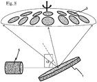
Figure 8 is a particle bombardment installation. -
Figures 9a to 9d depict the different stages for desired thicknesses determination for each target zone. -
Figure 10a depicts a stratified target intended for the application of a target structure determination optical process. -
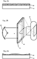
Figure 10b depicts a device intended to obtain target thicknesses. -
Figure 11a depicts components for the invention fungible element fabrication. -
Figure 11b depicts a section cut of an installation for the fabrication of the invention fungible element. - As can be appreciated in the figures, the invention refers to a
fungible element 1 provided with atarget 2 for the particle bombardment, intended to carry out the vapour-phase physical deposition of a thin layer on a substrate 3, saidfungible element 1 comprising abase layer 4 on which thetarget 2 is deposited, said target intended to be sputtered by the particle bombardment, wherein the target is formed by at least onelayer 21 in which a plurality of zones (xi, yi) is defined, having an average thickness (ej(xi, yi)) that is variable between the zones (xi , yi), said average thicknesses (ej(xi, yi)) of each zone (xi, yi) being dimensioned such that, in certain bombardment conditions, all the zones (xi , yi) have an identical ion sputtering time (tj). - This is illustrated in a very simplified way in
figure 5 . Here one can appreciate two different thickness zones e1 and e2 , which are submitted to different bombardment intensities. The element has been depicted in a convex shape, although it is not necessary to be shaped like this, for it will depend on the source yield distribution and the target yield distribution. - Another resulting distribution could be the one showed in
figure 7 . In some cases, especially when symmetries can be found in the installation different components and in the relative disposition between them, thickness distribution on the target will be approximate using a curve or a simple surface. - As can be appreciated in
figures 3, 4 and 6 , the target is formed by a plurality oflayers figures 2 and 3 , or heterogeneous as well as depicted infigures 4 and 5 . - The invention, as illustrated in
figure 8 , also refers to a set formed byparticle bombardment device 5 andfungible element 1 provided with atarget 2 to be bombarded (with ions, neutral particles or photons) by theparticle bombardment device 5 to perform vapour-phase physical deposition of a thin layer on a substrate 3 bound to receive the deposition material disposed on thetarget 2, saidfungible element 1 comprising abase layer 4 on which saidtarget 2 is deposited, characterized by the fact that saidtarget 2 is constituted by at least onelayer 21 in which a plurality of zones (xi , yi) with an average thickness (ej(xi, yi)) that is variable between the zones (xi, yi), said average thicknesses (ej(xi, yi)) of each zone (xi, yi) being dimensioned such that, in certain bombardment conditions, all the zones (xi , yi) have an identical ion sputtering time (tj), being so that the thickness of the layer deposited on said substrate 3 can be controlled by the previous sizing of thetarget 2 deposition material thicknesses (ej(xi, yi)). - The bombardment is an ionic bombardment performed by means of a cathodic sputtering head or a plasma ion gun as well as a bombardment of neutral particles by means of a neutralized ion gun or a plasma gun.
The bombardment can also be a photonic bombardment in order to produce laser ablation (LAD) or photonic bombardment by means of pulsed laser (PLD). - As an advantageous option, the head or
gun 5 comprises the means for changing its orientation so it is possible to orient it towards the target as well as the substrate, thus having the possibility of commuting between an ion or plasma gun assisted deposition mode and a compaction by direct bombardment mode. - The invention also refers to a process for the determination of an engraving pattern by
target 2 particles bombardment, in order to obtain an engraving velocity and thickness (ej(xi, yi)) based on the position (x, y) of afungible element 1 according to any of the variants depicted infigures 1 to 7 , comprising the stages of: - a) Perform an homogeneous deposit of deposition material on a
base layer 4 to obtain a known e0homogeneous thickness target 2, as shown infigure 9a ; - b) Dispose on the target 2 a resin mask 6, as depicted like a mesh in
figure 1 , so that there are zones of thetarget 2 that remain covered by the resin as well as zones that remain uncovered by theresin 7, as shown infigure 9b ; - c) Dispose the resulting product during a certain amount of time, in a certain position and in front of a certain
particle bombardment device 5 to perform a vapour-phase physical deposition process of a thin layer on a substrate 3, as depicted infigure 8 , so that a target like the one depicted infigure 9c can be obtained; - d) Remove the resin mask 6, i.e. by dissolution, in order to obtain the product depicted in
figure 9d ; - e) Measure the local height differences between
target 2 resin covered points and non resin coveredpoints 7, which is possible using the target depited infigure 9d ; - f) Obtain an engraving velocity function vj(xi, yi ) of the target (2) for the aforementioned certain conditions;
- g) Use the said engraving velocity function vj(xi, yi ) to determine the thickness (ej(xi, yi)) of the target in every position (x,y) so that the layer or layers (j) of the fungible element can be consumed one after another.
- An optical process with similar results can be performed following the stages of:
- a) Perform a deposition, distinguished by a certain optical absorption, α(λ), where λ is the wavelength, over a
transparent base layer 43 in order to obtain anhomogeneous thickness target 23, distinguished by a certain optical absorption, α(λ), as depicted infigure 10a ; - b) Dispose the
transparent base layer 43 with thehomogeneous thickness target 23, distinguished by a certain optical absorption, α(λ), in an l0 intensity, normal incidence illumination device with alamp 53, i.e. with white light or monochromatic light of l0 intensity, as depicted infigure 10b ; - c) Obtain a photographic image by means of a
photographic device 63, of the posterior part of the system integrated by thetransparent base 43 and thehomogeneous thickness target 23 and α(λ) optical absorption, when crossed by an incident light beam of l0 intensity, which is partially absorbed according to Alambert law:
transparent base 43 and thehomogeneous thickness target 23 and α(λ) optical absorption, where the variables (x, y) are thetarget 23 coordinates, and e(x,y) the thickness of thetarget 23 in every position after the sputtering by particle bombardment; - d) Dispose the product obtained in a) during a certain amount of time, in a certain position and in front of a certain
particle bombardment device 5 to carry out the vapour-phase physical deposition of a thin layer on a substrate 3, as shown infigure 8 , in such a way that a target like the one depicted infigure 9c is obtained; - e) Determine the relation IF(x,y)/IF 0(x,y) point by point, of the given intensity in every pixel of the
target 2 photographic images, before, IF 0(x,y), and after, IF(x,y), the particle bombardment by sputtering, performed for example by means of image treatment common techniques as well as techniques of matrix calculation using the image pixels as matrix elements. - f) Assuming the linearity of the photographic image collected intensities regarding the light beam intensity:

target 24 thickness after being sputtered by the particle bombardment, based on position (x,y) using the expression:
- g) Obtain an engraving velocity function v(x, y) for the
target 24 for the aforementioned certain conditions; - h) Use the engraving velocity function v(x, y) to determine the thickness e(x, y) of every target position (x,y) so that the layer or layers of the fungible element can be consumed one after another.
- i) Utilize image treatment software for, by means of the appropriate filters and the obtained thickness function e(x, y), and generate constant thickness domains Di ,ej(xi, yi) and arbitrary dimensions, that cover the
target 24 surface. - These processes can be performed in a systematic way, that is they can easily become a protocol or even be automated.
- The invention also refers to a process to fabricate the
fungible element 1, after the determination of the engraving velocity vi(xi,yi), by means of physical vapour deposition (PVD) techniques or chemical vapour deposition (CVD) techniques, to obtain monolayer or multilayer structures on abase layer 45, as shown infigure 11a , which comprises the stages of: - a) Perform a PVD or CVD deposition using a
mask 75, with a Di domain sized aperture, attached on abase layer 45, with adjustable (x, y) position, in order to obtain a monolayer ormultilayer target 25 with ej(xi, yi) thickness domains, as shown infigure 11b ; - b) Perform the material deposition in order to obtain a monolayer or
multilayer target 25 by means of PVD or CVD process, using amask 75 attached to thebase layer 45, sequentially by moving the base 45 over every Di domain, and keeping on the deposition process over every Di domain during a τij(xi, yi), time period, determined by the following expression:
target 25 multilayer system, by the PVD or CVD process conditions of each layer of thetarget 25 multilayer system and the final thicknesses of each desired material layer and the initial thickness obtained during the process of determination of the particle bombardment engraving pattern, where the subscripts i and j indicate respectively the domain and the multilayer system layer number to be obtained for thetarget 25 fabrication. - c) For the calculation of the constants Pij, Mij y Lij , a PVD or CVD deposition velocity calibration process is performed for each material to be used.
- The invention is not limited to the specific embodiments previously described but also comprises, for example, the variants that can be performed by the skilled person, always remaining within the scope of the claims.
Claims (20)
- The invention relates to a fungible element (1) provided with a target (2) for the particle bombardment, intended to carry out the vapour-phase physical deposition of a thin layer on a substrate (3), said fungible element (1) comprising a base layer (4) on which the target (2) is deposited, said target intended to be sputtered by the particle bombardment, wherein the target is formed by at least one layer (21) in which a plurality of zones (xi , yi ) is defined, having an average thickness (ej(xi, yi)) that is variable between the zones (xi , yi), said average thicknesses (ej(xi, yi)) of each zone (xi , yi ) being dimensioned such that, in certain bombardment conditions, all the zones (xi , yi ) have an identical ion sputtering time (tj).
- Element, according to claim number 1, wherein the target is constituted by a plurality of layers (21, 22).
- The element different zones (xi , yi), according to any of the previous claims, can be composed by the same material as well as by different materials.
- Set formed by particle bombardment device (5) and fungible element (1) provided with a target (2) to be bombarded by the particle bombardment device (5) to perform vapour-phase physical deposition of a thin layer on a substrate (3) bound to receive the deposition material disposed on the target (2), said fungible element (1) comprising a base layer (4) on which said target (2) is deposited, wherein said target (2) is constituted by at least one layer (21) in which a plurality of zones (xi , yi) with an average thickness (ej(xi, yi)) that is variable between the zones (xi, yi), said average thicknesses (ej(xi, yi)) of each zone (xi , yi) being dimensioned such that, in certain bombardment conditions, all the zones (xi, yi) have an identical ion sputtering time (tj), being so that the thickness of the layer deposited on said substrate (3) can be controlled by the previous sizing of the target (2) deposition material thicknesses (ej(xi, yi)).
- Said set, according to claim number 1, wherein the target is constituted by a plurality of layers (21, 22).
- Said set, according to any of claims 4 and 5, in its different zones (xi , yi) can be composed by the same material as well as by different materials.
- Said set, according to any of claims 4 to 6, in which the bombardment is an ionic bombardment performed by means of a cathodic sputtering head or a plasma ion gun as well as a bombardment of neutral particles by means of a neutralized ion gun or a plasma gun.
- Said set, according to any of claims 4 to 6, in which the bombardment is a photonic bombardment in order to produce laser ablation (LAD) or photonic bombardment by means of pulsed laser (PLD).
- Said set, according to claim number 7, in which the head or gun comprises the means for changing its orientation so it is possible to orient it towards the target as well as the substrate, thus having the possibility of commuting between an ion or plasma gun assisted deposition mode and a compaction by direct bombardment mode.
- Process for the determination of an engraving pattern by target (2) particles bombardment, in order to obtain an engraving velocity and thickness (ej(xi, yi)) based on the position (x, y) of a fungible element (1) according to any of claims 1 to 3, comprising the stages of:a) Perform an homogeneous deposit of deposition material on a base layer (4) to obtain an homogeneous thickness target (2);b) Dispose on the target (2) a resin mask (6), so that there are zones of the target (2) that remain covered by the resin as well as zones that remain uncovered by the resin (7);c) Dispose the resulting product during a certain amount of time, in a certain position and in front of a certain particle bombardment device (5) to perform a vapour-phase physical deposition process of a thin layer on a substrate (3);d) Remove the resin mask (6);e) Measure the local height differences between target (2) resin covered points and non resin covered points (7);f) Obtain an engraving velocity function vj(xi, yi) of the target (2) for the aforementioned certain conditions;g) Use the said engraving velocity function vj(xi, yi) to determine the thickness (ej(xi, yi)) of the target in every position (x,y) so that the layer or layers (j) of the fungible element can be consumed one after another.
- Process according to claim number 10, in which the mask (7) is a mesh.
- Process for the determination of the pattern by target (2) particles bombardment, for the obtaining of the engraving velocity and thickness (ej(xi, y)) based on the position (x, y) of a fungible element (1) according to any of claims 1 to 3, comprising the stages of:a) Perform a deposition, distinguished by a certain optical absorption, α(λ), where λ is the wavelength, over a transparent base layer (43) in order to obtain an homogeneous thickness target (23), distinguished by a certain optical absorption, α(λ);b) Dispose the transparent base layer (43) with the homogeneous thickness target (23), distinguished by a certain optical absorption, α(λ), in an l0 intensity, normal incidence illumination device with a lamp (53);c) Obtain a photographic image by means of a photographic device (63), of the posterior part of the system integrated by the transparent base (43) and the homogeneous thickness target (23) and α(λ) optical absorption, when crossed by an incident light beam of l0 intensity, which is partially absorbed according to Alambert law:
 d) Dispose the product obtained in a) during a certain amount of time, in a certain position and in front of a certain particle bombardment device (5) to carry out the vapour-phase physical deposition of a thin layer on a substrate (3);e) Determine the relation IF(x,y)/IF 0(x,y) point by point, of the given intensity in every pixel of the target (2) photographic images, before, IF 0(x,y), and after, IF(x,y), the particle bombardment by sputtering.f) Assume the linearity of the photographic image collected intensities regarding the light beam intensity:
 g) Obtain an engraving velocity function v(x, y) for the target (24) for the aforementioned certain conditions;h) Use the engraving velocity function v(x, y) to determine the thickness e(x, y) of every target position (x,y) so that the layer or layers of the fungible element can be consumed one after another.i) Utilize image treatment software for, by means of the appropriate filters and the obtained thickness function e(x, y), and generate constant thickness domains Di , ej(xi, yi) and arbitrary dimensions, that cover the target (24) surface.
 - Process, according to claim number 12, in which the deposition of stage a) is homogeneous and formed by a semitransparent deposition material.
- Process, according to claim 13, in which the deposition is a very thin metal layer of about some tens of nanometers, as well as a semitransparent material with a non null optical transmittance specter, such as a semiconductor material, or a semitransparent dielectric.
- Process, according to claims 12 to 14, in which the stage b) is performed with white light or monochromatic light of l0 intensity.
- Process, according to any claim from 1 to 15, in which stage e) is performed by means of image treatment common techniques as well as techniques of matrix calculation using the image pixels as matrix elements.
- Process to fabricate the fungible element (1), after the determination of the engraving velocity vi(xi , yi), by means of physical vapour deposition (PVD) techniques or chemical vapour deposition (CVD) techniques, to obtain monolayer or multilayer structures on a base layer (45), which comprises the stages of:a) Perform a PVD or CVD deposition using a mask (75), with a Di domain sized aperture, attached on a base layer (45), with adjustable (x, y) position, in order to obtain a monolayer or multilayer target (25) with ej(xi, yi) thickness domains;b) Perform the material deposition in order to obtain a monolayer or multilayer target (25) by means of PVD or CVD process, using a mask (75) attached to the base layer (45), sequentially by moving the base (45) over every Di domain, and keeping on the deposition process over every Di domain during a τij(xi, yi), time period, determined by the following expression:

- Process, according to claim number 17, in which the mask (75) is formed by a rigid material, preferably metallic.
- Process, according to claim 17 or 18, in which a single process or a repetitive process is performed in the stage b).
- Process, according to any of the claims 17 to 19, in which for the calculation of the constants Pij, Mij y Lij, a PVD or CVD deposition velocity calibration process is performed for each material to be used.
Applications Claiming Priority (2)
| Application Number | Priority Date | Filing Date | Title |
|---|---|---|---|
| ES201530440A ES2584961B1 (en) | 2015-03-31 | 2015-03-31 | Fungible element for particle bombardment and etching determination procedure of said element |
| PCT/ES2016/070220 WO2016156649A1 (en) | 2015-03-31 | 2016-03-30 | Perishable element for particle bombardment, set of devices for particle bombardment and perishable element and method for determining the etching pattern via particle bombardment of a target |
Publications (2)
| Publication Number | Publication Date |
|---|---|
| EP3279365A1 true EP3279365A1 (en) | 2018-02-07 |
| EP3279365A4 EP3279365A4 (en) | 2019-03-20 |
Family
ID=56979843
Family Applications (1)
| Application Number | Title | Priority Date | Filing Date |
|---|---|---|---|
| EP16771450.0A Withdrawn EP3279365A4 (en) | 2015-03-31 | 2016-03-30 | FUNGAL MEMBER FOR PARTICULAR BOMBARDMENT, PARTICULAR BOMBARDMENT DEVICE AND FIBERABLE MEMBER, AND METHOD FOR DETERMINING THE ENGRAVING MODEL BY BOMBING A TARGET WITH PARTICLES |
Country Status (4)
| Country | Link |
|---|---|
| US (1) | US20180073133A1 (en) |
| EP (1) | EP3279365A4 (en) |
| ES (1) | ES2584961B1 (en) |
| WO (1) | WO2016156649A1 (en) |
Cited By (1)
| Publication number | Priority date | Publication date | Assignee | Title |
|---|---|---|---|---|
| EP4019663A1 (en) * | 2020-12-23 | 2022-06-29 | Advanced Nanotechonologies, S.L. | Installation for depositing nanostructures on a substrate |
Families Citing this family (3)
| Publication number | Priority date | Publication date | Assignee | Title |
|---|---|---|---|---|
| US11049697B2 (en) | 2018-06-20 | 2021-06-29 | Board Of Trustees Of Michigan State University | Single beam plasma source |
| TWI707055B (en) * | 2019-03-12 | 2020-10-11 | 永合益科技股份有限公司 | Image-data based automatically controlling pvd system and method of the same |
| WO2020198012A1 (en) | 2019-03-26 | 2020-10-01 | Board Of Trustees Of Michigan State University | Single beam plasma source |
Family Cites Families (9)
| Publication number | Priority date | Publication date | Assignee | Title |
|---|---|---|---|---|
| US5830327A (en) * | 1996-10-02 | 1998-11-03 | Intevac, Inc. | Methods and apparatus for sputtering with rotating magnet sputter sources |
| JP2004514066A (en) * | 2000-11-27 | 2004-05-13 | ユナキス・トレーディング・アクチェンゲゼルシャフト | RF magnetron target with reduced thickness |
| TWI224626B (en) * | 2001-04-24 | 2004-12-01 | Tosoh Smd Inc | Method of optimizing a sputtering target profile for the purpose of extending target utilization life and targets made by such method |
| KR20030071926A (en) * | 2002-03-02 | 2003-09-13 | 엘지.필립스 엘시디 주식회사 | Sputtering target assembly and sputtering apparatus using the same |
| US20110303535A1 (en) * | 2007-05-04 | 2011-12-15 | Miller Steven A | Sputtering targets and methods of forming the same |
| KR20150128817A (en) * | 2007-12-21 | 2015-11-18 | 사푸라스트 리써치 엘엘씨 | Method for sputter targets for electrolyte films |
| US8053861B2 (en) * | 2009-01-26 | 2011-11-08 | Novellus Systems, Inc. | Diffusion barrier layers |
| CN101921989A (en) * | 2010-06-30 | 2010-12-22 | 昆山工研院新型平板显示技术中心有限公司 | Method for improving utilization rate of target of sputtering technology |
| TWI605142B (en) * | 2013-01-04 | 2017-11-11 | 塔沙Smd公司 | Silicon sputtering target with enhanced surface profile and improved performance and methods of making the same |
-
2015
- 2015-03-31 ES ES201530440A patent/ES2584961B1/en not_active Expired - Fee Related
-
2016
- 2016-03-30 WO PCT/ES2016/070220 patent/WO2016156649A1/en not_active Ceased
- 2016-03-30 EP EP16771450.0A patent/EP3279365A4/en not_active Withdrawn
- 2016-03-30 US US15/563,856 patent/US20180073133A1/en not_active Abandoned
Cited By (2)
| Publication number | Priority date | Publication date | Assignee | Title |
|---|---|---|---|---|
| EP4019663A1 (en) * | 2020-12-23 | 2022-06-29 | Advanced Nanotechonologies, S.L. | Installation for depositing nanostructures on a substrate |
| WO2022136400A1 (en) * | 2020-12-23 | 2022-06-30 | Advanced Nanotechnologies S.L. | Installation for depositing nanostructures on a substrate |
Also Published As
| Publication number | Publication date |
|---|---|
| ES2584961B1 (en) | 2017-07-04 |
| ES2584961A1 (en) | 2016-09-30 |
| WO2016156649A1 (en) | 2016-10-06 |
| EP3279365A4 (en) | 2019-03-20 |
| US20180073133A1 (en) | 2018-03-15 |
Similar Documents
| Publication | Publication Date | Title |
|---|---|---|
| US20180073133A1 (en) | Perishable element for particle bombardment, set of devices for particle bombardment and perishable element and method for determining the etching pattern via particle bombardment of a target | |
| JP6925358B2 (en) | Atomic layer deposition process for producing dielectric metasurfaces for wavelengths in the visible spectrum | |
| Veiko et al. | Laser coloration of titanium films: New development for jewelry and decoration | |
| Murthy et al. | Plasmonic color metasurfaces fabricated by a high speed roll-to-roll method | |
| BE1021296B1 (en) | SPUTTER SYSTEM FOR UNIFORM SPUTTERING | |
| Andreazza et al. | Nucleation and initial growth of platinum islands by plasma sputter deposition | |
| US20180265998A1 (en) | Multi-material light-directed electrophoretic deposition and electroplating over large areas using moveable projected images and/or electrodes | |
| Rodríguez et al. | Plasmonic response and transformation mechanism upon single laser exposure of metal discontinuous films | |
| Sayin et al. | Formation of charge-nanopatterned templates with flexible geometry via layer by layer deposition of polyelectrolytes for directed self-assembly of gold nanoparticles | |
| Do et al. | Nano-patterning of gold thin film by thermal annealing combined with laser interference techniques | |
| Takáts et al. | Diffusion induced atomic islands on the surface of Ni/Cu nanolayers | |
| AU746370B2 (en) | Distribution mask for depositing by vacuum evaporation | |
| JP2003155556A (en) | Manufacturing method of wedge-shaped film | |
| Liese et al. | Development of laser deposited multilayer zone plate structures for soft X-ray radiation | |
| Baum et al. | Generation of phase-only holograms by laser ablation of nanoparticulate ITO layers | |
| Boher et al. | Interface analysis of sputtered WC, Rh-C and Ni-C multilayers for soft x-ray applications | |
| García-Valenzuela et al. | 2D compositional self-patterning in magnetron sputtered thin films | |
| Weppelman et al. | Fabrication of narrow-gap nanostructures using electron-beam induced deposition etch masks | |
| CA2983683A1 (en) | Spectral gradient filter production using surface applied array optimized 3d shadow masks | |
| Guilfoyle et al. | Modelling of pulsed laser deposition of large area films | |
| DE202023104857U1 (en) | Magnetron sputtering and electron beam evaporation composite coating machine | |
| Seo et al. | Mass printing of colored natural patterns on Al plate by roll imprinting and thin film deposition | |
| US20040063226A1 (en) | Growth of multi-component alloy films with controlled graded chemical composition on sub-nanometer scale | |
| Lochbihler et al. | Complementary aluminum nanopatch/nanohole arrays for broad palettes of colors | |
| CN109071326A (en) | The coating product and/or its production method of the metal island layer to be formed are controlled including the use of temperature |
Legal Events
| Date | Code | Title | Description |
|---|---|---|---|
| STAA | Information on the status of an ep patent application or granted ep patent |
Free format text: STATUS: THE INTERNATIONAL PUBLICATION HAS BEEN MADE |
|
| PUAI | Public reference made under article 153(3) epc to a published international application that has entered the european phase |
Free format text: ORIGINAL CODE: 0009012 |
|
| STAA | Information on the status of an ep patent application or granted ep patent |
Free format text: STATUS: REQUEST FOR EXAMINATION WAS MADE |
|
| 17P | Request for examination filed |
Effective date: 20171031 |
|
| AK | Designated contracting states |
Kind code of ref document: A1 Designated state(s): AL AT BE BG CH CY CZ DE DK EE ES FI FR GB GR HR HU IE IS IT LI LT LU LV MC MK MT NL NO PL PT RO RS SE SI SK SM TR |
|
| AX | Request for extension of the european patent |
Extension state: BA ME |
|
| DAV | Request for validation of the european patent (deleted) | ||
| DAX | Request for extension of the european patent (deleted) | ||
| RIC1 | Information provided on ipc code assigned before grant |
Ipc: C23C 14/34 20060101AFI20181113BHEP Ipc: H01J 37/34 20060101ALI20181113BHEP |
|
| A4 | Supplementary search report drawn up and despatched |
Effective date: 20190219 |
|
| RIC1 | Information provided on ipc code assigned before grant |
Ipc: C23C 14/34 20060101AFI20190213BHEP Ipc: H01J 37/34 20060101ALI20190213BHEP |
|
| RAP1 | Party data changed (applicant data changed or rights of an application transferred) |
Owner name: UNIVERSITAT DE BARCELONA Owner name: ADVANCED NANOTECHONOLOGIES, S.L. |
|
| STAA | Information on the status of an ep patent application or granted ep patent |
Free format text: STATUS: EXAMINATION IS IN PROGRESS |
|
| 17Q | First examination report despatched |
Effective date: 20210302 |
|
| STAA | Information on the status of an ep patent application or granted ep patent |
Free format text: STATUS: THE APPLICATION IS DEEMED TO BE WITHDRAWN |
|
| 18D | Application deemed to be withdrawn |
Effective date: 20210914 |