EP3276831A1 - Self-limiting electrical triggering for initiating fracture of frangible glass - Google Patents
Self-limiting electrical triggering for initiating fracture of frangible glass Download PDFInfo
- Publication number
- EP3276831A1 EP3276831A1 EP17182802.3A EP17182802A EP3276831A1 EP 3276831 A1 EP3276831 A1 EP 3276831A1 EP 17182802 A EP17182802 A EP 17182802A EP 3276831 A1 EP3276831 A1 EP 3276831A1
- Authority
- EP
- European Patent Office
- Prior art keywords
- self
- glass substrate
- temperature
- limiting
- resistive element
- Prior art date
- Legal status (The legal status is an assumption and is not a legal conclusion. Google has not performed a legal analysis and makes no representation as to the accuracy of the status listed.)
- Granted
Links
Images




Classifications
-
- H—ELECTRICITY
- H01—ELECTRIC ELEMENTS
- H01H—ELECTRIC SWITCHES; RELAYS; SELECTORS; EMERGENCY PROTECTIVE DEVICES
- H01H85/00—Protective devices in which the current flows through a part of fusible material and this current is interrupted by displacement of the fusible material when this current becomes excessive
- H01H85/0039—Means for influencing the rupture process of the fusible element
- H01H85/0047—Heating means
- H01H85/0052—Fusible element and series heating means or series heat dams
-
- H—ELECTRICITY
- H03—ELECTRONIC CIRCUITRY
- H03K—PULSE TECHNIQUE
- H03K19/00—Logic circuits, i.e. having at least two inputs acting on one output; Inverting circuits
- H03K19/02—Logic circuits, i.e. having at least two inputs acting on one output; Inverting circuits using specified components
- H03K19/173—Logic circuits, i.e. having at least two inputs acting on one output; Inverting circuits using specified components using elementary logic circuits as components
- H03K19/177—Logic circuits, i.e. having at least two inputs acting on one output; Inverting circuits using specified components using elementary logic circuits as components arranged in matrix form
- H03K19/17748—Structural details of configuration resources
- H03K19/17768—Structural details of configuration resources for security
-
- H—ELECTRICITY
- H10—SEMICONDUCTOR DEVICES; ELECTRIC SOLID-STATE DEVICES NOT OTHERWISE PROVIDED FOR
- H10W—GENERIC PACKAGES, INTERCONNECTIONS, CONNECTORS OR OTHER CONSTRUCTIONAL DETAILS OF DEVICES COVERED BY CLASS H10
- H10W42/00—Arrangements for protection of devices
- H10W42/40—Arrangements for protection of devices protecting against tampering, e.g. unauthorised inspection or reverse engineering
-
- H—ELECTRICITY
- H10—SEMICONDUCTOR DEVICES; ELECTRIC SOLID-STATE DEVICES NOT OTHERWISE PROVIDED FOR
- H10P—GENERIC PROCESSES OR APPARATUS FOR THE MANUFACTURE OR TREATMENT OF DEVICES COVERED BY CLASS H10
- H10P54/00—Cutting or separating of wafers, substrates or parts of devices
Definitions
- This invention relates to transient electronics, and in particular to trigger devices and triggering methods utilized to initiate the fragmentation of frangible glass substrates in transient electronic assemblies.
- transient electronics refers to a relatively new family of electronic devices that disappear (disaggregate and disperse) within a set period of time, making them ideally suited for distributed network systems.
- Conventional transient electronic systems typically rely on the use of soluble substrates and electronic materials (such as silk). When placed into solvent (typically water), these conventional substrates and electronics slowly dissolve into solution. As such, a distributed network system made up of conventional transient electronic devices can be expected to "disappear" over a relatively short amount of time (e.g., after periodic rainfall).
- transient electronic device in which functional circuitry fabricated using well-known low-cost fabrication techniques (e.g., CMOS or SOI) and disposed on a frangible glass substrate that, when subjected to a small initial fracture force, underwent complete disaggregation (shattering) in a manner that releases sufficient potential energy to also cause disaggregation of the functional circuitry.
- the transient event i.e., disaggregation
- resistive heating type trigger mechanisms may require a pulse shaping circuit configured to generate and transmit a shaped current pulse from a power source to the resistive heating element in order to generate initial fracture.
- the present invention is directed to a simple and reliable trigger mechanism and associated triggering method for reliably initiating powerderization of functional circuitry (electronic elements) in a transient electronic device by way of generating a localized thermal pulse (i.e., rapid heating followed by rapid cooling) using a self-limiting circuit arrangement that avoids the need for current pulse shaping circuitry and/or complicated connection arrangements, thereby avoiding the problems associated with conventional approaches.
- a localized thermal pulse i.e., rapid heating followed by rapid cooling
- the trigger mechanism includes a self-limiting resistive element that is at least partially formed on a frangible glass substrate.
- the frangible glass substrate is constructed substantially entirely from a glass material having an associated melting point temperature using known techniques such that it undergoes complete disaggregation (shattering) in response to an applied initial fracture force.
- the electronic elements e.g., a silicon-on-insulator-based (SOI-based) IC, a chip-based IC, or thin-film electronics patterned directly onto the frangible glass substrate
- the self-limiting resistive element of the trigger mechanism are fixedly attached to one or both surfaces of the frangible glass substrate, with the electronic elements typically dispose over a first region of the frangible glass substrate, and the self-limiting resistive element disposed over a localized (i.e., relatively small) second region of the frangible glass substrate.
- the localized thermal pulse generated by the self-limiting resistive element produces a stress profile caused by rapid heating above the glass' melting point temperature and then cooling in the localized region located adjacent (e.g., below) the self-limiting resistive element.
- the resulting stress profile generates the desired initial fracture force in the localized region, thereby initiating the complete disaggregation of the frangible glass substrate, along with the electronic elements disposed thereon.
- the self-limiting resistive element includes a current-limiting portion (e.g., a fuse, timer-based or thermistor-based circuit) that independently controls (i.e., without requiring an externally-generated control signal) an amount generated heat by way of terminating the flow of a trigger current through the self-limiting resistive element after a predetermined amount of generated heat is transmitted into the localized region of the frangible glass substrate.
- the current-limiting portion is implemented by a fuse structure that is configured to melt/break after a predetermined amount of heat is generated by the self-limiting resistive element, thereby producing an open circuit that terminates further heat generation by way of preventing further trigger current flow through the self-limiting resistive element.
- the self-limiting resistive element provides a simple and reliable mechanism for generating the desired thermal pulse and resulting stress profile that produce the initial fracture force in the localized region of the frangible glass substrate.
- the self-limiting resistive element facilitates electronic control of the triggering event using very simple addressing electronics, thereby minimizing system complexity. That is, because the self-limiting resistive element eliminates the need for current shaping electronics, the trigger mechanism is able to achieve complete, on-command disaggregation of the electronic circuitry formed on the frangible glass substrate using a simple switch element that is controllable (i.e., actuated to generate the trigger current) by way of an electronic trigger signal to selectively couple the self-limiting resistive element to a direct-current (DC) power source (e.g., a battery).
- DC direct-current
- the switch element is turned on at the beginning of a transient event in response to the electronic trigger signal, thereby initiating a large direct current (i.e., the trigger current) to flow from the DC power source through the self-limiting resistive element, whereby the self-limiting resistive element operates as described above to generate the thermal pulse resulting in the initial fracture force causing disaggregation of the frangible glass substrate.
- the triggering mechanism of the present invention is simple and reliable, thereby reducing manufacturing costs and complexity.
- the self-limiting resistive element is configured to generate resistive heat (i.e., by way of passing the large trigger current through one or more resistor structures) for a predetermined amount of time after actuation of the switch element, whereby a temperature of the localized region of the frangible glass substrate rapidly increases from a relatively low initial temperature (e.g., approximately 140°C) to a high (first) temperature level temperature (e.g., approximately 220°C) that is above the melting point temperature of the glass forming the frangible glass substrate.
- a relatively low initial temperature e.g., approximately 140°C
- a high (first) temperature level temperature e.g., approximately 220°C
- the self-limiting resistive element is further configured to independently control the amount of generated heat by way of terminating the flow of trigger current through the resistor element(s) at the end of the predetermined time period, whereby terminating the heat generating process causes rapid cooling of the localized region (e.g., from the high (first) temperature (e.g., 220°C) to a lower (second) temperature (e.g., approximately 200°C), e.g., in approximately one second) by way of heat dissipation from the localized region into surrounding substrate regions.
- first first
- second temperature e.g., approximately 200°C
- the present inventors determined that a thermal pulse generated in this manner produces a stress profile that reliably generates an initial fracture force in the localized region having sufficient strength to produce subsequent propagating fracture forces that pass throughout the frangible glass substrate, causing "powderization” (i.e., disaggregation or fragmentation) of the frangible glass substrate into micron-sized particulates.
- "powderization" i.e., disaggregation or fragmentation
- the present invention provides a low-cost and reliable triggering mechanism for initiating powderization of electronic elements disposed on a transient electronic device.
- the self-limiting resistive element is entirely formed by a resistive material that is deposited and patterned directly onto a surface of the frangible glass substrate using a standard thin-film fabrication technique (e.g., photolithographic or inkjet printing).
- the resistive material includes magnesium, copper, tungsten, aluminum, molybdenum or chrome, or a combination of one or more of these metals.
- Other suitable materials may also be used, provided the material is sufficiently conductive and adheres to the frangible glass substrate surface well enough that heat is transferred efficiently into the localized region during the rapid heating portion of the thermal pulse.
- the self-limiting resistive element includes one or more resistive portion connected in series with the current-limiting portion between two (first and second) terminals, with the first terminal is coupled by way of the switch element to the direct current (DC) power source and the second terminal connected to a suitable ground structure.
- the resistive material mentioned above is patterned to form two relatively large resistor structures connected by a narrow fuse element, where the resistor structures are configured to heat up but remain coherent during the thermal pulse, and the fuse element is configured to melt and break at the end of the rapid heating (first) time period.
- a fuse element to implement the current-control portion of the self-limiting resistive element provides a low-cost, simple and highly reliable structure for independently controlling the amount of heat generated during the rapid heating process, and reliably produces an open circuit condition (i.e., by way of melting/breaking) that terminates flow of the trigger current through the resistor structures at the start of the rapid cooling portion of the thermal pulse.
- the resistive material utilized to form the self-limiting resistive element is patterned into a bowtie-type structure in which the two resistor structures including respective downward-tapered sections, and the fuse element is formed by a narrow section of resistive material connected between tapered ends of the downward-tapered sections.
- the fuse element includes a straight rectangular structure extending between the tapered end, and in another embodiment the narrow resistive material section forming the fuse element is disposed in a substantially S-shaped pattern. In either case, a width W of the narrow resistive material section is greater than a thickness of the frangible glass substrate determines to induce reliable disaggregation.
- the narrow resistive material section forming the fuse element has a width of at least 0.3 mm.
- resistor structures can have almost any size, although while larger resistors ensure reliable fragmentation, they also require more power and energy from the power source. Accordingly, the smallest possible resistor structures are preferred in order to minimize power and energy requirements.
- the transient electronic device further includes a sensor configured to detect a transmitted wave signal (e.g., a light wave signal, a radio frequency (RF), or an acoustic/sound signal), and configured to then generate the electronic trigger signal used to actuate the switch element.
- a remote optical signal is detected by a photodiode (light wave sensor), whereby current through the photodiode causes a silicon controlled rectifier (switch element) to latch, which in turn couples a battery across the self-limiting resistor element, ultimately causing disaggregation (fragmentation) of the glass substrate and any included electronics.
- RF signals and acoustic wave signals may be utilized by replacing the photodiode with a radio-frequency wave sensor or an acoustic wave sensor.
- other physical and chemical stimuli may also be utilized in conjunction with an appropriate sensor to initiate a fragmentation sequence.
- latching is achieved using a silicon controlled rectifier, other switch elements may also be utilized, such as a single MOSFET transistor or a multiple-element latch circuit.
- one or more of the switch element and sensor utilized to control operation of the triggering mechanism may be formed/mounted directly on the frangible glass substrate, formed on a semiconductor layer/die on which the electronic elements are formed, or disposed on an external printed circuit board to which the transient electronic device is attached.
- the photodiode/sensor and the silicon controlled rectifier (switch) may be implemented by patterning suitable materials directly onto the frangible glass substrate, or may be implemented using CMOS fabrication techniques on a semiconductor structure (e.g., IC chip or SOI layer) on which the electronic elements are formed and that is fixedly attached to the frangible glass substrate.
- the frangible glass substrate comprises one of a stressed glass substrate including stress-engineered tensile and compressive layers that are operably attached together, a thermally tempered glass substrate including laminated layers of different glass types having associated different coefficient of thermal expansion (CTE) values, and an ion-exchange treated glass substrate.
- the frangible glass substrate contains enough stored energy to generate self-propagating secondary fractures in response to an initial fracture force such that the glass substrate completely disaggregates ("powderizes") into micron-sized particulates by way of a mechanism similar to that captured in a Prince Rupert's Drop.
- the electronic devices are either fabricated directly onto the frangible glass substrate using standard silicon-on-insulator (SOI) fabrication techniques (i.e., such that the functional circuitry is implemented as an SOI integrated circuit structure), or are separately fabricated on an IC die (chip) that is then attached to the frangible glass substrate using anodic bonding.
- SOI silicon-on-insulator
- the released potential energy during disaggregation of the frangible glass substrate is sufficient to also powderize the electronic devices, along with the trigger mechanism and any other structures that might be disposed on the frangible glass substrate.
- the present invention relates to an improvement in transient electronic devices.
- the following description is presented to enable one of ordinary skill in the art to make and use the invention as provided in the context of a particular application and its requirements.
- directional terms such as “upper”, “upward”, “lower”, “downward” and “over” are intended to provide relative positions for purposes of description, and are not intended to designate an absolute frame of reference.
- the terms “coupled” and “connected”, which are utilized herein, are defined as follows.
- the term “connected” is used to describe a direct connection between two circuit elements, for example, by way of a metal line formed in accordance with normal integrated circuit fabrication techniques.
- the term “coupled” is used to describe either a direct connection or an indirect connection between two circuit elements.
- two coupled elements may be directly connected by way of a metal line, or indirectly connected by way of an intervening circuit element (e.g., a capacitor, resistor, inductor, or by way of the source/drain terminals of a transistor).
- an intervening circuit element e.g., a capacitor, resistor, inductor, or by way of the source/drain terminals of a transistor.
- Fig. 1 includes simplified perspective views showing a transient electronic device 100 in a pre-transience "whole" state (i.e., device 100(t0) shown in the middle portion of Fig. 1 ) and a post-transience "powderized” state (i.e., device 100(t2) shown in the lower portion of Fig. 1 ).
- transient electronic device 100(t0) In the pre-transience state (e.g., immediately after production, during normal operation, and during portions of the transient event occurring prior to disaggregation), transient electronic device 100(t0) generally includes functional electronics 120 and a trigger mechanism 130 that are disposed over corresponding regions of frangible glass substrate 110.
- device 100(t2) at the bottom of Fig.
- frangible glass substrate and any structures disposed thereon i.e., functional electronics 120 and any portion of trigger mechanism 130 mounted on frangible glass substrate 110
- frangible glass substrate 110 in the post-transience "powerderized” state, the frangible glass substrate and any structures disposed thereon (i.e., functional electronics 120 and any portion of trigger mechanism 130 mounted on frangible glass substrate 110) are completely disaggregated (“powderized”) into micron-sized particulates 101 (i.e., have sizes ⁇ 100 ⁇ m across).
- frangible glass substrate 110 is a wafer-like structure having opposing upper and lower surfaces 111 and 112, and is constructed using known techniques such that it undergoes complete disaggregation (shattering) in response to the initial fracture force generated/applied by trigger mechanism 130.
- frangible glass substrate 110 includes at least one glass structure including a first glass material having a first coefficient of thermal expansion (CTE) value, and multiple second glass structures respectively including one or more different (second) glass materials respectively having a second CTE value, where the second CTE value is different from the first CTE value.
- thermally tempered glass substrate 110A includes a glass structure 110A-1 disposed between two glass structures 110A-21 and 110A-22, where glass structure 110A-1 comprises a different glass material having a different CTE value than the glass material from which glass structures 110A-21 and 110A-22 are formed.
- glass structure 110A-1 comprises a different glass material having a different CTE value than the glass material from which glass structures 110A-21 and 110A-22 are formed.
- thermally tempered glass substrate 110B includes (second) glass structures 110B-21, 110B-22 and 110B-23 disposed in a (first) glass structure 110B-1, where glass structure 110B-1 comprises a different glass material than that of glass structures 110B-21 to 110B-23.
- frangible glass substrate 110 comprises a stressed glass substrate including stress-engineered tensile and compressive layers that are operably attached together in the manner described in U.S. Patent No. 9,154,138 , which is also incorporated herein by reference in its entirety.
- frangible glass substrate 110 an ion-exchange treated glass substrate or interposer fabricated in the manner described in U.S. Pat. App. Ser. No. 14/694,132 filed 04/23/2015 and entitled "Transient Electronic Device With Ion-Exchanged Glass Treated Interposer” [Atty Dkt. No. 20141606US01/XCP-205] which is also incorporated herein by reference in its entirety.
- frangible glass substrate 110 contains enough stored energy to generate self-propagating secondary fractures in response to an initial fracture force such that, as depicted by device 100(t2) at the bottom of Fig.
- frangible glass substrate 110 completely disaggregates ("powderizes") into micron-sized particulates (i.e., ⁇ 100 ⁇ m across) using a mechanism similar to that captured in a Prince Rupert's Drop.
- the released potential energy during disaggregation of frangible glass substrate 110 is sufficient to also powderize functional electronics 120 as also illustrated by device 100(t2).
- the released potential energy also powderizes portions of trigger mechanism 130 and any other structures that might be disposed on frangible glass substrate 110.
- Functional electronics 120 include electronic elements 122 fabricated on a semiconductor base layer 121 (e.g., an SOI layer or an integrated circuit (IC) die/chip) that is fixedly attached to upper surface 111 and dispose over a corresponding region 110-1 of frangible glass substrate 110.
- a semiconductor base layer 121 e.g., an SOI layer or an integrated circuit (IC) die/chip
- transient electronics is to provide a way to essentially entirely eliminate an IC or other electronic elements for purposes of protecting the environment or maintaining confidentiality (i.e., preventing unauthorized reverse engineering of the elements/circuit).
- a benefit of fabricating transient electronic device 100 on frangible glass substrate 110 is that this approach both facilitates forming functional electronics 120 using low cost manufacturing techniques, and facilitates reliable elimination of functional electronics 120 by way of causing disaggregation of frangible glass substrate 110.
- functional electronics 120 are fabricated by way of forming electronic elements 122 on a suitable semiconductor (base) layer 121 using existing IC fabrication techniques (e.g., CMOS), and electronic elements 122 are configured to perform a prescribed useful function (e.g., sensor operations) up until the transient event.
- the semiconductor layer 121 is a silicon "chip" (die) upon which electronic elements 122 are fabricated, and then the semiconductor layer 121 is fixedly attached to glass substrate 110 using known die bonding techniques (e.g., anodic bonding or by way of sealing glass) that assure coincident powderization of electronic elements 122 with frangible glass substrate 110.
- functional electronics 120 includes electronic elements 122 configured to form an IC device using standard silicon-on-insulator (SOI) fabrication techniques (i.e., such that the functional circuitry is implemented as an SOI integrated circuit structure).
- SOI silicon-on-insulator
- functional electronics 120 are fabricated on an IC die that is "thinned" (e.g., subjected to chemical mechanical polishing) before the bonding process.
- trigger mechanism 130 is configured to generate an initial fracture force in frangible glass substrate 110 in response to an electronic trigger signal TS.
- trigger mechanism 130 achieves this function using a self-limiting resistive element 140 and a switch element 150 that are connected in series between a battery (or other DC power source PS) and ground.
- a self-limiting resistive element 140 and a switch element 150 that are connected in series between a battery (or other DC power source PS) and ground.
- at least a portion of trigger mechanism 130 is disposed on upper surface 111 over a second region 110-2 of frangible glass substrate 110 (i.e., away from functional circuitry 120), but may alternatively be formed on lower surface 112.
- Switch element 150 has a first terminal connected to battery PS, a second terminal connected to a first terminal 141-1 of element 140, and a control terminal operably disposed to receive electronic trigger signal TS, which may be generated by an optional sensor or other control circuitry (not shown). As set forth below, switch element 150 is actuated (switched from an open/nonconducting state to a closed/conducing state) at the start of a transient event by way of asserting trigger signal TS, whereby switch element 150 initiates a DC trigger current I T that flows from battery PS through self-limiting resistive element 140 to ground.
- TS electronic trigger signal
- self-limiting resistive element 140 includes a resistive portion 142 and a current-limiting portion 145 that are connected in series between battery PS and ground by way of a first terminal 141-1 and a second terminal 141-2, respectively, where at least one of resistive portion 142 and a current-limiting portion 145 are disposed on upper surface 111 over a localized (i.e., relatively small) region 111-21 of frangible glass substrate 110.
- resistive portion 142 and a current-limiting portion 145 are configured and operably thermally coupled to frangible glass substrate 110 such that self-limiting resistive element 140 generates heat at a rate that rapidly increases a localized temperature of localized region 110-21, and current limiting portion 145 is further configured to independently control (i.e., without requiring an externally-generated control signal) the flow of trigger current I T by way of terminating the flow of trigger current I T after localized region 110-21 receives a sufficiently large amount of the heat generated by self-limiting resistive element 140.
- current-limiting portion 145 is implemented by a fuse element configured to fail (melt and break) after conducting a predetermined amount of trigger current I T (i.e., after a predetermined amount of heat is generated by self-limiting resistive element 140).
- current-limiting portion 145 may be implemented by other elements/circuits configured to implement the described independent control over trigger current I T , such as a thermistor-based circuit configured to terminate the trigger current flow upon detecting a predetermined temperature level, or a timer-based circuit configured to terminate the trigger current flow a preset time after actuation of switch element 150.
- Fig. 2 is a flow diagram showing a generalized method for triggering a disaggregation event on transient electronic device 100 (shown in Fig. 1 ), and Figs. 3(A), 3(B), 3(C), 3(D), 3(E) and 3(F) are partial cross-sectional side views showing a portion of transient electronic device 100 before and during an exemplary disaggregation event.
- transient electronic device 100(t0) ( Fig. 1 ) is subjected to normal operation (i.e., functional circuitry 120 performs as intended).
- Fig. 3(A) is a simplified cross-section showing a portion of device 100(t0), where resistive portion 142 of self-limiting resistive element 140 is depicted as a metal structure disposed on upper surface 111 of the frangible glass substrate 110 over localized region 110-21, and current control portion 145 is depicted as a switch in a closed (i.e., conducting) state.
- switch portion 150 is open (i.e., in a nonconducting state), so no current passes from battery PS through self-limiting resistive element 140, and thus no heat is generated by resistive portion 142. Accordingly, at time t0, a localized temperature T LR in localized region 110-21 assumes the same (relatively low) initial temperature To as that of surrounding adjacent regions 100-22 of frangible glass substrate 110.
- the transient event is initiated at a time t10, for example, when a trigger event signal is detected by a sensor (e.g., in response to a wirelessly transmitted light or RF signal), or unauthorized tampering is detected.
- a trigger event signal is detected by a sensor (e.g., in response to a wirelessly transmitted light or RF signal), or unauthorized tampering is detected.
- trigger signal TS ( Fig. 1 ) is asserted and applied to the control terminal of switch element 150, whereby switch 150 is actuated to initiate the flow of trigger current I T through resistive portion 142 and current control portion 145 to ground, whereby resistive portion 142 begins to generate heat H G that is transmitted through upper surface 111 of frangible glass substrate 110 into localized region 110-21, thereby causing localized temperature T LR to increase above initial temperature To.
- the continued flow of trigger current I T causes resistive portion 142 to generate heat H G at a rate that rapidly increases localized temperature T LR toward a predetermined target temperature T 1 .
- this rapid temperature increase occurs at a rate that causes localized temperature T LR to increase at a rate faster than the temperature in surrounding regions 110-22. That is, as indicated in Fig.
- generated heat H G from self-limiting resistive element 140 enters localized region 110-21 at a faster rate than dissipating heat H G leaves localized region 110-21 into surrounding regions 110-22, thereby causing localized temperature T LR of localized region 110-21 to rapidly increase from the initial temperature To toward the higher target (first) temperature level T 1 while surrounding regions 110-22 remain at a substantially lower temperature.
- current limiting portion 145 actuates to terminate the generation of heat H G by way of generating an open circuit condition that terminates the flow of trigger current through resistive portion 142.
- self-limiting resistive element is configured such that the termination of generated heat causes a rapid decrease of localized temperature TLR toward a lower (second) temperature T 2 by way of heat H D dissipating out of localized region 110-21 into cooler surrounding regions 110-22.
- the thermal pulse generated by the rapid temperature increase and rapid temperature decrease described above with reference to Figs. 3(C) and 3(D) produces a stress profile in localized region 110-21 of frangible glass substrate 110 that is sufficient to produce an initial fracture force F 0 in localized region 110-21.
- the thermal pulse generated by the rapid temperature increase and rapid temperature decrease described above with reference to Figs. 3(C) and 3(D) produces a stress profile in localized region 110-21 of frangible glass substrate 110 that has sufficient force to produce an initial fracture force F 0 in localized region 110-21.
- the thermal pulse generated by the rapid temperature increase and rapid temperature decrease described above with reference to Figs. 3(C) and 3(D) produces a stress profile in localized region 110-21 of frangible glass substrate 110 that has sufficient force to produce an initial fracture force F 0 in localized region 110-21.
- the initial fracture force F 0 produces propagating fracture forces F P that radiate from localized region 110-21 throughout frangible glass substrate 110 and electronic elements 122, thereby causing the complete disaggregation depicted by device 100(t2) at the bottom of Fig. 1 .
- the present invention facilitates the construction of low-cost, highly reliable transient electronic devices 100 without the need for pulse shaping circuity and complicated addressing arrangements.
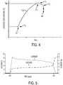
- Fig. 4 is a time-temperature graph depicting changes to localized temperature T LR that illustrate an exemplary thermal pulse generated by self-limiting resistive element 140 during the exemplary disaggregation event described above with reference to Figs. 3(A) to 3(F)
- Fig. 5 is a time-voltage/current graph illustrating exemplary operating characteristics of self-limiting resistive element 140 during the exemplary disaggregation event.
- localized temperature T LR remains at initial temperature T 0 (e.g., approximately 140°C) until time t11 (i.e., when the flow of trigger current is initiated as described above with reference to Fig. 3(B) ).
- Self-limiting resistive element 140 is configured such that the peak (highest) value of localized temperature T LR (i.e., high/first temperature T 1 , which in the depicted example of Fig. 4 is approximately 220°C), which occurs at time t13, and is above the melting point temperature TMP of the glass forming frangible glass substrate 110.
- T LR peak (highest) value of localized temperature T LR
- T 1 high/first temperature
- TMP melting point temperature
- the current through self-limiting resistive element 140 jumps to a maximum value (e.g., approximately 5 Amps) at time t10, when switch 150 actuates, slowly decreases as resistive portion 142 gradually heats up, and then drops to zero at time t14 when current control element 145 actuates.
- the voltage across self-limiting resistive element 140 gradually increases from 0V at time t10 to an intermediate value (e.g., approximately 4 Volts) as resistive portion 142 gradually heats up, and then jumps to a maximum value (e.g., approximately 9 Volts) at time t14 when current control element 145 actuates.
- Fig. 6 is a perspective view showing a portion of a transient electronic device 100A having a self-limiting resistive element 140A comprising a fuse-type current-limiting portion 145A connected in series between two (first and second) resistor structures (resistive portions) 142A-1 and 142A-2, which are respectively connected to opposing (first and second) terminals 142A-1/2 and disposed over localized region 110-21 in the manner described above.
- terminal 141A-1 is coupled by way of a switch element (not shown) to the direct current (DC) power source and terminal 141A-2 is connected to a suitable ground structure.
- resistor structures 142A-1 and 142A-2 and fuse-type current-limiting portion 145A are produced by depositing a single (common) resistive material (e.g., one or more of magnesium, copper, tungsten, aluminum, molybdenum and chrome) directly onto upper surface 111A of frangible glass substrate 110A.
- a single resistive material e.g., one or more of magnesium, copper, tungsten, aluminum, molybdenum and chrome
- the critical issue associated with the selection of the resistive material is that it is sufficiently conductive and adheres to upper surface 111A of frangible glass substrate 110A well enough that heat generated by resistive portions 142A-1 and 142A-2 and current-limiting portion 145A is transferred efficiently into localized region 110-21 during the rapid heating process of a thermal pulse.
- resistive material is printed, etched or otherwise patterned such that resistor structures 142A-1 and 142A-2 respectively comprise relatively large structures 142A-1/2, and fuse-type current-limiting portion 145A comprises a relatively narrow thin structure configured to function as a fuse element. That is, when a sufficiently large current passes between terminals 141A-1 and 141A-2, resistor structures 142A-1 and 142A-2 and current-limiting portion 145A undergo resistive heating, but its relatively narrow cross-section causes current-limiting portion 145A to produce a higher temperature, which in the preferred embodiment is sufficient to cause melting and breakage when subjected to a suitable trigger current.
- Figs. 7(A) and 7(B) are top plan views showing self-limiting resistive elements 140B-1 and 140B-2 including bowtie-type patterned metal layer structure disposed directly on upper surface 111B of frangible glass substrate 110B, with each resistive element including a fuse element connected between downward-tapered sections of two resistor structures.
- self-limiting resistive element 140B-1 includes a first resistor structure 142B-11 including a downward-tapered section 146B-11, a second resistor structure 142B-12 including a downward-tapered section 146B-12, and a fuse element 145B-1 connected between tapered ends 147B-11 and 147B-12 of downward-tapered sections 146B-11 and 146B-12, respectively.
- self-limiting resistive element 140B-2 includes a first resistor structure 142B-21 including a downward-tapered section 146B-21, a second resistor structure 142B-22 including a downward-tapered section 146B-22, and a fuse element 145B-2 connected between tapered ends 147B-21 and 147B-22.
- fuse elements 145B-1 and 145B-2 comprise narrow neck structures having widths W1 that are configured to melt and break when subjected to a trigger current.
- width W1 is greater than a thickness frangible glass substrate 110B (e.g., thickness T shown in Fig. 6 ).
- fuse elements 145B-1 and 145B-2 have widths W1 of at least 0.3 mm.
- the resistor structures of both self-limiting resistive elements e.g., resistor structure 146B-11
- resistor structure 146B-11 can have almost any width (size) W2, although larger resistors require more power and energy from the power source.
- fuse element 145B-1 comprises a straight rectangular structure extending between tapered ends 147B-11 and 147B-12
- fuse element 145B-2 comprises an S-shaped structure extending between tapered ends 147B-21 and 147B-22.
- Fig. 8 is a circuit diagram showing a partial transient electronic device 100C including a remotely (wirelessly) controllable trigger mechanism 130C including a sensor 160C configured to detect a transmitted wave signal WS (e.g., a light wave signal, a radio frequency (RF), or an acoustic/sound signal), and configured to then generate the electronic trigger signal TS used to actuate the switch element.
- a transmitted wave signal WS e.g., a light wave signal, a radio frequency (RF), or an acoustic/sound signal
- trigger mechanism 130C includes a self-limiting resistive element 140C and a switch element 150C, where self-limiting resistive element 140C includes a fuse element 145C connected between a first resistor structure 142C-1 and a second resistor structure 142C-2.
- switch element 150C is implemented using a silicon controlled rectifier
- wave signal WS is an optical signal
- sensor 160C is a photodiode (or other light wave sensor) operably coupled to switch element 150C and configured to activate in response to optical signal WS such that current through photodiode 160C actuates switch element 150C by way of utilizing the current to cause the silicon controlled rectifier to latch, which in turn couples battery PS across self-limiting resistor element 140C, ultimately causing disaggregation (fragmentation) of the glass substrate and any included electronics in the manner described above.
- RF signals and acoustic wave signals may be utilized by replacing photodiode 160C with a radio-frequency wave sensor or an acoustic wave sensor.
- other physical and chemical stimuli may also be utilized in conjunction with an appropriate sensor to initiate a fragmentation sequence.
- latching is achieved using silicon controlled rectifier 150C in the practical embodiment, other switch elements may also be utilized, such as a latch circuit comprising a single MOSFET transistor or a MOSFET-based multiple-element circuit.
- Figs. 9(A) and 9(B) show simplified transient electronic devices 100D-1 and 100D-2 according to alternative practical embodiments in which sensor and/or switch elements are either fabricated or mounted directly on the "host" frangible glass substrate, or fabricated concurrently with the electronic elements on a semiconductor layer.
- Fig. 9(A) shows a device 110D-1 in which a sensor 160D-1 (e.g., a photodiode) and a switch element 150D-1 (e.g., a silicon controlled rectifier) are implemented by suitable materials printed or patterned directly onto surface 111D of frangible glass substrate 110D.
- a sensor 160D-1 e.g., a photodiode
- a switch element 150D-1 e.g., a silicon controlled rectifier
- device 110D-2 includes a sensor 160D-2 and a switch element 150D-2 fabricated using CMOS fabrication techniques on a semiconductor structure 121D-2 (e.g., IC chip or SOI layer) on which the electronic elements 122D are formed.
- CMOS fabrication techniques e.g., CMOS fabrication techniques
- a semiconductor structure 121D-2 e.g., IC chip or SOI layer
- self-limiting resistive elements 140D-1 and 140D-2 are formed directly on substrates 1
- one or both of the sensor and switch element may be disposed on a host PC board and connected by way of suitable conductive connection to the
Landscapes
- Engineering & Computer Science (AREA)
- Physics & Mathematics (AREA)
- Mathematical Physics (AREA)
- Computer Security & Cryptography (AREA)
- Computer Hardware Design (AREA)
- Computing Systems (AREA)
- General Engineering & Computer Science (AREA)
- Fuses (AREA)
- Semiconductor Integrated Circuits (AREA)
- Logic Circuits (AREA)
- Structure Of Printed Boards (AREA)
Abstract
Description
- This invention relates to transient electronics, and in particular to trigger devices and triggering methods utilized to initiate the fragmentation of frangible glass substrates in transient electronic assemblies.
- Large area sensing is critical for a variety of military, ecological and commercial interests and has historically been served through the use of centralized long-range sensors. However, rapid improvements in miniaturization of electronic systems have significantly improved the capabilities of small sensor devices. These micro-sensors have the potential to create "large N" distributed networks with advantages in operational adaptability, non-traditional sensing modalities that are only possible with close proximity, increased sensitivity and knowledge extraction through networked intelligence.
- While distributed network systems have remarkable promise, their realistic use is limited by risks associated with their accumulation in the environment, detection and defeat, and exploitation due to inability to maintain positive control (unlike centralized long-range sensors).
- The phrase "transient electronics" refers to a relatively new family of electronic devices that disappear (disaggregate and disperse) within a set period of time, making them ideally suited for distributed network systems. Conventional transient electronic systems typically rely on the use of soluble substrates and electronic materials (such as silk). When placed into solvent (typically water), these conventional substrates and electronics slowly dissolve into solution. As such, a distributed network system made up of conventional transient electronic devices can be expected to "disappear" over a relatively short amount of time (e.g., after periodic rainfall).
- Although the conventional transient electronic approaches achieve the goal of causing the electronics to "disappear" after use, the long dissolution period required to achieve complete disaggregation and dispersal make the conventional approaches unfit for discrete (e.g., military) applications that require rapid and complete disaggregation upon command. Moreover, early conventional approaches utilize materials that were not compatible with existing integrated circuit fabrication and assembly techniques, requiring the development of new IC fabrication processes at significant cost.
- More recently, a new type of transient electronic device was introduced in which functional circuitry fabricated using well-known low-cost fabrication techniques (e.g., CMOS or SOI) and disposed on a frangible glass substrate that, when subjected to a small initial fracture force, underwent complete disaggregation (shattering) in a manner that releases sufficient potential energy to also cause disaggregation of the functional circuitry. The transient event (i.e., disaggregation) was controlled by a trigger mechanism configured to generate the required initial fracture force by way of applying resistive heating, a chemical reaction or a localized mechanical pressure to the frangible glass substrate in response to a suitable trigger signal. An issue with some triggering approaches is that they may require a substantial electronic system to provide a particular current or voltage pulse in order to provide the necessary conditions to initiate fragmentation. For example, resistive heating type trigger mechanisms may require a pulse shaping circuit configured to generate and transmit a shaped current pulse from a power source to the resistive heating element in order to generate initial fracture.
- What is needed is a simple and reliable trigger mechanism and triggering method for initiating the powderization of a frangible glass substrate in a transient electronic device that reliably achieves complete, on-command disaggregation of the electronic circuitry formed thereon in response to an electronic trigger signal.
- The present invention is directed to a simple and reliable trigger mechanism and associated triggering method for reliably initiating powerderization of functional circuitry (electronic elements) in a transient electronic device by way of generating a localized thermal pulse (i.e., rapid heating followed by rapid cooling) using a self-limiting circuit arrangement that avoids the need for current pulse shaping circuitry and/or complicated connection arrangements, thereby avoiding the problems associated with conventional approaches.
- According to an aspect of the invention, the trigger mechanism includes a self-limiting resistive element that is at least partially formed on a frangible glass substrate. The frangible glass substrate is constructed substantially entirely from a glass material having an associated melting point temperature using known techniques such that it undergoes complete disaggregation (shattering) in response to an applied initial fracture force. The electronic elements (e.g., a silicon-on-insulator-based (SOI-based) IC, a chip-based IC, or thin-film electronics patterned directly onto the frangible glass substrate) and the self-limiting resistive element of the trigger mechanism are fixedly attached to one or both surfaces of the frangible glass substrate, with the electronic elements typically dispose over a first region of the frangible glass substrate, and the self-limiting resistive element disposed over a localized (i.e., relatively small) second region of the frangible glass substrate. With this arrangement, the localized thermal pulse generated by the self-limiting resistive element produces a stress profile caused by rapid heating above the glass' melting point temperature and then cooling in the localized region located adjacent (e.g., below) the self-limiting resistive element. By configuring the trigger mechanism in the manner described below, the resulting stress profile generates the desired initial fracture force in the localized region, thereby initiating the complete disaggregation of the frangible glass substrate, along with the electronic elements disposed thereon.
- According to another aspect of the present invention, the self-limiting resistive element includes a current-limiting portion (e.g., a fuse, timer-based or thermistor-based circuit) that independently controls (i.e., without requiring an externally-generated control signal) an amount generated heat by way of terminating the flow of a trigger current through the self-limiting resistive element after a predetermined amount of generated heat is transmitted into the localized region of the frangible glass substrate. In an exemplary embodiment, the current-limiting portion is implemented by a fuse structure that is configured to melt/break after a predetermined amount of heat is generated by the self-limiting resistive element, thereby producing an open circuit that terminates further heat generation by way of preventing further trigger current flow through the self-limiting resistive element. Moreover, by configuring the self-limiting resistive element in the manner described below such that heat rapidly dissipates from the localized region of the frangible glass substrate after termination of the trigger current, the self-limiting resistive element provides a simple and reliable mechanism for generating the desired thermal pulse and resulting stress profile that produce the initial fracture force in the localized region of the frangible glass substrate.
- According to another aspect of the present invention, the self-limiting resistive element facilitates electronic control of the triggering event using very simple addressing electronics, thereby minimizing system complexity. That is, because the self-limiting resistive element eliminates the need for current shaping electronics, the trigger mechanism is able to achieve complete, on-command disaggregation of the electronic circuitry formed on the frangible glass substrate using a simple switch element that is controllable (i.e., actuated to generate the trigger current) by way of an electronic trigger signal to selectively couple the self-limiting resistive element to a direct-current (DC) power source (e.g., a battery). Using this arrangement, the switch element is turned on at the beginning of a transient event in response to the electronic trigger signal, thereby initiating a large direct current (i.e., the trigger current) to flow from the DC power source through the self-limiting resistive element, whereby the self-limiting resistive element operates as described above to generate the thermal pulse resulting in the initial fracture force causing disaggregation of the frangible glass substrate. As such, in contrast to conventional resistive-heat-type trigger mechanisms that require pulse shaping circuity and complicated addressing arrangements, the triggering mechanism of the present invention is simple and reliable, thereby reducing manufacturing costs and complexity.
- As mentioned above, characteristics of the thermal pulse (i.e., the rate and duration of heat generation that produces the rapid temperature increase) are entirely independently controlled by operation of the self-limiting resistive element (i.e., without requiring an externally-generated control signal). Specifically, the self-limiting resistive element is configured to generate resistive heat (i.e., by way of passing the large trigger current through one or more resistor structures) for a predetermined amount of time after actuation of the switch element, whereby a temperature of the localized region of the frangible glass substrate rapidly increases from a relatively low initial temperature (e.g., approximately 140°C) to a high (first) temperature level temperature (e.g., approximately 220°C) that is above the melting point temperature of the glass forming the frangible glass substrate. The self-limiting resistive element is further configured to independently control the amount of generated heat by way of terminating the flow of trigger current through the resistor element(s) at the end of the predetermined time period, whereby terminating the heat generating process causes rapid cooling of the localized region (e.g., from the high (first) temperature (e.g., 220°C) to a lower (second) temperature (e.g., approximately 200°C), e.g., in approximately one second) by way of heat dissipation from the localized region into surrounding substrate regions. The present inventors determined that a thermal pulse generated in this manner produces a stress profile that reliably generates an initial fracture force in the localized region having sufficient strength to produce subsequent propagating fracture forces that pass throughout the frangible glass substrate, causing "powderization" (i.e., disaggregation or fragmentation) of the frangible glass substrate into micron-sized particulates. When a transient electronic device is constructed in accordance with the present invention, sufficient potential energy is released from the disaggregating/fragmenting glass substrate to cause propagation of cracks from the glass substrate into the electronic elements and other device structures (e.g., the self-limiting resistive element) with sufficient force to entirely powderize these structures as well. Because the trigger mechanism produces the rapid heating/cooling stress profile using only a simple switch and a self-limiting resistive element (i.e., without requiring an external control signal or other circuitry capable of generating a shaped current pulse), the present invention provides a low-cost and reliable triggering mechanism for initiating powderization of electronic elements disposed on a transient electronic device.
- According to an embodiment of the present invention, the self-limiting resistive element is entirely formed by a resistive material that is deposited and patterned directly onto a surface of the frangible glass substrate using a standard thin-film fabrication technique (e.g., photolithographic or inkjet printing). In alternative embodiments, the resistive material includes magnesium, copper, tungsten, aluminum, molybdenum or chrome, or a combination of one or more of these metals. Other suitable materials may also be used, provided the material is sufficiently conductive and adheres to the frangible glass substrate surface well enough that heat is transferred efficiently into the localized region during the rapid heating portion of the thermal pulse.
- According to an embodiment of the present invention, the self-limiting resistive element includes one or more resistive portion connected in series with the current-limiting portion between two (first and second) terminals, with the first terminal is coupled by way of the switch element to the direct current (DC) power source and the second terminal connected to a suitable ground structure. In one embodiment, the resistive material mentioned above is patterned to form two relatively large resistor structures connected by a narrow fuse element, where the resistor structures are configured to heat up but remain coherent during the thermal pulse, and the fuse element is configured to melt and break at the end of the rapid heating (first) time period. The use of a fuse element to implement the current-control portion of the self-limiting resistive element provides a low-cost, simple and highly reliable structure for independently controlling the amount of heat generated during the rapid heating process, and reliably produces an open circuit condition (i.e., by way of melting/breaking) that terminates flow of the trigger current through the resistor structures at the start of the rapid cooling portion of the thermal pulse.
- In a presently preferred embodiment, the resistive material utilized to form the self-limiting resistive element is patterned into a bowtie-type structure in which the two resistor structures including respective downward-tapered sections, and the fuse element is formed by a narrow section of resistive material connected between tapered ends of the downward-tapered sections. In one embodiment, the fuse element includes a straight rectangular structure extending between the tapered end, and in another embodiment the narrow resistive material section forming the fuse element is disposed in a substantially S-shaped pattern. In either case, a width W of the narrow resistive material section is greater than a thickness of the frangible glass substrate determines to induce reliable disaggregation. In a practical embodiment using a 0.25 mm thick frangible glass substrate, the narrow resistive material section forming the fuse element has a width of at least 0.3 mm. In contrast, resistor structures can have almost any size, although while larger resistors ensure reliable fragmentation, they also require more power and energy from the power source. Accordingly, the smallest possible resistor structures are preferred in order to minimize power and energy requirements.
- According to an embodiment of the present invention, to facilitate remote (wireless) control over the transient electronic device, the transient electronic device further includes a sensor configured to detect a transmitted wave signal (e.g., a light wave signal, a radio frequency (RF), or an acoustic/sound signal), and configured to then generate the electronic trigger signal used to actuate the switch element. In an exemplary embodiment, a remote optical signal is detected by a photodiode (light wave sensor), whereby current through the photodiode causes a silicon controlled rectifier (switch element) to latch, which in turn couples a battery across the self-limiting resistor element, ultimately causing disaggregation (fragmentation) of the glass substrate and any included electronics. While remote actuation of the transient electronic device is achieved using an optical signal in this example, RF signals and acoustic wave signals may be utilized by replacing the photodiode with a radio-frequency wave sensor or an acoustic wave sensor. Moreover, other physical and chemical stimuli may also be utilized in conjunction with an appropriate sensor to initiate a fragmentation sequence. Similarly, while latching is achieved using a silicon controlled rectifier, other switch elements may also be utilized, such as a single MOSFET transistor or a multiple-element latch circuit.
- According to other alternative practical embodiments, one or more of the switch element and sensor utilized to control operation of the triggering mechanism may be formed/mounted directly on the frangible glass substrate, formed on a semiconductor layer/die on which the electronic elements are formed, or disposed on an external printed circuit board to which the transient electronic device is attached. For example, in the practical embodiment described above, one or both of the photodiode/sensor and the silicon controlled rectifier (switch) may be implemented by patterning suitable materials directly onto the frangible glass substrate, or may be implemented using CMOS fabrication techniques on a semiconductor structure (e.g., IC chip or SOI layer) on which the electronic elements are formed and that is fixedly attached to the frangible glass substrate.
- In additional alternative embodiments, the frangible glass substrate comprises one of a stressed glass substrate including stress-engineered tensile and compressive layers that are operably attached together, a thermally tempered glass substrate including laminated layers of different glass types having associated different coefficient of thermal expansion (CTE) values, and an ion-exchange treated glass substrate. In each case, the frangible glass substrate contains enough stored energy to generate self-propagating secondary fractures in response to an initial fracture force such that the glass substrate completely disaggregates ("powderizes") into micron-sized particulates by way of a mechanism similar to that captured in a Prince Rupert's Drop. In alternative embodiments, the electronic devices are either fabricated directly onto the frangible glass substrate using standard silicon-on-insulator (SOI) fabrication techniques (i.e., such that the functional circuitry is implemented as an SOI integrated circuit structure), or are separately fabricated on an IC die (chip) that is then attached to the frangible glass substrate using anodic bonding. In either case, the released potential energy during disaggregation of the frangible glass substrate is sufficient to also powderize the electronic devices, along with the trigger mechanism and any other structures that might be disposed on the frangible glass substrate.
- These and other features, aspects and advantages of the present invention will become better understood with regard to the following description, appended claims, and accompanying drawings, where:
-
Fig. 1 is a top side perspective view showing a transient electronic device including a trigger mechanism disposed on a frangible glass substrate according to a simplified embodiment of the present invention; -
Fig. 2 is a flow diagram showing a generalized method for triggering a disaggregation event on the transient electronic device depicted inFig. 1 ; -
Figs. 3(A), 3(B), 3(C), 3(D), 3(E) and 3(F) are partial cross-sectional side views showing a portion of the transient electronic device ofFig. 1 at various moments during a disaggregation event; -
Fig. 4 is a time-temperature graph illustrating an exemplary thermal pulse generated during the disaggregation event described with reference toFigs. 3(A) to 3(F) ; -
Fig. 5 is a time-voltage/current graph illustrating exemplary operating characteristics of a trigger mechanism utilized during the disaggregation event described with reference toFigs. 3(A) to 3(F) ; -
Fig. 6 is a partial perspective view showing the self-limiting resistive element of a triggering mechanism according to an exemplary practical embodiment of the present invention; -
Figs. 7(A) and7(B) are top plan views showing self-limiting resistive elements having bowtie-type patterns according to alternative exemplary specific embodiments of the present invention; -
Fig. 8 is a circuit diagram showing an exemplary trigger mechanism configured for remote actuation according to another embodiment of the present invention; and -
Figs. 9(A) and 9(B) are simplified perspective views showing transient electronic devices including remote actuation according to alternative specific embodiments. - The present invention relates to an improvement in transient electronic devices. The following description is presented to enable one of ordinary skill in the art to make and use the invention as provided in the context of a particular application and its requirements. As used herein, directional terms such as "upper", "upward", "lower", "downward" and "over" are intended to provide relative positions for purposes of description, and are not intended to designate an absolute frame of reference. The terms "coupled" and "connected", which are utilized herein, are defined as follows. The term "connected" is used to describe a direct connection between two circuit elements, for example, by way of a metal line formed in accordance with normal integrated circuit fabrication techniques. In contrast, the term "coupled" is used to describe either a direct connection or an indirect connection between two circuit elements. For example, two coupled elements may be directly connected by way of a metal line, or indirectly connected by way of an intervening circuit element (e.g., a capacitor, resistor, inductor, or by way of the source/drain terminals of a transistor). Various modifications to the preferred embodiment will be apparent to those with skill in the art, and the general principles defined herein may be applied to other embodiments. Therefore, the present invention is not intended to be limited to the particular embodiments shown and described, but is to be accorded the widest scope consistent with the principles and novel features herein disclosed.
-
Fig. 1 includes simplified perspective views showing a transientelectronic device 100 in a pre-transience "whole" state (i.e., device 100(t0) shown in the middle portion ofFig. 1 ) and a post-transience "powderized" state (i.e., device 100(t2) shown in the lower portion ofFig. 1 ). In the pre-transience state (e.g., immediately after production, during normal operation, and during portions of the transient event occurring prior to disaggregation), transient electronic device 100(t0) generally includesfunctional electronics 120 and atrigger mechanism 130 that are disposed over corresponding regions offrangible glass substrate 110. In the preferred embodiment depicted by device 100(t2) at the bottom ofFig. 1 , in the post-transience "powerderized" state, the frangible glass substrate and any structures disposed thereon (i.e.,functional electronics 120 and any portion oftrigger mechanism 130 mounted on frangible glass substrate 110) are completely disaggregated ("powderized") into micron-sized particulates 101 (i.e., have sizes ≤ 100 µm across). - In order to produce transient
electronic device 100 such that it achieves the preferred post-transience "powerderized" state depicted inFig. 1 , it is necessary to manufacture or procure frangible glass substrates having the characteristics set forth below. Referring to the middle ofFig. 1 ,frangible glass substrate 110 is a wafer-like structure having opposing upper andlower surfaces trigger mechanism 130. In one specific embodiment,frangible glass substrate 110 includes at least one glass structure including a first glass material having a first coefficient of thermal expansion (CTE) value, and multiple second glass structures respectively including one or more different (second) glass materials respectively having a second CTE value, where the second CTE value is different from the first CTE value. For example, as indicated in the upper right bubble inFig. 1 , thermally temperedglass substrate 110A includes aglass structure 110A-1 disposed between twoglass structures 110A-21 and 110A-22, whereglass structure 110A-1 comprises a different glass material having a different CTE value than the glass material from whichglass structures 110A-21 and 110A-22 are formed. Similarly, as indicated in the upper left bubble ofFig. 1 , thermally temperedglass substrate 110B includes (second)glass structures 110B-21, 110B-22 and 110B-23 disposed in a (first)glass structure 110B-1, whereglass structure 110B-1 comprises a different glass material than that ofglass structures 110B-21 to 110B-23. The fabrication of such thermally tempered glass substrates is described inU.S. Pub. App. No. 2015/0358021-A1 , which is incorporated herein by reference in its entirety. In another alternative specific embodiment,frangible glass substrate 110 comprises a stressed glass substrate including stress-engineered tensile and compressive layers that are operably attached together in the manner described inU.S. Patent No. 9,154,138 frangible glass substrate 110 an ion-exchange treated glass substrate or interposer fabricated in the manner described inU.S. Pat. App. Ser. No. 14/694,132 frangible glass substrate 110 contains enough stored energy to generate self-propagating secondary fractures in response to an initial fracture force such that, as depicted by device 100(t2) at the bottom ofFig. 1 ),frangible glass substrate 110 completely disaggregates ("powderizes") into micron-sized particulates (i.e., ≤ 100 µm across) using a mechanism similar to that captured in a Prince Rupert's Drop. In addition, the released potential energy during disaggregation offrangible glass substrate 110 is sufficient to also powderizefunctional electronics 120 as also illustrated by device 100(t2). In one embodiment, the released potential energy also powderizes portions oftrigger mechanism 130 and any other structures that might be disposed onfrangible glass substrate 110. -
Functional electronics 120 includeelectronic elements 122 fabricated on a semiconductor base layer 121 (e.g., an SOI layer or an integrated circuit (IC) die/chip) that is fixedly attached toupper surface 111 and dispose over a corresponding region 110-1 offrangible glass substrate 110. As set forth above, the main purpose of transient electronics is to provide a way to essentially entirely eliminate an IC or other electronic elements for purposes of protecting the environment or maintaining confidentiality (i.e., preventing unauthorized reverse engineering of the elements/circuit). A benefit of fabricating transientelectronic device 100 onfrangible glass substrate 110 is that this approach both facilitates formingfunctional electronics 120 using low cost manufacturing techniques, and facilitates reliable elimination offunctional electronics 120 by way of causing disaggregation offrangible glass substrate 110. In a preferred embodiment,functional electronics 120 are fabricated by way of formingelectronic elements 122 on a suitable semiconductor (base)layer 121 using existing IC fabrication techniques (e.g., CMOS), andelectronic elements 122 are configured to perform a prescribed useful function (e.g., sensor operations) up until the transient event. In one embodiment, thesemiconductor layer 121 is a silicon "chip" (die) upon whichelectronic elements 122 are fabricated, and then thesemiconductor layer 121 is fixedly attached toglass substrate 110 using known die bonding techniques (e.g., anodic bonding or by way of sealing glass) that assure coincident powderization ofelectronic elements 122 withfrangible glass substrate 110. In a presently preferred embodiment,functional electronics 120 includeselectronic elements 122 configured to form an IC device using standard silicon-on-insulator (SOI) fabrication techniques (i.e., such that the functional circuitry is implemented as an SOI integrated circuit structure). In another embodiment,functional electronics 120 are fabricated on an IC die that is "thinned" (e.g., subjected to chemical mechanical polishing) before the bonding process. - As set forth above,
trigger mechanism 130 is configured to generate an initial fracture force infrangible glass substrate 110 in response to an electronic trigger signal TS. According to the present invention,trigger mechanism 130 achieves this function using a self-limitingresistive element 140 and aswitch element 150 that are connected in series between a battery (or other DC power source PS) and ground. As depicted inFig. 1 , at least a portion oftrigger mechanism 130 is disposed onupper surface 111 over a second region 110-2 of frangible glass substrate 110 (i.e., away from functional circuitry 120), but may alternatively be formed onlower surface 112.Switch element 150 has a first terminal connected to battery PS, a second terminal connected to a first terminal 141-1 ofelement 140, and a control terminal operably disposed to receive electronic trigger signal TS, which may be generated by an optional sensor or other control circuitry (not shown). As set forth below,switch element 150 is actuated (switched from an open/nonconducting state to a closed/conducing state) at the start of a transient event by way of asserting trigger signal TS, wherebyswitch element 150 initiates a DC trigger current IT that flows from battery PS through self-limitingresistive element 140 to ground. In one embodiment, self-limitingresistive element 140 includes aresistive portion 142 and a current-limitingportion 145 that are connected in series between battery PS and ground by way of a first terminal 141-1 and a second terminal 141-2, respectively, where at least one ofresistive portion 142 and a current-limitingportion 145 are disposed onupper surface 111 over a localized (i.e., relatively small) region 111-21 offrangible glass substrate 110. One or both ofresistive portion 142 and a current-limitingportion 145 are configured and operably thermally coupled tofrangible glass substrate 110 such that self-limitingresistive element 140 generates heat at a rate that rapidly increases a localized temperature of localized region 110-21, and current limitingportion 145 is further configured to independently control (i.e., without requiring an externally-generated control signal) the flow of trigger current IT by way of terminating the flow of trigger current IT after localized region 110-21 receives a sufficiently large amount of the heat generated by self-limitingresistive element 140. In a preferred embodiment described below, current-limitingportion 145 is implemented by a fuse element configured to fail (melt and break) after conducting a predetermined amount of trigger current IT (i.e., after a predetermined amount of heat is generated by self-limiting resistive element 140). In other embodiments, current-limitingportion 145 may be implemented by other elements/circuits configured to implement the described independent control over trigger current IT, such as a thermistor-based circuit configured to terminate the trigger current flow upon detecting a predetermined temperature level, or a timer-based circuit configured to terminate the trigger current flow a preset time after actuation ofswitch element 150. -
Fig. 2 is a flow diagram showing a generalized method for triggering a disaggregation event on transient electronic device 100 (shown inFig. 1 ), andFigs. 3(A), 3(B), 3(C), 3(D), 3(E) and 3(F) are partial cross-sectional side views showing a portion of transientelectronic device 100 before and during an exemplary disaggregation event. - Referring to the top of
Fig. 2 , transient electronic device 100(t0) (Fig. 1 ) is subjected to normal operation (i.e.,functional circuitry 120 performs as intended).Fig. 3(A) is a simplified cross-section showing a portion of device 100(t0), whereresistive portion 142 of self-limitingresistive element 140 is depicted as a metal structure disposed onupper surface 111 of thefrangible glass substrate 110 over localized region 110-21, andcurrent control portion 145 is depicted as a switch in a closed (i.e., conducting) state. At this time t0,switch portion 150 is open (i.e., in a nonconducting state), so no current passes from battery PS through self-limitingresistive element 140, and thus no heat is generated byresistive portion 142. Accordingly, at time t0, a localized temperature TLR in localized region 110-21 assumes the same (relatively low) initial temperature To as that of surrounding adjacent regions 100-22 offrangible glass substrate 110. - Referring to block 205 near the top of
Fig. 2 , the transient event is initiated at a time t10, for example, when a trigger event signal is detected by a sensor (e.g., in response to a wirelessly transmitted light or RF signal), or unauthorized tampering is detected. - As indicated in block 210 (
Fig. 2 ) andFig. 3(B) , at a time t11 (i.e., a moment after time t10), trigger signal TS (Fig. 1 ) is asserted and applied to the control terminal ofswitch element 150, wherebyswitch 150 is actuated to initiate the flow of trigger current IT throughresistive portion 142 andcurrent control portion 145 to ground, wherebyresistive portion 142 begins to generate heat HG that is transmitted throughupper surface 111 offrangible glass substrate 110 into localized region 110-21, thereby causing localized temperature TLR to increase above initial temperature To. - As indicated in block 220 (
Fig. 2 ) andFig. 3(C) , at a subsequent time t12, the continued flow of trigger current IT causesresistive portion 142 to generate heat HG at a rate that rapidly increases localized temperature TLR toward a predetermined target temperature T1. According to an aspect of the invention, this rapid temperature increase occurs at a rate that causes localized temperature TLR to increase at a rate faster than the temperature in surrounding regions 110-22. That is, as indicated inFig. 3(C) , generated heat HG from self-limitingresistive element 140 enters localized region 110-21 at a faster rate than dissipating heat HG leaves localized region 110-21 into surrounding regions 110-22, thereby causing localized temperature TLR of localized region 110-21 to rapidly increase from the initial temperature To toward the higher target (first) temperature level T1 while surrounding regions 110-22 remain at a substantially lower temperature. - As indicated in block 230 (
Fig. 2 ) andFig. 3(D) , at time t13, current limitingportion 145 actuates to terminate the generation of heat HG by way of generating an open circuit condition that terminates the flow of trigger current throughresistive portion 142. According to another aspect of the invention, self-limiting resistive element is configured such that the termination of generated heat causes a rapid decrease of localized temperature TLR toward a lower (second) temperature T2 by way of heat HD dissipating out of localized region 110-21 into cooler surrounding regions 110-22. - As indicated in block 240 (
Fig. 2 ) andFig. 3(E) , at time t14, the thermal pulse generated by the rapid temperature increase and rapid temperature decrease described above with reference toFigs. 3(C) and 3(D) produces a stress profile in localized region 110-21 offrangible glass substrate 110 that is sufficient to produce an initial fracture force F0 in localized region 110-21. - As indicated in block 240 (
Fig. 2 ) andFig. 3(E) , at time t14, the thermal pulse generated by the rapid temperature increase and rapid temperature decrease described above with reference toFigs. 3(C) and 3(D) produces a stress profile in localized region 110-21 offrangible glass substrate 110 that has sufficient force to produce an initial fracture force F0 in localized region 110-21. Subsequently, as indicated in block 250 (Fig. 2 ) andFig. 3(F) , at time t15, the initial fracture force F0 produces propagating fracture forces FP that radiate from localized region 110-21 throughoutfrangible glass substrate 110 andelectronic elements 122, thereby causing the complete disaggregation depicted by device 100(t2) at the bottom ofFig. 1 . Accordingly, by configuringtrigger mechanism 130 such that it generate the thermal pulse infrangible glass substrate 110 as described above, and by configuringfrangible glass substrate 110 such that it generates initial fracture force F0 in localized region 110-21 in response to the applied thermal pulse, and such that initial fracture force F0 causes propagating fracture forces FP that result in complete disaggregation offrangible glass substrate 110 andelectronic elements 122 in the manner described above, the present invention facilitates the construction of low-cost, highly reliable transientelectronic devices 100 without the need for pulse shaping circuity and complicated addressing arrangements. -
Fig. 4 is a time-temperature graph depicting changes to localized temperature TLR that illustrate an exemplary thermal pulse generated by self-limitingresistive element 140 during the exemplary disaggregation event described above with reference toFigs. 3(A) to 3(F) , andFig. 5 is a time-voltage/current graph illustrating exemplary operating characteristics of self-limitingresistive element 140 during the exemplary disaggregation event. As indicated inFig. 4 , localized temperature TLR remains at initial temperature T0 (e.g., approximately 140°C) until time t11 (i.e., when the flow of trigger current is initiated as described above with reference toFig. 3(B) ). The subsequent rapid increase during the period from time t11 to time t13 is caused by generated heat HG entering localized region 110-21 in the manner described above with reference toFigs. 3(B) and 3(C) . Self-limitingresistive element 140 is configured such that the peak (highest) value of localized temperature TLR (i.e., high/first temperature T1, which in the depicted example ofFig. 4 is approximately 220°C), which occurs at time t13, and is above the melting point temperature TMP of the glass formingfrangible glass substrate 110. After self-limitingresistive element 140 actuates, heat begins dissipating from localized region 110-21 into surrounding regions 110-22 offrangible glass substrate 110, as depicted inFig. 3(D) , causing the subsequent rapid temperature decrease during the period from time t13 to time t14 (e.g., approximately 20°C from approximately 220°C to approximately 200°C in approximately one second in the depicted example shown inFig. 4 ). At time t14, the stress profile caused by the rapid increase to temperature T1 followed by the period of rapid cooling produces initial fracture force F0 in localized region 110-21, as depicted inFig. 3(E) . Almost immediately after time t14, initial fracture force F0 cause propagating fracture forces FP that completelydisaggregate device 100 in a very short amount of time, as depicted inFig. 3(F) , resulting is rapid cooling. As indicated inFig. 5 , the current through self-limitingresistive element 140 jumps to a maximum value (e.g., approximately 5 Amps) at time t10, whenswitch 150 actuates, slowly decreases asresistive portion 142 gradually heats up, and then drops to zero at time t14 whencurrent control element 145 actuates. In contrast, the voltage across self-limitingresistive element 140 gradually increases from 0V at time t10 to an intermediate value (e.g., approximately 4 Volts) asresistive portion 142 gradually heats up, and then jumps to a maximum value (e.g., approximately 9 Volts) at time t14 whencurrent control element 145 actuates. -
Fig. 6 is a perspective view showing a portion of a transientelectronic device 100A having a self-limitingresistive element 140A comprising a fuse-type current-limitingportion 145A connected in series between two (first and second) resistor structures (resistive portions) 142A-1 and 142A-2, which are respectively connected to opposing (first and second)terminals 142A-1/2 and disposed over localized region 110-21 in the manner described above. As in the embodiment shown inFig. 1 , when operably connected together, terminal 141A-1 is coupled by way of a switch element (not shown) to the direct current (DC) power source and terminal 141A-2 is connected to a suitable ground structure. In a preferred embodiment,resistor structures 142A-1 and 142A-2 and fuse-type current-limitingportion 145A are produced by depositing a single (common) resistive material (e.g., one or more of magnesium, copper, tungsten, aluminum, molybdenum and chrome) directly ontoupper surface 111A offrangible glass substrate 110A. The critical issue associated with the selection of the resistive material is that it is sufficiently conductive and adheres toupper surface 111A offrangible glass substrate 110A well enough that heat generated byresistive portions 142A-1 and 142A-2 and current-limitingportion 145A is transferred efficiently into localized region 110-21 during the rapid heating process of a thermal pulse. The resistive material is printed, etched or otherwise patterned such thatresistor structures 142A-1 and 142A-2 respectively comprise relativelylarge structures 142A-1/2, and fuse-type current-limitingportion 145A comprises a relatively narrow thin structure configured to function as a fuse element. That is, when a sufficiently large current passes betweenterminals 141A-1 and 141A-2,resistor structures 142A-1 and 142A-2 and current-limitingportion 145A undergo resistive heating, but its relatively narrow cross-section causes current-limitingportion 145A to produce a higher temperature, which in the preferred embodiment is sufficient to cause melting and breakage when subjected to a suitable trigger current. Implementing current-limitingportion 145A using a fuse-type current-limiting portion (fuse element) provides a low-cost, simple and highly reliable structure for independently controlling the amount of heat generated by self-limitingresistive element 140A during the rapid heating process of a thermal pulse, and reliably produces an open circuit condition (i.e., by way of melting/breaking) that terminates flow of trigger current throughresistor structures 142A-1 and 142A-2 at the start of the rapid cooling portion of the thermal pulse. -
Figs. 7(A) and7(B) are top plan views showing self-limitingresistive elements 140B-1 and 140B-2 including bowtie-type patterned metal layer structure disposed directly onupper surface 111B offrangible glass substrate 110B, with each resistive element including a fuse element connected between downward-tapered sections of two resistor structures. For example, self-limitingresistive element 140B-1 includes afirst resistor structure 142B-11 including a downward-taperedsection 146B-11, asecond resistor structure 142B-12 including a downward-taperedsection 146B-12, and afuse element 145B-1 connected between tapered ends 147B-11 and 147B-12 of downward-taperedsections 146B-11 and 146B-12, respectively. Similarly, self-limitingresistive element 140B-2 includes afirst resistor structure 142B-21 including a downward-taperedsection 146B-21, asecond resistor structure 142B-22 including a downward-taperedsection 146B-22, and afuse element 145B-2 connected between tapered ends 147B-21 and 147B-22. In each case, fuseelements 145B-1 and 145B-2 comprise narrow neck structures having widths W1 that are configured to melt and break when subjected to a trigger current. In a preferred embodiment, width W1 is greater than a thicknessfrangible glass substrate 110B (e.g., thickness T shown inFig. 6 ). For example, in a practical embodiment using a 0.25 mm thick frangible glass substrate, fuseelements 145B-1 and 145B-2 have widths W1 of at least 0.3 mm. In contrast, the resistor structures of both self-limiting resistive elements (e.g.,resistor structure 146B-11) can have almost any width (size) W2, although larger resistors require more power and energy from the power source. - As depicted by the alternative embodiments shown in
Figs. 7(A) and7(B) , different fuse configurations may be utilized to generate desired thermal pulse characteristics. Specifically, self-limitingresistive elements 140B-1 and 140B-2 differ in thatfuse element 145B-1 comprises a straight rectangular structure extending between tapered ends 147B-11 and 147B-12, andfuse element 145B-2 comprises an S-shaped structure extending between tapered ends 147B-21 and 147B-22. These different fuse arrangements provide different benefits, by allowing control over the applied energy and power by tuning the resistance of the trigger as well as tuning the area over which the heat is applied which can impact the time to fragment. -
Fig. 8 is a circuit diagram showing a partial transientelectronic device 100C including a remotely (wirelessly)controllable trigger mechanism 130C including asensor 160C configured to detect a transmitted wave signal WS (e.g., a light wave signal, a radio frequency (RF), or an acoustic/sound signal), and configured to then generate the electronic trigger signal TS used to actuate the switch element. As in the previous embodiment,trigger mechanism 130C includes a self-limitingresistive element 140C and aswitch element 150C, where self-limitingresistive element 140C includes afuse element 145C connected between afirst resistor structure 142C-1 and asecond resistor structure 142C-2. In an exemplary embodiment,switch element 150C is implemented using a silicon controlled rectifier, wave signal WS is an optical signal, andsensor 160C is a photodiode (or other light wave sensor) operably coupled to switchelement 150C and configured to activate in response to optical signal WS such that current throughphotodiode 160C actuatesswitch element 150C by way of utilizing the current to cause the silicon controlled rectifier to latch, which in turn couples battery PS across self-limitingresistor element 140C, ultimately causing disaggregation (fragmentation) of the glass substrate and any included electronics in the manner described above. While remote actuation of the transient electronic device is achieved using an optical signal in this example, RF signals and acoustic wave signals may be utilized by replacingphotodiode 160C with a radio-frequency wave sensor or an acoustic wave sensor. Moreover, other physical and chemical stimuli may also be utilized in conjunction with an appropriate sensor to initiate a fragmentation sequence. Similarly, while latching is achieved using silicon controlledrectifier 150C in the practical embodiment, other switch elements may also be utilized, such as a latch circuit comprising a single MOSFET transistor or a MOSFET-based multiple-element circuit. -
Figs. 9(A) and 9(B) show simplified transientelectronic devices 100D-1 and 100D-2 according to alternative practical embodiments in which sensor and/or switch elements are either fabricated or mounted directly on the "host" frangible glass substrate, or fabricated concurrently with the electronic elements on a semiconductor layer. For example,Fig. 9(A) shows adevice 110D-1 in which asensor 160D-1 (e.g., a photodiode) and aswitch element 150D-1 (e.g., a silicon controlled rectifier) are implemented by suitable materials printed or patterned directly ontosurface 111D offrangible glass substrate 110D. Alternatively, as shown inFig. 9(B) ,device 110D-2 includes asensor 160D-2 and aswitch element 150D-2 fabricated using CMOS fabrication techniques on asemiconductor structure 121D-2 (e.g., IC chip or SOI layer) on which theelectronic elements 122D are formed. In both embodiments, self-limitingresistive elements 140D-1 and 140D-2 are formed directly onsubstrates 1 In another embodiment (not shown), one or both of the sensor and switch element may be disposed on a host PC board and connected by way of suitable conductive connection to the - Although the present invention has been described with respect to certain specific embodiments, it will be clear to those skilled in the art that the inventive features of the present invention are applicable to other embodiments as well, all of which are intended to fall within the scope of the present invention. For example, although self-limiting resistive elements having bowtie-type arrangements are described above, other arrangements may be used.
Claims (10)
- A transient electronic device including:a frangible glass substrate;one or more electronic elements disposed on the frangible glass substrate such that disaggregation of the frangible glass substrate causes disaggregation of the electronic elements; anda trigger mechanism comprising:a self-limiting resistive element consisting of a resistive material disposed over a localized region of said frangible glass substrate; anda switch element coupled to the self-limiting resistive element,wherein said self-limiting resistive element is configured such that:during a first time period after said switch element is actuated to initiate a trigger current from a power source through said self-limiting resistive element, heat generated by said self-limiting resistive element rapidly increases a localized temperature of said localized region from an initial temperature toward a first temperature level, anda current limiting portion of said self-limiting resistive element independently controls the flow of said trigger current such that said trigger current flow is terminated when said localized temperature of said localized region reaches said first temperature level, thereby causing said localized temperature to rapidly decrease from said first temperature level to a second temperature level,wherein said frangible glass substrate is configured such that a stress profile generated in said localized region by a thermal pulse comprising said rapid thermal increase and said rapid thermal decrease is sufficient to produce an initial fracture force in said localized region.
- The transient electronic device according to Claim 1, wherein said resistive material of said self-limiting resistive element comprises one or more of magnesium, copper, tungsten, aluminum, molybdenum and chrome that is disposed directly onto a surface of said frangible glass substrate.
- The transient electronic device according to Claim 1,
wherein said self-limiting resistive element comprises at least one resistive portion connected in series with said current-limiting portion between first and second terminals,
wherein said first terminal is coupled by way of said switch element to a direct current (DC) power source, and
wherein said second terminal is connected to ground. - The transient electronic device according to Claim 3,
wherein said at least one resistive portion comprises first and second resistor structures, and
wherein said current-limiting portion comprises a fuse element connected between said first and second resistor structures and configured to break after said first time period, thereby terminating flow of said said trigger current through said first and second resistor structures. - A triggering method for initiating powderization of electronic elements disposed on a frangible glass substrate consisting essentially of glass having a melting point temperature, said method comprising:generating a rapid thermal increase in a localized region of said frangible glass substrate by actuating a switch element coupled between a power source and a self-limiting resistive element such that a direct current flows from the power source through the switch element and the self-limiting resistive element, thereby causing the self-limiting resistive element to generate and transmit heat into said localized region at a sufficiently high rate to cause a localized temperature of said localized region to rapidly increase from an initial temperature to a first temperature, said first temperature being higher than said melting point temperature; andgenerating a rapid thermal decrease such that said localized temperature in said localized region rapidly decreases from said first temperature to a second temperature, said second temperature being lower than said first temperature, wherein a thermal pulse generated by said rapid thermal increase and said rapid thermal decrease generates an initial fracture force in the localized region,wherein a duration of said rapid thermal increase is independently controlled by said self-limiting resistive element.
- The method of Claim 5, further comprising detecting a wave signal, and wherein generating said rapid thermal comprises controlling said switch element in response to said detected wave signal.
- The method of Claim 6, wherein detecting said wave signal comprises detecting one of a light wave signal, a radio-frequency wave signal, and an acoustic wave signal.
- The method of Claim 6, wherein detecting said wave signal comprises utilizing a photodiode to detect a light signal, and wherein controlling said switch element comprises controlling a silicon controlled rectifier using a current passing through said photodiode.
- A transient electronic device including:a frangible glass substrate;one or more electronic elements disposed on the frangible glass substrate; anda trigger mechanism comprising:a self-limiting resistive element including a fuse element disposed between a first resistor structure and a second resistor structure disposed on said frangible glass substrate; anda switch element coupled between the self-limiting resistive element and a power source such that actuation of said switch element initiates a trigger current from said power source through said self-limiting resistive element,wherein said self-limiting resistive element is configured such that passing said trigger current from said power source through said self-limiting resistive element produces a thermal pulse in said frangible glass substrate, andwherein said frangible glass substrate is configured such that a stress profile generated by said thermal pulse causes an initial fracture force in said localized region, and said frangible glass substrate is further configured such that said initial fracture force causes propagating fracture forces that result in complete disaggregation of said frangible glass substrate and said one or more electronic elements.
- The transient electronic device according to Claim 9, wherein said switch element comprises one of a silicon controlled rectifier, a single transistor and a multiple-element circuit.
Applications Claiming Priority (1)
| Application Number | Priority Date | Filing Date | Title |
|---|---|---|---|
| US15/220,164 US10026579B2 (en) | 2016-07-26 | 2016-07-26 | Self-limiting electrical triggering for initiating fracture of frangible glass |
Publications (2)
| Publication Number | Publication Date |
|---|---|
| EP3276831A1 true EP3276831A1 (en) | 2018-01-31 |
| EP3276831B1 EP3276831B1 (en) | 2020-06-24 |
Family
ID=59592817
Family Applications (1)
| Application Number | Title | Priority Date | Filing Date |
|---|---|---|---|
| EP17182802.3A Active EP3276831B1 (en) | 2016-07-26 | 2017-07-24 | Self-limiting electrical triggering for initiating fracture of frangible glass |
Country Status (3)
| Country | Link |
|---|---|
| US (3) | US10026579B2 (en) |
| EP (1) | EP3276831B1 (en) |
| JP (1) | JP6970543B2 (en) |
Cited By (1)
| Publication number | Priority date | Publication date | Assignee | Title |
|---|---|---|---|---|
| EP3742467A1 (en) * | 2019-05-21 | 2020-11-25 | Rosemount Aerospace Inc. | A fuse assembly and method of making |
Families Citing this family (15)
| Publication number | Priority date | Publication date | Assignee | Title |
|---|---|---|---|---|
| US9154138B2 (en) | 2013-10-11 | 2015-10-06 | Palo Alto Research Center Incorporated | Stressed substrates for transient electronic systems |
| US9780044B2 (en) | 2015-04-23 | 2017-10-03 | Palo Alto Research Center Incorporated | Transient electronic device with ion-exchanged glass treated interposer |
| US10012250B2 (en) | 2016-04-06 | 2018-07-03 | Palo Alto Research Center Incorporated | Stress-engineered frangible structures |
| US10224297B2 (en) | 2016-07-26 | 2019-03-05 | Palo Alto Research Center Incorporated | Sensor and heater for stimulus-initiated fracture of a substrate |
| US10026579B2 (en) | 2016-07-26 | 2018-07-17 | Palo Alto Research Center Incorporated | Self-limiting electrical triggering for initiating fracture of frangible glass |
| US10777512B2 (en) * | 2016-10-11 | 2020-09-15 | King Abdullah University Of Science And Technology | Activatable electronic component destruction device |
| US10903173B2 (en) | 2016-10-20 | 2021-01-26 | Palo Alto Research Center Incorporated | Pre-conditioned substrate |
| US10626048B2 (en) | 2017-12-18 | 2020-04-21 | Palo Alto Research Center Incorporated | Dissolvable sealant for masking glass in high temperature ion exchange baths |
| DE102018107143A1 (en) * | 2018-03-26 | 2019-09-26 | Volkswagen Ag | Vehicle window and method for its manufacture |
| US10717669B2 (en) * | 2018-05-16 | 2020-07-21 | Palo Alto Research Center Incorporated | Apparatus and method for creating crack initiation sites in a self-fracturing frangible member |
| US11107645B2 (en) | 2018-11-29 | 2021-08-31 | Palo Alto Research Center Incorporated | Functionality change based on stress-engineered components |
| US10947150B2 (en) | 2018-12-03 | 2021-03-16 | Palo Alto Research Center Incorporated | Decoy security based on stress-engineered substrates |
| US10969205B2 (en) | 2019-05-03 | 2021-04-06 | Palo Alto Research Center Incorporated | Electrically-activated pressure vessels for fracturing frangible structures |
| US12013043B2 (en) | 2020-12-21 | 2024-06-18 | Xerox Corporation | Triggerable mechanisms and fragment containment arrangements for self-destructing frangible structures and sealed vessels |
| US11904986B2 (en) | 2020-12-21 | 2024-02-20 | Xerox Corporation | Mechanical triggers and triggering methods for self-destructing frangible structures and sealed vessels |
Citations (4)
| Publication number | Priority date | Publication date | Assignee | Title |
|---|---|---|---|---|
| US3666967A (en) * | 1971-05-12 | 1972-05-30 | Us Navy | Self-destruct aluminum-tungstic oxide films |
| US9154138B2 (en) | 2013-10-11 | 2015-10-06 | Palo Alto Research Center Incorporated | Stressed substrates for transient electronic systems |
| US20150358021A1 (en) | 2013-10-11 | 2015-12-10 | Palo Alto Research Center Incorporated | Thermally Tempered Glass Substrate Using CTE Mismatched Layers And Paste Mixtures For Transient Electronic Systems |
| US9294098B2 (en) * | 2013-11-26 | 2016-03-22 | Lawrence Livermore National Security, Llc | System and method for on demand, vanishing, high performance electronic systems |
Family Cites Families (89)
| Publication number | Priority date | Publication date | Assignee | Title |
|---|---|---|---|---|
| US2529210A (en) | 1947-05-23 | 1950-11-07 | Joseph F Butler | Cutting apparatus for wallboards and the like |
| GB1138401A (en) | 1965-05-06 | 1969-01-01 | Mallory & Co Inc P R | Bonding |
| US3601114A (en) | 1969-01-21 | 1971-08-24 | Norton Co | Method and apparatus for cutting complex shapes |
| US3673667A (en) | 1970-11-23 | 1972-07-04 | Whittaker Corp | Method for producing complex shapes by filled billet extrusion |
| US3882323A (en) | 1973-12-17 | 1975-05-06 | Us Navy | Method and apparatus for protecting sensitive information contained in thin-film microelectonic circuitry |
| US4102664A (en) | 1977-05-18 | 1978-07-25 | Corning Glass Works | Method for making glass articles with defect-free surfaces |
| US4139359A (en) | 1977-11-02 | 1979-02-13 | Ppg Industries, Inc. | Method and apparatus for shaping glass sheets by roll forming |
| DE3230554C2 (en) | 1982-04-28 | 1984-07-26 | GTI Glastechnische Industrie Peter Lisec, GmbH, Amstetten | Method and device for cutting laminated glass |
| SE435352B (en) | 1983-05-04 | 1984-09-24 | Hydro Betong Ab | CONSTRUCTION BODY FOR A PREPARED CONSTRUCTION CONSISTING OF A NUMBER WITH OTHER COMBINED PLASTICS OF PLASTIC MATERIAL, OF EXV URETANCUM AND SET TO MAKE SAID BODY |
| GB8322258D0 (en) | 1983-08-18 | 1983-09-21 | Holmes A | Security and protection screens |
| US4558622A (en) | 1983-11-04 | 1985-12-17 | Russell Tausheck | Apparatus for cutting laminated glass |
| US4739555A (en) | 1985-06-18 | 1988-04-26 | Werner Jurgens | Laminated glass cutter |
| US5418628A (en) | 1989-12-22 | 1995-05-23 | Perkins; John L. | Integrated data communication system |
| FR2681472B1 (en) | 1991-09-18 | 1993-10-29 | Commissariat Energie Atomique | PROCESS FOR PRODUCING THIN FILMS OF SEMICONDUCTOR MATERIAL. |
| GB9201863D0 (en) | 1992-01-29 | 1992-03-18 | Dunn Kenneth R | Multi glazing air cushion release unit |
| US5791056A (en) | 1996-11-22 | 1998-08-11 | Messina; Gary D. | Emergency glass breaking tool |
| DE19958750B4 (en) | 1999-12-07 | 2006-08-24 | Robert Bosch Gmbh | Leaky wave antenna |
| KR100771258B1 (en) | 2000-05-09 | 2007-10-29 | 가부시키가이샤 한도오따이 에네루기 켄큐쇼 | Identity verification system, identity verification method and mobile phone device |
| FR2823599B1 (en) | 2001-04-13 | 2004-12-17 | Commissariat Energie Atomique | DEMOMTABLE SUBSTRATE WITH CONTROLLED MECHANICAL HOLDING AND METHOD OF MAKING |
| GB0127083D0 (en) | 2001-11-10 | 2002-01-02 | P W Allen & Company Ltd | Device for breaking glass |
| FR2837304B1 (en) * | 2002-03-13 | 2004-05-28 | Commissariat Energie Atomique | SECURE ELECTRONIC DEVICE |
| US20040031966A1 (en) | 2002-08-16 | 2004-02-19 | Forrest Stephen R. | Organic photonic integrated circuit using a photodetector and a transparent organic light emitting device |
| JP2004075504A (en) | 2002-08-22 | 2004-03-11 | Nippon Sheet Glass Co Ltd | Method and apparatus for multiply bending glass sheet |
| DE10305733B4 (en) | 2003-02-12 | 2005-10-20 | Saint Gobain Sekurit D Gmbh | Method of producing predetermined breaking points in glass panes, glass pane with weakening zone and use of same |
| JP4115859B2 (en) | 2003-02-28 | 2008-07-09 | 株式会社日立製作所 | Anodic bonding method and electronic device |
| DE10309826B4 (en) | 2003-03-05 | 2009-11-12 | Schott Ag | Process for structuring phosphate glasses by non-destructive ion exchange, structured phosphate glasses and their use |
| US7002517B2 (en) | 2003-06-20 | 2006-02-21 | Anritsu Company | Fixed-frequency beam-steerable leaky-wave microstrip antenna |
| EP1517073A1 (en) | 2003-09-19 | 2005-03-23 | Universita degli Studi di Trento | ESP glass rupture disk |
| US7554085B2 (en) | 2003-10-09 | 2009-06-30 | Ocas Corp. | Bolometric infrared sensor having two-layer structure and method for manufacturing the same |
| US20050082331A1 (en) | 2003-10-17 | 2005-04-21 | Chi-Hong Yang | Tempered glass breaker |
| DE102004015546B4 (en) | 2004-03-30 | 2011-05-12 | Infineon Technologies Ag | An integrated circuit semiconductor chip and method for securing a semiconductor integrated circuit |
| US20060270190A1 (en) | 2005-05-25 | 2006-11-30 | The Regents Of The University Of California | Method of transferring a thin crystalline semiconductor layer |
| WO2007019277A2 (en) | 2005-08-03 | 2007-02-15 | California Institute Of Technology | Method of forming semiconductor layers on handle substrates |
| US7880248B1 (en) | 2005-10-17 | 2011-02-01 | Teledyne Technologies Incorporated | Destructor integrated circuit chip, interposer electronic device and methods |
| CN101313413B (en) | 2005-11-18 | 2011-08-31 | 株式会社半导体能源研究所 | Photoelectric converter |
| US8168050B2 (en) | 2006-07-05 | 2012-05-01 | Momentive Performance Materials Inc. | Electrode pattern for resistance heating element and wafer processing apparatus |
| GB0717489D0 (en) | 2007-09-08 | 2007-10-17 | Design Factor Ni The Ltd | A Glass breaking device |
| US7623560B2 (en) | 2007-09-27 | 2009-11-24 | Ostendo Technologies, Inc. | Quantum photonic imagers and methods of fabrication thereof |
| JP2009212315A (en) | 2008-03-04 | 2009-09-17 | Elpida Memory Inc | Semiconductor device and manufacturing method thereof |
| EP2300953B1 (en) | 2008-06-13 | 2013-01-23 | Nxp B.V. | Intrusion protection using stress changes |
| US8075999B2 (en) | 2008-08-08 | 2011-12-13 | Corning Incorporated | Strengthened glass articles and methods of making |
| JP2010045132A (en) * | 2008-08-11 | 2010-02-25 | Nec Electronics Corp | Electric fuse and semiconductor device |
| KR20100063269A (en) | 2008-12-03 | 2010-06-11 | 주식회사 동부하이텍 | Image sensor and method for manufacturing thereof |
| US8089285B2 (en) | 2009-03-03 | 2012-01-03 | International Business Machines Corporation | Implementing tamper resistant integrated circuit chips |
| US8130072B2 (en) | 2009-05-14 | 2012-03-06 | Palo Alto Research Center Incorporated | Vanadium oxide thermal microprobes |
| CN201532635U (en) | 2009-09-03 | 2010-07-21 | 百富计算机技术(深圳)有限公司 | A safety protection device |
| US8946590B2 (en) | 2009-11-30 | 2015-02-03 | Corning Incorporated | Methods for laser scribing and separating glass substrates |
| FR2953213B1 (en) | 2009-12-01 | 2013-03-29 | Saint Gobain | METHOD FOR ION ABRASION SURFACE STRUCTURING, STRUCTURED SURFACE AND USES |
| TWI438162B (en) | 2010-01-27 | 2014-05-21 | Wintek Corp | Cutting method and preparatory cutting structure for reinforced glass |
| US8393175B2 (en) | 2010-08-26 | 2013-03-12 | Corning Incorporated | Methods for extracting strengthened glass substrates from glass sheets |
| RU2590937C2 (en) | 2010-10-15 | 2016-07-10 | Де Инвеншн Сайенс Фанд Уан, ЭлЭлСи | Surface scattering antennae |
| US8607590B2 (en) | 2010-11-30 | 2013-12-17 | Corning Incorporated | Methods for separating glass articles from strengthened glass substrate sheets |
| US8616024B2 (en) | 2010-11-30 | 2013-12-31 | Corning Incorporated | Methods for forming grooves and separating strengthened glass substrate sheets |
| US8539794B2 (en) | 2011-02-01 | 2013-09-24 | Corning Incorporated | Strengthened glass substrate sheets and methods for fabricating glass panels from glass substrate sheets |
| WO2012135950A1 (en) | 2011-04-07 | 2012-10-11 | Polyvalor, Limited Partnership | Full-space scanning end-switched crlh leaky-wave antenna |
| US8635887B2 (en) | 2011-08-10 | 2014-01-28 | Corning Incorporated | Methods for separating glass substrate sheets by laser-formed grooves |
| TWI415809B (en) | 2011-08-12 | 2013-11-21 | Wintek Corp | Reinforced glass cell and method for fabricating the same and cover glass having the reinforced glass cell |
| US20130082383A1 (en) | 2011-10-03 | 2013-04-04 | Texas Instruments Incorporated | Electronic assembly having mixed interface including tsv die |
| US9691873B2 (en) | 2011-12-01 | 2017-06-27 | The Board Of Trustees Of The University Of Illinois | Transient devices designed to undergo programmable transformations |
| US9491700B2 (en) * | 2012-02-10 | 2016-11-08 | Lg Electronics Inc. | Method by which stations operating in power save mode in wireless LAN systems transmit and receive frames, and apparatus for supporting same |
| CN102617022B (en) | 2012-03-31 | 2014-10-22 | 洛阳兰迪玻璃机器股份有限公司 | Machining method for columnar curved toughened glass |
| CN102617023B (en) | 2012-03-31 | 2014-12-31 | 洛阳兰迪玻璃机器股份有限公司 | Machining device for columnar curved toughened glass |
| SE537874C2 (en) | 2012-04-13 | 2015-11-03 | Silex Microsystems Ab | CTE-adapted interposer and method of manufacturing one |
| US20130273717A1 (en) | 2012-04-17 | 2013-10-17 | Taiwan Semiconductor Manufacturing Co., Ltd. | Apparatus and Method for the Singulation of a Semiconductor Wafer |
| US9938180B2 (en) | 2012-06-05 | 2018-04-10 | Corning Incorporated | Methods of cutting glass using a laser |
| KR101395054B1 (en) | 2012-08-08 | 2014-05-14 | 삼성코닝정밀소재 주식회사 | Cutting method and stage for cutting of tempered glass |
| US8765536B2 (en) | 2012-09-28 | 2014-07-01 | International Business Machines Corporation | Stress engineered multi-layers for integration of CMOS and Si nanophotonics |
| US8816717B2 (en) | 2012-10-17 | 2014-08-26 | International Business Machines Corporation | Reactive material for integrated circuit tamper detection and response |
| US9385435B2 (en) | 2013-03-15 | 2016-07-05 | The Invention Science Fund I, Llc | Surface scattering antenna improvements |
| WO2014169170A1 (en) * | 2013-04-12 | 2014-10-16 | The Board Of Trustees Of The University Of Illinois | Inorganic and organic transient electronic devices |
| US9041205B2 (en) | 2013-06-28 | 2015-05-26 | Intel Corporation | Reliable microstrip routing for electronics components |
| JP5582232B1 (en) | 2013-07-30 | 2014-09-03 | 日本電気硝子株式会社 | Method for producing glass plate having curved shape, glass plate having curved shape, and apparatus for producing glass plate having curved shape |
| US9790128B2 (en) | 2013-08-07 | 2017-10-17 | Corning Incorporated | Laser controlled ion exchange process and glass articles formed therefrom |
| US9850160B2 (en) * | 2013-12-17 | 2017-12-26 | Corning Incorporated | Laser cutting of display glass compositions |
| US9842812B2 (en) * | 2014-03-24 | 2017-12-12 | Honeywell International Inc. | Self-destructing chip |
| US9711852B2 (en) | 2014-06-20 | 2017-07-18 | The Invention Science Fund I Llc | Modulation patterns for surface scattering antennas |
| US9853361B2 (en) | 2014-05-02 | 2017-12-26 | The Invention Science Fund I Llc | Surface scattering antennas with lumped elements |
| US10381326B2 (en) | 2014-05-28 | 2019-08-13 | Invensas Corporation | Structure and method for integrated circuits packaging with increased density |
| FR3024136B1 (en) | 2014-07-24 | 2021-04-30 | Saint Gobain | PROCESS FOR BREAKING A SHEET OF GLASS |
| US9586857B2 (en) | 2014-11-17 | 2017-03-07 | International Business Machines Corporation | Controlling fragmentation of chemically strengthened glass |
| US9780044B2 (en) | 2015-04-23 | 2017-10-03 | Palo Alto Research Center Incorporated | Transient electronic device with ion-exchanged glass treated interposer |
| US9577047B2 (en) | 2015-07-10 | 2017-02-21 | Palo Alto Research Center Incorporated | Integration of semiconductor epilayers on non-native substrates |
| US10012250B2 (en) | 2016-04-06 | 2018-07-03 | Palo Alto Research Center Incorporated | Stress-engineered frangible structures |
| JP2017195257A (en) * | 2016-04-19 | 2017-10-26 | 富士通株式会社 | Self-destructive element, semiconductor device, electronic device, information protection system, and information protection method |
| US10224297B2 (en) | 2016-07-26 | 2019-03-05 | Palo Alto Research Center Incorporated | Sensor and heater for stimulus-initiated fracture of a substrate |
| US10026579B2 (en) | 2016-07-26 | 2018-07-17 | Palo Alto Research Center Incorporated | Self-limiting electrical triggering for initiating fracture of frangible glass |
| US10903173B2 (en) | 2016-10-20 | 2021-01-26 | Palo Alto Research Center Incorporated | Pre-conditioned substrate |
| US10026651B1 (en) | 2017-06-21 | 2018-07-17 | Palo Alto Research Center Incorporated | Singulation of ion-exchanged substrates |
| US10479300B2 (en) | 2017-10-06 | 2019-11-19 | Ford Global Technologies, Llc | Monitoring of vehicle window vibrations for voice-command recognition |
-
2016
- 2016-07-26 US US15/220,164 patent/US10026579B2/en active Active
-
2017
- 2017-07-10 JP JP2017134450A patent/JP6970543B2/en not_active Expired - Fee Related
- 2017-07-24 EP EP17182802.3A patent/EP3276831B1/en active Active
-
2018
- 2018-07-12 US US16/033,783 patent/US10332717B2/en active Active
-
2019
- 2019-06-06 US US16/433,603 patent/US10950406B2/en active Active
Patent Citations (4)
| Publication number | Priority date | Publication date | Assignee | Title |
|---|---|---|---|---|
| US3666967A (en) * | 1971-05-12 | 1972-05-30 | Us Navy | Self-destruct aluminum-tungstic oxide films |
| US9154138B2 (en) | 2013-10-11 | 2015-10-06 | Palo Alto Research Center Incorporated | Stressed substrates for transient electronic systems |
| US20150358021A1 (en) | 2013-10-11 | 2015-12-10 | Palo Alto Research Center Incorporated | Thermally Tempered Glass Substrate Using CTE Mismatched Layers And Paste Mixtures For Transient Electronic Systems |
| US9294098B2 (en) * | 2013-11-26 | 2016-03-22 | Lawrence Livermore National Security, Llc | System and method for on demand, vanishing, high performance electronic systems |
Cited By (1)
| Publication number | Priority date | Publication date | Assignee | Title |
|---|---|---|---|---|
| EP3742467A1 (en) * | 2019-05-21 | 2020-11-25 | Rosemount Aerospace Inc. | A fuse assembly and method of making |
Also Published As
| Publication number | Publication date |
|---|---|
| US10026579B2 (en) | 2018-07-17 |
| US10332717B2 (en) | 2019-06-25 |
| US20190311872A1 (en) | 2019-10-10 |
| EP3276831B1 (en) | 2020-06-24 |
| JP2018019078A (en) | 2018-02-01 |
| US20180033577A1 (en) | 2018-02-01 |
| US20180330907A1 (en) | 2018-11-15 |
| US10950406B2 (en) | 2021-03-16 |
| JP6970543B2 (en) | 2021-11-24 |
Similar Documents
| Publication | Publication Date | Title |
|---|---|---|
| US10950406B2 (en) | Self-limiting electrical triggering for initiating fracture of frangible glass | |
| US10262954B2 (en) | Transient electronic device with ion-exchanged glass treated interposer | |
| US11810871B2 (en) | Pre-conditioned self-destructing substrate | |
| USRE49059E1 (en) | Stressed substrates for transient electronic systems | |
| US10648491B2 (en) | Complex stress-engineered frangible structures | |
| US9356603B2 (en) | Thermally tempered glass substrate using CTE mismatched layers and paste mixtures for transient electronic systems | |
| EP3285399B1 (en) | Sensor and heater for stimulus-initiated self-destructing substrate | |
| US7978045B2 (en) | Multi-actuation MEMS switch | |
| US20050280974A1 (en) | Micro-mechanical switch and method for making same | |
| US7492065B2 (en) | Circuit for initiating conductive liquid droplet motion in a switch |
Legal Events
| Date | Code | Title | Description |
|---|---|---|---|
| PUAI | Public reference made under article 153(3) epc to a published international application that has entered the european phase |
Free format text: ORIGINAL CODE: 0009012 |
|
| STAA | Information on the status of an ep patent application or granted ep patent |
Free format text: STATUS: THE APPLICATION HAS BEEN PUBLISHED |
|
| AK | Designated contracting states |
Kind code of ref document: A1 Designated state(s): AL AT BE BG CH CY CZ DE DK EE ES FI FR GB GR HR HU IE IS IT LI LT LU LV MC MK MT NL NO PL PT RO RS SE SI SK SM TR |
|
| AX | Request for extension of the european patent |
Extension state: BA ME |
|
| STAA | Information on the status of an ep patent application or granted ep patent |
Free format text: STATUS: REQUEST FOR EXAMINATION WAS MADE |
|
| 17P | Request for examination filed |
Effective date: 20180731 |
|
| RBV | Designated contracting states (corrected) |
Designated state(s): AL AT BE BG CH CY CZ DE DK EE ES FI FR GB GR HR HU IE IS IT LI LT LU LV MC MK MT NL NO PL PT RO RS SE SI SK SM TR |
|
| GRAP | Despatch of communication of intention to grant a patent |
Free format text: ORIGINAL CODE: EPIDOSNIGR1 |
|
| STAA | Information on the status of an ep patent application or granted ep patent |
Free format text: STATUS: GRANT OF PATENT IS INTENDED |
|
| INTG | Intention to grant announced |
Effective date: 20200127 |
|
| GRAS | Grant fee paid |
Free format text: ORIGINAL CODE: EPIDOSNIGR3 |
|
| GRAA | (expected) grant |
Free format text: ORIGINAL CODE: 0009210 |
|
| STAA | Information on the status of an ep patent application or granted ep patent |
Free format text: STATUS: THE PATENT HAS BEEN GRANTED |
|
| AK | Designated contracting states |
Kind code of ref document: B1 Designated state(s): AL AT BE BG CH CY CZ DE DK EE ES FI FR GB GR HR HU IE IS IT LI LT LU LV MC MK MT NL NO PL PT RO RS SE SI SK SM TR |
|
| REG | Reference to a national code |
Ref country code: GB Ref legal event code: FG4D |
|
| REG | Reference to a national code |
Ref country code: CH Ref legal event code: EP |
|
| REG | Reference to a national code |
Ref country code: AT Ref legal event code: REF Ref document number: 1284905 Country of ref document: AT Kind code of ref document: T Effective date: 20200715 |
|
| REG | Reference to a national code |
Ref country code: DE Ref legal event code: R096 Ref document number: 602017018563 Country of ref document: DE |
|
| REG | Reference to a national code |
Ref country code: IE Ref legal event code: FG4D |
|
| PG25 | Lapsed in a contracting state [announced via postgrant information from national office to epo] |
Ref country code: LT Free format text: LAPSE BECAUSE OF FAILURE TO SUBMIT A TRANSLATION OF THE DESCRIPTION OR TO PAY THE FEE WITHIN THE PRESCRIBED TIME-LIMIT Effective date: 20200624 Ref country code: FI Free format text: LAPSE BECAUSE OF FAILURE TO SUBMIT A TRANSLATION OF THE DESCRIPTION OR TO PAY THE FEE WITHIN THE PRESCRIBED TIME-LIMIT Effective date: 20200624 Ref country code: SE Free format text: LAPSE BECAUSE OF FAILURE TO SUBMIT A TRANSLATION OF THE DESCRIPTION OR TO PAY THE FEE WITHIN THE PRESCRIBED TIME-LIMIT Effective date: 20200624 Ref country code: GR Free format text: LAPSE BECAUSE OF FAILURE TO SUBMIT A TRANSLATION OF THE DESCRIPTION OR TO PAY THE FEE WITHIN THE PRESCRIBED TIME-LIMIT Effective date: 20200925 Ref country code: NO Free format text: LAPSE BECAUSE OF FAILURE TO SUBMIT A TRANSLATION OF THE DESCRIPTION OR TO PAY THE FEE WITHIN THE PRESCRIBED TIME-LIMIT Effective date: 20200924 |
|
| REG | Reference to a national code |
Ref country code: LT Ref legal event code: MG4D |
|
| PG25 | Lapsed in a contracting state [announced via postgrant information from national office to epo] |
Ref country code: BG Free format text: LAPSE BECAUSE OF FAILURE TO SUBMIT A TRANSLATION OF THE DESCRIPTION OR TO PAY THE FEE WITHIN THE PRESCRIBED TIME-LIMIT Effective date: 20200924 Ref country code: RS Free format text: LAPSE BECAUSE OF FAILURE TO SUBMIT A TRANSLATION OF THE DESCRIPTION OR TO PAY THE FEE WITHIN THE PRESCRIBED TIME-LIMIT Effective date: 20200624 Ref country code: HR Free format text: LAPSE BECAUSE OF FAILURE TO SUBMIT A TRANSLATION OF THE DESCRIPTION OR TO PAY THE FEE WITHIN THE PRESCRIBED TIME-LIMIT Effective date: 20200624 Ref country code: LV Free format text: LAPSE BECAUSE OF FAILURE TO SUBMIT A TRANSLATION OF THE DESCRIPTION OR TO PAY THE FEE WITHIN THE PRESCRIBED TIME-LIMIT Effective date: 20200624 |
|
| REG | Reference to a national code |
Ref country code: NL Ref legal event code: MP Effective date: 20200624 |
|
| REG | Reference to a national code |
Ref country code: AT Ref legal event code: MK05 Ref document number: 1284905 Country of ref document: AT Kind code of ref document: T Effective date: 20200624 |
|
| PG25 | Lapsed in a contracting state [announced via postgrant information from national office to epo] |
Ref country code: AL Free format text: LAPSE BECAUSE OF FAILURE TO SUBMIT A TRANSLATION OF THE DESCRIPTION OR TO PAY THE FEE WITHIN THE PRESCRIBED TIME-LIMIT Effective date: 20200624 Ref country code: NL Free format text: LAPSE BECAUSE OF FAILURE TO SUBMIT A TRANSLATION OF THE DESCRIPTION OR TO PAY THE FEE WITHIN THE PRESCRIBED TIME-LIMIT Effective date: 20200624 |
|
| PG25 | Lapsed in a contracting state [announced via postgrant information from national office to epo] |
Ref country code: EE Free format text: LAPSE BECAUSE OF FAILURE TO SUBMIT A TRANSLATION OF THE DESCRIPTION OR TO PAY THE FEE WITHIN THE PRESCRIBED TIME-LIMIT Effective date: 20200624 Ref country code: AT Free format text: LAPSE BECAUSE OF FAILURE TO SUBMIT A TRANSLATION OF THE DESCRIPTION OR TO PAY THE FEE WITHIN THE PRESCRIBED TIME-LIMIT Effective date: 20200624 Ref country code: SM Free format text: LAPSE BECAUSE OF FAILURE TO SUBMIT A TRANSLATION OF THE DESCRIPTION OR TO PAY THE FEE WITHIN THE PRESCRIBED TIME-LIMIT Effective date: 20200624 Ref country code: ES Free format text: LAPSE BECAUSE OF FAILURE TO SUBMIT A TRANSLATION OF THE DESCRIPTION OR TO PAY THE FEE WITHIN THE PRESCRIBED TIME-LIMIT Effective date: 20200624 Ref country code: RO Free format text: LAPSE BECAUSE OF FAILURE TO SUBMIT A TRANSLATION OF THE DESCRIPTION OR TO PAY THE FEE WITHIN THE PRESCRIBED TIME-LIMIT Effective date: 20200624 Ref country code: CZ Free format text: LAPSE BECAUSE OF FAILURE TO SUBMIT A TRANSLATION OF THE DESCRIPTION OR TO PAY THE FEE WITHIN THE PRESCRIBED TIME-LIMIT Effective date: 20200624 Ref country code: PT Free format text: LAPSE BECAUSE OF FAILURE TO SUBMIT A TRANSLATION OF THE DESCRIPTION OR TO PAY THE FEE WITHIN THE PRESCRIBED TIME-LIMIT Effective date: 20201026 Ref country code: IT Free format text: LAPSE BECAUSE OF FAILURE TO SUBMIT A TRANSLATION OF THE DESCRIPTION OR TO PAY THE FEE WITHIN THE PRESCRIBED TIME-LIMIT Effective date: 20200624 |
|
| PG25 | Lapsed in a contracting state [announced via postgrant information from national office to epo] |
Ref country code: PL Free format text: LAPSE BECAUSE OF FAILURE TO SUBMIT A TRANSLATION OF THE DESCRIPTION OR TO PAY THE FEE WITHIN THE PRESCRIBED TIME-LIMIT Effective date: 20200624 Ref country code: SK Free format text: LAPSE BECAUSE OF FAILURE TO SUBMIT A TRANSLATION OF THE DESCRIPTION OR TO PAY THE FEE WITHIN THE PRESCRIBED TIME-LIMIT Effective date: 20200624 Ref country code: IS Free format text: LAPSE BECAUSE OF FAILURE TO SUBMIT A TRANSLATION OF THE DESCRIPTION OR TO PAY THE FEE WITHIN THE PRESCRIBED TIME-LIMIT Effective date: 20201024 |
|
| REG | Reference to a national code |
Ref country code: CH Ref legal event code: PL |
|
| REG | Reference to a national code |
Ref country code: DE Ref legal event code: R097 Ref document number: 602017018563 Country of ref document: DE |
|
| PG25 | Lapsed in a contracting state [announced via postgrant information from national office to epo] |
Ref country code: MC Free format text: LAPSE BECAUSE OF FAILURE TO SUBMIT A TRANSLATION OF THE DESCRIPTION OR TO PAY THE FEE WITHIN THE PRESCRIBED TIME-LIMIT Effective date: 20200624 |
|
| REG | Reference to a national code |
Ref country code: BE Ref legal event code: MM Effective date: 20200731 |
|
| PG25 | Lapsed in a contracting state [announced via postgrant information from national office to epo] |
Ref country code: CH Free format text: LAPSE BECAUSE OF NON-PAYMENT OF DUE FEES Effective date: 20200731 Ref country code: DK Free format text: LAPSE BECAUSE OF FAILURE TO SUBMIT A TRANSLATION OF THE DESCRIPTION OR TO PAY THE FEE WITHIN THE PRESCRIBED TIME-LIMIT Effective date: 20200624 Ref country code: LI Free format text: LAPSE BECAUSE OF NON-PAYMENT OF DUE FEES Effective date: 20200731 Ref country code: LU Free format text: LAPSE BECAUSE OF NON-PAYMENT OF DUE FEES Effective date: 20200724 |
|
| PLBE | No opposition filed within time limit |
Free format text: ORIGINAL CODE: 0009261 |
|
| STAA | Information on the status of an ep patent application or granted ep patent |
Free format text: STATUS: NO OPPOSITION FILED WITHIN TIME LIMIT |
|
| PG25 | Lapsed in a contracting state [announced via postgrant information from national office to epo] |
Ref country code: BE Free format text: LAPSE BECAUSE OF NON-PAYMENT OF DUE FEES Effective date: 20200731 |
|
| 26N | No opposition filed |
Effective date: 20210325 |
|
| PG25 | Lapsed in a contracting state [announced via postgrant information from national office to epo] |
Ref country code: SI Free format text: LAPSE BECAUSE OF FAILURE TO SUBMIT A TRANSLATION OF THE DESCRIPTION OR TO PAY THE FEE WITHIN THE PRESCRIBED TIME-LIMIT Effective date: 20200624 Ref country code: IE Free format text: LAPSE BECAUSE OF NON-PAYMENT OF DUE FEES Effective date: 20200724 |
|
| PG25 | Lapsed in a contracting state [announced via postgrant information from national office to epo] |
Ref country code: TR Free format text: LAPSE BECAUSE OF FAILURE TO SUBMIT A TRANSLATION OF THE DESCRIPTION OR TO PAY THE FEE WITHIN THE PRESCRIBED TIME-LIMIT Effective date: 20200624 Ref country code: MT Free format text: LAPSE BECAUSE OF FAILURE TO SUBMIT A TRANSLATION OF THE DESCRIPTION OR TO PAY THE FEE WITHIN THE PRESCRIBED TIME-LIMIT Effective date: 20200624 Ref country code: CY Free format text: LAPSE BECAUSE OF FAILURE TO SUBMIT A TRANSLATION OF THE DESCRIPTION OR TO PAY THE FEE WITHIN THE PRESCRIBED TIME-LIMIT Effective date: 20200624 |
|
| PG25 | Lapsed in a contracting state [announced via postgrant information from national office to epo] |
Ref country code: MK Free format text: LAPSE BECAUSE OF FAILURE TO SUBMIT A TRANSLATION OF THE DESCRIPTION OR TO PAY THE FEE WITHIN THE PRESCRIBED TIME-LIMIT Effective date: 20200624 |
|
| P01 | Opt-out of the competence of the unified patent court (upc) registered |
Effective date: 20230528 |
|
| PGFP | Annual fee paid to national office [announced via postgrant information from national office to epo] |
Ref country code: GB Payment date: 20230713 Year of fee payment: 7 |
|
| PGFP | Annual fee paid to national office [announced via postgrant information from national office to epo] |
Ref country code: FR Payment date: 20230710 Year of fee payment: 7 Ref country code: DE Payment date: 20230712 Year of fee payment: 7 |
|
| REG | Reference to a national code |
Ref country code: DE Ref legal event code: R119 Ref document number: 602017018563 Country of ref document: DE |
|
| GBPC | Gb: european patent ceased through non-payment of renewal fee |
Effective date: 20240724 |
|
| PG25 | Lapsed in a contracting state [announced via postgrant information from national office to epo] |
Ref country code: DE Free format text: LAPSE BECAUSE OF NON-PAYMENT OF DUE FEES Effective date: 20250201 |
|
| PG25 | Lapsed in a contracting state [announced via postgrant information from national office to epo] |
Ref country code: FR Free format text: LAPSE BECAUSE OF NON-PAYMENT OF DUE FEES Effective date: 20240731 |
|
| PG25 | Lapsed in a contracting state [announced via postgrant information from national office to epo] |
Ref country code: GB Free format text: LAPSE BECAUSE OF NON-PAYMENT OF DUE FEES Effective date: 20240724 |