EP3276391A1 - Oscillating structure with piezoelectric actuation, system and manufacturing method - Google Patents
Oscillating structure with piezoelectric actuation, system and manufacturing method Download PDFInfo
- Publication number
- EP3276391A1 EP3276391A1 EP17162612.0A EP17162612A EP3276391A1 EP 3276391 A1 EP3276391 A1 EP 3276391A1 EP 17162612 A EP17162612 A EP 17162612A EP 3276391 A1 EP3276391 A1 EP 3276391A1
- Authority
- EP
- European Patent Office
- Prior art keywords
- forming
- mobile element
- control region
- oscillating structure
- regions
- Prior art date
- Legal status (The legal status is an assumption and is not a legal conclusion. Google has not performed a legal analysis and makes no representation as to the accuracy of the status listed.)
- Granted
Links
Images






Classifications
-
- G—PHYSICS
- G02—OPTICS
- G02B—OPTICAL ELEMENTS, SYSTEMS OR APPARATUS
- G02B26/00—Optical devices or arrangements for the control of light using movable or deformable optical elements
- G02B26/08—Optical devices or arrangements for the control of light using movable or deformable optical elements for controlling the direction of light
- G02B26/0816—Optical devices or arrangements for the control of light using movable or deformable optical elements for controlling the direction of light by means of one or more reflecting elements
- G02B26/0833—Optical devices or arrangements for the control of light using movable or deformable optical elements for controlling the direction of light by means of one or more reflecting elements the reflecting element being a micromechanical device, e.g. a MEMS mirror, DMD
-
- G—PHYSICS
- G02—OPTICS
- G02B—OPTICAL ELEMENTS, SYSTEMS OR APPARATUS
- G02B26/00—Optical devices or arrangements for the control of light using movable or deformable optical elements
- G02B26/08—Optical devices or arrangements for the control of light using movable or deformable optical elements for controlling the direction of light
- G02B26/0816—Optical devices or arrangements for the control of light using movable or deformable optical elements for controlling the direction of light by means of one or more reflecting elements
- G02B26/0833—Optical devices or arrangements for the control of light using movable or deformable optical elements for controlling the direction of light by means of one or more reflecting elements the reflecting element being a micromechanical device, e.g. a MEMS mirror, DMD
- G02B26/0858—Optical devices or arrangements for the control of light using movable or deformable optical elements for controlling the direction of light by means of one or more reflecting elements the reflecting element being a micromechanical device, e.g. a MEMS mirror, DMD the reflecting means being moved or deformed by piezoelectric means
-
- G—PHYSICS
- G03—PHOTOGRAPHY; CINEMATOGRAPHY; ANALOGOUS TECHNIQUES USING WAVES OTHER THAN OPTICAL WAVES; ELECTROGRAPHY; HOLOGRAPHY
- G03B—APPARATUS OR ARRANGEMENTS FOR TAKING PHOTOGRAPHS OR FOR PROJECTING OR VIEWING THEM; APPARATUS OR ARRANGEMENTS EMPLOYING ANALOGOUS TECHNIQUES USING WAVES OTHER THAN OPTICAL WAVES; ACCESSORIES THEREFOR
- G03B21/00—Projectors or projection-type viewers; Accessories therefor
- G03B21/005—Projectors using an electronic spatial light modulator but not peculiar thereto
- G03B21/008—Projectors using an electronic spatial light modulator but not peculiar thereto using micromirror devices
-
- H—ELECTRICITY
- H10—SEMICONDUCTOR DEVICES; ELECTRIC SOLID-STATE DEVICES NOT OTHERWISE PROVIDED FOR
- H10N—ELECTRIC SOLID-STATE DEVICES NOT OTHERWISE PROVIDED FOR
- H10N30/00—Piezoelectric or electrostrictive devices
- H10N30/01—Manufacture or treatment
- H10N30/08—Shaping or machining of piezoelectric or electrostrictive bodies
- H10N30/082—Shaping or machining of piezoelectric or electrostrictive bodies by etching, e.g. lithography
-
- H—ELECTRICITY
- H10—SEMICONDUCTOR DEVICES; ELECTRIC SOLID-STATE DEVICES NOT OTHERWISE PROVIDED FOR
- H10N—ELECTRIC SOLID-STATE DEVICES NOT OTHERWISE PROVIDED FOR
- H10N30/00—Piezoelectric or electrostrictive devices
- H10N30/80—Constructional details
- H10N30/88—Mounts; Supports; Enclosures; Casings
Definitions
- the present invention relates to an oscillating structure with piezoelectric actuation, to a system including the oscillating structure, and to a method for manufacturing the oscillating structure.
- Micromechanical mirror structures are known made, at least in part, of semiconductor materials and obtain employing MEMS (Micro-Electro-Mechanical Systems) technology.
- MEMS Micro-Electro-Mechanical Systems
- MEMS reflectors are designed to receive an optical beam and to vary the direction of propagation thereof, in a periodic or quasi-periodic way.
- MEMS reflectors include mobile elements formed by mirrors, the positions of which in space are controlled electrically by appropriate oscillation control signals.
- control of the position of the mirror is of particular importance to enable scanning of a portion of space with an optical beam, which is made to impinge on the mirror.
- control of the position of the mirror is determining in the case of resonant MEMS reflectors, where, in use, the mirror is made to oscillate in a substantially periodic way about a resting position, the period of oscillation being as close as possible to the resonance frequency of the mirror in order to maximize the angular distance covered by the mirror during each oscillation, and thus maximize the extent of the portion of space scanned.
- the patent application US2011/0109951 describes a circuit to control of the position of the mirror of a MEMS reflector of a resonant type, said mirror being set for turning, under the action of an actuator of an electrostatic type, about an axis of rotation.
- the MEMS reflector according to the patent application US2011/0109951 comprises a fixed supporting body, made of semiconductor material, and a mirror, which is constrained to the fixed supporting body by torsional springs.
- An actuator of an electrostatic type typically requires high operating voltages, higher than 150 V or currents in the region of 100 mA, thus limiting the energy efficiency of the final device.
- the aim of the present invention is to provide an oscillating structure with reduced energy consumptions and, at the same time, optimized electromechanical efficiency. According to the present disclosure, moreover provided are a system including the oscillating structure and a method for manufacturing the oscillating structure.
- an oscillating structure with piezoelectric actuation a system including the oscillating structure, and a method for manufacturing the oscillating structure are thus provided as defined in the annexed claims.
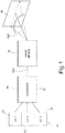
- Figure 1 shows a projective MEMS system 20, of a type in itself known, which includes a light source 22 formed, for example, by a plurality of laser diodes (LDs) 24, each of which emits electromagnetic radiation at a corresponding wavelength.
- LDs laser diodes
- FIG 1 illustrated in Figure 1 are three LDs 24, each of which emits radiation respectively in the red (620-750 nm), in the green (495-570 nm), and in the blue (450-475 nm).
- the projective MEMS system 20 further comprises a combiner 26, a MEMS device 30, and a screen 32.
- the combiner 26 is set downstream of the light source 22 for receiving the electromagnetic radiation emitted by the LDs 24 and form a single optical beam OB1, obtained by combination of said electromagnetic radiation.
- the combiner 26 is moreover designed to direct the optical beam OB1 onto the MEMS device 30.
- the MEMS device 30, described in greater detail hereinafter, is designed to generate a reflected optical beam OB2 and send the reflected optical beam OB2 onto the screen 32 for enabling formation of images on the screen 32.
- the MEMS device 30 is designed to vary in time the orientation in space of the axis of the reflected optical beam OB2 for scanning periodically portions of the screen 32; in particular, the reflected optical beam OB2 linearly scans possibly an entire portion of the screen 32.
- MEMS device 30 may find application in a system different from the one illustrated in Figure 1 .
- FIG. 2 shows an embodiment of the MEMS device 30 according to the present disclosure.
- the MEMS device 30 comprises a fixed supporting body 40, in particular made of semiconductor material, which includes a first structural region 44 and a second structural region 46.
- the MEMS device 30 is illustrated in an orthogonal reference system formed by three axes X, Y, Z. There is moreover defined an axis H parallel to the axis Z of the reference system.
- the first and second structural regions 44, 46 are arranged diametrally opposite with respect to the axis H, and aligned with one another along an axis O parallel to the axis X.
- the fixed supporting body 40 defines a cavity 52.
- the MEMS device 30 further comprises a mobile body 54 that is constrained to the first and second structural regions 44, 46 and is moreover suspended over the cavity 52.
- the mobile body 54 is mechanically coupled to the first and second structural regions 44, 46 by means, respectively, of a first deformable element 56 and a second deformable element 58, which are in particular configured to undergo a deformation of a torsional type.
- the mobile body 54 has a central portion 60, for example, circular in top plan view (in the horizontal plane XY), on which a mirror layer 65 is set, made of a material that has a high reflectivity for the light radiation to be projected, such as aluminium or gold.
- the central portion 60 is coupled to the first and second deformable elements 56, 58 by a respective first rigid connection region 55 and second rigid connection region 57.
- the first and second connection regions 55, 57 are directly and rigidly connected to the central portion 60 that houses the mirror layer 65.
- each of the first and second connection regions 55, 57 are considered "rigid" when it has a constant of torsional stiffness k higher than the constant of torsional stiffness of the first deformable element 56 or of the second deformable element 58, in particular an order of magnitude greater, more precisely twenty times greater, or more.
- both the first and second connection regions 55, 57 and the first and second deformable elements 56, 58 have a quadrangular cross section, in particular a rectangular cross section, with a thickness h and a width b such that h ⁇ b, in particular h ⁇ b.
- b/h 1 1.5 1.75 2 2.5 3 4 6 8 10 >10 ⁇ 7.09 5.10 4.67 4.37 4.02 3.72 3.56 3.34 3.26 3.19 3
- a first end 56a of the first deformable element 56 is fixed with respect to the first structural region 44, whereas a first end 58a of the second deformable element 58 is fixed with respect to the second structural region 46. Furthermore, a second end 56b of the first deformable element 56 and a second end 58b of the second deformable element 58 are fixed with respect to the first and second connection regions 55, 57, respectively.
- each of the first and second deformable elements 56, 58 has a shape of a parallelepiped, the dimension of which parallel to the axis X is greater than the corresponding dimensions along the axes Y and Z; for example, the dimension parallel to the axis X is at least five times greater than the dimensions along the axes Y and Z.
- each of the first and second deformable elements 56, 58 has two faces.
- the first and second deformable elements 56, 58 function, respectively, as first and second springs, since each of them can undergo a torsion about the axis O, and subsequently return to the position assumed in resting conditions.
- the shape of the first and second deformable elements 56, 58 bestows upon them a low torsional stiffness, for example, comprised between 10 -4 and 10 -3 N ⁇ m/rad.
- the mobile element 60 and the mirror 65 are thus designed to rotate, in use, about the axis O.
- first and second connection regions 55, 57 have a high torsional stiffness, for example, comprised between 10 -1 and 1 N ⁇ m/rad.
- the mobile body 54 has notches 61 and 62, in particular symmetrical with respect to the axis O.
- Each notch 61, 62 has a length L, and a width P.
- the thickness, along Z, of each notch 61, 62 is equal to the thickness, along Z, of the mobile body 54.
- the notches 61, 62 extend so that respective first terminal portions 61a, 62a are at a distance apart, measured along the axis Y, equal to or greater than the width, measured along the axis Y, of the first connection region 55.
- the notches 61, 62 moreover extend so that respective second terminal portions 61b, 62b are at a distance apart, measured along the axis Y, equal to or greater than the width, measured along the axis Y, of the second connection region 57.
- the central portion 60 that houses the mirror layer 65 is connected to the first and second deformable elements 56, 58 by portions made of semiconductor material having a width, along Y always equal to or greater than the width, along Y, of the first and second connection regions 55, 57. There is thus always guaranteed a rigid coupling of the central portion 60 with the first and second deformable elements 56, 58.
- each notch 61, 62 has, in top plan view, an arched curved shape that follows the circular profile of the perimetral edge of the mobile body 54.
- Each notch 61, 62 cuts the mobile body 54 along its entire thickness, thus defining frame regions 66, 68 that are separated from the central portion 60, and thus from the mirror layer 65, by the notch 61, 62, but are connected to the first connection region 55 and to the second connection region 57.
- the frame regions 66, 68 are coupled to the central portion 60 by the first and second connection regions 55, 57.
- a first actuator 70 and a second actuator 72 are arranged in the frame regions 66, 68.
- the first and second actuators 70, 72 extend following the curvature of the mobile body 54 and are symmetrical with respect to the axis O.
- the first and second actuators 70, 72 include a layer made of piezoelectric material set between control electrodes (not illustrated), in a per se known manner.
- the first and second actuators 70, 72 are illustrated with a dashed line in so far as, according to an embodiment, they are coated with a protective and electrically insulating layer, for example, made of dielectric material, such as silicon oxide.
- the first and second actuators 70, 72 have the function of triggering and maintaining the oscillation of the mobile body 54, each of them extends, in an embodiment, symmetrical with respect to an axis K passing through the centroid of the mobile body 54 (i.e., through the point of intersection between the axes O and H) and orthogonal to both of the axes O and H. In this way, no uncontrolled oscillations are generated, caused by a possible asymmetry of the actuators.
- FIG 3 shows, according to a further embodiment of the present disclosure, a MEMS device 30'; elements in common between the MEMS device 30 of Figure 2 and the MEMS device 30' of Figure 3 are designated by the same reference numbers and are not described any further herein.
- the first and second actuators 70, 72 are formed, respectively, by a plurality of piezoelectric sub-elements 70a, 70b and 72a, 72b.
- the piezoelectric sub-elements 70a, 70b extend symmetrically to one another with respect to the axis K, like the piezoelectric sub-elements 72a, 72b.
- the piezoelectric sub-element 70a is symmetrical to the piezoelectric sub-element 72a with respect to the axis O
- the piezoelectric sub-element 70b is symmetrical to the piezoelectric sub-element 72b with respect to the axis O.
- the driving voltage V 1 is applied to both of the piezoelectric sub-elements 70a, 70b, thus generating a local deformation of the frame region 66, which is directly transferred to the first and second connection regions 55, 57, imparting a rotation on the mobile body 54 about the axis O, thanks to the torsion of just the deformable elements 56, 58.
- the driving voltage V 2 is applied to both of the piezoelectric sub-elements 72a, 72b, thus generating a local deformation of the frame region 68, which is directly transferred to the first and second connection regions 55, 57, imparting a rotation on the mobile body 54 about the axis O, thanks to the torsion of just the deformable elements 56, 58.
- the central portion 60, the first and second connection regions 55, 57, the frame regions 66, 68, the first and second deformable elements 56, 58, and the first and second structural regions 44, 46 form a single piece; i.e., they belong to a monolithic structure, in particular made of semiconductor material obtained using known micromachining techniques. More in particular, the central portion 60, the first and second connection regions 55, 57, and the frame regions 66, 68 are coplanar with respect to one another.
- the first and second actuators 70, 72 include, in a per se known manner, a layer made of piezoelectric material, such as PVDF (polyvinylidene fluoride) or PZT (lead zirconate titanate), set between titanium/platinum electrodes, to form a stack.
- the first and second actuators 70, 72 are insulated from the layer of semiconductor material of the frame regions 66, 68 by a dielectric layer, such as silicon oxide, and are moreover coated with a further dielectric layer, for example of silicon oxide, acting as protective and electrically insulating layer.
- Electrical connections for example, in the form of conductive paths, extend in electrical contact with the electrodes of the first and second actuators 70, 72, for supplying the driving voltages V 1 and V 2 , respectively.
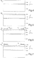
- Figures 4-10 are schematic illustrations of manufacturing steps for obtaining the MEMS device 30 of Figure 2 .
- the views of Figures 4-10 are side views, taken along a line of section coinciding with the axis K of Figure 2 .
- a wafer 100 is provided, for example of a SOI (Silicon Over Insulator) type, including a substrate 102 made of semiconductor material, such as silicon, an insulating layer 104, for example, of silicon oxide, which extends over the substrate 102, and a structural layer 106, which extends over the insulating layer 104.
- SOI Silicon Over Insulator
- a further insulating layer 108 is formed, made for example of silicon oxide formed by thermal oxidation, on the structural layer 106.
- first and second actuators 70, 72 are formed in a per se known manner, i.e., by depositing in succession a first electrode layer 110, a piezoelectric layer 112, and a second electrode layer 114, so that the piezoelectric layer 112 is sandwiched between the electrode layers 110, 114.
- the first and second actuators 70, 72 are then patterned by lithographic and etching steps.
- the dielectric layer 116 is then selectively removed from regions of the first and second actuators 70, 72 where openings for electrical access to the first and second actuators 70, 72 are to be formed (for contact of the electrodes 110, 114), and from regions of the wafer 100 where the mirror layer 65 is to be formed.
- a step of deposition, and subsequent lithographic and etching steps, of reflecting material (e.g., aluminium or gold) to form the mirror layer 65 is moreover carried out.
- the steps of formation of the electrical contacts 118, 120 and of the mirror layer 65 can be performed simultaneously. In this case, the electrical contacts 118, 120 will be made of the same material as the one chosen for the mirror layer 65.
- the structural layer 106 is etched for removing selective portions of the structural layer 106 in the regions where the notches 61, 62 are to be formed.
- Etching of the structural body 106 proceeds until the insulating layer 104 is reached, which has, in this context, the function of etch-stop layer.
- annular structure 122 underneath the central portion 60.
- the annular structure 122 is formed by portions of the substrate 102 and of the insulating layer 104 during the step of selective etching thereof discussed above.
- the annular structure 122 has the function of mechanical reinforcement of the structure 106, reducing deformation thereof during oscillation.
- the MEMS device 30 of Figure 2 is thus formed.
- a MEMS device 130 comprises frame regions 66, 68, which extend over a plane different from, and parallel to, the plane of lie of the central portion 60 and of the first and second connection regions 55, 57. More in particular, the frame regions 66, 68 extend above the central portion 60 and the first and second connection regions 55, 57.
- Figures 12 and 13 show intermediate manufacturing steps for obtaining the MEMS device 130 of Figures 11A and 11B .
- Manufacture of the MEMS device 130 envisages carrying out the steps already illustrated in Figures 4-7 and described with reference thereto.
- the step of Figure 12 is consequently subsequent to the step of Figure 7 .
- a step of etching of selective portions of the insulating layer 108 is carried out for removing the latter from the wafer 100, except for the portions thereof that extend underneath the actuators 70, 72. Surface regions of the structural layer 106 are thus exposed.
- the structural layer 106 is patterned (by lithography and etching) to form the frame regions 66, 68. It may be noted that, as is clearly visible from Figure 11A , in this embodiment the frame regions 66, 68 are connected together and form a monolithic annular path. The etching proceeds, possibly with a different etching chemistry, also on the underlying insulating layer 104, exposing surface regions of the substrate 102.
- deposited on the wafer 100 is a layer of reflecting material, for example, aluminium or gold, which is patterned by lithographic and etching steps in order to form the mirror layer 65.
- the mirror layer 65 extends, in this embodiment, over the surface of the substrate 102.
- a step of back-etching of the substrate 102 is carried out to release the MEMS structure, so rendering it free to oscillate according to its own degrees of freedom.
- the MEMS device 130 of Figure 11B Simultaneously with the step of etching of the substrate 102, the central portion 60, the first and second connection regions 55, 57, and the deformable elements 56, 58 are defined.
- the central portion 60, the first and second connection regions 55, 57, and the deformable elements 56, 58 are formed by appropriately patterned portions of the substrate 102, whereas the frame regions 66, 68 fixedly form with respect to one another a single ring obtained by patterning the structural layer 106.
- the first and second actuators 70, 72 extend over a plane raised with respect to the plane in which the mirror layer 65 extends.
- the first and second actuators 70, 72 moreover extend in a plane raised with respect to the plane of lie of the substrate 102, but rigidly connected thereto.
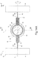
- a MEMS device 150 comprises frame regions 66, 68 that extend in a plane different from, and parallel to, the plane of lie of the central portion 60 and of the first and second connection regions 55, 57. More in particular, the frame regions 66, 68 extend underneath the central portion 60 and the first and second connection regions 55, 57.
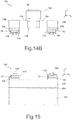
- Figures 15-17 show intermediate manufacturing steps for obtaining the MEMS device 150 of Figures 14A and 14B .
- Manufacture of the MEMS device 150 envisages carrying out the steps already illustrated in Figures 4-7 and described with reference thereto.
- the step of Figure 15 is consequently subsequent to the step of Figure 7 .
- a step of etching of selective portions of the insulating layer 108 is carried out for removing the latter from the wafer 100, except for the regions underlying the first and second actuators 70, 72. Surface regions of the structural layer 106 are thus exposed.
- the structural layer 106 is patterned for removing selective portions thereof, to form the frame regions 66, 68. It may be noted that, as is clearly visible from Figure 14A , the frame regions 66, 68 are connected together and form a monolithic annular path.
- the annular structure 152 is similar to the annular structure 122 and is formed by portions of the structural layer 106 and of the insulating layer 104 during the step of selective etching thereof, discussed above.
- the annular structure 152 has the same function as the annular structure 122.
- FIG 17 there follows a step of deposition of a layer of reflecting material on the back of the wafer 100, and subsequent patterning to form the mirror layer 65 of Figure 14A .
- the mirror layer 65 is formed, in particular, on the annular structure 152 (if present), i.e., overlying it when observed in the plane XY.
- the wafer 100 is rotated, thus obtaining the MEMS device 150 of Figure 14B .
- the central portion 60, the first and second connection regions 55, 57, and the deformable elements 56, 58 are defined.
- the central portion 60, the first and second connection regions 55, 57, and the deformable elements 56, 58 are formed by appropriately patterned portions of the substrate 102, whereas the frame regions 66, 68 form fixedly with respect to one another a single ring obtained by patterning the structural layer 106.
- the first and second actuators 70, 72 extend in a plane lowered with respect to the plane in which the mirror layer 65 extends.
- the first and second actuators 70, 72 moreover extend in a plane lowered with respect to the plane of lie of the substrate 102, but rigidly connected thereto.
- FIG. 18 shows a MEMS device 160 according to a further embodiment of the present disclosure. Elements of the MEMS device 160 in common with those of the MEMS devices 30, 30', 130 and 150 are designated by the same reference numbers.
- the MEMS device 160 does not have the frame regions 66, 68.
- the MEMS device 160 has, instead, a first cantilever structure 162 and a second cantilever structure 164, which are fixed with respect to the first coupling region 55 and the second coupling region 57, respectively.
- the first and second cantilever structures 162, 164 have, in a view in the plane XY, a rectangular shape with its main extension in the direction Y.
- the first cantilever structure 162 has two end terminals 162a, 162b, where a first actuator 168a and a second actuator 168b, of a piezoelectric type extend.
- the second cantilever structure 164 has two end terminals 164a, 164b, where a third actuator 169a and a fourth actuator 169b of a piezoelectric type extend.
- the driving voltage V 1 is applied to both the first and third actuators 168a, 169a, thus generating a local deformation of the first and second cantilever structures 162, 164, which is directly transferred to the first and second connection regions 55, 57, imparting a rotation on the mobile body 54 about the axis O thanks to the torsion of just the deformable elements 56, 58.
- the driving voltage V 2 is applied to both the second actuator 168b and the fourth actuator 169b, thus generating a respective local deformation of the first and second cantilever structures 162, 164, which is directly transferred to the first and second connection regions 55, 57, imparting a rotation on the mobile body 54 about the axis O thanks to the torsion of just the deformable elements 56, 58.
- the cantilever structures 162, 164 may have shapes different from the rectangular shape, for example any polygonal shape.
- the MEMS device further comprises an electronic control circuit (not illustrated), designed to start, and then maintain, oscillation of the mobile body 54.
- the electronic control circuit is configured to generate, in a per se known manner, the driving voltages V 1 , V 2 in the form, for example, of pulses.
- the driving voltages V 1 , V 2 in the form, for example, of pulses.
- the first actuator 70 or to the second actuator 72 reacts, causing a curving of the respective frame region 66, 68 with respect to which it is fixed.
- This curving action is directly transferred to the first and second coupling regions 55, 57 and, thus, to the first and second deformable elements 56, 58, thus generating a torsion thereof.
- a torque is generated, which keeps the mobile body 54 in oscillation.
- the mobile body 54 is made to oscillate at its resonance frequency.
- the electronic control circuit moreover manages triggering of the oscillation of the mobile body 54, starting from a state where the latter is stationary in resting condition.
- the present invention has been described, purely by way of example, with reference to the case of a MEMS device designed to reflect an optical beam in an electronically controllable way, and thus including at least a mirror.
- MEMS device designed to reflect an optical beam in an electronically controllable way, and thus including at least a mirror.
- the present invention can be applied to a different oscillating system, for example, MEMS resonators for generation of clock signals.
- the frames 66, 68 have always been illustrated and described as being circular in shape. It is evident that they may, however, have a different shape, for example, defining an oval path, or some other curvilinear path, or even a square path.
- the actuators 70 and 72 may not be present simultaneously.
- the MEMS device has only one between the first actuator 70 and the second actuator 72.
- just a pair of the actuators 70a, 70b and 72a, 72b may be present.
- the projective system 20 of Figure 1 may include, in addition to the MEMS device according to any embodiment of the present disclosure, also an additional MEMS device, set between the MEMS device 30 and the screen 32 and designed to receive the reflected optical beam OB2, to generate a further reflected optical beam, and to send this further reflected optical beam onto the screen 32.
- an additional MEMS device set between the MEMS device 30 and the screen 32 and designed to receive the reflected optical beam OB2, to generate a further reflected optical beam, and to send this further reflected optical beam onto the screen 32.
- the MEMS device 30 may likewise include also a movement device, for example of an electromagnetic type, designed to rotate the mobile element 60, and thus the mirror 65, about a further axis parallel, for example, to the axis Y.
- a movement device for example of an electromagnetic type, designed to rotate the mobile element 60, and thus the mirror 65, about a further axis parallel, for example, to the axis Y.
- At least one of the first and second deformable elements can be made of a material different from a semiconductor, such as, for example, a metal.
Landscapes
- Physics & Mathematics (AREA)
- General Physics & Mathematics (AREA)
- Optics & Photonics (AREA)
- Engineering & Computer Science (AREA)
- Manufacturing & Machinery (AREA)
- Micromachines (AREA)
- Mechanical Light Control Or Optical Switches (AREA)
- Piezo-Electric Or Mechanical Vibrators, Or Delay Or Filter Circuits (AREA)
- Piezo-Electric Transducers For Audible Bands (AREA)
Abstract
Description
- The present invention relates to an oscillating structure with piezoelectric actuation, to a system including the oscillating structure, and to a method for manufacturing the oscillating structure.
- Micromechanical mirror structures (or reflectors) are known made, at least in part, of semiconductor materials and obtain employing MEMS (Micro-Electro-Mechanical Systems) technology.
- MEMS reflectors are designed to receive an optical beam and to vary the direction of propagation thereof, in a periodic or quasi-periodic way. For this purpose, MEMS reflectors include mobile elements formed by mirrors, the positions of which in space are controlled electrically by appropriate oscillation control signals.
- In greater detail, in a generic MEMS reflector comprising a respective mirror, control of the position of the mirror is of particular importance to enable scanning of a portion of space with an optical beam, which is made to impinge on the mirror. In particular, control of the position of the mirror is determining in the case of resonant MEMS reflectors, where, in use, the mirror is made to oscillate in a substantially periodic way about a resting position, the period of oscillation being as close as possible to the resonance frequency of the mirror in order to maximize the angular distance covered by the mirror during each oscillation, and thus maximize the extent of the portion of space scanned.
- For instance, the patent application
US2011/0109951 describes a circuit to control of the position of the mirror of a MEMS reflector of a resonant type, said mirror being set for turning, under the action of an actuator of an electrostatic type, about an axis of rotation. In particular, the MEMS reflector according to the patent applicationUS2011/0109951 comprises a fixed supporting body, made of semiconductor material, and a mirror, which is constrained to the fixed supporting body by torsional springs. An actuator of an electrostatic type typically requires high operating voltages, higher than 150 V or currents in the region of 100 mA, thus limiting the energy efficiency of the final device. - The aim of the present invention is to provide an oscillating structure with reduced energy consumptions and, at the same time, optimized electromechanical efficiency. According to the present disclosure, moreover provided are a system including the oscillating structure and a method for manufacturing the oscillating structure.
- According to the present invention, an oscillating structure with piezoelectric actuation, a system including the oscillating structure, and a method for manufacturing the oscillating structure are thus provided as defined in the annexed claims.
- For a better understanding of the present invention preferred embodiments thereof are now described, purely by way of non-limiting examples, with reference to the attached drawings, wherein:
-
Figure 1 shows a block diagram of an electronic driving circuit of a MEMS reflector; -
Figure 2 shows, in top plan view, an oscillating structure according to an aspect of the present disclosure; -
Figure 3 shows, in top plan view, an oscillating structure according to a further aspect of the present disclosure; -
Figures 4-10 show, in lateral cross-sectional view, steps for manufacturing the oscillating structure ofFigure 2 ; -
Figures 11A and11B show, in top plan view and in lateral cross-sectional view respectively, an oscillating structure according to a further aspect of the present disclosure; -
Figures 12 and 13 show, in lateral cross-sectional view, intermediate manufacturing steps for obtaining the oscillating structure ofFigures 11A and11B ; -
Figures 14A and14B show, in top plan view and in lateral cross-sectional view respectively, an oscillating structure according to a further aspect of the present disclosure; -
Figures 15-17 show, in lateral cross-sectional view, intermediate manufacturing steps for obtaining the oscillating structure ofFigures 14A and14B ; and -
Figure 18 shows an oscillating structure according to a further embodiment of the present disclosure. -
Figure 1 shows a projective MEMS system 20, of a type in itself known, which includes alight source 22 formed, for example, by a plurality of laser diodes (LDs) 24, each of which emits electromagnetic radiation at a corresponding wavelength. For instance, illustrated inFigure 1 are threeLDs 24, each of which emits radiation respectively in the red (620-750 nm), in the green (495-570 nm), and in the blue (450-475 nm). - The projective MEMS system 20 further comprises a
combiner 26, aMEMS device 30, and ascreen 32. Thecombiner 26 is set downstream of thelight source 22 for receiving the electromagnetic radiation emitted by theLDs 24 and form a single optical beam OB1, obtained by combination of said electromagnetic radiation. Thecombiner 26 is moreover designed to direct the optical beam OB1 onto theMEMS device 30. In turn, theMEMS device 30, described in greater detail hereinafter, is designed to generate a reflected optical beam OB2 and send the reflected optical beam OB2 onto thescreen 32 for enabling formation of images on thescreen 32. - In detail, the
MEMS device 30 is designed to vary in time the orientation in space of the axis of the reflected optical beam OB2 for scanning periodically portions of thescreen 32; in particular, the reflected optical beam OB2 linearly scans possibly an entire portion of thescreen 32. - It is evident that the
MEMS device 30 may find application in a system different from the one illustrated inFigure 1 . -
Figure 2 shows an embodiment of theMEMS device 30 according to the present disclosure. - The
MEMS device 30 comprises a fixed supportingbody 40, in particular made of semiconductor material, which includes a firststructural region 44 and a secondstructural region 46. - The
MEMS device 30 is illustrated in an orthogonal reference system formed by three axes X, Y, Z. There is moreover defined an axis H parallel to the axis Z of the reference system. The first and secondstructural regions body 40 defines acavity 52. TheMEMS device 30 further comprises amobile body 54 that is constrained to the first and secondstructural regions cavity 52. - The
mobile body 54 is mechanically coupled to the first and secondstructural regions deformable element 56 and a seconddeformable element 58, which are in particular configured to undergo a deformation of a torsional type. Themobile body 54 has acentral portion 60, for example, circular in top plan view (in the horizontal plane XY), on which amirror layer 65 is set, made of a material that has a high reflectivity for the light radiation to be projected, such as aluminium or gold. Thecentral portion 60 is coupled to the first and seconddeformable elements rigid connection region 55 and secondrigid connection region 57. The first andsecond connection regions central portion 60 that houses themirror layer 65. In this context, each of the first andsecond connection regions deformable element 56 or of the seconddeformable element 58, in particular an order of magnitude greater, more precisely twenty times greater, or more. - Precisely, the constant of torsional stiffness k is defined by the following formula:

second connection regions deformable elements - The value of β can be obtained in approximate form from the formula β = (3n) / (n-0.63), with n = b/h, or else from tables available in technical manuals known to the person skilled in the branch, for example, a table of the type appearing below.
b/ h 1 1.5 1.75 2 2.5 3 4 6 8 10 >10 β 7.09 5.10 4.67 4.37 4.02 3.72 3.56 3.34 3.26 3.19 3 - To return to
Figure 2 , afirst end 56a of the firstdeformable element 56 is fixed with respect to the firststructural region 44, whereas afirst end 58a of the seconddeformable element 58 is fixed with respect to the secondstructural region 46. Furthermore, asecond end 56b of the firstdeformable element 56 and asecond end 58b of the seconddeformable element 58 are fixed with respect to the first andsecond connection regions - According to an embodiment, in resting conditions, each of the first and second
deformable elements deformable elements - For practical purposes, the first and second
deformable elements deformable elements deformable elements mobile element 60 and themirror 65 are thus designed to rotate, in use, about the axis O. - Instead, as has been said previously, the first and
second connection regions - In the embodiment illustrated in
Figure 2 , themobile body 54 hasnotches notch notch mobile body 54. - In any case, the
notches first terminal portions first connection region 55. Likewise, thenotches terminal portions second connection region 57. In this way, thecentral portion 60 that houses themirror layer 65 is connected to the first and seconddeformable elements second connection regions central portion 60 with the first and seconddeformable elements - In the embodiment illustrated in
Figure 2 , eachnotch mobile body 54. Eachnotch mobile body 54 along its entire thickness, thus definingframe regions central portion 60, and thus from themirror layer 65, by thenotch first connection region 55 and to thesecond connection region 57. Thus, theframe regions central portion 60 by the first andsecond connection regions - According to an aspect of the present disclosure, a
first actuator 70 and asecond actuator 72, of a piezoelectric type, are arranged in theframe regions second actuators mobile body 54 and are symmetrical with respect to the axis O. The first andsecond actuators Figure 2 , the first andsecond actuators second actuators mobile body 54, each of them extends, in an embodiment, symmetrical with respect to an axis K passing through the centroid of the mobile body 54 (i.e., through the point of intersection between the axes O and H) and orthogonal to both of the axes O and H. In this way, no uncontrolled oscillations are generated, caused by a possible asymmetry of the actuators. - In use, when a driving voltage V1 is applied to the
first actuator 70, a local deformation of theframe region 66 is generated, which is directly transferred to the first andsecond connection regions mobile body 54 about the axis O, thanks to the torsion of just thedeformable elements - Likewise, when a driving voltage V2 is applied to the
second actuator 72, a local deformation of theframe region 68 is generated that is directly transferred to the first andsecond connection regions mobile body 54 about the axis O, thanks to the torsion of just thedeformable elements -
Figure 3 shows, according to a further embodiment of the present disclosure, a MEMS device 30'; elements in common between theMEMS device 30 ofFigure 2 and the MEMS device 30' ofFigure 3 are designated by the same reference numbers and are not described any further herein. - In the embodiment of
Figure 3 , the first andsecond actuators - In use, the driving voltage V1 is applied to both of the piezoelectric sub-elements 70a, 70b, thus generating a local deformation of the
frame region 66, which is directly transferred to the first andsecond connection regions mobile body 54 about the axis O, thanks to the torsion of just thedeformable elements - Likewise, the driving voltage V2 is applied to both of the piezoelectric sub-elements 72a, 72b, thus generating a local deformation of the
frame region 68, which is directly transferred to the first andsecond connection regions mobile body 54 about the axis O, thanks to the torsion of just thedeformable elements - It is evident that, according to further embodiments (not illustrated), it is possible to form a larger number of piezoelectric sub-elements for each actuator.
- In an embodiment of the present disclosure, in particular as illustrated in
Figure 2 orFigure 3 , thecentral portion 60, the first andsecond connection regions frame regions deformable elements structural regions central portion 60, the first andsecond connection regions frame regions second actuators second actuators frame regions second actuators -
Figures 4-10 are schematic illustrations of manufacturing steps for obtaining theMEMS device 30 ofFigure 2 . The views ofFigures 4-10 are side views, taken along a line of section coinciding with the axis K ofFigure 2 . - With reference to
Figure 4 , awafer 100 is provided, for example of a SOI (Silicon Over Insulator) type, including asubstrate 102 made of semiconductor material, such as silicon, an insulatinglayer 104, for example, of silicon oxide, which extends over thesubstrate 102, and astructural layer 106, which extends over the insulatinglayer 104. - Then (
Figure 5 ), a further insulatinglayer 108 is formed, made for example of silicon oxide formed by thermal oxidation, on thestructural layer 106. - This is followed (
Figure 6 ) by formation of the first andsecond actuators first electrode layer 110, apiezoelectric layer 112, and asecond electrode layer 114, so that thepiezoelectric layer 112 is sandwiched between the electrode layers 110, 114. The first andsecond actuators - With reference to
Figure 7 , there follows a step of deposition, on thewafer 100, of adielectric layer 116 for protection of the first andsecond actuators - The
dielectric layer 116 is then selectively removed from regions of the first andsecond actuators second actuators electrodes 110, 114), and from regions of thewafer 100 where themirror layer 65 is to be formed. - This is followed by a step of deposition, and subsequent lithographic and etching steps, of conductive material, to form
electrical contacts second actuators mirror layer 65, is moreover carried out. The steps of formation of theelectrical contacts mirror layer 65 can be performed simultaneously. In this case, theelectrical contacts mirror layer 65. - Then (
Figure 9 ), thestructural layer 106 is etched for removing selective portions of thestructural layer 106 in the regions where thenotches mobile body 54 and of the first andsecond connection regions structural body 106 proceeds until the insulatinglayer 104 is reached, which has, in this context, the function of etch-stop layer. - Then (
Figure 10 ), there follows a step of back-etching of thewafer 100, to remove selective portions of thesubstrate 102 and of the insulatinglayer 104 underneath themobile body 54 and of the first andsecond connection regions - According to an aspect of the present disclosure, it is possible to form, optionally, an
annular structure 122 underneath thecentral portion 60. Theannular structure 122 is formed by portions of thesubstrate 102 and of the insulatinglayer 104 during the step of selective etching thereof discussed above. Theannular structure 122 has the function of mechanical reinforcement of thestructure 106, reducing deformation thereof during oscillation. - The
MEMS device 30 ofFigure 2 is thus formed. - In a further embodiment of the present disclosure, illustrated in
Figure 11A in top plan view and inFigure 11B in cross-sectional view along the line of section XI-XI ofFigure 11A , aMEMS device 130 comprisesframe regions central portion 60 and of the first andsecond connection regions frame regions central portion 60 and the first andsecond connection regions -
Figures 12 and 13 show intermediate manufacturing steps for obtaining theMEMS device 130 ofFigures 11A and11B . - Manufacture of the
MEMS device 130 envisages carrying out the steps already illustrated inFigures 4-7 and described with reference thereto. The step ofFigure 12 is consequently subsequent to the step ofFigure 7 . - With reference to
Figure 12 , after forming theelectrical contacts Figure 8 , a step of etching of selective portions of the insulatinglayer 108 is carried out for removing the latter from thewafer 100, except for the portions thereof that extend underneath theactuators structural layer 106 are thus exposed. - Then (
Figure 13 ), thestructural layer 106 is patterned (by lithography and etching) to form theframe regions Figure 11A , in this embodiment theframe regions layer 104, exposing surface regions of thesubstrate 102. - Then, deposited on the
wafer 100 is a layer of reflecting material, for example, aluminium or gold, which is patterned by lithographic and etching steps in order to form themirror layer 65. Themirror layer 65 extends, in this embodiment, over the surface of thesubstrate 102. - Finally, a step of back-etching of the
substrate 102 is carried out to release the MEMS structure, so rendering it free to oscillate according to its own degrees of freedom. There is thus obtained theMEMS device 130 ofFigure 11B . Simultaneously with the step of etching of thesubstrate 102, thecentral portion 60, the first andsecond connection regions deformable elements central portion 60, the first andsecond connection regions deformable elements substrate 102, whereas theframe regions structural layer 106. - As may be noted from
Figures 11A ,11B, and 13 , the first andsecond actuators mirror layer 65 extends. The first andsecond actuators substrate 102, but rigidly connected thereto. - In a further embodiment of the present disclosure (illustrated in
Figure 14A in top plan view and inFigure 14B in cross-sectional view along the line of section XIV-XIV ofFigure 14A ), aMEMS device 150 comprisesframe regions central portion 60 and of the first andsecond connection regions frame regions central portion 60 and the first andsecond connection regions -
Figures 15-17 show intermediate manufacturing steps for obtaining theMEMS device 150 ofFigures 14A and14B . - Manufacture of the
MEMS device 150 envisages carrying out the steps already illustrated inFigures 4-7 and described with reference thereto. The step ofFigure 15 is consequently subsequent to the step ofFigure 7 . - With reference to
Figure 15 , after forming theelectrical contacts Figure 8 , a step of etching of selective portions of the insulatinglayer 108 is carried out for removing the latter from thewafer 100, except for the regions underlying the first andsecond actuators structural layer 106 are thus exposed. - Next (
Figure 16 ), thestructural layer 106 is patterned for removing selective portions thereof, to form theframe regions Figure 14A , theframe regions annular structure 152 that extends over the insulatinglayer 104. Theannular structure 152 is similar to theannular structure 122 and is formed by portions of thestructural layer 106 and of the insulatinglayer 104 during the step of selective etching thereof, discussed above. Theannular structure 152 has the same function as theannular structure 122. - Then (
Figure 17 ), there follows a step of deposition of a layer of reflecting material on the back of thewafer 100, and subsequent patterning to form themirror layer 65 ofFigure 14A . Themirror layer 65 is formed, in particular, on the annular structure 152 (if present), i.e., overlying it when observed in the plane XY. - This is followed by steps of removal of selective portions of the
substrate 102, for releasing the MEMS structure, rendering it free to oscillate according to its own degrees of freedom. - The
wafer 100 is rotated, thus obtaining theMEMS device 150 ofFigure 14B . Simultaneously with the step of etching of thesubstrate 102, thecentral portion 60, the first andsecond connection regions deformable elements central portion 60, the first andsecond connection regions deformable elements substrate 102, whereas theframe regions structural layer 106. - As may be noted from
Figures 11A ,11B, and 13 , the first andsecond actuators mirror layer 65 extends. The first andsecond actuators substrate 102, but rigidly connected thereto. -
Figure 18 shows aMEMS device 160 according to a further embodiment of the present disclosure. Elements of theMEMS device 160 in common with those of theMEMS devices - The
MEMS device 160 does not have theframe regions MEMS device 160 has, instead, afirst cantilever structure 162 and asecond cantilever structure 164, which are fixed with respect to thefirst coupling region 55 and thesecond coupling region 57, respectively. The first andsecond cantilever structures first cantilever structure 162 has twoend terminals first actuator 168a and asecond actuator 168b, of a piezoelectric type extend. Likewise, thesecond cantilever structure 164 has twoend terminals third actuator 169a and afourth actuator 169b of a piezoelectric type extend. - In use, the driving voltage V1 is applied to both the first and
third actuators second cantilever structures second connection regions mobile body 54 about the axis O thanks to the torsion of just thedeformable elements - Likewise, the driving voltage V2 is applied to both the
second actuator 168b and thefourth actuator 169b, thus generating a respective local deformation of the first andsecond cantilever structures second connection regions mobile body 54 about the axis O thanks to the torsion of just thedeformable elements - It is evident that, according to further embodiments, the
cantilever structures - The MEMS device, according to any of the embodiments of the present disclosure, further comprises an electronic control circuit (not illustrated), designed to start, and then maintain, oscillation of the
mobile body 54. - The electronic control circuit is configured to generate, in a per se known manner, the driving voltages V1, V2 in the form, for example, of pulses. When a pulse is applied to the
first actuator 70 or to thesecond actuator 72, the latter reacts, causing a curving of therespective frame region second coupling regions deformable elements mobile body 54 in oscillation. - According to an embodiment, the
mobile body 54 is made to oscillate at its resonance frequency. - In use, according to an embodiment, assuming that the
mobile body 54 is oscillating and is at an angular distance +θmax, application to thefirst actuator 70 or to thesecond actuator 72 of a first electrical pulse causes generation of a torque that tends to bring themobile element 60 back into the resting position, with consequent reduction of the torsion to which the first and seconddeformable elements mobile body 60, on account of its own inertia, passes beyond the resting position, until an angular distance -θmax is reached, where a second electrical pulse is applied to the other one between the first andsecond actuators mobile body 60 back into the resting position, and so forth. The electrical pulses are thus distributed in time for keeping themobile body 60 in oscillation about the axis O. - The electronic control circuit moreover manages triggering of the oscillation of the
mobile body 54, starting from a state where the latter is stationary in resting condition. - Finally, it is clear that modifications and variations may be made to what has been described and illustrated herein, without thereby departing from the sphere of protection of the present invention, as defined in the annexed claims.
- Furthermore, the present invention has been described, purely by way of example, with reference to the case of a MEMS device designed to reflect an optical beam in an electronically controllable way, and thus including at least a mirror. However possible are other uses of the MEMS device described hereinafter. In general, the present invention can be applied to a different oscillating system, for example, MEMS resonators for generation of clock signals.
- Furthermore, the variant described with reference to
Figure 3 applies indifferently also to the embodiments described with reference toFigures 11a and14a . - Moreover, in the foregoing description and in the figures, the
frames - In addition, according to a further embodiment, the
actuators first actuator 70 and thesecond actuator 72. Likewise, in the case of the embodiment ofFigure 3 , just a pair of theactuators - It is moreover possible for the projective system 20 of
Figure 1 to include, in addition to the MEMS device according to any embodiment of the present disclosure, also an additional MEMS device, set between theMEMS device 30 and thescreen 32 and designed to receive the reflected optical beam OB2, to generate a further reflected optical beam, and to send this further reflected optical beam onto thescreen 32. In this way, it is possible to scan thescreen 32 with the aforesaid further reflected optical beam in a first direction and a second direction, for example, orthogonal to one another. - The
MEMS device 30 may likewise include also a movement device, for example of an electromagnetic type, designed to rotate themobile element 60, and thus themirror 65, about a further axis parallel, for example, to the axis Y. - Finally, it is possible for at least one of the first and second deformable elements to be made of a material different from a semiconductor, such as, for example, a metal.
Claims (22)
- An oscillating structure (30) with piezoelectric actuation, comprising:- a first torsional elastic element (56) and a second torsional elastic element (58) constrained to respective portions of a fixed supporting body (40) and defining an axis of rotation (O);- a mobile element (55, 57, 60) arranged between, and connected to, said first and second torsional elastic elements (56, 58), the mobile element being rotatable about the axis of rotation (O) as a consequence of a torsion of the first and second deformable elements; and- a first control region (66), which is coupled to the mobile element (55, 57, 60) and houses a first piezoelectric actuator (70), configured to cause, in use, a local deformation of the first control region (66) that generates a torsion of the first and second torsional elastic elements (56, 58).
- The oscillating structure according to claim 1, wherein said mobile element (55, 57, 60) comprises: a central body (60), a first connection region (55) between the central body (60) and the first torsional elastic element (56), and a second connection region (57) between the central body (60) and the second torsional elastic element (58),
said first control region (66) being fixed with respect to the first and second connection regions (55, 57) and separated from the central body (60) by a first trench (61). - The oscillating structure according to claim 2, wherein each of the first and second connection regions (55, 57) has a constant of torsional stiffness higher than the constant of torsional stiffness of each of the first and second torsional elastic elements (56, 58).
- The oscillating structure according to claim 3, wherein the constant of torsional stiffness of each of the first and second connection regions (55, 57) is at least an order of magnitude greater than the constant of torsional stiffness of each of the first and second torsional elastic elements (56, 58).
- The oscillating structure according to any of the preceding claims, further comprising a second control region (68) coupled to the mobile element (55, 57, 60) and housing a second piezoelectric actuator (72) configured to cause, in use, a local deformation of the second control region (68) that generates a torsion of the first and second torsional elastic elements (56, 58) opposite to the torsion generated, in use, by the first piezoelectric actuator (70).
- The oscillating structure according to claims 2 and 5, wherein said second control region (66) is fixed with respect to the first and second connection regions (55, 57) and separated from the central body (60) by a second trench (62).
- The oscillating structure according to any of claims 2-4 and 6, wherein the central body (60) houses a mirror (65), said oscillating structure forming a micro-mirror.
- The oscillating structure according to claims 1 and 5, wherein the first and second control regions (66, 68) are coplanar with the mobile element (55, 57, 60).
- The oscillating structure according to claims 1 and 5, wherein the first and second control regions (66, 68) extend in a plane parallel to the plane of lie of the mobile element (55, 57, 60), at a height lower than the plane of lie of the mobile element.
- The oscillating structure according to claims 1 and 5, wherein the first and second control regions (66, 68) extend in a plane parallel to the plane of lie of the mobile element (55, 57, 60), at a height greater than the plane of lie of the mobile element.
- The oscillating structure according to any of the preceding claims, further comprising an electronic circuit operatively coupled to the first piezoelectric actuator (70), configured to bias the first piezoelectric actuator (70) at a driving voltage such as to generate, and maintain, an oscillation of the mobile element (55, 57, 60).
- A projective MEMS system comprising:an oscillating structure (30) according to any of claims 1-11;a reflecting element (65), constrained to the mobile element (60), designed to reflect a light beam;a light source (22, 26) that can be operated for generating the incident light beam on said reflecting element (65); andan image-generating module (32), operatively coupled to said oscillating structure (30), for generating part of an image associated to a light beam reflected by said reflecting element (65).
- A method for manufacturing an oscillating structure (30) with piezoelectric actuation, comprising the steps of:- forming a first torsional elastic element (56) and a second torsional elastic element (58) constrained to respective portions of a fixed supporting body (40) and defining an axis of rotation (O);- forming a mobile element (55, 57, 60) between, and connected to, said first and second torsional elastic elements (56, 58), the mobile element being rotatable about the axis of rotation (O) as a consequence of a torsion of the first and second deformable elements;forming a first control region (66) coupled to the mobile element (55, 57, 60); and
forming a first piezoelectric actuator (70) coupled to the first control region (66) and configured to cause, in use, a local deformation of the first control region (66) that generates a torsion of the first and second torsional elastic elements (56, 58). - The method according to claim 13, wherein the step of forming said mobile element (55, 57, 60) comprises the steps of: forming a central body (60); forming a first connection region (55) between the central body (60) and the first torsional elastic element (56); and forming a second connection region (57) between the central body (60) and the second torsional elastic element (58),
the step of forming said first control region (66) including forming the first control region (66) fixed with respect to the first and second connection regions (55, 57) and forming a first trench (61) for separating the first control region (66) from the central body (60). - The method according to claim 14, wherein forming the first and second connection regions (55, 57) includes forming the first and second connection regions (55, 57) with a constant of torsional stiffness greater than the constant of torsional stiffness of each of the first and second torsional elastic elements (56, 58).
- The method according to claim 15, further comprising the step of patterning each of the first and second connection regions (55, 57) so that they have a respective constant of torsional stiffness at least one order of magnitude higher than the constant of torsional stiffness of each of the first and second torsional elastic elements (56, 58).
- The method according to any of claims 13-16, further comprising the steps of:forming a second control region (68) coupled to the mobile element (55, 57, 60); andforming a second piezoelectric actuator (72) coupled to the second control region (68) and configured to cause, in use, a local deformation of the second control region (68) that generates a torsion of the first and second torsional elastic elements (56, 58) opposite to the torsion generated by the first piezoelectric actuator (70).
- The method according to claims 14 and 17, wherein the step of forming said second control region (66) includes: forming the second control region (66) fixed with respect to the first and second connection regions (55, 57); and forming a second trench (62) for separating the second control region (66) from the central body (60).
- The method according to any of claims 14-16 and 18, wherein forming the central body (60) includes depositing a mirror layer (65), so that said oscillating structure forms a micro-mirror.
- The method according to claims 13 and 17, wherein the steps of forming the first and second control regions (66, 68) are carried out simultaneously with the steps of forming the mobile element (55, 57, 60), said first and second control regions (66, 68) being formed coplanar with the mobile element (55, 57, 60).
- The method according to claims 13 and 17, wherein the steps of forming the first and second control regions (66, 68) include photolithographically defining a layer of semiconductor material, which extends at a height lower than the plane of lie of the mobile element.
- The method according to claims 13 and 17, wherein the steps of forming the first and second control regions (66, 68) include photolithographically defining a layer of semiconductor material, which extends at a height greater than the plane of lie of the mobile element.
Applications Claiming Priority (1)
| Application Number | Priority Date | Filing Date | Title |
|---|---|---|---|
| IT102016000079604A IT201600079604A1 (en) | 2016-07-28 | 2016-07-28 | OSCILLATING STRUCTURE WITH PIEZOELECTRIC IMPLEMENTATION, SYSTEM AND MANUFACTURING METHOD |
Publications (2)
| Publication Number | Publication Date |
|---|---|
| EP3276391A1 true EP3276391A1 (en) | 2018-01-31 |
| EP3276391B1 EP3276391B1 (en) | 2021-08-18 |
Family
ID=57610220
Family Applications (1)
| Application Number | Title | Priority Date | Filing Date |
|---|---|---|---|
| EP17162612.0A Active EP3276391B1 (en) | 2016-07-28 | 2017-03-23 | Oscillating structure with piezoelectric actuation, system and manufacturing method |
Country Status (4)
| Country | Link |
|---|---|
| US (1) | US10365475B2 (en) |
| EP (1) | EP3276391B1 (en) |
| CN (2) | CN206757183U (en) |
| IT (1) | IT201600079604A1 (en) |
Families Citing this family (14)
| Publication number | Priority date | Publication date | Assignee | Title |
|---|---|---|---|---|
| IT201600079604A1 (en) * | 2016-07-28 | 2018-01-28 | St Microelectronics Srl | OSCILLATING STRUCTURE WITH PIEZOELECTRIC IMPLEMENTATION, SYSTEM AND MANUFACTURING METHOD |
| US10384239B2 (en) | 2016-09-27 | 2019-08-20 | Texas Instruments Incorporated | Methods and apparatus for ultrasonic lens cleaner using configurable filter banks |
| DE102018216611B4 (en) * | 2018-05-22 | 2022-01-05 | Infineon Technologies Ag | MEMS component with suspension structure and method for manufacturing a MEMS component |
| DE102018220422A1 (en) * | 2018-11-28 | 2020-05-28 | Robert Bosch Gmbh | Actuation device for a micromechanical component, micromechanical component and method for producing a micromechanical component |
| IT201900004199A1 (en) * | 2019-03-22 | 2020-09-22 | St Microelectronics Srl | MICROELECTROMECHANICAL STRUCTURE OF BIAXIAL RESONANT MIRROR WITH PIEZOELECTRIC ACTUATION WITH IMPROVED CHARACTERISTICS |
| EP3748562A1 (en) | 2019-05-08 | 2020-12-09 | EXFO Solutions SAS | Timeline visualization & investigation systems and methods for time lasting events |
| IT201900024469A1 (en) * | 2019-12-18 | 2021-06-18 | St Microelectronics Srl | MICROELECTROMECHANICAL MIRROR DEVICE WITH PIEZOELECTRIC ACTUATION, WITH IMPROVED STRUCTURE |
| IT202000001411A1 (en) * | 2020-01-24 | 2021-07-24 | St Microelectronics Srl | PROCESSING METHOD OF A SLICE FOR THE MANUFACTURE OF AN OSCILLATING STRUCTURE SUCH AS A MICRO-MIRROR |
| US12001012B2 (en) | 2021-04-23 | 2024-06-04 | Stmicroelectronics S.R.L. | Piezoelectric based MEMS device with time sharing actuation and sensing circuitry |
| IT202100011039A1 (en) | 2021-04-30 | 2022-10-30 | St Microelectronics Srl | PROCEDURE FOR MANUFACTURING A MIRROR MICROELECTROMECHANICAL DEVICE AND MIRROR MICROELECTROMECHANICAL DEVICE |
| CN115268059A (en) * | 2021-04-30 | 2022-11-01 | 意法半导体股份有限公司 | Method for manufacturing a microelectromechanical mirror device and microelectromechanical mirror device |
| DE102022200149A1 (en) | 2022-01-10 | 2023-07-13 | Robert Bosch Gesellschaft mit beschränkter Haftung | Micromechanical component |
| CN114994907A (en) * | 2022-05-30 | 2022-09-02 | 成都英飞睿技术有限公司 | Rapid scanning reflector, flexible supporting structure and mounting method thereof |
| CN117277866B (en) * | 2023-11-22 | 2024-01-23 | 吉林大学 | Four-degree-of-freedom trans-scale stepping actuator based on piezoelectric driving |
Citations (8)
| Publication number | Priority date | Publication date | Assignee | Title |
|---|---|---|---|---|
| JP2006081320A (en) * | 2004-09-09 | 2006-03-23 | Seiko Epson Corp | Actuator |
| JP2010204142A (en) * | 2009-02-27 | 2010-09-16 | Ricoh Co Ltd | Optical deflector, optical scanner and image forming apparatus |
| US20110109951A1 (en) | 2009-10-29 | 2011-05-12 | Btendo | Method and device for monitoring movement of mirrors in a mems device |
| WO2012133505A1 (en) * | 2011-03-31 | 2012-10-04 | ブラザー工業株式会社 | Optical scanner and manufacturing method for optical scanner |
| EP2706393A1 (en) * | 2012-09-11 | 2014-03-12 | Stanley Electric Co., Ltd. | Optical deflector including narrow piezoelectric sensor element between torsion bar and piezoelectric actuator |
| EP2808719A1 (en) * | 2013-05-28 | 2014-12-03 | Stanley Electric Co., Ltd. | Optical deflector including separated piezoelectric portions on piezoelectric actuators and its designing method |
| US20150062677A1 (en) * | 2013-08-28 | 2015-03-05 | Robert Bosch Gmbh | Micromechanical component and method for producing a micromechanical component |
| US20150175054A1 (en) * | 2013-12-25 | 2015-06-25 | Stanley Electric Co., Ltd. | Optical deflector apparatus and vehicle headlight including the same |
Family Cites Families (12)
| Publication number | Priority date | Publication date | Assignee | Title |
|---|---|---|---|---|
| US6900918B2 (en) * | 2002-07-08 | 2005-05-31 | Texas Instruments Incorporated | Torsionally hinged devices with support anchors |
| ATE361481T1 (en) * | 2003-07-14 | 2007-05-15 | Koninkl Philips Electronics Nv | LASER BEAM SCANNER |
| JP5444968B2 (en) * | 2009-05-11 | 2014-03-19 | ミツミ電機株式会社 | Actuator and optical scanning device using the same |
| US9122059B2 (en) * | 2010-11-24 | 2015-09-01 | Nec Corporation | Optical scanning device |
| US9105834B2 (en) | 2012-01-27 | 2015-08-11 | Microvision, Inc. | Piezoelectric actuated device, method and system |
| ITTO20120758A1 (en) * | 2012-08-31 | 2014-03-01 | St Microelectronics Srl | MEMS DEVICE INCLUDING A MOBILE ELEMENT AND A RESISTIVE SENSOR, AND GENERATION METHOD OF AN INDICATIVE SIGNAL OF THE POSITION OF THE MOBILE ELEMENT |
| JP5843808B2 (en) * | 2013-05-31 | 2016-01-13 | 京セラドキュメントソリューションズ株式会社 | Sheet conveying apparatus, image reading apparatus, and image forming apparatus |
| JP6253915B2 (en) * | 2013-08-01 | 2017-12-27 | 浜松ホトニクス株式会社 | Actuator device and mirror drive device |
| JP6289957B2 (en) * | 2014-03-25 | 2018-03-07 | スタンレー電気株式会社 | Optical deflector |
| JP6349229B2 (en) * | 2014-10-23 | 2018-06-27 | スタンレー電気株式会社 | Biaxial optical deflector and manufacturing method thereof |
| CN105403997A (en) * | 2015-11-19 | 2016-03-16 | 苏州工业园区纳米产业技术研究院有限公司 | Piezoelectric driving two-dimensional scanning micro-mirror |
| IT201600079604A1 (en) * | 2016-07-28 | 2018-01-28 | St Microelectronics Srl | OSCILLATING STRUCTURE WITH PIEZOELECTRIC IMPLEMENTATION, SYSTEM AND MANUFACTURING METHOD |
-
2016
- 2016-07-28 IT IT102016000079604A patent/IT201600079604A1/en unknown
-
2017
- 2017-03-22 US US15/465,742 patent/US10365475B2/en active Active
- 2017-03-22 CN CN201720285939.6U patent/CN206757183U/en not_active Withdrawn - After Issue
- 2017-03-22 CN CN201710173576.1A patent/CN107664836B/en active Active
- 2017-03-23 EP EP17162612.0A patent/EP3276391B1/en active Active
Patent Citations (8)
| Publication number | Priority date | Publication date | Assignee | Title |
|---|---|---|---|---|
| JP2006081320A (en) * | 2004-09-09 | 2006-03-23 | Seiko Epson Corp | Actuator |
| JP2010204142A (en) * | 2009-02-27 | 2010-09-16 | Ricoh Co Ltd | Optical deflector, optical scanner and image forming apparatus |
| US20110109951A1 (en) | 2009-10-29 | 2011-05-12 | Btendo | Method and device for monitoring movement of mirrors in a mems device |
| WO2012133505A1 (en) * | 2011-03-31 | 2012-10-04 | ブラザー工業株式会社 | Optical scanner and manufacturing method for optical scanner |
| EP2706393A1 (en) * | 2012-09-11 | 2014-03-12 | Stanley Electric Co., Ltd. | Optical deflector including narrow piezoelectric sensor element between torsion bar and piezoelectric actuator |
| EP2808719A1 (en) * | 2013-05-28 | 2014-12-03 | Stanley Electric Co., Ltd. | Optical deflector including separated piezoelectric portions on piezoelectric actuators and its designing method |
| US20150062677A1 (en) * | 2013-08-28 | 2015-03-05 | Robert Bosch Gmbh | Micromechanical component and method for producing a micromechanical component |
| US20150175054A1 (en) * | 2013-12-25 | 2015-06-25 | Stanley Electric Co., Ltd. | Optical deflector apparatus and vehicle headlight including the same |
Also Published As
| Publication number | Publication date |
|---|---|
| CN206757183U (en) | 2017-12-15 |
| CN107664836B (en) | 2020-12-25 |
| EP3276391B1 (en) | 2021-08-18 |
| US20180031823A1 (en) | 2018-02-01 |
| US10365475B2 (en) | 2019-07-30 |
| IT201600079604A1 (en) | 2018-01-28 |
| CN107664836A (en) | 2018-02-06 |
Similar Documents
| Publication | Publication Date | Title |
|---|---|---|
| EP3276391B1 (en) | Oscillating structure with piezoelectric actuation, system and manufacturing method | |
| JP6447683B2 (en) | Scanning microelectromechanical reflector system, light detection and ranging (LIDAR) device, and method of operating scanning microelectromechanical reflector system | |
| US8456727B2 (en) | Actuator device for optical deflector | |
| US6014240A (en) | Method and apparatus for an integrated laser beam scanner using a carrier substrate | |
| US6002507A (en) | Method and apparatus for an integrated laser beam scanner | |
| US6091537A (en) | Electro-actuated microlens assemblies | |
| US5914801A (en) | Microelectromechanical devices including rotating plates and related methods | |
| US10197794B2 (en) | Micro-electro-mechanical device with a movable structure, in particular micromirror, and manufacturing process thereof | |
| US9335543B2 (en) | Optical scanner, image display device, head mount display, and heads-up display | |
| US8553306B2 (en) | Optical deflector and optical device | |
| JP4351586B2 (en) | Optical scanner having curved mirror and method for manufacturing the same | |
| EP3392696A1 (en) | Oscillating structure with reduced dynamic deformation, optical device including the oscillating structure, and method of manufacturing the oscillating structure | |
| TW201110274A (en) | Mems device | |
| JP2009093120A (en) | Optical reflection element | |
| JPH10239601A (en) | Thin-film optical path adjusting device and method of manufacturing the same | |
| JP2011069954A (en) | Optical scanner | |
| US20200233205A1 (en) | Optical scanning device and method of manufacturing the same | |
| EP3854751B1 (en) | Method of processing a wafer for manufacturing an oscillating structure such as a micro-mirror | |
| US20230359022A1 (en) | Deflection device with a mirror for use in scanner technical field | |
| US12313840B2 (en) | Optical scanning device, distance measuring device, and method for manufacturing optical scanning device | |
| EP4310573B1 (en) | Mems mirror device with piezoelectric actuation and manufacturing process thereof | |
| JP3537408B2 (en) | Microactuator for optical switching and method of manufacturing the same | |
| PL178495B1 (en) | System of thin-film mirrors formed at low temperature | |
| KR100233372B1 (en) | Fabrication method of thin film actuated mirror array | |
| KR0154923B1 (en) | Method for manufacturing optical path control apparatus |
Legal Events
| Date | Code | Title | Description |
|---|---|---|---|
| PUAI | Public reference made under article 153(3) epc to a published international application that has entered the european phase |
Free format text: ORIGINAL CODE: 0009012 |
|
| STAA | Information on the status of an ep patent application or granted ep patent |
Free format text: STATUS: THE APPLICATION HAS BEEN PUBLISHED |
|
| AK | Designated contracting states |
Kind code of ref document: A1 Designated state(s): AL AT BE BG CH CY CZ DE DK EE ES FI FR GB GR HR HU IE IS IT LI LT LU LV MC MK MT NL NO PL PT RO RS SE SI SK SM TR |
|
| AX | Request for extension of the european patent |
Extension state: BA ME |
|
| STAA | Information on the status of an ep patent application or granted ep patent |
Free format text: STATUS: REQUEST FOR EXAMINATION WAS MADE |
|
| 17P | Request for examination filed |
Effective date: 20180716 |
|
| RBV | Designated contracting states (corrected) |
Designated state(s): AL AT BE BG CH CY CZ DE DK EE ES FI FR GB GR HR HU IE IS IT LI LT LU LV MC MK MT NL NO PL PT RO RS SE SI SK SM TR |
|
| STAA | Information on the status of an ep patent application or granted ep patent |
Free format text: STATUS: EXAMINATION IS IN PROGRESS |
|
| 17Q | First examination report despatched |
Effective date: 20200330 |
|
| GRAP | Despatch of communication of intention to grant a patent |
Free format text: ORIGINAL CODE: EPIDOSNIGR1 |
|
| STAA | Information on the status of an ep patent application or granted ep patent |
Free format text: STATUS: GRANT OF PATENT IS INTENDED |
|
| INTG | Intention to grant announced |
Effective date: 20210309 |
|
| GRAS | Grant fee paid |
Free format text: ORIGINAL CODE: EPIDOSNIGR3 |
|
| GRAA | (expected) grant |
Free format text: ORIGINAL CODE: 0009210 |
|
| STAA | Information on the status of an ep patent application or granted ep patent |
Free format text: STATUS: THE PATENT HAS BEEN GRANTED |
|
| AK | Designated contracting states |
Kind code of ref document: B1 Designated state(s): AL AT BE BG CH CY CZ DE DK EE ES FI FR GB GR HR HU IE IS IT LI LT LU LV MC MK MT NL NO PL PT RO RS SE SI SK SM TR |
|
| REG | Reference to a national code |
Ref country code: GB Ref legal event code: FG4D |
|
| REG | Reference to a national code |
Ref country code: CH Ref legal event code: EP |
|
| REG | Reference to a national code |
Ref country code: DE Ref legal event code: R096 Ref document number: 602017044130 Country of ref document: DE |
|
| REG | Reference to a national code |
Ref country code: IE Ref legal event code: FG4D Ref country code: AT Ref legal event code: REF Ref document number: 1422154 Country of ref document: AT Kind code of ref document: T Effective date: 20210915 |
|
| REG | Reference to a national code |
Ref country code: LT Ref legal event code: MG9D |
|
| REG | Reference to a national code |
Ref country code: NL Ref legal event code: MP Effective date: 20210818 |
|
| REG | Reference to a national code |
Ref country code: AT Ref legal event code: MK05 Ref document number: 1422154 Country of ref document: AT Kind code of ref document: T Effective date: 20210818 |
|
| PG25 | Lapsed in a contracting state [announced via postgrant information from national office to epo] |
Ref country code: RS Free format text: LAPSE BECAUSE OF FAILURE TO SUBMIT A TRANSLATION OF THE DESCRIPTION OR TO PAY THE FEE WITHIN THE PRESCRIBED TIME-LIMIT Effective date: 20210818 Ref country code: SE Free format text: LAPSE BECAUSE OF FAILURE TO SUBMIT A TRANSLATION OF THE DESCRIPTION OR TO PAY THE FEE WITHIN THE PRESCRIBED TIME-LIMIT Effective date: 20210818 Ref country code: LT Free format text: LAPSE BECAUSE OF FAILURE TO SUBMIT A TRANSLATION OF THE DESCRIPTION OR TO PAY THE FEE WITHIN THE PRESCRIBED TIME-LIMIT Effective date: 20210818 Ref country code: AT Free format text: LAPSE BECAUSE OF FAILURE TO SUBMIT A TRANSLATION OF THE DESCRIPTION OR TO PAY THE FEE WITHIN THE PRESCRIBED TIME-LIMIT Effective date: 20210818 Ref country code: BG Free format text: LAPSE BECAUSE OF FAILURE TO SUBMIT A TRANSLATION OF THE DESCRIPTION OR TO PAY THE FEE WITHIN THE PRESCRIBED TIME-LIMIT Effective date: 20211118 Ref country code: PT Free format text: LAPSE BECAUSE OF FAILURE TO SUBMIT A TRANSLATION OF THE DESCRIPTION OR TO PAY THE FEE WITHIN THE PRESCRIBED TIME-LIMIT Effective date: 20211220 Ref country code: NO Free format text: LAPSE BECAUSE OF FAILURE TO SUBMIT A TRANSLATION OF THE DESCRIPTION OR TO PAY THE FEE WITHIN THE PRESCRIBED TIME-LIMIT Effective date: 20211118 Ref country code: ES Free format text: LAPSE BECAUSE OF FAILURE TO SUBMIT A TRANSLATION OF THE DESCRIPTION OR TO PAY THE FEE WITHIN THE PRESCRIBED TIME-LIMIT Effective date: 20210818 Ref country code: FI Free format text: LAPSE BECAUSE OF FAILURE TO SUBMIT A TRANSLATION OF THE DESCRIPTION OR TO PAY THE FEE WITHIN THE PRESCRIBED TIME-LIMIT Effective date: 20210818 Ref country code: HR Free format text: LAPSE BECAUSE OF FAILURE TO SUBMIT A TRANSLATION OF THE DESCRIPTION OR TO PAY THE FEE WITHIN THE PRESCRIBED TIME-LIMIT Effective date: 20210818 |
|
| PG25 | Lapsed in a contracting state [announced via postgrant information from national office to epo] |
Ref country code: PL Free format text: LAPSE BECAUSE OF FAILURE TO SUBMIT A TRANSLATION OF THE DESCRIPTION OR TO PAY THE FEE WITHIN THE PRESCRIBED TIME-LIMIT Effective date: 20210818 Ref country code: LV Free format text: LAPSE BECAUSE OF FAILURE TO SUBMIT A TRANSLATION OF THE DESCRIPTION OR TO PAY THE FEE WITHIN THE PRESCRIBED TIME-LIMIT Effective date: 20210818 Ref country code: GR Free format text: LAPSE BECAUSE OF FAILURE TO SUBMIT A TRANSLATION OF THE DESCRIPTION OR TO PAY THE FEE WITHIN THE PRESCRIBED TIME-LIMIT Effective date: 20211119 |
|
| PG25 | Lapsed in a contracting state [announced via postgrant information from national office to epo] |
Ref country code: NL Free format text: LAPSE BECAUSE OF FAILURE TO SUBMIT A TRANSLATION OF THE DESCRIPTION OR TO PAY THE FEE WITHIN THE PRESCRIBED TIME-LIMIT Effective date: 20210818 |
|
| PG25 | Lapsed in a contracting state [announced via postgrant information from national office to epo] |
Ref country code: DK Free format text: LAPSE BECAUSE OF FAILURE TO SUBMIT A TRANSLATION OF THE DESCRIPTION OR TO PAY THE FEE WITHIN THE PRESCRIBED TIME-LIMIT Effective date: 20210818 |
|
| REG | Reference to a national code |
Ref country code: DE Ref legal event code: R097 Ref document number: 602017044130 Country of ref document: DE |
|
| PG25 | Lapsed in a contracting state [announced via postgrant information from national office to epo] |
Ref country code: SM Free format text: LAPSE BECAUSE OF FAILURE TO SUBMIT A TRANSLATION OF THE DESCRIPTION OR TO PAY THE FEE WITHIN THE PRESCRIBED TIME-LIMIT Effective date: 20210818 Ref country code: SK Free format text: LAPSE BECAUSE OF FAILURE TO SUBMIT A TRANSLATION OF THE DESCRIPTION OR TO PAY THE FEE WITHIN THE PRESCRIBED TIME-LIMIT Effective date: 20210818 Ref country code: RO Free format text: LAPSE BECAUSE OF FAILURE TO SUBMIT A TRANSLATION OF THE DESCRIPTION OR TO PAY THE FEE WITHIN THE PRESCRIBED TIME-LIMIT Effective date: 20210818 Ref country code: EE Free format text: LAPSE BECAUSE OF FAILURE TO SUBMIT A TRANSLATION OF THE DESCRIPTION OR TO PAY THE FEE WITHIN THE PRESCRIBED TIME-LIMIT Effective date: 20210818 Ref country code: CZ Free format text: LAPSE BECAUSE OF FAILURE TO SUBMIT A TRANSLATION OF THE DESCRIPTION OR TO PAY THE FEE WITHIN THE PRESCRIBED TIME-LIMIT Effective date: 20210818 Ref country code: AL Free format text: LAPSE BECAUSE OF FAILURE TO SUBMIT A TRANSLATION OF THE DESCRIPTION OR TO PAY THE FEE WITHIN THE PRESCRIBED TIME-LIMIT Effective date: 20210818 |
|
| PLBE | No opposition filed within time limit |
Free format text: ORIGINAL CODE: 0009261 |
|
| STAA | Information on the status of an ep patent application or granted ep patent |
Free format text: STATUS: NO OPPOSITION FILED WITHIN TIME LIMIT |
|
| 26N | No opposition filed |
Effective date: 20220519 |
|
| PG25 | Lapsed in a contracting state [announced via postgrant information from national office to epo] |
Ref country code: IT Free format text: LAPSE BECAUSE OF FAILURE TO SUBMIT A TRANSLATION OF THE DESCRIPTION OR TO PAY THE FEE WITHIN THE PRESCRIBED TIME-LIMIT Effective date: 20210818 |
|
| PG25 | Lapsed in a contracting state [announced via postgrant information from national office to epo] |
Ref country code: SI Free format text: LAPSE BECAUSE OF FAILURE TO SUBMIT A TRANSLATION OF THE DESCRIPTION OR TO PAY THE FEE WITHIN THE PRESCRIBED TIME-LIMIT Effective date: 20210818 |
|
| PG25 | Lapsed in a contracting state [announced via postgrant information from national office to epo] |
Ref country code: MC Free format text: LAPSE BECAUSE OF FAILURE TO SUBMIT A TRANSLATION OF THE DESCRIPTION OR TO PAY THE FEE WITHIN THE PRESCRIBED TIME-LIMIT Effective date: 20210818 |
|
| REG | Reference to a national code |
Ref country code: CH Ref legal event code: PL |
|
| GBPC | Gb: european patent ceased through non-payment of renewal fee |
Effective date: 20220323 |
|
| REG | Reference to a national code |
Ref country code: BE Ref legal event code: MM Effective date: 20220331 |
|
| PG25 | Lapsed in a contracting state [announced via postgrant information from national office to epo] |
Ref country code: LU Free format text: LAPSE BECAUSE OF NON-PAYMENT OF DUE FEES Effective date: 20220323 Ref country code: LI Free format text: LAPSE BECAUSE OF NON-PAYMENT OF DUE FEES Effective date: 20220331 Ref country code: IE Free format text: LAPSE BECAUSE OF NON-PAYMENT OF DUE FEES Effective date: 20220323 Ref country code: GB Free format text: LAPSE BECAUSE OF NON-PAYMENT OF DUE FEES Effective date: 20220323 Ref country code: FR Free format text: LAPSE BECAUSE OF NON-PAYMENT OF DUE FEES Effective date: 20220331 Ref country code: CH Free format text: LAPSE BECAUSE OF NON-PAYMENT OF DUE FEES Effective date: 20220331 |
|
| PG25 | Lapsed in a contracting state [announced via postgrant information from national office to epo] |
Ref country code: BE Free format text: LAPSE BECAUSE OF NON-PAYMENT OF DUE FEES Effective date: 20220331 |
|
| PG25 | Lapsed in a contracting state [announced via postgrant information from national office to epo] |
Ref country code: HU Free format text: LAPSE BECAUSE OF FAILURE TO SUBMIT A TRANSLATION OF THE DESCRIPTION OR TO PAY THE FEE WITHIN THE PRESCRIBED TIME-LIMIT; INVALID AB INITIO Effective date: 20170323 |
|
| PG25 | Lapsed in a contracting state [announced via postgrant information from national office to epo] |
Ref country code: MK Free format text: LAPSE BECAUSE OF FAILURE TO SUBMIT A TRANSLATION OF THE DESCRIPTION OR TO PAY THE FEE WITHIN THE PRESCRIBED TIME-LIMIT Effective date: 20210818 Ref country code: CY Free format text: LAPSE BECAUSE OF FAILURE TO SUBMIT A TRANSLATION OF THE DESCRIPTION OR TO PAY THE FEE WITHIN THE PRESCRIBED TIME-LIMIT Effective date: 20210818 |
|
| PG25 | Lapsed in a contracting state [announced via postgrant information from national office to epo] |
Ref country code: TR Free format text: LAPSE BECAUSE OF FAILURE TO SUBMIT A TRANSLATION OF THE DESCRIPTION OR TO PAY THE FEE WITHIN THE PRESCRIBED TIME-LIMIT Effective date: 20210818 |
|
| PG25 | Lapsed in a contracting state [announced via postgrant information from national office to epo] |
Ref country code: MT Free format text: LAPSE BECAUSE OF FAILURE TO SUBMIT A TRANSLATION OF THE DESCRIPTION OR TO PAY THE FEE WITHIN THE PRESCRIBED TIME-LIMIT Effective date: 20210818 |
|
| PGFP | Annual fee paid to national office [announced via postgrant information from national office to epo] |
Ref country code: DE Payment date: 20260219 Year of fee payment: 10 |