EP3273585A1 - Power circuit device - Google Patents
Power circuit device Download PDFInfo
- Publication number
- EP3273585A1 EP3273585A1 EP15885584.1A EP15885584A EP3273585A1 EP 3273585 A1 EP3273585 A1 EP 3273585A1 EP 15885584 A EP15885584 A EP 15885584A EP 3273585 A1 EP3273585 A1 EP 3273585A1
- Authority
- EP
- European Patent Office
- Prior art keywords
- metal frame
- inverter
- noise
- load
- conductive plate
- Prior art date
- Legal status (The legal status is an assumption and is not a legal conclusion. Google has not performed a legal analysis and makes no representation as to the accuracy of the status listed.)
- Granted
Links
Images




Classifications
-
- H—ELECTRICITY
- H02—GENERATION; CONVERSION OR DISTRIBUTION OF ELECTRIC POWER
- H02M—APPARATUS FOR CONVERSION BETWEEN AC AND AC, BETWEEN AC AND DC, OR BETWEEN DC AND DC, AND FOR USE WITH MAINS OR SIMILAR POWER SUPPLY SYSTEMS; CONVERSION OF DC OR AC INPUT POWER INTO SURGE OUTPUT POWER; CONTROL OR REGULATION THEREOF
- H02M5/00—Conversion of AC power input into AC power output, e.g. for change of voltage, for change of frequency, for change of number of phases
- H02M5/40—Conversion of AC power input into AC power output, e.g. for change of voltage, for change of frequency, for change of number of phases with intermediate conversion into DC
- H02M5/42—Conversion of AC power input into AC power output, e.g. for change of voltage, for change of frequency, for change of number of phases with intermediate conversion into DC by static converters
- H02M5/44—Conversion of AC power input into AC power output, e.g. for change of voltage, for change of frequency, for change of number of phases with intermediate conversion into DC by static converters using discharge tubes or semiconductor devices to convert the intermediate DC into AC
- H02M5/453—Conversion of AC power input into AC power output, e.g. for change of voltage, for change of frequency, for change of number of phases with intermediate conversion into DC by static converters using discharge tubes or semiconductor devices to convert the intermediate DC into AC using devices of a triode or transistor type requiring continuous application of a control signal
- H02M5/458—Conversion of AC power input into AC power output, e.g. for change of voltage, for change of frequency, for change of number of phases with intermediate conversion into DC by static converters using discharge tubes or semiconductor devices to convert the intermediate DC into AC using devices of a triode or transistor type requiring continuous application of a control signal using semiconductor devices only
-
- H—ELECTRICITY
- H02—GENERATION; CONVERSION OR DISTRIBUTION OF ELECTRIC POWER
- H02M—APPARATUS FOR CONVERSION BETWEEN AC AND AC, BETWEEN AC AND DC, OR BETWEEN DC AND DC, AND FOR USE WITH MAINS OR SIMILAR POWER SUPPLY SYSTEMS; CONVERSION OF DC OR AC INPUT POWER INTO SURGE OUTPUT POWER; CONTROL OR REGULATION THEREOF
- H02M1/00—Details of apparatus for conversion
- H02M1/12—Arrangements for reducing harmonics from AC input or output
- H02M1/126—Arrangements for reducing harmonics from AC input or output using passive filters
-
- H—ELECTRICITY
- H02—GENERATION; CONVERSION OR DISTRIBUTION OF ELECTRIC POWER
- H02M—APPARATUS FOR CONVERSION BETWEEN AC AND AC, BETWEEN AC AND DC, OR BETWEEN DC AND DC, AND FOR USE WITH MAINS OR SIMILAR POWER SUPPLY SYSTEMS; CONVERSION OF DC OR AC INPUT POWER INTO SURGE OUTPUT POWER; CONTROL OR REGULATION THEREOF
- H02M1/00—Details of apparatus for conversion
- H02M1/44—Circuits or arrangements for compensating for electromagnetic interference in converters or inverters
-
- H—ELECTRICITY
- H02—GENERATION; CONVERSION OR DISTRIBUTION OF ELECTRIC POWER
- H02M—APPARATUS FOR CONVERSION BETWEEN AC AND AC, BETWEEN AC AND DC, OR BETWEEN DC AND DC, AND FOR USE WITH MAINS OR SIMILAR POWER SUPPLY SYSTEMS; CONVERSION OF DC OR AC INPUT POWER INTO SURGE OUTPUT POWER; CONTROL OR REGULATION THEREOF
- H02M7/00—Conversion of AC power input into DC power output; Conversion of DC power input into AC power output
- H02M7/003—Constructional details, e.g. physical layout, assembly, wiring or busbar connections
-
- H—ELECTRICITY
- H02—GENERATION; CONVERSION OR DISTRIBUTION OF ELECTRIC POWER
- H02M—APPARATUS FOR CONVERSION BETWEEN AC AND AC, BETWEEN AC AND DC, OR BETWEEN DC AND DC, AND FOR USE WITH MAINS OR SIMILAR POWER SUPPLY SYSTEMS; CONVERSION OF DC OR AC INPUT POWER INTO SURGE OUTPUT POWER; CONTROL OR REGULATION THEREOF
- H02M7/00—Conversion of AC power input into DC power output; Conversion of DC power input into AC power output
- H02M7/42—Conversion of DC power input into AC power output without possibility of reversal
- H02M7/44—Conversion of DC power input into AC power output without possibility of reversal by static converters
- H02M7/48—Conversion of DC power input into AC power output without possibility of reversal by static converters using discharge tubes with control electrode or semiconductor devices with control electrode
-
- H—ELECTRICITY
- H05—ELECTRIC TECHNIQUES NOT OTHERWISE PROVIDED FOR
- H05K—PRINTED CIRCUITS; CASINGS OR CONSTRUCTIONAL DETAILS OF ELECTRIC APPARATUS; MANUFACTURE OF ASSEMBLAGES OF ELECTRICAL COMPONENTS
- H05K1/00—Printed circuits
- H05K1/02—Details
- H05K1/0213—Electrical arrangements not otherwise provided for
- H05K1/0216—Reduction of cross-talk, noise or electromagnetic interference
- H05K1/0218—Reduction of cross-talk, noise or electromagnetic interference by printed shielding conductors, ground planes or power plane
-
- H—ELECTRICITY
- H05—ELECTRIC TECHNIQUES NOT OTHERWISE PROVIDED FOR
- H05K—PRINTED CIRCUITS; CASINGS OR CONSTRUCTIONAL DETAILS OF ELECTRIC APPARATUS; MANUFACTURE OF ASSEMBLAGES OF ELECTRICAL COMPONENTS
- H05K1/00—Printed circuits
- H05K1/02—Details
- H05K1/0213—Electrical arrangements not otherwise provided for
- H05K1/0216—Reduction of cross-talk, noise or electromagnetic interference
- H05K1/0218—Reduction of cross-talk, noise or electromagnetic interference by printed shielding conductors, ground planes or power plane
- H05K1/0224—Patterned shielding planes, ground planes or power planes
- H05K1/0227—Split or nearly split shielding or ground planes
-
- H—ELECTRICITY
- H05—ELECTRIC TECHNIQUES NOT OTHERWISE PROVIDED FOR
- H05K—PRINTED CIRCUITS; CASINGS OR CONSTRUCTIONAL DETAILS OF ELECTRIC APPARATUS; MANUFACTURE OF ASSEMBLAGES OF ELECTRICAL COMPONENTS
- H05K1/00—Printed circuits
- H05K1/02—Details
- H05K1/0213—Electrical arrangements not otherwise provided for
- H05K1/0216—Reduction of cross-talk, noise or electromagnetic interference
- H05K1/023—Reduction of cross-talk, noise or electromagnetic interference using auxiliary mounted passive components or auxiliary substances
- H05K1/0231—Capacitors or dielectric substances
-
- H—ELECTRICITY
- H02—GENERATION; CONVERSION OR DISTRIBUTION OF ELECTRIC POWER
- H02M—APPARATUS FOR CONVERSION BETWEEN AC AND AC, BETWEEN AC AND DC, OR BETWEEN DC AND DC, AND FOR USE WITH MAINS OR SIMILAR POWER SUPPLY SYSTEMS; CONVERSION OF DC OR AC INPUT POWER INTO SURGE OUTPUT POWER; CONTROL OR REGULATION THEREOF
- H02M1/00—Details of apparatus for conversion
- H02M1/12—Arrangements for reducing harmonics from AC input or output
- H02M1/123—Suppression of common mode voltage or current
-
- H—ELECTRICITY
- H05—ELECTRIC TECHNIQUES NOT OTHERWISE PROVIDED FOR
- H05K—PRINTED CIRCUITS; CASINGS OR CONSTRUCTIONAL DETAILS OF ELECTRIC APPARATUS; MANUFACTURE OF ASSEMBLAGES OF ELECTRICAL COMPONENTS
- H05K1/00—Printed circuits
- H05K1/02—Details
- H05K1/0201—Thermal arrangements, e.g. for cooling, heating or preventing overheating
- H05K1/0203—Cooling of mounted components
- H05K1/0204—Cooling of mounted components using means for thermal conduction connection in the thickness direction of the substrate
-
- H—ELECTRICITY
- H05—ELECTRIC TECHNIQUES NOT OTHERWISE PROVIDED FOR
- H05K—PRINTED CIRCUITS; CASINGS OR CONSTRUCTIONAL DETAILS OF ELECTRIC APPARATUS; MANUFACTURE OF ASSEMBLAGES OF ELECTRICAL COMPONENTS
- H05K1/00—Printed circuits
- H05K1/02—Details
- H05K1/11—Printed elements for providing electric connections to or between printed circuits
- H05K1/115—Via connections; Lands around holes or via connections
Definitions
- the present invention relates to a power circuit device including an inverter that converts alternating current input from a system power supply into direct current, and subsequently into alternating current again.
- an electrical equipment that operates on an alternating current power supply is often connected via a shared power supply line, and may experience a malfunction due to noise generated in another electrical equipment, or conversely, cause another device to malfunction due to noise generated in a device of the equipment itself.
- noise countermeasures As a source of noise, there can be a slight electrical discharge in an electrical switch and various kinds of motor caused by a semiconductor such as an inverter, and the like, and weakening of energy generated in the source of noise, and causing transmission in a noise transmission path to be difficult, are carried out as noise countermeasures.
- Noise propagation is divided into two kinds depending on a transmission method thereof, wherein the first is normal mode noise generated between signal lines and between power supply lines, and is a noise component that is generated between power supply paths and flows in the same direction as a power supply current or signal.
- noise current directions in the normal mode are of opposite orientations when going and returning, noise components are cancelled out and decrease, because of which there is little radiation noise, and this noise is countered by using filters in signal lines and power supply lines.
- the second is common mode noise generated between a signal line or power supply line and a ground, and this noise flows in the same direction to a signal pattern and SG (signal ground), passes through a metal frame, and returns to a signal source through a floating capacitance or the like.
- Noise in the common mode is such that a large power supply loop is formed, which is important as a noise countermeasure as a large noise is radiated with even a small noise current.
- filters are used between positive and negative signal lines and positive and negative power supply lines.
- Patent Document 1 proposes a power circuit device that converts alternating current input from a system power supply into direct current, and subsequently into alternating current again, wherein, as a countermeasure for common mode noise, particularly in order to restrict radiation noise, a conductive plate is provided so that a common mode noise current is not caused to flow directly into a metal frame, the conductive plate and a bypass capacitor of a circuit configuring a power supply circuit are connected, and by the common mode noise current being taken in and connected to one point on the metal frame via an inductor, radiation noise is prevented from exiting directly from the metal frame.
- Patent Document 2 proposes using impedance elements to connect first and second radiators provided respectively in a first converter that converts alternating current into direct current and a second converter that converts direct current into alternating current, and reducing a wave height value of a common mode noise current by arranging that the common mode noise current always flows through the impedance elements.
- a switching power supply device shown in Patent Document 1 is such that, even when attempting to increase an amount of attenuation by including a grounding capacitor at either end (a rectifier circuit side and a system power supply side) of a common mode coil in response to a common mode noise current flowing into a metal frame from a load connected via an inverter and electrical wire, a noise transmission path is formed of a rectifier circuit, the rectifier circuit side grounding capacitor of the grounding capacitors, a conductive plate, the system power supply side grounding capacitor of the grounding capacitors, a system power supply, a ground, a metal frame, a floating capacitance between the metal frame and conductive plate, a bypass capacitor, and the rectifier circuit, without passing through the common mode coil, and there is a problem in that the advantage of attenuating the amount of noise propagating is not as expected.
- a power conversion device shown in Patent Document 2 is such that causing noise to flow into a radiator for cooling a semiconductor module without causing noise to flow into a metal frame is proposed, but when a radiator is used, a new propagation path is formed due to a semiconductor module connected to the radiator and parasitic capacitance of the radiator, and the noise propagation path becomes complex, because of which there is a problem in that attenuating noise is difficult.
- the invention having been contrived in order to resolve the heretofore described kinds of problem, has an object of providing a power circuit device such that the amount of noise flowing into a metal frame from a load that propagates to a system power supply can be restricted, even when a grounding capacitor is included at either end of a common mode coil.
- a power circuit device includes a rectifier circuit, an inverter, a first electrical wire that connects a positive polarity side of the rectifier circuit and the inverter, a second electrical wire that connects a negative polarity side of the rectifier circuit and the inverter, a ground terminal that can connect a load connected to an output terminal of the inverter, and a conductive plate that connects at least one of the first electrical wire and second electrical wire and the ground wire terminal.
- At least one of a first electrical wire, which connects a positive polarity side of a rectifier circuit and an inverter, and a second electrical wire, which connects a negative polarity side of the rectifier circuit and the inverter, and a ground wire terminal are connected by a conductive plate, thereby forming a loop that can collect noise flowing out from a load, noise propagating from the load propagates to the conductive plate through the ground wire terminal, and noise flowing from the load into a system power supply can be restricted.
- FIG. 1 is a circuit diagram showing a power circuit device 1 according to the first embodiment of the invention, wherein a system power supply 100 and load 6 connected to the power circuit device 1 are included in FIG. 1.
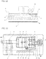
- FIG. 2 is a perspective view showing the power circuit device 1 according to the first embodiment of the invention, wherein the system power supply 100 is not shown.
- FIG. 3 is a side view of a rectifier circuit 4, step-up circuit 10, and inverter 5 portion of the power circuit device 1 according to the first embodiment of the invention.
- a grounding capacitor 3 is attached to either end of a common mode coil 2.
- An upper limit value of capacitance of the grounding capacitor 3, taking leakage current into account, is in the region of 4,700 pF.
- One common mode coil 2 is connected to the system power supply 100, while another is connected to the rectifier circuit 4.
- the rectifier circuit 4 is connected to the step-up circuit 10, which is formed of an inductor, a semiconductor element, and a diode.
- the step-up circuit 10 is connected to the inverter 5 via an electrolytic capacitor.
- Positive polarity sides of the rectifier circuit 4, step-up circuit 10, and inverter 5 form a first wire 7, while negative polarity sides thereof form a second wire 8.
- the positive polarity side of the rectifier circuit 4 and the inverter 5 are connected by the first wire 7, while the negative polarity side of the rectifier circuit 4 and the inverter 5 are connected by the second wire 8.
- the load 6 is connected to an output wire 23 and ground wire terminal 22a of the power circuit device 1. Also, an electrical wire of the load 6 is connected to a metal frame 9 via floating capacitance.
- the metal frame 9 is a chassis included in the power circuit device 1, and the load 6 is shown as being mounted on top of the metal frame 9 in FIG. 1 , but this is shown in order to express an electrical connection relationship with the load 6, and differs from an actual structure.
- a ground wire 22 is connected to a conductive plate 21, and the rectifier circuit 4 side of the common mode coil 2 and the conductive plate 21 are connected by a bypass capacitor 20 connected farther to the system power supply 100 side than the rectifier circuit 4.
- a noise loop 15 is formed from the rectifier circuit 4 by the first wire 7, including the step-up circuit 10, the inverter 5, output wire 23, load 6, ground wire terminal 22a, ground wire 22, conductive plate 21, and bypass capacitor 20.
- a heatsink 30 is provided for heat release in the rectifier circuit 4 and inverter 5, and the heatsink 30 and conductive plate 21 are disposed one on either side surface of a printed circuit board 11 so as to sandwich the printed circuit board 11.
- the heatsink 30 is shown as being a single article in FIG. 1 , a disposition may be such that one heatsink 30 is shared by the rectifier circuit 4 and inverter 5, or there may be individual heatsinks 30 for the rectifier circuit 4 and inverter 5.
- noise flowing from the inverter 5 and step-up circuit 10 into the metal frame 9 via the floating capacitance of the load 6 is led to the conductive plate 21 by the noise loop 15, whereby the flow to the metal frame 9 can be reduced. Because of this, noise flowing from the load 6 into the metal frame 9 is restricted, and the amount of noise propagating to the system power supply 100 can be restricted.
- the noise loop 15 can be formed even when using a part with height, such as an electrolytic capacitor, and disposing the rectifier circuit 4 and inverter 5 on the same side as the electrolytic capacitor.
- the noise loop 15 is formed of the inverter 5, an electrical wire connecting the inverter and load 6, the load 6, the floating capacitance of the load 6, the ground wire 22, the conductive plate 21, the bypass capacitor 20, the rectifier circuit 4, the step-up circuit 10, and the inverter 5.
- a loop that passes along the first wire 7 is shown in FIG. 1
- the noise loop may be a loop that passes along the second wire 8.
- the noise loop 15, which can lead noise flowing from the inverter 5 and step-up circuit 10 into the metal frame 9 via the floating capacitance of the load 6, is provided when attempting to increase an amount of attenuation by a noise filter formed of the common mode coil 2 and grounding capacitor 3 by providing the grounding capacitor 3 at either end of the common mode coil 2, because of which the amount of noise flowing into the metal frame 9 via the floating capacitance of the load 6 that propagates to the system power supply 100 can be restricted.
- FIG. 1 A diagram of a state wherein the power circuit device 1 is enclosed by the metal frame 9 is shown in FIG. 1 , but the metal frame 9 may be simply installed below the power circuit device 1, rather than enclosing the power circuit device 1.
- the ground wire 22 may be a shield of a shielded wire that links the power circuit device 1 and load 6.
- the noise loop 15, which can collect noise flowing from the inverter 5 and step-up circuit 10 into the metal frame 9 via the floating capacitance of the load 6, is formed, and not only can the amount of noise flowing into the metal frame 9 via the floating capacitance of the load 6 that propagates to the system power supply 100 be restricted, but also noise radiating from a cable connecting the output wire 23 and load 6 can also be restricted.
- a configuration may be such that the conductive plate 21 is configured of a first conductive plate 21a, disposed on the same side as the heatsink 30 with respect to the printed circuit board 11, and a second conductive plate 21b, disposed on the opposite side to the heatsink 30 with respect to the printed circuit board 11, and the first conductive plate 21a and second conductive plate 21b are connected by a via hole 31, as shown in FIG. 4 and FIG. 5 .
- the noise loop 15 can be formed even when using a part with height, such as an electrolytic capacitor, and disposing the rectifier circuit 4 and inverter 5 on the side of the printed circuit board 11 opposite the surface on which the electrolytic capacitor is provided.
- a sandwich structure wherein the first wire 7 and second wire 8 are disposed so as to sandwich the conductive plate 21 from either side, as in FIG. 6 , may be adopted.
- the positive polarity side of the rectifier circuit 4 and the first wire 7 are connected
- the negative polarity side of the rectifier circuit 4 and the second wire 8 are connected
- the positive polarity side of the inverter 5 and the first wire 7 are connected
- the negative polarity side of the inverter 5 and the second wire 8 are connected.
- the positive polarity side of the electrolytic capacitor and the first wire 7 are connected
- the negative polarity side of the electrolytic capacitor and the second wire 8 are connected.
- the noise loop 15 is configured of the inverter 5, an electrical wire connecting the inverter 5 and load 6, the load 6, the floating capacitance of the load 6, the ground wire terminal 22a, the ground wire 22, the conductive plate 21, the bypass capacitor 20, the rectifier circuit 4, the step-up circuit 10, and the inverter 5.
- inductance of the noise loop 15 can be further reduced in comparison with that in the first and second embodiments, because of which collection of noise flowing from the inverter 5 and step-up circuit 10 into the metal frame 9 via the floating capacitance of the load 6 can be carried out more efficiently. Because of this, propagation of noise flowing into the metal frame 9 via the floating capacitance of the load 6 can be restricted, and the amount of noise propagating to the system power supply 100 can be restricted.
- the heatsink 30 may be grounded with the metal frame 9, as in FIG. 7 .
- Grounding of the heatsink 30 with the metal frame 9 is desirably carried out in one place in the vicinity of a place in which the load 6 and metal frame 9 are in contact.
- grounding of the heatsink 30 with the conductive plate 21 can be realized by fixing with a metal screw, fixture, or the like, from the conductive plate 21 through the rectifier circuit 4 or inverter 5 to the heatsink 30.
- the noise loop 15 can be formed of the inverter 5, an electrical wire connecting the inverter 5 and load 6, the load 6, the floating capacitance of the load 6, the ground wire terminal 22a, the ground wire 22, the conductive plate 21, the bypass capacitor 20, the rectifier circuit 4, the step-up circuit 10, and the inverter 5, even when the heatsink 30 is grounded with the metal frame 9.
- the noise loop 15 of this aspect too is such that, in the same way as in the other embodiments, noise flowing from the inverter 5 and step-up circuit 10 into the metal frame 9 via the floating capacitance of the load 6 can be led, and the amount of noise flowing into the metal frame 9 via the floating capacitance of the load 6 that propagates to the system power supply 100 can be restricted.
- FIG. 8 is a circuit diagram showing the power circuit device 1 according to a fifth embodiment of the invention.
- FIG. 9 is a perspective view showing the power circuit device 1 according to the fifth embodiment of the invention.
- the grounding capacitor 3 is disposed at either end of the common mode coil 2 in the power circuit device 1, one side of the common mode coil 2 is connected to the system power supply 100, and the other is connected to the rectifier circuit 4.
- the rectifier circuit 4 is connected to the step-up circuit 10.
- the step-up circuit 10 is connected to the inverter 5 via an electrolytic capacitor, the positive polarity sides of the rectifier circuit 4, step-up circuit 10, and inverter 5 form the first wire 7, and the negative polarity sides thereof form the second wire 8.
- the inverter 5 is connected to the load 6, and an electrical wire of the load 6 is connected to the metal frame 9 via the floating capacitance.
- the load 6 is connected to the conductive plate 21 via the ground wire terminal 22a, and the inverter 5 side of the step-up circuit 10 and the conductive plate 21 are connected by the bypass capacitor 20.
- the heatsink 30 is provided for heat release of the rectifier circuit 4 and inverter 5, and the heatsink 30 and conductive plate 21 are disposed on a surface of the printed circuit board 11 differing from that on which the rectifier circuit 4 and inverter 5 are disposed.
- noise flowing from the inverter 5 and step-up circuit 10 to the metal frame 9 via the floating capacitance of the load 6 is unlikely to flow into the metal frame 9 owing to the noise loop 15, and the amount of noise flowing into the metal frame from the load connected via the inverter and electrical wire that propagates to the system power supply can be restricted.
- the noise loop 15 can be formed even when using a part with height, such as an electrolytic capacitor, and disposing the rectifier circuit 4 and inverter 5 on the same side as the electrolytic capacitor.
- the noise loop 15 is formed of the inverter 5, an electrical wire connecting the inverter 5 and load 6, the load 6, the floating capacitance of the load 6, the ground wire terminal 22a, the ground wire 22, the conductive plate 21, the bypass capacitor 20, and the inverter 5. Although a loop that passes along the first wire 7 is shown in FIG. 8 , the noise loop may be a loop that passes along the second wire 8.
- the noise loop 15, which can lead noise flowing from the step-up circuit 10 and inverter 5 into the metal frame 9 via the floating capacitance of the load 6, is provided when attempting to increase the amount of attenuation by providing the grounding capacitor 3 at either end of the common mode coil 2, because of which propagation of noise flowing into the metal frame 9 via the floating capacitance of the load 6 can be restricted, and the amount of noise propagating to the system power supply 100 can be restricted.
- the ground wire 22 may be a shield of a shielded wire that links the power circuit device 1 and load 6.
- the noise loop 15, which can lead noise flowing from the inverter 5 and step-up circuit 10 into the metal frame 9 via the floating capacitance of the load 6, is formed, and not only can the amount of noise flowing into the metal frame 9 via the floating capacitance of the load 6 that propagates to the system power supply 100 be restricted, but also noise radiating from a cable connecting the output wire 23 and load 6 can also be restricted.
- FIG. 8 a diagram wherein the power circuit device 1 is enclosed by the metal frame 9 is shown in FIG. 8 , but the metal frame 9 may be simply installed below the power circuit device 1, rather than enclosing the power circuit device 1.
- bypass capacitor 20 is connected farther to the system power supply 100 side than the rectifier circuit 4 has been described in the second embodiment, but a case wherein the inverter 5 side of the step-up circuit 10 and the conductive plate 21 are connected by the bypass capacitor 20 can be implemented as follows.
- the noise loop 15 can be formed even when using a part with height, such as an electrolytic capacitor, and disposing the rectifier circuit 4 and inverter 5 on a surface differing from that of the electrolytic capacitor.
- bypass capacitor 20 is connected farther to the system power supply 100 side than the rectifier circuit 4 has been described in the third embodiment, but a case wherein the inverter 5 side of the step-up circuit 10 and the conductive plate 21 are connected by the bypass capacitor 20 can be implemented as follows.
- a sandwich structure wherein the first wire 7 and second wire 8 are disposed so as to sandwich the conductive plate 21 from either side is adopted, as in FIG. 11 .
- This structure is such that the positive polarity side of the inverter 5 and the first wire 7 are connected, and the negative polarity side of the inverter 5 and the second wire 8 are connected. Furthermore, in the same way, the positive polarity side of the electrolytic capacitor and the first wire 7 are connected, and the negative polarity side of the electrolytic capacitor and the second wire 8 are connected.
- the noise loop 15 is configured of the inverter 5, an electrical wire connecting the inverter 5 and load 6, the load 6, the floating capacitance of the load 6, the ground wire terminal 22a, the ground wire 22, the conductive plate 21, the bypass capacitor 20, and the inverter 5, and inductance of the noise loop 15 can be further reduced in comparison with that in the fifth embodiment and sixth embodiment, because of which noise flowing into the metal frame 9 via the floating capacitance of the load 6 can be led by the noise loop 15, and the amount of noise propagating from the metal frame 9 to the system power supply 100 can be restricted.
- the heatsink 30 may be grounded with the metal frame 9, as in FIG. 12 .
- Grounding of the heatsink 30 with the metal frame 9 is desirably carried out in one place in the vicinity of a place in which the load 6 and metal frame 9 are in contact.
- grounding of the heatsink 30 with the conductive plate 21 can be realized by fixing with a metal screw, fixture, or the like, from the conductive plate 21 through the rectifier circuit 4 or inverter 5 to the heatsink.
- the noise loop 15 formed of the inverter 5, an electrical wire connecting the inverter and load, the load 6, the floating capacitance of the load 6, the ground wire 22, the conductive plate 21, the bypass capacitor 20, and the inverter 5 can be formed, noise flowing from the inverter 5 and step-up circuit 10 into the metal frame 9 via the floating capacitance of the load 6 can be led by the noise loop 15, propagation of noise flowing into the metal frame 9 is restricted, and the amount of noise propagating to the system power supply 100 can be restricted.
- FIG. 13 is a circuit diagram showing the power circuit device 1 according to the ninth embodiment of the invention.
- the power circuit device 1 is such that the metal frame 9 shown in FIG. 8 is divided into a first metal frame 9a and a second metal frame 9b.
- the first metal frame 9a and second metal frame 9b are not electrically connected, but the second metal frame 9b is connected to the ground wire terminal 22a.
- noise flowing from the inverter 5 and step-up circuit 10 into the second metal frame 9b via the floating capacitance of the load 6 is unlikely to flow into the first metal frame 9a owing to a noise loop 16, and the amount of noise propagating to the system power supply can be restricted.
- the noise loop 16 is formed of the inverter 5, an electrical wire connecting the inverter 5 and load 6, the load 6, the floating capacitance of the load 6, the ground wire terminal 22a, the second metal frame 9b, the ground wire 22, the conductive plate 21, the bypass capacitor 20, and the inverter 5.
- the noise loop 16 may be a loop that passes along the second wire 8.
- the bypass capacitor 20 may be disposed on the inverter 5 side of the rectifier circuit 4, in which case the noise loop 16 is formed of the inverter 5, an electrical wire connecting the inverter 5 and load 6, the load 6, the floating capacitance of the load 6, the ground wire terminal 22a, the second metal frame 9b, the ground wire 22, the conductive plate 21, the bypass capacitor 20, and the inverter 5.
- the noise loop 16 which can lead noise flowing from the step-up circuit 10 and inverter 5 into the metal frame 9 via the floating capacitance of the load 6, is provided when attempting to increase an amount of attenuation by providing the grounding capacitor 3 at either end of the common mode coil 2, because of which propagation of noise flowing into the first metal frame 9a and system power supply 100 via the floating capacitance of the load 6, the ground wire terminal 22a, the second metal frame 9b, the ground wire 22, and the conductive plate 21 can be restricted, and the amount of noise propagating to the system power supply 100 can be restricted.
- the ground wire 22 may be a shield of a shielded wire that links the power circuit device 1 and load 6.
- the noise loop 16 which can lead noise flowing from the inverter 5 and step-up circuit 10 into the second metal frame 9b via the floating capacitance of the load 6, is formed, and not only can the amount of noise flowing into the second metal frame 9b via the floating capacitance of the load 6 that propagates to the system power supply 100 be restricted, but also noise radiating from a cable connecting the inverter 5 and load 6 can also be restricted.
- FIG. 13 a diagram wherein the first metal frame 9a and second metal frame 9b are installed below the power circuit device 1 is shown in FIG. 13 , but the first metal frame 9a and second metal frame 9b may enclose the power circuit device 1.
- the heatsink 30 may be grounded with the first metal frame 9a or second metal frame 9b.
- Grounding of the heatsink 30 with the first metal frame 9a or second metal frame 9b is desirably carried out in one place in the vicinity of a place in which the load 6 and first metal frame 9a or second metal frame 9b are in contact.
- grounding of the heatsink 30 with the conductive plate 21 can be realized by fixing with a metal screw, fixture, or the like, from the conductive plate 21 through the rectifier circuit 4 or inverter 5 to the heatsink 30.
- FIG. 13 A case wherein the first metal frame 9a and second metal frame 9b are not electrically connected is shown in FIG. 13 , but the conductive plate 21 and first metal frame 9a may be connected by an inductor 32, and the conductive plate 21 and second metal frame 9b connected by the ground wire 22, as in FIG. 14 .
- a value of the inductor 32 is determined so that impedance of a noise loop 17 is higher than that of the noise loop 16.
- the noise loop 16 is formed of the inverter 5, an electrical wire connecting the inverter 5 and load 6, the load 6, the floating capacitance of the load 6, the ground wire terminal 22a, the second metal frame 9b, the ground wire 22, the conductive plate 21, the bypass capacitor 20, and the inverter 5.
- the noise loop 17 is formed of the inverter 5, an electrical wire connecting the inverter 5 and load 6, the load 6, the floating capacitance of the load 6, the ground wire terminal 22a, the second metal frame 9b, the ground wire 22, the conductive plate 21, the inductor 32, the first metal frame 9a, the grounding capacitor 3, the rectifier circuit 4, and the inverter 5.
- the noise loop may be a loop that passes along the second wire 8.
- the bypass capacitor 20 may be disposed on the inverter 5 side of the rectifier circuit 4, in which case the noise loop 16 is formed of the inverter 5, an electrical wire connecting the inverter 5 and load 6, the load 6, the floating capacitance of the load 6, the ground wire terminal 22a, the second metal frame 9b, the ground wire 22, the conductive plate 21, the bypass capacitor 20, and the inverter 5.
- the noise loop 16 which can lead noise flowing from the step-up circuit 10 and inverter 5 into the second metal frame 9b via the floating capacitance of the load 6, is provided when attempting to increase an amount of attenuation by providing the grounding capacitor 3 at either end of the common mode coil 2, because of which propagation of noise flowing into the first metal frame 9a and system power supply 100 via the floating capacitance of the load 6, the ground wire terminal 22a, the second metal frame 9b, the ground wire 22, and the conductive plate 21 can be restricted, and the amount of noise propagating to the system power supply 100 can be restricted.
- ground wire 22 may be a shield of a shielded wire that links the power circuit device 1 and load 6.
- the noise loop 16 which can lead noise flowing from the inverter 5 and step-up circuit 10 into the second metal frame 9b via the floating capacitance of the load 6, is formed, and not only can the amount of noise flowing into the second metal frame 9b via the floating capacitance of the load 6 that propagates to the system power supply 100 be restricted, but also noise radiating from a cable connecting the inverter 5 and load 6 can also be restricted.
- FIG. 14 a diagram wherein the first metal frame 9a and second metal frame 9b are installed below the power circuit device 1 is shown in FIG. 14 , but the first metal frame 9a and second metal frame 9b may enclose the power circuit device 1.
- the heatsink 30 may be grounded with the first metal frame 9a or second metal frame 9b.
- Grounding of the heatsink 30 with the first metal frame 9a or second metal frame 9b is desirably carried out in one place in the vicinity of a place in which the load 6 and first metal frame 9a or second metal frame 9b are in contact.
- grounding of the heatsink 30 with the conductive plate 21 can be realized by fixing with a metal screw, fixture, or the like, from the conductive plate 21 through the rectifier circuit 4 or inverter 5 to the heatsink 30.
- FIG. 13 A case wherein the first metal frame 9a and second metal frame 9b are not electrically connected is shown in FIG. 13 , but the conductive plate 21 and first metal frame 9a may be connected by resistor 33, and the conductive plate 21 and second metal frame 9b connected by the ground wire 22, as in FIG. 15 .
- a value of the resistor 33 is determined so that impedance of the noise loop 17 is higher than that of the noise loop 16, as shown in FIG. 14 in the tenth embodiment.
- FIG. 16 is a circuit diagram showing the power circuit device 1 according to the twelfth embodiment of the invention.
- the conductive plate 21 and first metal frame 9a are connected by a first inductor 34
- the conductive plate 21 and second metal frame 9b are connected by the ground wire 22, and furthermore, the first metal frame 9a and second metal frame 9b are connected by a second inductor 35.
- the bypass capacitor 20 may be disposed on the inverter 5 side of the rectifier circuit 4.
- the power circuit device 1 being configured in this way, the amount of propagation of noise flowing from the step-up circuit 10 and inverter 5 via the floating capacitance of the load 6, the ground wire terminal 22a, the second metal frame 9b, the ground wire 22, and the conductive plate 21, or from the step-up circuit 10 and inverter 5 via the floating capacitance of the load 6, the ground wire terminal 22a, the second metal frame 9b, and the second inductor 35, into the first metal frame 9a and system power supply 100 can be restricted when attempting to increase the amount of attenuation by providing the grounding capacitor 3 at either end of the common mode coil 2.
- the ground wire 22 may be a shield of a shielded wire that links the power circuit device 1 and load 6.
- the noise loop 16 which can lead noise flowing from the inverter 5 and step-up circuit 10 into the second metal frame 9b via the floating capacitance of the load 6, is formed, and not only can the amount of noise flowing into the second metal frame 9b via the floating capacitance of the load 6 that propagates to the system power supply 100 be restricted, but also noise radiating from a cable connecting the inverter 5 and load 6 can also be restricted.
- FIG. 16 a diagram wherein the first metal frame 9a and second metal frame 9b are installed below the power circuit device 1 is shown in FIG. 16 , but the first metal frame 9a and second metal frame 9b may enclose the power circuit device 1.
- the heatsink 30 may be grounded with the first metal frame 9a or second metal frame 9b.
- Grounding of the heatsink 30 with the first metal frame 9a or second metal frame 9b is desirably carried out in one place in the vicinity of a place in which the load 6 and first metal frame 9a or second metal frame 9b are in contact.
- grounding of the heatsink 30 with the conductive plate 21 can be realized by fixing with a metal screw, fixture, or the like, from the conductive plate 21 through the rectifier circuit 4 or inverter 5 to the heatsink 30.
- FIG. 16 A case wherein the conductive plate 21 and first metal frame 9a are connected by the first inductor 34 is shown in FIG. 16 , but the conductive plate 21 and first metal frame 9a may be connected by the resistor 33, the first metal frame 9a and second metal frame 9b connected by an inductor, and the conductive plate 21 and second metal frame 9b connected by the ground wire 22, as in FIG. 17 .
- the power circuit device 1 being configured in this way, the amount of propagation of noise flowing from the step-up circuit 10 and inverter 5 via the floating capacitance of the load 6, the ground wire terminal 22a, the second metal frame 9b, the ground wire 22, and the conductive plate 21, or from the step-up circuit 10 and inverter 5 via the floating capacitance of the load 6, the ground wire terminal 22a, the second metal frame 9b, and an inductor 36, into the first metal frame 9a and system power supply 100 can be restricted when attempting to increase the amount of attenuation by providing the grounding capacitor 3 at either end of the common mode coil 2.
- first metal frame 9a and second metal frame 9b are connected by the second inductor 35 is shown in FIG. 16 , but the conductive plate 21 and first metal frame 9a may be connected by the inductor 32, the first metal frame 9a and second metal frame 9b connected by resistor 37, and the conductive plate 21 and second metal frame 9b connected by the ground wire 22, as in FIG. 18 .
- the power circuit device 1 being configured in this way, the amount of propagation of noise flowing from the step-up circuit 10 and inverter 5 via the floating capacitance of the load 6, the ground wire terminal 22a, the second metal frame 9b, the ground wire 22, and the conductive plate 21, or from the step-up circuit 10 and inverter 5 via the floating capacitance of the load 6, the ground wire terminal 22a, the second metal frame 9b, and the resistor 37, into the first metal frame 9a and system power supply 100 can be restricted when attempting to increase the amount of attenuation by providing the grounding capacitor 3 at either end of the common mode coil 2.
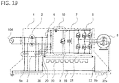
- first metal frame 9a and second metal frame 9b are connected by the second inductor 35 and the conductive plate 21 and first metal frame 9a are connected by the first inductor 34 is shown in FIG. 16 , but the conductive plate 21 and first metal frame 9a may be connected by a first resistor 38, the first metal frame 9a and second metal frame 9b connected by a second resistor 39, and the conductive plate 21 and second metal frame 9b connected by the ground wire 22, as in FIG. 19 .
- the power circuit device 1 being configured in this way, the amount of propagation of noise flowing from the step-up circuit 10 and inverter 5 via the floating capacitance of the load 6, the ground wire terminal 22a, the second metal frame 9b, the ground wire 22, and the conductive plate 21, or from the step-up circuit 10 and inverter 5 via the floating capacitance of the load 6, the ground wire terminal 22a, the second metal frame 9b, and the second resistor 39, into the first metal frame 9a and system power supply 100 can be restricted when attempting to increase the amount of attenuation by providing the grounding capacitor 3 at either end of the common mode coil 2.
Landscapes
- Engineering & Computer Science (AREA)
- Power Engineering (AREA)
- Physics & Mathematics (AREA)
- Electromagnetism (AREA)
- Microelectronics & Electronic Packaging (AREA)
- Inverter Devices (AREA)
- Rectifiers (AREA)
Abstract
Description
- The present invention relates to a power circuit device including an inverter that converts alternating current input from a system power supply into direct current, and subsequently into alternating current again.
- Generally, electronic equipment generates electrical noise, and equipment for which a countermeasure is insufficient is a factor in causing various problems. In particular, an electrical equipment that operates on an alternating current power supply is often connected via a shared power supply line, and may experience a malfunction due to noise generated in another electrical equipment, or conversely, cause another device to malfunction due to noise generated in a device of the equipment itself.
- As a source of noise, there can be a slight electrical discharge in an electrical switch and various kinds of motor caused by a semiconductor such as an inverter, and the like, and weakening of energy generated in the source of noise, and causing transmission in a noise transmission path to be difficult, are carried out as noise countermeasures.
- Noise propagation is divided into two kinds depending on a transmission method thereof, wherein the first is normal mode noise generated between signal lines and between power supply lines, and is a noise component that is generated between power supply paths and flows in the same direction as a power supply current or signal.
- As noise current directions in the normal mode are of opposite orientations when going and returning, noise components are cancelled out and decrease, because of which there is little radiation noise, and this noise is countered by using filters in signal lines and power supply lines. The second is common mode noise generated between a signal line or power supply line and a ground, and this noise flows in the same direction to a signal pattern and SG (signal ground), passes through a metal frame, and returns to a signal source through a floating capacitance or the like.
- Noise in the common mode is such that a large power supply loop is formed, which is important as a noise countermeasure as a large noise is radiated with even a small noise current. In response to this noise, filters are used between positive and negative signal lines and positive and negative power supply lines.
-
Patent Document 1 proposes a power circuit device that converts alternating current input from a system power supply into direct current, and subsequently into alternating current again, wherein, as a countermeasure for common mode noise, particularly in order to restrict radiation noise, a conductive plate is provided so that a common mode noise current is not caused to flow directly into a metal frame, the conductive plate and a bypass capacitor of a circuit configuring a power supply circuit are connected, and by the common mode noise current being taken in and connected to one point on the metal frame via an inductor, radiation noise is prevented from exiting directly from the metal frame. - Also,
Patent Document 2 proposes using impedance elements to connect first and second radiators provided respectively in a first converter that converts alternating current into direct current and a second converter that converts direct current into alternating current, and reducing a wave height value of a common mode noise current by arranging that the common mode noise current always flows through the impedance elements. -
- Patent Document 1:
-
JP-A-2000-341951 - Patent Document 2:
-
JP-A-2006-115649 - A switching power supply device shown in
Patent Document 1 is such that, even when attempting to increase an amount of attenuation by including a grounding capacitor at either end (a rectifier circuit side and a system power supply side) of a common mode coil in response to a common mode noise current flowing into a metal frame from a load connected via an inverter and electrical wire, a noise transmission path is formed of a rectifier circuit, the rectifier circuit side grounding capacitor of the grounding capacitors, a conductive plate, the system power supply side grounding capacitor of the grounding capacitors, a system power supply, a ground, a metal frame, a floating capacitance between the metal frame and conductive plate, a bypass capacitor, and the rectifier circuit, without passing through the common mode coil, and there is a problem in that the advantage of attenuating the amount of noise propagating is not as expected. - Also, a power conversion device shown in
Patent Document 2 is such that causing noise to flow into a radiator for cooling a semiconductor module without causing noise to flow into a metal frame is proposed, but when a radiator is used, a new propagation path is formed due to a semiconductor module connected to the radiator and parasitic capacitance of the radiator, and the noise propagation path becomes complex, because of which there is a problem in that attenuating noise is difficult. - The invention, having been contrived in order to resolve the heretofore described kinds of problem, has an object of providing a power circuit device such that the amount of noise flowing into a metal frame from a load that propagates to a system power supply can be restricted, even when a grounding capacitor is included at either end of a common mode coil.
- A power circuit device according to the invention includes a rectifier circuit, an inverter, a first electrical wire that connects a positive polarity side of the rectifier circuit and the inverter, a second electrical wire that connects a negative polarity side of the rectifier circuit and the inverter, a ground terminal that can connect a load connected to an output terminal of the inverter, and a conductive plate that connects at least one of the first electrical wire and second electrical wire and the ground wire terminal.
- According to the invention, at least one of a first electrical wire, which connects a positive polarity side of a rectifier circuit and an inverter, and a second electrical wire, which connects a negative polarity side of the rectifier circuit and the inverter, and a ground wire terminal are connected by a conductive plate, thereby forming a loop that can collect noise flowing out from a load, noise propagating from the load propagates to the conductive plate through the ground wire terminal, and noise flowing from the load into a system power supply can be restricted.
-
- FIG. 1
- is a circuit diagram of a power circuit device according to a first embodiment of the invention.
- FIG. 2
- is a perspective view of the power circuit device according to the first embodiment of the invention.
- FIG. 3
- is a side view of the power circuit device according to the first embodiment of the invention.
- FIG. 4
- is a perspective view of a power circuit device according to a second embodiment of the invention.
- FIG. 5
- is a side view of the power circuit device according to the second embodiment of the invention.
- FIG. 6
- is a side view of a power circuit device according to a third embodiment of the invention.
- FIG. 7
- is a circuit diagram of a power circuit device according to a fourth embodiment of the invention.
- FIG. 8
- is a circuit diagram of a power circuit device according to a fifth embodiment of the invention.
- FIG. 9
- is a perspective view of the power circuit device according to the fifth embodiment of the invention.
- FIG. 10
- is a perspective view of a power circuit device according to a sixth embodiment of the invention.
- FIG. 11
- is a side view of a power circuit device according to a seventh embodiment of the invention.
- FIG. 12
- is a circuit diagram of a power circuit device according to an eighth embodiment of the invention.
- FIG. 13
- is a circuit diagram of a power circuit device according to a ninth embodiment of the invention.
- FIG. 14
- is a circuit diagram of a power circuit device according to a tenth embodiment of the invention.
- FIG. 15
- is a circuit diagram of a power circuit device according to an eleventh embodiment of the invention.
- FIG. 16
- is a circuit diagram of a power circuit device according to a twelfth embodiment of the invention.
- FIG. 17
- is a circuit diagram of a power circuit device according to a thirteenth embodiment of the invention.
- FIG. 18
- is a circuit diagram of a power circuit device according to a fourteenth embodiment of the invention.
- FIG. 19
- is a circuit diagram of a power circuit device according to a fifteenth embodiment of the invention.
- Hereafter, a first embodiment of the invention will be described.
-
FIG. 1 is a circuit diagram showing apower circuit device 1 according to the first embodiment of the invention, wherein asystem power supply 100 andload 6 connected to thepower circuit device 1 are included inFIG. 1. FIG. 2 is a perspective view showing thepower circuit device 1 according to the first embodiment of the invention, wherein thesystem power supply 100 is not shown.FIG. 3 is a side view of arectifier circuit 4, step-upcircuit 10, andinverter 5 portion of thepower circuit device 1 according to the first embodiment of the invention. - As shown in
FIG. 1 , agrounding capacitor 3 is attached to either end of acommon mode coil 2. An upper limit value of capacitance of thegrounding capacitor 3, taking leakage current into account, is in the region of 4,700 pF. Onecommon mode coil 2 is connected to thesystem power supply 100, while another is connected to therectifier circuit 4. Therectifier circuit 4 is connected to the step-upcircuit 10, which is formed of an inductor, a semiconductor element, and a diode.
The step-upcircuit 10 is connected to theinverter 5 via an electrolytic capacitor. Positive polarity sides of therectifier circuit 4, step-upcircuit 10, andinverter 5 form afirst wire 7, while negative polarity sides thereof form asecond wire 8. In other words, the positive polarity side of therectifier circuit 4 and theinverter 5 are connected by thefirst wire 7, while the negative polarity side of therectifier circuit 4 and theinverter 5 are connected by thesecond wire 8. - Also, the
load 6 is connected to anoutput wire 23 andground wire terminal 22a of thepower circuit device 1. Also, an electrical wire of theload 6 is connected to ametal frame 9 via floating capacitance. Themetal frame 9 is a chassis included in thepower circuit device 1, and theload 6 is shown as being mounted on top of themetal frame 9 inFIG. 1 , but this is shown in order to express an electrical connection relationship with theload 6, and differs from an actual structure. - A
ground wire 22 is connected to aconductive plate 21, and therectifier circuit 4 side of thecommon mode coil 2 and theconductive plate 21 are connected by abypass capacitor 20 connected farther to thesystem power supply 100 side than therectifier circuit 4. - According to this configuration, a
noise loop 15 is formed from therectifier circuit 4 by thefirst wire 7, including the step-upcircuit 10, theinverter 5,output wire 23,load 6,ground wire terminal 22a,ground wire 22,conductive plate 21, andbypass capacitor 20. - A
heatsink 30 is provided for heat release in therectifier circuit 4 andinverter 5, and theheatsink 30 andconductive plate 21 are disposed one on either side surface of a printedcircuit board 11 so as to sandwich the printedcircuit board 11. Although theheatsink 30 is shown as being a single article inFIG. 1 , a disposition may be such that oneheatsink 30 is shared by therectifier circuit 4 andinverter 5, or there may beindividual heatsinks 30 for therectifier circuit 4 andinverter 5. - According to this kind of configuration, noise flowing from the
inverter 5 and step-upcircuit 10 into themetal frame 9 via the floating capacitance of theload 6 is led to theconductive plate 21 by thenoise loop 15, whereby the flow to themetal frame 9 can be reduced. Because of this, noise flowing from theload 6 into themetal frame 9 is restricted, and the amount of noise propagating to thesystem power supply 100 can be restricted. Thenoise loop 15 can be formed even when using a part with height, such as an electrolytic capacitor, and disposing therectifier circuit 4 andinverter 5 on the same side as the electrolytic capacitor. - The
noise loop 15 is formed of theinverter 5, an electrical wire connecting the inverter andload 6, theload 6, the floating capacitance of theload 6, theground wire 22, theconductive plate 21, thebypass capacitor 20, therectifier circuit 4, the step-upcircuit 10, and theinverter 5. Although a loop that passes along thefirst wire 7 is shown inFIG. 1 , the noise loop may be a loop that passes along thesecond wire 8. - By the
power circuit device 1 being configured in this way, thenoise loop 15, which can lead noise flowing from theinverter 5 and step-upcircuit 10 into themetal frame 9 via the floating capacitance of theload 6, is provided when attempting to increase an amount of attenuation by a noise filter formed of thecommon mode coil 2 andgrounding capacitor 3 by providing thegrounding capacitor 3 at either end of thecommon mode coil 2, because of which the amount of noise flowing into themetal frame 9 via the floating capacitance of theload 6 that propagates to thesystem power supply 100 can be restricted. - A diagram of a state wherein the
power circuit device 1 is enclosed by themetal frame 9 is shown inFIG. 1 , but themetal frame 9 may be simply installed below thepower circuit device 1, rather than enclosing thepower circuit device 1. - Also, the
ground wire 22 may be a shield of a shielded wire that links thepower circuit device 1 andload 6. According to this configuration, thenoise loop 15, which can collect noise flowing from theinverter 5 and step-upcircuit 10 into themetal frame 9 via the floating capacitance of theload 6, is formed, and not only can the amount of noise flowing into themetal frame 9 via the floating capacitance of theload 6 that propagates to thesystem power supply 100 be restricted, but also noise radiating from a cable connecting theoutput wire 23 andload 6 can also be restricted. - Also, when using a part with height, such as an electrolytic capacitor, and disposing the
rectifier circuit 4 andinverter 5 on a back surface side of the printedcircuit board 11, that is, on the side opposite the surface on which the electrolytic capacitor is provided, a configuration may be such that theconductive plate 21 is configured of a firstconductive plate 21a, disposed on the same side as theheatsink 30 with respect to the printedcircuit board 11, and a secondconductive plate 21b, disposed on the opposite side to theheatsink 30 with respect to the printedcircuit board 11, and the firstconductive plate 21a and secondconductive plate 21b are connected by a viahole 31, as shown inFIG. 4 andFIG. 5 . - According to this configuration, the
noise loop 15 can be formed even when using a part with height, such as an electrolytic capacitor, and disposing therectifier circuit 4 andinverter 5 on the side of the printedcircuit board 11 opposite the surface on which the electrolytic capacitor is provided. - Also, a sandwich structure wherein the
first wire 7 andsecond wire 8 are disposed so as to sandwich theconductive plate 21 from either side, as inFIG. 6 , may be adopted. In this case too, the positive polarity side of therectifier circuit 4 and thefirst wire 7 are connected, the negative polarity side of therectifier circuit 4 and thesecond wire 8 are connected, the positive polarity side of theinverter 5 and thefirst wire 7 are connected, and the negative polarity side of theinverter 5 and thesecond wire 8 are connected. Furthermore, in the same way, the positive polarity side of the electrolytic capacitor and thefirst wire 7 are connected, and the negative polarity side of the electrolytic capacitor and thesecond wire 8 are connected. - According to this configuration, the
noise loop 15 is configured of theinverter 5, an electrical wire connecting theinverter 5 andload 6, theload 6, the floating capacitance of theload 6, theground wire terminal 22a, theground wire 22, theconductive plate 21, thebypass capacitor 20, therectifier circuit 4, the step-upcircuit 10, and theinverter 5. In the third embodiment, inductance of thenoise loop 15 can be further reduced in comparison with that in the first and second embodiments, because of which collection of noise flowing from theinverter 5 and step-upcircuit 10 into themetal frame 9 via the floating capacitance of theload 6 can be carried out more efficiently. Because of this, propagation of noise flowing into themetal frame 9 via the floating capacitance of theload 6 can be restricted, and the amount of noise propagating to thesystem power supply 100 can be restricted. - Also, in the first embodiment to third embodiment, a case in which the
heatsink 30 is not grounded with themetal frame 9 is shown, but theheatsink 30 may be grounded with themetal frame 9, as inFIG. 7 . Grounding of theheatsink 30 with themetal frame 9 is desirably carried out in one place in the vicinity of a place in which theload 6 andmetal frame 9 are in contact. Also, grounding of theheatsink 30 with theconductive plate 21 can be realized by fixing with a metal screw, fixture, or the like, from theconductive plate 21 through therectifier circuit 4 orinverter 5 to theheatsink 30. - According to this configuration, the
noise loop 15 can be formed of theinverter 5, an electrical wire connecting theinverter 5 andload 6, theload 6, the floating capacitance of theload 6, theground wire terminal 22a, theground wire 22, theconductive plate 21, thebypass capacitor 20, therectifier circuit 4, the step-upcircuit 10, and theinverter 5, even when theheatsink 30 is grounded with themetal frame 9. Thenoise loop 15 of this aspect too is such that, in the same way as in the other embodiments, noise flowing from theinverter 5 and step-upcircuit 10 into themetal frame 9 via the floating capacitance of theload 6 can be led, and the amount of noise flowing into themetal frame 9 via the floating capacitance of theload 6 that propagates to thesystem power supply 100 can be restricted. -
FIG. 8 is a circuit diagram showing thepower circuit device 1 according to a fifth embodiment of the invention.FIG. 9 is a perspective view showing thepower circuit device 1 according to the fifth embodiment of the invention. As shown inFIG. 8 andFIG. 9 , thegrounding capacitor 3 is disposed at either end of thecommon mode coil 2 in thepower circuit device 1, one side of thecommon mode coil 2 is connected to thesystem power supply 100, and the other is connected to therectifier circuit 4. Therectifier circuit 4 is connected to the step-upcircuit 10. - The step-up
circuit 10 is connected to theinverter 5 via an electrolytic capacitor, the positive polarity sides of therectifier circuit 4, step-upcircuit 10, andinverter 5 form thefirst wire 7, and the negative polarity sides thereof form thesecond wire 8. - The
inverter 5 is connected to theload 6, and an electrical wire of theload 6 is connected to themetal frame 9 via the floating capacitance. Theload 6 is connected to theconductive plate 21 via theground wire terminal 22a, and theinverter 5 side of the step-upcircuit 10 and theconductive plate 21 are connected by thebypass capacitor 20. - The
heatsink 30 is provided for heat release of therectifier circuit 4 andinverter 5, and theheatsink 30 andconductive plate 21 are disposed on a surface of the printedcircuit board 11 differing from that on which therectifier circuit 4 andinverter 5 are disposed. - According to this kind of configuration, noise flowing from the
inverter 5 and step-upcircuit 10 to themetal frame 9 via the floating capacitance of theload 6 is unlikely to flow into themetal frame 9 owing to thenoise loop 15, and the amount of noise flowing into the metal frame from the load connected via the inverter and electrical wire that propagates to the system power supply can be restricted. Thenoise loop 15 can be formed even when using a part with height, such as an electrolytic capacitor, and disposing therectifier circuit 4 andinverter 5 on the same side as the electrolytic capacitor. - The
noise loop 15 is formed of theinverter 5, an electrical wire connecting theinverter 5 andload 6, theload 6, the floating capacitance of theload 6, theground wire terminal 22a, theground wire 22, theconductive plate 21, thebypass capacitor 20, and theinverter 5. Although a loop that passes along thefirst wire 7 is shown inFIG. 8 , the noise loop may be a loop that passes along thesecond wire 8. - By the
power circuit device 1 being configured in this way, thenoise loop 15, which can lead noise flowing from the step-upcircuit 10 andinverter 5 into themetal frame 9 via the floating capacitance of theload 6, is provided when attempting to increase the amount of attenuation by providing thegrounding capacitor 3 at either end of thecommon mode coil 2, because of which propagation of noise flowing into themetal frame 9 via the floating capacitance of theload 6 can be restricted, and the amount of noise propagating to thesystem power supply 100 can be restricted. - The
ground wire 22 may be a shield of a shielded wire that links thepower circuit device 1 andload 6. According to this configuration, thenoise loop 15, which can lead noise flowing from theinverter 5 and step-upcircuit 10 into themetal frame 9 via the floating capacitance of theload 6, is formed, and not only can the amount of noise flowing into themetal frame 9 via the floating capacitance of theload 6 that propagates to thesystem power supply 100 be restricted, but also noise radiating from a cable connecting theoutput wire 23 andload 6 can also be restricted. - Also, a diagram wherein the
power circuit device 1 is enclosed by themetal frame 9 is shown inFIG. 8 , but themetal frame 9 may be simply installed below thepower circuit device 1, rather than enclosing thepower circuit device 1. - Also, a case wherein the
bypass capacitor 20 is connected farther to thesystem power supply 100 side than therectifier circuit 4 has been described in the second embodiment, but a case wherein theinverter 5 side of the step-upcircuit 10 and theconductive plate 21 are connected by thebypass capacitor 20 can be implemented as follows. - That is, when using a part with height, such as an electrolytic capacitor, and disposing the
rectifier circuit 4 andinverter 5 on a surface of the printedcircuit board 11 differing from that of the electrolytic capacitor, a configuration wherein theconductive plate 21 is disposed on the same side as the electrolytic capacitor is adopted, as inFIG. 10 . - According to this configuration, the
noise loop 15 can be formed even when using a part with height, such as an electrolytic capacitor, and disposing therectifier circuit 4 andinverter 5 on a surface differing from that of the electrolytic capacitor. - Also, a case wherein the
bypass capacitor 20 is connected farther to thesystem power supply 100 side than therectifier circuit 4 has been described in the third embodiment, but a case wherein theinverter 5 side of the step-upcircuit 10 and theconductive plate 21 are connected by thebypass capacitor 20 can be implemented as follows. - That is, a sandwich structure wherein the
first wire 7 andsecond wire 8 are disposed so as to sandwich theconductive plate 21 from either side is adopted, as inFIG. 11 . This structure is such that the positive polarity side of theinverter 5 and thefirst wire 7 are connected, and the negative polarity side of theinverter 5 and thesecond wire 8 are connected. Furthermore, in the same way, the positive polarity side of the electrolytic capacitor and thefirst wire 7 are connected, and the negative polarity side of the electrolytic capacitor and thesecond wire 8 are connected. - According to this configuration, the
noise loop 15 is configured of theinverter 5, an electrical wire connecting theinverter 5 andload 6, theload 6, the floating capacitance of theload 6, theground wire terminal 22a, theground wire 22, theconductive plate 21, thebypass capacitor 20, and theinverter 5, and inductance of thenoise loop 15 can be further reduced in comparison with that in the fifth embodiment and sixth embodiment, because of which noise flowing into themetal frame 9 via the floating capacitance of theload 6 can be led by thenoise loop 15, and the amount of noise propagating from themetal frame 9 to thesystem power supply 100 can be restricted. - Also, in the fifth embodiment to seventh embodiment, a case in which the
heatsink 30 is not grounded with themetal frame 9 is shown, but in the same way as that shown inFIG. 7 of the fourth embodiment, theheatsink 30 may be grounded with themetal frame 9, as inFIG. 12 . Grounding of theheatsink 30 with themetal frame 9 is desirably carried out in one place in the vicinity of a place in which theload 6 andmetal frame 9 are in contact. Also, grounding of theheatsink 30 with theconductive plate 21 can be realized by fixing with a metal screw, fixture, or the like, from theconductive plate 21 through therectifier circuit 4 orinverter 5 to the heatsink. - According to this configuration, even when the
heatsink 30 is grounded, thenoise loop 15 formed of theinverter 5, an electrical wire connecting the inverter and load, theload 6, the floating capacitance of theload 6, theground wire 22, theconductive plate 21, thebypass capacitor 20, and theinverter 5 can be formed, noise flowing from theinverter 5 and step-upcircuit 10 into themetal frame 9 via the floating capacitance of theload 6 can be led by thenoise loop 15, propagation of noise flowing into themetal frame 9 is restricted, and the amount of noise propagating to thesystem power supply 100 can be restricted. -
FIG. 13 is a circuit diagram showing thepower circuit device 1 according to the ninth embodiment of the invention. As shown inFIG. 13 , thepower circuit device 1 is such that themetal frame 9 shown inFIG. 8 is divided into afirst metal frame 9a and asecond metal frame 9b. Thefirst metal frame 9a andsecond metal frame 9b are not electrically connected, but thesecond metal frame 9b is connected to theground wire terminal 22a. - According to this kind of configuration, noise flowing from the
inverter 5 and step-upcircuit 10 into thesecond metal frame 9b via the floating capacitance of theload 6 is unlikely to flow into thefirst metal frame 9a owing to anoise loop 16, and the amount of noise propagating to the system power supply can be restricted. - The
noise loop 16 is formed of theinverter 5, an electrical wire connecting theinverter 5 andload 6, theload 6, the floating capacitance of theload 6, theground wire terminal 22a, thesecond metal frame 9b, theground wire 22, theconductive plate 21, thebypass capacitor 20, and theinverter 5. - Although a loop that passes along the
first wire 7 is shown inFIG. 13 , thenoise loop 16 may be a loop that passes along thesecond wire 8. Also, thebypass capacitor 20 may be disposed on theinverter 5 side of therectifier circuit 4, in which case thenoise loop 16 is formed of theinverter 5, an electrical wire connecting theinverter 5 andload 6, theload 6, the floating capacitance of theload 6, theground wire terminal 22a, thesecond metal frame 9b, theground wire 22, theconductive plate 21, thebypass capacitor 20, and theinverter 5. - By the
power circuit device 1 being configured in this way, thenoise loop 16, which can lead noise flowing from the step-upcircuit 10 andinverter 5 into themetal frame 9 via the floating capacitance of theload 6, is provided when attempting to increase an amount of attenuation by providing thegrounding capacitor 3 at either end of thecommon mode coil 2, because of which propagation of noise flowing into thefirst metal frame 9a andsystem power supply 100 via the floating capacitance of theload 6, theground wire terminal 22a, thesecond metal frame 9b, theground wire 22, and theconductive plate 21 can be restricted, and the amount of noise propagating to thesystem power supply 100 can be restricted. - Also, the
ground wire 22 may be a shield of a shielded wire that links thepower circuit device 1 andload 6. According to this configuration, thenoise loop 16, which can lead noise flowing from theinverter 5 and step-upcircuit 10 into thesecond metal frame 9b via the floating capacitance of theload 6, is formed, and not only can the amount of noise flowing into thesecond metal frame 9b via the floating capacitance of theload 6 that propagates to thesystem power supply 100 be restricted, but also noise radiating from a cable connecting theinverter 5 andload 6 can also be restricted. - Also, a diagram wherein the
first metal frame 9a andsecond metal frame 9b are installed below thepower circuit device 1 is shown inFIG. 13 , but thefirst metal frame 9a andsecond metal frame 9b may enclose thepower circuit device 1. - Also, in the ninth embodiment, a case in which the
heatsink 30 is not grounded with themetal frame 9 is shown, but theheatsink 30 may be grounded with thefirst metal frame 9a orsecond metal frame 9b. Grounding of theheatsink 30 with thefirst metal frame 9a orsecond metal frame 9b is desirably carried out in one place in the vicinity of a place in which theload 6 andfirst metal frame 9a orsecond metal frame 9b are in contact. Also, grounding of theheatsink 30 with theconductive plate 21 can be realized by fixing with a metal screw, fixture, or the like, from theconductive plate 21 through therectifier circuit 4 orinverter 5 to theheatsink 30. - A case wherein the
first metal frame 9a andsecond metal frame 9b are not electrically connected is shown inFIG. 13 , but theconductive plate 21 andfirst metal frame 9a may be connected by aninductor 32, and theconductive plate 21 andsecond metal frame 9b connected by theground wire 22, as inFIG. 14 . In this case, a value of theinductor 32 is determined so that impedance of anoise loop 17 is higher than that of thenoise loop 16. - The
noise loop 16 is formed of theinverter 5, an electrical wire connecting theinverter 5 andload 6, theload 6, the floating capacitance of theload 6, theground wire terminal 22a, thesecond metal frame 9b, theground wire 22, theconductive plate 21, thebypass capacitor 20, and theinverter 5. Also, thenoise loop 17 is formed of theinverter 5, an electrical wire connecting theinverter 5 andload 6, theload 6, the floating capacitance of theload 6, theground wire terminal 22a, thesecond metal frame 9b, theground wire 22, theconductive plate 21, theinductor 32, thefirst metal frame 9a, thegrounding capacitor 3, therectifier circuit 4, and theinverter 5. - Although a loop that passes along the
first wire 7 is shown inFIG. 14 , the noise loop may be a loop that passes along thesecond wire 8. Also, thebypass capacitor 20 may be disposed on theinverter 5 side of therectifier circuit 4, in which case thenoise loop 16 is formed of theinverter 5, an electrical wire connecting theinverter 5 andload 6, theload 6, the floating capacitance of theload 6, theground wire terminal 22a, thesecond metal frame 9b, theground wire 22, theconductive plate 21, thebypass capacitor 20, and theinverter 5. - By the
power circuit device 1 being configured in this way, thenoise loop 16, which can lead noise flowing from the step-upcircuit 10 andinverter 5 into thesecond metal frame 9b via the floating capacitance of theload 6, is provided when attempting to increase an amount of attenuation by providing thegrounding capacitor 3 at either end of thecommon mode coil 2, because of which propagation of noise flowing into thefirst metal frame 9a andsystem power supply 100 via the floating capacitance of theload 6, theground wire terminal 22a, thesecond metal frame 9b, theground wire 22, and theconductive plate 21 can be restricted, and the amount of noise propagating to thesystem power supply 100 can be restricted. - Also, the
ground wire 22 may be a shield of a shielded wire that links thepower circuit device 1 andload 6. - According to this configuration, the
noise loop 16, which can lead noise flowing from theinverter 5 and step-upcircuit 10 into thesecond metal frame 9b via the floating capacitance of theload 6, is formed, and not only can the amount of noise flowing into thesecond metal frame 9b via the floating capacitance of theload 6 that propagates to thesystem power supply 100 be restricted, but also noise radiating from a cable connecting theinverter 5 andload 6 can also be restricted. - Also, a diagram wherein the
first metal frame 9a andsecond metal frame 9b are installed below thepower circuit device 1 is shown inFIG. 14 , but thefirst metal frame 9a andsecond metal frame 9b may enclose thepower circuit device 1. - Also, in the tenth embodiment, a case in which the
heatsink 30 is not grounded with themetal frame 9 is shown, but theheatsink 30 may be grounded with thefirst metal frame 9a orsecond metal frame 9b. Grounding of theheatsink 30 with thefirst metal frame 9a orsecond metal frame 9b is desirably carried out in one place in the vicinity of a place in which theload 6 andfirst metal frame 9a orsecond metal frame 9b are in contact. Also, grounding of theheatsink 30 with theconductive plate 21 can be realized by fixing with a metal screw, fixture, or the like, from theconductive plate 21 through therectifier circuit 4 orinverter 5 to theheatsink 30. - A case wherein the
first metal frame 9a andsecond metal frame 9b are not electrically connected is shown inFIG. 13 , but theconductive plate 21 andfirst metal frame 9a may be connected byresistor 33, and theconductive plate 21 andsecond metal frame 9b connected by theground wire 22, as inFIG. 15 . In this case, a value of theresistor 33 is determined so that impedance of thenoise loop 17 is higher than that of thenoise loop 16, as shown inFIG. 14 in the tenth embodiment. -
FIG. 16 is a circuit diagram showing thepower circuit device 1 according to the twelfth embodiment of the invention. Theconductive plate 21 andfirst metal frame 9a are connected by afirst inductor 34, theconductive plate 21 andsecond metal frame 9b are connected by theground wire 22, and furthermore, thefirst metal frame 9a andsecond metal frame 9b are connected by asecond inductor 35. Thebypass capacitor 20 may be disposed on theinverter 5 side of therectifier circuit 4. - By the
power circuit device 1 being configured in this way, the amount of propagation of noise flowing from the step-upcircuit 10 andinverter 5 via the floating capacitance of theload 6, theground wire terminal 22a, thesecond metal frame 9b, theground wire 22, and theconductive plate 21, or from the step-upcircuit 10 andinverter 5 via the floating capacitance of theload 6, theground wire terminal 22a, thesecond metal frame 9b, and thesecond inductor 35, into thefirst metal frame 9a andsystem power supply 100 can be restricted when attempting to increase the amount of attenuation by providing thegrounding capacitor 3 at either end of thecommon mode coil 2. - The
ground wire 22 may be a shield of a shielded wire that links thepower circuit device 1 andload 6. According to this configuration, thenoise loop 16, which can lead noise flowing from theinverter 5 and step-upcircuit 10 into thesecond metal frame 9b via the floating capacitance of theload 6, is formed, and not only can the amount of noise flowing into thesecond metal frame 9b via the floating capacitance of theload 6 that propagates to thesystem power supply 100 be restricted, but also noise radiating from a cable connecting theinverter 5 andload 6 can also be restricted. - Also, a diagram wherein the
first metal frame 9a andsecond metal frame 9b are installed below thepower circuit device 1 is shown inFIG. 16 , but thefirst metal frame 9a andsecond metal frame 9b may enclose thepower circuit device 1. - Also, in the twelfth embodiment, a case in which the
heatsink 30 is not grounded with themetal frame 9 is shown, but theheatsink 30 may be grounded with thefirst metal frame 9a orsecond metal frame 9b. Grounding of theheatsink 30 with thefirst metal frame 9a orsecond metal frame 9b is desirably carried out in one place in the vicinity of a place in which theload 6 andfirst metal frame 9a orsecond metal frame 9b are in contact. Also, grounding of theheatsink 30 with theconductive plate 21 can be realized by fixing with a metal screw, fixture, or the like, from theconductive plate 21 through therectifier circuit 4 orinverter 5 to theheatsink 30. - A case wherein the
conductive plate 21 andfirst metal frame 9a are connected by thefirst inductor 34 is shown inFIG. 16 , but theconductive plate 21 andfirst metal frame 9a may be connected by theresistor 33, thefirst metal frame 9a andsecond metal frame 9b connected by an inductor, and theconductive plate 21 andsecond metal frame 9b connected by theground wire 22, as inFIG. 17 . - By the
power circuit device 1 being configured in this way, the amount of propagation of noise flowing from the step-upcircuit 10 andinverter 5 via the floating capacitance of theload 6, theground wire terminal 22a, thesecond metal frame 9b, theground wire 22, and theconductive plate 21, or from the step-upcircuit 10 andinverter 5 via the floating capacitance of theload 6, theground wire terminal 22a, thesecond metal frame 9b, and aninductor 36, into thefirst metal frame 9a andsystem power supply 100 can be restricted when attempting to increase the amount of attenuation by providing thegrounding capacitor 3 at either end of thecommon mode coil 2. - A case wherein the
first metal frame 9a andsecond metal frame 9b are connected by thesecond inductor 35 is shown inFIG. 16 , but theconductive plate 21 andfirst metal frame 9a may be connected by theinductor 32, thefirst metal frame 9a andsecond metal frame 9b connected byresistor 37, and theconductive plate 21 andsecond metal frame 9b connected by theground wire 22, as inFIG. 18 . - By the
power circuit device 1 being configured in this way, the amount of propagation of noise flowing from the step-upcircuit 10 andinverter 5 via the floating capacitance of theload 6, theground wire terminal 22a, thesecond metal frame 9b, theground wire 22, and theconductive plate 21, or from the step-upcircuit 10 andinverter 5 via the floating capacitance of theload 6, theground wire terminal 22a, thesecond metal frame 9b, and theresistor 37, into thefirst metal frame 9a andsystem power supply 100 can be restricted when attempting to increase the amount of attenuation by providing thegrounding capacitor 3 at either end of thecommon mode coil 2. - A case wherein the
first metal frame 9a andsecond metal frame 9b are connected by thesecond inductor 35 and theconductive plate 21 andfirst metal frame 9a are connected by thefirst inductor 34 is shown inFIG. 16 , but theconductive plate 21 andfirst metal frame 9a may be connected by afirst resistor 38, thefirst metal frame 9a andsecond metal frame 9b connected by asecond resistor 39, and theconductive plate 21 andsecond metal frame 9b connected by theground wire 22, as inFIG. 19 . - By the
power circuit device 1 being configured in this way, the amount of propagation of noise flowing from the step-upcircuit 10 andinverter 5 via the floating capacitance of theload 6, theground wire terminal 22a, thesecond metal frame 9b, theground wire 22, and theconductive plate 21, or from the step-upcircuit 10 andinverter 5 via the floating capacitance of theload 6, theground wire terminal 22a, thesecond metal frame 9b, and thesecond resistor 39, into thefirst metal frame 9a andsystem power supply 100 can be restricted when attempting to increase the amount of attenuation by providing thegrounding capacitor 3 at either end of thecommon mode coil 2. - The embodiments can be freely combined, and each embodiment can be modified or abbreviated as appropriate, without departing from the scope of the invention.
Claims (14)
- A power circuit device, wherein a noise loop is formed comprising- a rectifier circuit,- an inverter,- a first electrical wire that connects a positive polarity side of the rectifier circuit and the inverter,- a second electrical wire that connects a negative polarity side of the rectifier circuit and the inverter,- a ground wire terminal that can connect a load connected to an output terminal of the inverter to a ground potential, and- a conductive plate that connects at least one of the first electrical wire and second electrical wire and the ground wire terminal.
- The power circuit device according to claim 1,
including a metal frame, wherein the metal frame is connected to the ground wire terminal. - The power circuit device according to claim 1 or 2,
wherein the first electrical wire or the second electrical wire and the conductive plate are connected via a bypass capacitor. - The power circuit device according to claim 3,
including a common mode coil on an input side of the rectifier circuit,
wherein the bypass capacitor is connected between the rectifier circuit and a common mode coil. - The power circuit device according to claim 3,
wherein the bypass capacitor is connected between the rectifier circuit and the inverter. - The power circuit device according to any one of claims 1 to 5,
wherein a ground wire is connected to the ground wire terminal, and the ground wire is a shielded wire. - The power circuit device according to any one of claim 2 and claims 4 to 6,
wherein the metal frame is divided into a first metal frame and a second metal frame, and the first metal frame is not electrically connected to the conductive plate or the second metal frame. - The power circuit device according to any one of claims 4 to 6,
wherein the metal frame is divided into a first metal frame and a second metal frame, the first metal frame is connected by an inductor between the rectifier circuit and the common mode coil, and the second metal frame is connected to the ground wire terminal. - The power circuit device according to any one of claims 4 to 6,
wherein the metal frame is divided into a first metal frame and a second metal frame, the first metal frame is connected by a resistor between the rectifier circuit and the common mode coil, and the second metal frame is connected to the ground wire terminal. - The power circuit device according to any one of claims 7 to 9,
wherein the second metal frame is connected to the ground wire terminal. - The power circuit device according to any one of claims 7 to 9,
wherein the first metal frame and the second metal frame are connected by an inductor. - The power circuit device according to any one of claims 7 to 9,
wherein the first metal frame and the second metal frame are connected by a resistor. - The power circuit device according to any one of claims 1 to 12,
wherein the rectifier circuit and the inverter have a heatsink, the rectifier circuit, the inverter, and the heatsink are mounted on a printed circuit board, and the conductive plate is disposed on a surface of the printed circuit board on a side opposite to a side on which the heatsink is mounted. - The power circuit device according to any one of claims 1 to 12,
wherein the rectifier circuit and the inverter have a heatsink, the rectifier circuit, the inverter, and the heatsink are mounted on a printed circuit board, the conductive plate is configured of a first conductive plate, which is disposed on a surface of the printed circuit board on a side the same as a side on which the heatsink is mounted, and a second conductive plate, which is disposed on a surface of the printed circuit board on a side opposite to the side on which the heatsink is mounted, and the first conductive plate and second conductive plate are connected by a via hole.
Applications Claiming Priority (2)
| Application Number | Priority Date | Filing Date | Title |
|---|---|---|---|
| JP2015051673 | 2015-03-16 | ||
| PCT/JP2015/083578 WO2016147492A1 (en) | 2015-03-16 | 2015-11-30 | Power circuit device |
Publications (3)
| Publication Number | Publication Date |
|---|---|
| EP3273585A1 true EP3273585A1 (en) | 2018-01-24 |
| EP3273585A4 EP3273585A4 (en) | 2018-11-14 |
| EP3273585B1 EP3273585B1 (en) | 2023-04-26 |
Family
ID=56919995
Family Applications (1)
| Application Number | Title | Priority Date | Filing Date |
|---|---|---|---|
| EP15885584.1A Active EP3273585B1 (en) | 2015-03-16 | 2015-11-30 | Power circuit device |
Country Status (5)
| Country | Link |
|---|---|
| US (1) | US10177674B2 (en) |
| EP (1) | EP3273585B1 (en) |
| JP (1) | JP5972503B1 (en) |
| CN (1) | CN107306515B (en) |
| WO (1) | WO2016147492A1 (en) |
Cited By (1)
| Publication number | Priority date | Publication date | Assignee | Title |
|---|---|---|---|---|
| EP3547516A1 (en) * | 2018-03-29 | 2019-10-02 | Diehl AKO Stiftung & Co. KG | Power supply for an electric motor |
Families Citing this family (24)
| Publication number | Priority date | Publication date | Assignee | Title |
|---|---|---|---|---|
| US10637345B2 (en) * | 2016-07-08 | 2020-04-28 | Mitsubishi Electric Corporation | Semiconductor device and power conversion device |
| DE112017005862B4 (en) * | 2016-12-22 | 2025-10-09 | Hitachi Astemo, Ltd. | Power conversion device |
| WO2018149550A1 (en) * | 2017-02-20 | 2018-08-23 | Sew-Eurodrive Gmbh & Co. Kg | Electronic arrangement with power module, circuit board and cooling body |
| JP6828516B2 (en) * | 2017-03-02 | 2021-02-10 | ダイキン工業株式会社 | Power converter |
| JP6394741B1 (en) * | 2017-05-30 | 2018-09-26 | ダイキン工業株式会社 | Power converter, refrigeration equipment |
| US10477686B2 (en) * | 2017-07-26 | 2019-11-12 | Canon Kabushiki Kaisha | Printed circuit board |
| US11211912B2 (en) * | 2018-05-18 | 2021-12-28 | Mitsubishi Electric Corporation | Noise filter |
| KR102554431B1 (en) * | 2018-09-05 | 2023-07-13 | 삼성전자주식회사 | Semiconductor device and manufacturing method of the same |
| WO2020059337A1 (en) * | 2018-09-19 | 2020-03-26 | 日立オートモティブシステムズ株式会社 | Filter device and power conversion device |
| CN111064321B (en) * | 2018-10-17 | 2025-09-02 | 广东美的白色家电技术创新中心有限公司 | Electronic control components and electrical equipment |
| US10476381B1 (en) * | 2018-11-13 | 2019-11-12 | Rockwell Automation Technologies, Inc. | Power conversion system and filter therefor |
| CN109412404A (en) * | 2018-11-16 | 2019-03-01 | 惠州拓邦电气技术有限公司 | A kind of electric appliance EMC circuit and household electrical appliance |
| CN111490638B (en) * | 2019-01-25 | 2021-11-23 | 广东美的白色家电技术创新中心有限公司 | Electric control assembly and electrical equipment |
| US11019718B2 (en) * | 2019-05-15 | 2021-05-25 | Efficient Power Conversion Corporation | Low parasitic inductance structure for power switched circuits |
| WO2021048892A1 (en) * | 2019-09-09 | 2021-03-18 | 日立ジョンソンコントロールズ空調株式会社 | Electric circuit body and refrigeration cycle device |
| DE112020005305T5 (en) * | 2019-12-17 | 2022-09-15 | Murata Manufacturing Co., Ltd. | ELECTRONIC SWITCH |
| US11356011B2 (en) * | 2019-12-19 | 2022-06-07 | University Of Florida Research Foundation, Incorporated | Common mode (CM) electromagnetic interference (EMI) filters for reducing radiated EMI in power converters |
| EP4189829B1 (en) * | 2020-07-27 | 2024-08-21 | Ohb Digital Connect Gmbh | Avoiding electromagnetic interference (emi) in electrical equipment and drive systems, used in radio astronomy |
| WO2023276797A1 (en) * | 2021-06-28 | 2023-01-05 | 株式会社村田製作所 | Switching power supply device |
| JP7563598B2 (en) * | 2021-06-30 | 2024-10-08 | 株式会社村田製作所 | Switching Power Supply Unit |
| WO2023013343A1 (en) * | 2021-08-02 | 2023-02-09 | 株式会社村田製作所 | Switching power supply device |
| JPWO2023079617A1 (en) * | 2021-11-04 | 2023-05-11 | ||
| JP7770245B2 (en) * | 2022-05-11 | 2025-11-14 | 三菱電機株式会社 | Surge recovery structures, electrical equipment for aircraft and electrical equipment for wind power generation |
| US20250119988A1 (en) * | 2023-10-06 | 2025-04-10 | Whirlpool Corporation | Printed circuit board and an induction cooktop including the printed circuit board |
Family Cites Families (20)
| Publication number | Priority date | Publication date | Assignee | Title |
|---|---|---|---|---|
| US4342013A (en) * | 1980-08-25 | 1982-07-27 | Pilgrim Electric Co. | Bidirectional power line filter |
| JPH10243657A (en) * | 1997-02-21 | 1998-09-11 | Toshiba Corp | Inverter noise reduction device |
| DE10019696B4 (en) * | 1999-04-22 | 2007-06-06 | International Rectifier Corp., El Segundo | Circuit for reducing interference radiation in motor supply circuit applications |
| JP2000341951A (en) | 1999-05-31 | 2000-12-08 | Toko Inc | Switching power supply |
| CN100448162C (en) * | 2002-01-07 | 2008-12-31 | 国际整流器公司 | Active EMI Filter with Feedforward Compensation |
| JP4479990B2 (en) * | 2003-10-10 | 2010-06-09 | 学校法人慶應義塾 | Power converter and system using power converter |
| JP2005287157A (en) * | 2004-03-29 | 2005-10-13 | Mitsubishi Electric Corp | Noise filter and air conditioner |
| JP2006115649A (en) | 2004-10-18 | 2006-04-27 | Fuji Electric Systems Co Ltd | Power converter |
| KR20130023371A (en) * | 2005-12-30 | 2013-03-07 | 에스엠씨 일렉트리칼 프로덕츠, 인크 | Variable frequency drive system apparatus and method for reduced ground leakage current and transistor protection |
| JP2008295126A (en) * | 2007-05-22 | 2008-12-04 | Mitsubishi Electric Corp | Power converter system |
| JP2010007974A (en) * | 2008-06-27 | 2010-01-14 | Daikin Ind Ltd | Refrigerating apparatus |
| WO2011093438A1 (en) * | 2010-01-29 | 2011-08-04 | 株式会社村田製作所 | Power reception device and power transmission device |
| JP5248713B2 (en) * | 2010-08-26 | 2013-07-31 | 三菱電機株式会社 | Leakage current reduction device |
| CN202004660U (en) * | 2011-01-19 | 2011-10-05 | 江苏省电力公司常州供电公司 | DC (Direct Current) over-voltage control system of rectification unit uncontrolled of high-voltage transducer |
| CN103718523B (en) * | 2011-08-25 | 2016-06-29 | 三菱电机株式会社 | Device for signalling |
| US8884719B2 (en) * | 2012-04-18 | 2014-11-11 | Mitsubishi Electric Corporation | Noise filter device |
| JP6041583B2 (en) * | 2012-08-31 | 2016-12-14 | 富士電機株式会社 | Power converter |
| JP5721772B2 (en) * | 2013-05-16 | 2015-05-20 | 三菱電機株式会社 | Power converter |
| US9148946B1 (en) * | 2014-03-28 | 2015-09-29 | Deere & Company | Electronic assembly for an inverter |
| DE102015115271B4 (en) * | 2015-09-10 | 2021-07-15 | Infineon Technologies Ag | ELECTRONICS ASSEMBLY WITH SUPPRESSION CAPACITORS AND METHOD FOR OPERATING THE ELECTRONICS ASSEMBLY |
-
2015
- 2015-11-30 EP EP15885584.1A patent/EP3273585B1/en active Active
- 2015-11-30 WO PCT/JP2015/083578 patent/WO2016147492A1/en not_active Ceased
- 2015-11-30 US US15/546,712 patent/US10177674B2/en active Active
- 2015-11-30 JP JP2016518208A patent/JP5972503B1/en not_active Expired - Fee Related
- 2015-11-30 CN CN201580075646.9A patent/CN107306515B/en not_active Expired - Fee Related
Cited By (1)
| Publication number | Priority date | Publication date | Assignee | Title |
|---|---|---|---|---|
| EP3547516A1 (en) * | 2018-03-29 | 2019-10-02 | Diehl AKO Stiftung & Co. KG | Power supply for an electric motor |
Also Published As
| Publication number | Publication date |
|---|---|
| EP3273585B1 (en) | 2023-04-26 |
| JPWO2016147492A1 (en) | 2017-04-27 |
| CN107306515B (en) | 2019-08-27 |
| US20180007785A1 (en) | 2018-01-04 |
| EP3273585A4 (en) | 2018-11-14 |
| US10177674B2 (en) | 2019-01-08 |
| CN107306515A (en) | 2017-10-31 |
| WO2016147492A1 (en) | 2016-09-22 |
| JP5972503B1 (en) | 2016-08-17 |
Similar Documents
| Publication | Publication Date | Title |
|---|---|---|
| EP3273585B1 (en) | Power circuit device | |
| JP7060024B2 (en) | Electronic circuit equipment | |
| JP5652453B2 (en) | Composite module and electronic device equipped with the same | |
| US20140240946A1 (en) | Electronic Device | |
| JP6041583B2 (en) | Power converter | |
| US9515027B2 (en) | Printed circuit board | |
| JP5686887B2 (en) | Power converter | |
| US10256718B2 (en) | Low-inductance half-bridge arrangement | |
| CN106068679A (en) | Common-Mode Noise Suppression of Switch-Mode Power Converters via Capacitive Shields with Damping Networks | |
| JP5916390B2 (en) | Power supply unit and LED lighting device using the same | |
| JP6327113B2 (en) | Power converter | |
| JP2015154544A (en) | Controller for power converter | |
| US8786071B2 (en) | Wiring pattern having a stub wire | |
| US10375821B2 (en) | Converter mounting board | |
| US20140104800A1 (en) | Printed circuit board with reduced emission of electro-magnetic radiation | |
| JP6676888B2 (en) | Power converter | |
| JP2022021705A (en) | Circuit board and power conversion device | |
| Waghela et al. | Switched-mode power supply design guidelines for smartphones and tablets for reducing rf emissions | |
| EP4697880A1 (en) | Electronic device | |
| KR100708378B1 (en) | Grounding and Power Supply Wiring Pattern Design Method of DC / DC Converters | |
| Kobeissi | Noise reduction techniques for microcontroller-based systems | |
| Zhang et al. | EMC design and rectification for typical equipment | |
| JP2025098341A (en) | Power supply device, gate driving device, and inverter device | |
| JP4351948B2 (en) | Printed wiring board | |
| WO2025021618A1 (en) | Electronic module and arrangement |
Legal Events
| Date | Code | Title | Description |
|---|---|---|---|
| STAA | Information on the status of an ep patent application or granted ep patent |
Free format text: STATUS: THE INTERNATIONAL PUBLICATION HAS BEEN MADE |
|
| PUAI | Public reference made under article 153(3) epc to a published international application that has entered the european phase |
Free format text: ORIGINAL CODE: 0009012 |
|
| STAA | Information on the status of an ep patent application or granted ep patent |
Free format text: STATUS: REQUEST FOR EXAMINATION WAS MADE |
|
| 17P | Request for examination filed |
Effective date: 20170915 |
|
| AK | Designated contracting states |
Kind code of ref document: A1 Designated state(s): AL AT BE BG CH CY CZ DE DK EE ES FI FR GB GR HR HU IE IS IT LI LT LU LV MC MK MT NL NO PL PT RO RS SE SI SK SM TR |
|
| AX | Request for extension of the european patent |
Extension state: BA ME |
|
| DAV | Request for validation of the european patent (deleted) | ||
| DAX | Request for extension of the european patent (deleted) | ||
| A4 | Supplementary search report drawn up and despatched |
Effective date: 20181012 |
|
| RIC1 | Information provided on ipc code assigned before grant |
Ipc: H02M 7/00 20060101ALI20181008BHEP Ipc: H02M 1/44 20070101ALI20181008BHEP Ipc: H02M 1/12 20060101ALI20181008BHEP Ipc: H02M 5/458 20060101AFI20181008BHEP |
|
| STAA | Information on the status of an ep patent application or granted ep patent |
Free format text: STATUS: EXAMINATION IS IN PROGRESS |
|
| 17Q | First examination report despatched |
Effective date: 20190628 |
|
| GRAP | Despatch of communication of intention to grant a patent |
Free format text: ORIGINAL CODE: EPIDOSNIGR1 |
|
| STAA | Information on the status of an ep patent application or granted ep patent |
Free format text: STATUS: GRANT OF PATENT IS INTENDED |
|
| GRAJ | Information related to disapproval of communication of intention to grant by the applicant or resumption of examination proceedings by the epo deleted |
Free format text: ORIGINAL CODE: EPIDOSDIGR1 |
|
| STAA | Information on the status of an ep patent application or granted ep patent |
Free format text: STATUS: EXAMINATION IS IN PROGRESS |
|
| GRAP | Despatch of communication of intention to grant a patent |
Free format text: ORIGINAL CODE: EPIDOSNIGR1 |
|
| STAA | Information on the status of an ep patent application or granted ep patent |
Free format text: STATUS: GRANT OF PATENT IS INTENDED |
|
| INTG | Intention to grant announced |
Effective date: 20221017 |
|
| INTC | Intention to grant announced (deleted) | ||
| INTG | Intention to grant announced |
Effective date: 20221111 |
|
| GRAS | Grant fee paid |
Free format text: ORIGINAL CODE: EPIDOSNIGR3 |
|
| GRAA | (expected) grant |
Free format text: ORIGINAL CODE: 0009210 |
|
| STAA | Information on the status of an ep patent application or granted ep patent |
Free format text: STATUS: THE PATENT HAS BEEN GRANTED |
|
| AK | Designated contracting states |
Kind code of ref document: B1 Designated state(s): AL AT BE BG CH CY CZ DE DK EE ES FI FR GB GR HR HU IE IS IT LI LT LU LV MC MK MT NL NO PL PT RO RS SE SI SK SM TR |
|
| REG | Reference to a national code |
Ref country code: GB Ref legal event code: FG4D |
|
| REG | Reference to a national code |
Ref country code: CH Ref legal event code: EP |
|
| REG | Reference to a national code |
Ref country code: DE Ref legal event code: R096 Ref document number: 602015083353 Country of ref document: DE |
|
| REG | Reference to a national code |
Ref country code: AT Ref legal event code: REF Ref document number: 1563553 Country of ref document: AT Kind code of ref document: T Effective date: 20230515 |
|
| REG | Reference to a national code |
Ref country code: IE Ref legal event code: FG4D |
|
| P01 | Opt-out of the competence of the unified patent court (upc) registered |
Effective date: 20230601 |
|
| REG | Reference to a national code |
Ref country code: LT Ref legal event code: MG9D |
|
| REG | Reference to a national code |
Ref country code: NL Ref legal event code: MP Effective date: 20230426 |
|
| REG | Reference to a national code |
Ref country code: AT Ref legal event code: MK05 Ref document number: 1563553 Country of ref document: AT Kind code of ref document: T Effective date: 20230426 |
|
| PG25 | Lapsed in a contracting state [announced via postgrant information from national office to epo] |
Ref country code: NL Free format text: LAPSE BECAUSE OF FAILURE TO SUBMIT A TRANSLATION OF THE DESCRIPTION OR TO PAY THE FEE WITHIN THE PRESCRIBED TIME-LIMIT Effective date: 20230426 |
|
| PG25 | Lapsed in a contracting state [announced via postgrant information from national office to epo] |
Ref country code: SE Free format text: LAPSE BECAUSE OF FAILURE TO SUBMIT A TRANSLATION OF THE DESCRIPTION OR TO PAY THE FEE WITHIN THE PRESCRIBED TIME-LIMIT Effective date: 20230426 Ref country code: PT Free format text: LAPSE BECAUSE OF FAILURE TO SUBMIT A TRANSLATION OF THE DESCRIPTION OR TO PAY THE FEE WITHIN THE PRESCRIBED TIME-LIMIT Effective date: 20230828 Ref country code: NO Free format text: LAPSE BECAUSE OF FAILURE TO SUBMIT A TRANSLATION OF THE DESCRIPTION OR TO PAY THE FEE WITHIN THE PRESCRIBED TIME-LIMIT Effective date: 20230726 Ref country code: ES Free format text: LAPSE BECAUSE OF FAILURE TO SUBMIT A TRANSLATION OF THE DESCRIPTION OR TO PAY THE FEE WITHIN THE PRESCRIBED TIME-LIMIT Effective date: 20230426 Ref country code: AT Free format text: LAPSE BECAUSE OF FAILURE TO SUBMIT A TRANSLATION OF THE DESCRIPTION OR TO PAY THE FEE WITHIN THE PRESCRIBED TIME-LIMIT Effective date: 20230426 |
|
| PG25 | Lapsed in a contracting state [announced via postgrant information from national office to epo] |
Ref country code: RS Free format text: LAPSE BECAUSE OF FAILURE TO SUBMIT A TRANSLATION OF THE DESCRIPTION OR TO PAY THE FEE WITHIN THE PRESCRIBED TIME-LIMIT Effective date: 20230426 Ref country code: PL Free format text: LAPSE BECAUSE OF FAILURE TO SUBMIT A TRANSLATION OF THE DESCRIPTION OR TO PAY THE FEE WITHIN THE PRESCRIBED TIME-LIMIT Effective date: 20230426 Ref country code: LV Free format text: LAPSE BECAUSE OF FAILURE TO SUBMIT A TRANSLATION OF THE DESCRIPTION OR TO PAY THE FEE WITHIN THE PRESCRIBED TIME-LIMIT Effective date: 20230426 Ref country code: LT Free format text: LAPSE BECAUSE OF FAILURE TO SUBMIT A TRANSLATION OF THE DESCRIPTION OR TO PAY THE FEE WITHIN THE PRESCRIBED TIME-LIMIT Effective date: 20230426 Ref country code: IS Free format text: LAPSE BECAUSE OF FAILURE TO SUBMIT A TRANSLATION OF THE DESCRIPTION OR TO PAY THE FEE WITHIN THE PRESCRIBED TIME-LIMIT Effective date: 20230826 Ref country code: HR Free format text: LAPSE BECAUSE OF FAILURE TO SUBMIT A TRANSLATION OF THE DESCRIPTION OR TO PAY THE FEE WITHIN THE PRESCRIBED TIME-LIMIT Effective date: 20230426 Ref country code: GR Free format text: LAPSE BECAUSE OF FAILURE TO SUBMIT A TRANSLATION OF THE DESCRIPTION OR TO PAY THE FEE WITHIN THE PRESCRIBED TIME-LIMIT Effective date: 20230727 |
|
| PG25 | Lapsed in a contracting state [announced via postgrant information from national office to epo] |
Ref country code: FI Free format text: LAPSE BECAUSE OF FAILURE TO SUBMIT A TRANSLATION OF THE DESCRIPTION OR TO PAY THE FEE WITHIN THE PRESCRIBED TIME-LIMIT Effective date: 20230426 |
|
| PG25 | Lapsed in a contracting state [announced via postgrant information from national office to epo] |
Ref country code: SK Free format text: LAPSE BECAUSE OF FAILURE TO SUBMIT A TRANSLATION OF THE DESCRIPTION OR TO PAY THE FEE WITHIN THE PRESCRIBED TIME-LIMIT Effective date: 20230426 |
|
| REG | Reference to a national code |
Ref country code: DE Ref legal event code: R097 Ref document number: 602015083353 Country of ref document: DE |
|
| PG25 | Lapsed in a contracting state [announced via postgrant information from national office to epo] |
Ref country code: SM Free format text: LAPSE BECAUSE OF FAILURE TO SUBMIT A TRANSLATION OF THE DESCRIPTION OR TO PAY THE FEE WITHIN THE PRESCRIBED TIME-LIMIT Effective date: 20230426 Ref country code: SK Free format text: LAPSE BECAUSE OF FAILURE TO SUBMIT A TRANSLATION OF THE DESCRIPTION OR TO PAY THE FEE WITHIN THE PRESCRIBED TIME-LIMIT Effective date: 20230426 Ref country code: RO Free format text: LAPSE BECAUSE OF FAILURE TO SUBMIT A TRANSLATION OF THE DESCRIPTION OR TO PAY THE FEE WITHIN THE PRESCRIBED TIME-LIMIT Effective date: 20230426 Ref country code: EE Free format text: LAPSE BECAUSE OF FAILURE TO SUBMIT A TRANSLATION OF THE DESCRIPTION OR TO PAY THE FEE WITHIN THE PRESCRIBED TIME-LIMIT Effective date: 20230426 Ref country code: DK Free format text: LAPSE BECAUSE OF FAILURE TO SUBMIT A TRANSLATION OF THE DESCRIPTION OR TO PAY THE FEE WITHIN THE PRESCRIBED TIME-LIMIT Effective date: 20230426 Ref country code: CZ Free format text: LAPSE BECAUSE OF FAILURE TO SUBMIT A TRANSLATION OF THE DESCRIPTION OR TO PAY THE FEE WITHIN THE PRESCRIBED TIME-LIMIT Effective date: 20230426 |
|
| PLBE | No opposition filed within time limit |
Free format text: ORIGINAL CODE: 0009261 |
|
| STAA | Information on the status of an ep patent application or granted ep patent |
Free format text: STATUS: NO OPPOSITION FILED WITHIN TIME LIMIT |
|
| 26N | No opposition filed |
Effective date: 20240129 |
|
| PG25 | Lapsed in a contracting state [announced via postgrant information from national office to epo] |
Ref country code: SI Free format text: LAPSE BECAUSE OF FAILURE TO SUBMIT A TRANSLATION OF THE DESCRIPTION OR TO PAY THE FEE WITHIN THE PRESCRIBED TIME-LIMIT Effective date: 20230426 |
|
| PG25 | Lapsed in a contracting state [announced via postgrant information from national office to epo] |
Ref country code: SI Free format text: LAPSE BECAUSE OF FAILURE TO SUBMIT A TRANSLATION OF THE DESCRIPTION OR TO PAY THE FEE WITHIN THE PRESCRIBED TIME-LIMIT Effective date: 20230426 Ref country code: IT Free format text: LAPSE BECAUSE OF FAILURE TO SUBMIT A TRANSLATION OF THE DESCRIPTION OR TO PAY THE FEE WITHIN THE PRESCRIBED TIME-LIMIT Effective date: 20230426 |
|
| REG | Reference to a national code |
Ref country code: CH Ref legal event code: PL |
|
| PG25 | Lapsed in a contracting state [announced via postgrant information from national office to epo] |
Ref country code: MC Free format text: LAPSE BECAUSE OF FAILURE TO SUBMIT A TRANSLATION OF THE DESCRIPTION OR TO PAY THE FEE WITHIN THE PRESCRIBED TIME-LIMIT Effective date: 20230426 |
|
| PG25 | Lapsed in a contracting state [announced via postgrant information from national office to epo] |
Ref country code: LU Free format text: LAPSE BECAUSE OF NON-PAYMENT OF DUE FEES Effective date: 20231130 |
|
| PG25 | Lapsed in a contracting state [announced via postgrant information from national office to epo] |
Ref country code: CH Free format text: LAPSE BECAUSE OF NON-PAYMENT OF DUE FEES Effective date: 20231130 |
|
| PG25 | Lapsed in a contracting state [announced via postgrant information from national office to epo] |
Ref country code: MC Free format text: LAPSE BECAUSE OF FAILURE TO SUBMIT A TRANSLATION OF THE DESCRIPTION OR TO PAY THE FEE WITHIN THE PRESCRIBED TIME-LIMIT Effective date: 20230426 Ref country code: LU Free format text: LAPSE BECAUSE OF NON-PAYMENT OF DUE FEES Effective date: 20231130 Ref country code: CH Free format text: LAPSE BECAUSE OF NON-PAYMENT OF DUE FEES Effective date: 20231130 |
|
| REG | Reference to a national code |
Ref country code: BE Ref legal event code: MM Effective date: 20231130 |
|
| REG | Reference to a national code |
Ref country code: IE Ref legal event code: MM4A |
|
| PG25 | Lapsed in a contracting state [announced via postgrant information from national office to epo] |
Ref country code: IE Free format text: LAPSE BECAUSE OF NON-PAYMENT OF DUE FEES Effective date: 20231130 |
|
| PG25 | Lapsed in a contracting state [announced via postgrant information from national office to epo] |
Ref country code: BE Free format text: LAPSE BECAUSE OF NON-PAYMENT OF DUE FEES Effective date: 20231130 |
|
| PG25 | Lapsed in a contracting state [announced via postgrant information from national office to epo] |
Ref country code: FR Free format text: LAPSE BECAUSE OF NON-PAYMENT OF DUE FEES Effective date: 20231130 |
|
| PG25 | Lapsed in a contracting state [announced via postgrant information from national office to epo] |
Ref country code: IE Free format text: LAPSE BECAUSE OF NON-PAYMENT OF DUE FEES Effective date: 20231130 Ref country code: FR Free format text: LAPSE BECAUSE OF NON-PAYMENT OF DUE FEES Effective date: 20231130 Ref country code: BE Free format text: LAPSE BECAUSE OF NON-PAYMENT OF DUE FEES Effective date: 20231130 |
|
| PG25 | Lapsed in a contracting state [announced via postgrant information from national office to epo] |
Ref country code: BG Free format text: LAPSE BECAUSE OF FAILURE TO SUBMIT A TRANSLATION OF THE DESCRIPTION OR TO PAY THE FEE WITHIN THE PRESCRIBED TIME-LIMIT Effective date: 20230426 |
|
| PG25 | Lapsed in a contracting state [announced via postgrant information from national office to epo] |
Ref country code: BG Free format text: LAPSE BECAUSE OF FAILURE TO SUBMIT A TRANSLATION OF THE DESCRIPTION OR TO PAY THE FEE WITHIN THE PRESCRIBED TIME-LIMIT Effective date: 20230426 |
|
| PGFP | Annual fee paid to national office [announced via postgrant information from national office to epo] |
Ref country code: DE Payment date: 20241001 Year of fee payment: 10 |
|
| PGFP | Annual fee paid to national office [announced via postgrant information from national office to epo] |
Ref country code: GB Payment date: 20241001 Year of fee payment: 10 |
|
| PG25 | Lapsed in a contracting state [announced via postgrant information from national office to epo] |
Ref country code: CY Free format text: LAPSE BECAUSE OF FAILURE TO SUBMIT A TRANSLATION OF THE DESCRIPTION OR TO PAY THE FEE WITHIN THE PRESCRIBED TIME-LIMIT; INVALID AB INITIO Effective date: 20151130 |
|
| PG25 | Lapsed in a contracting state [announced via postgrant information from national office to epo] |
Ref country code: HU Free format text: LAPSE BECAUSE OF FAILURE TO SUBMIT A TRANSLATION OF THE DESCRIPTION OR TO PAY THE FEE WITHIN THE PRESCRIBED TIME-LIMIT; INVALID AB INITIO Effective date: 20151130 |
|
| PG25 | Lapsed in a contracting state [announced via postgrant information from national office to epo] |
Ref country code: TR Free format text: LAPSE BECAUSE OF FAILURE TO SUBMIT A TRANSLATION OF THE DESCRIPTION OR TO PAY THE FEE WITHIN THE PRESCRIBED TIME-LIMIT Effective date: 20230426 |