EP3273461A1 - Switch device and method for manufacturing switch device - Google Patents
Switch device and method for manufacturing switch device Download PDFInfo
- Publication number
- EP3273461A1 EP3273461A1 EP17182154.9A EP17182154A EP3273461A1 EP 3273461 A1 EP3273461 A1 EP 3273461A1 EP 17182154 A EP17182154 A EP 17182154A EP 3273461 A1 EP3273461 A1 EP 3273461A1
- Authority
- EP
- European Patent Office
- Prior art keywords
- wall portion
- synthetic resin
- fixed contact
- resin material
- bottom wall
- Prior art date
- Legal status (The legal status is an assumption and is not a legal conclusion. Google has not performed a legal analysis and makes no representation as to the accuracy of the status listed.)
- Granted
Links
Images










Classifications
-
- H—ELECTRICITY
- H01—ELECTRIC ELEMENTS
- H01H—ELECTRIC SWITCHES; RELAYS; SELECTORS; EMERGENCY PROTECTIVE DEVICES
- H01H13/00—Switches having rectilinearly-movable operating part or parts adapted for pushing or pulling in one direction only, e.g. push-button switch
- H01H13/02—Details
- H01H13/12—Movable parts; Contacts mounted thereon
- H01H13/14—Operating parts, e.g. push-button
- H01H13/18—Operating parts, e.g. push-button adapted for actuation at a limit or other predetermined position in the path of a body, the relative movement of switch and body being primarily for a purpose other than the actuation of the switch, e.g. door switch, limit switch, floor-levelling switch of a lift
-
- H—ELECTRICITY
- H01—ELECTRIC ELEMENTS
- H01H—ELECTRIC SWITCHES; RELAYS; SELECTORS; EMERGENCY PROTECTIVE DEVICES
- H01H1/00—Contacts
- H01H1/58—Electric connections to or between contacts; Terminals
-
- H—ELECTRICITY
- H01—ELECTRIC ELEMENTS
- H01H—ELECTRIC SWITCHES; RELAYS; SELECTORS; EMERGENCY PROTECTIVE DEVICES
- H01H11/00—Apparatus or processes specially adapted for the manufacture of electric switches
- H01H11/0056—Apparatus or processes specially adapted for the manufacture of electric switches comprising a successive blank-stamping, insert-moulding and severing operation
-
- H—ELECTRICITY
- H01—ELECTRIC ELEMENTS
- H01H—ELECTRIC SWITCHES; RELAYS; SELECTORS; EMERGENCY PROTECTIVE DEVICES
- H01H11/00—Apparatus or processes specially adapted for the manufacture of electric switches
- H01H11/04—Apparatus or processes specially adapted for the manufacture of electric switches of switch contacts
- H01H11/06—Fixing of contacts to carrier ; Fixing of contacts to insulating carrier
-
- H—ELECTRICITY
- H01—ELECTRIC ELEMENTS
- H01H—ELECTRIC SWITCHES; RELAYS; SELECTORS; EMERGENCY PROTECTIVE DEVICES
- H01H13/00—Switches having rectilinearly-movable operating part or parts adapted for pushing or pulling in one direction only, e.g. push-button switch
- H01H13/02—Details
- H01H13/04—Cases; Covers
- H01H13/06—Dustproof, splashproof, drip-proof, waterproof or flameproof casings
-
- H—ELECTRICITY
- H01—ELECTRIC ELEMENTS
- H01H—ELECTRIC SWITCHES; RELAYS; SELECTORS; EMERGENCY PROTECTIVE DEVICES
- H01H13/00—Switches having rectilinearly-movable operating part or parts adapted for pushing or pulling in one direction only, e.g. push-button switch
- H01H13/02—Details
- H01H13/12—Movable parts; Contacts mounted thereon
-
- H—ELECTRICITY
- H01—ELECTRIC ELEMENTS
- H01H—ELECTRIC SWITCHES; RELAYS; SELECTORS; EMERGENCY PROTECTIVE DEVICES
- H01H13/00—Switches having rectilinearly-movable operating part or parts adapted for pushing or pulling in one direction only, e.g. push-button switch
- H01H13/02—Details
- H01H13/26—Snap-action arrangements depending upon deformation of elastic members
-
- H—ELECTRICITY
- H01—ELECTRIC ELEMENTS
- H01H—ELECTRIC SWITCHES; RELAYS; SELECTORS; EMERGENCY PROTECTIVE DEVICES
- H01H13/00—Switches having rectilinearly-movable operating part or parts adapted for pushing or pulling in one direction only, e.g. push-button switch
- H01H13/50—Switches having rectilinearly-movable operating part or parts adapted for pushing or pulling in one direction only, e.g. push-button switch having a single operating member
- H01H13/52—Switches having rectilinearly-movable operating part or parts adapted for pushing or pulling in one direction only, e.g. push-button switch having a single operating member the contact returning to its original state immediately upon removal of operating force, e.g. bell-push switch
-
- H—ELECTRICITY
- H01—ELECTRIC ELEMENTS
- H01H—ELECTRIC SWITCHES; RELAYS; SELECTORS; EMERGENCY PROTECTIVE DEVICES
- H01H9/00—Details of switching devices, not covered by groups H01H1/00 - H01H7/00
- H01H9/02—Bases, casings, or covers
- H01H9/0271—Bases, casings, or covers structurally combining a switch and an electronic component
-
- H—ELECTRICITY
- H01—ELECTRIC ELEMENTS
- H01H—ELECTRIC SWITCHES; RELAYS; SELECTORS; EMERGENCY PROTECTIVE DEVICES
- H01H13/00—Switches having rectilinearly-movable operating part or parts adapted for pushing or pulling in one direction only, e.g. push-button switch
- H01H13/02—Details
- H01H13/10—Bases; Stationary contacts mounted thereon
-
- H—ELECTRICITY
- H01—ELECTRIC ELEMENTS
- H01H—ELECTRIC SWITCHES; RELAYS; SELECTORS; EMERGENCY PROTECTIVE DEVICES
- H01H11/00—Apparatus or processes specially adapted for the manufacture of electric switches
- H01H2011/0087—Welding switch parts by use of a laser beam
-
- H—ELECTRICITY
- H01—ELECTRIC ELEMENTS
- H01H—ELECTRIC SWITCHES; RELAYS; SELECTORS; EMERGENCY PROTECTIVE DEVICES
- H01H13/00—Switches having rectilinearly-movable operating part or parts adapted for pushing or pulling in one direction only, e.g. push-button switch
- H01H13/02—Details
- H01H13/04—Cases; Covers
- H01H13/06—Dustproof, splashproof, drip-proof, waterproof or flameproof casings
- H01H2013/066—Dustproof, splashproof, drip-proof, waterproof or flameproof casings using bellows
-
- H—ELECTRICITY
- H01—ELECTRIC ELEMENTS
- H01H—ELECTRIC SWITCHES; RELAYS; SELECTORS; EMERGENCY PROTECTIVE DEVICES
- H01H2207/00—Connections
- H01H2207/038—Conductive paste
-
- H—ELECTRICITY
- H01—ELECTRIC ELEMENTS
- H01H—ELECTRIC SWITCHES; RELAYS; SELECTORS; EMERGENCY PROTECTIVE DEVICES
- H01H2229/00—Manufacturing
- H01H2229/04—Solder problems
-
- H—ELECTRICITY
- H01—ELECTRIC ELEMENTS
- H01H—ELECTRIC SWITCHES; RELAYS; SELECTORS; EMERGENCY PROTECTIVE DEVICES
- H01H2229/00—Manufacturing
- H01H2229/044—Injection moulding
- H01H2229/048—Insertion moulding
-
- H—ELECTRICITY
- H01—ELECTRIC ELEMENTS
- H01H—ELECTRIC SWITCHES; RELAYS; SELECTORS; EMERGENCY PROTECTIVE DEVICES
- H01H2235/00—Springs
- H01H2235/01—Spiral spring
-
- H—ELECTRICITY
- H01—ELECTRIC ELEMENTS
- H01H—ELECTRIC SWITCHES; RELAYS; SELECTORS; EMERGENCY PROTECTIVE DEVICES
- H01H2239/00—Miscellaneous
- H01H2239/01—Miscellaneous combined with other elements on the same substrate
- H01H2239/012—Decoding impedances
Definitions
- the present invention relates to a switch device capable of detecting failure such as open circuit or short circuit, and more specifically, it relates to a switch device having built-in resistors.
- a switch device used by connecting it to an external device has been required to be capable of detecting whether or not a failure such as open circuit or short circuit is present in a connecting member such as a wire connected to the external device, in order to ensure the accuracy of ON/OFF of the switch.
- a switch device 900 in Japanese Unexamined Patent Application Publication No. 2015-72894 , a switch device 900 is proposed that has built-in resistors and a detection circuit and can detect whether the connection between an external device and a wire is in a normal state or a malfunction state of open circuit or short circuit by detecting the resistance value (voltage value) of this detection circuit.
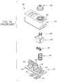
- Fig. 19 is an exploded perspective view illustrating a switch device 900 of Japanese Unexamined Patent Application Publication No. 2015-72894 (conventional example).
- Fig. 20 is a vertical sectional view illustrating the switch device 900 of the conventional example.
- the switch device 900 shown in Fig. 19 and Fig. 20 includes a box-shaped case 903 that has a through portion 3K1 and has an open bottom, a holding member 902 that covers the bottom of the case 903, a cover member 905 disposed so as to cover the through portion 3K1, a moving member 906 having an operation portion 963 protruding through the through portion 3K1, a biasing member 908 that returns the moving member 906 to an initial state before operation, a movable contact 907 that moves with the movement of the moving member 906, a common fixed contact 925 that is always in contact with the movable contact 907, a first switching fixed contact 926 and a second switching fixed contact 927 whose contact state with the movable contact 907 is switched by the movement of the movable contact 907, a first output terminal 922 and a second output terminal 923 that protrude downward from the holding member 902 and output signals to the outside, and two resistors 909 for obtaining the resistance value (voltage value) between these output
- metal members such as the fixed contacts (first switching fixed contact 926 and second switching fixed contact 927) and the output terminals (first output terminal 922 and second output terminal 923) are partially embedded in synthetic resin material of the holding member 902 by insert-molding.
- Two resistors 909 are soldered to parts of metal members that are exposed from synthetic resin material of the holding member 902.
- the present invention solves the above-described problem, and provides a switch device whose cost can be reduced and that has built-in resistors, and a method for manufacturing the same.
- a switch device in an aspect of the present invention, includes a housing having a through portion, a moving member provided with an operation portion exposed from the through portion, a biasing member that returns the moving member to an initial state before operation, a movable contact that moves with the movement of the moving member, a common fixed contact that is always in contact with the movable contact, a first switching fixed contact, the first switching fixed contact being in contact with the movable contact in the initial state where the operation portion is not operated, the first switching fixed contact coming out of contact with the movable contact with the operation of the operation portion, a second switching fixed contact, the second switching fixed contact being out of contact with the movable contact in the initial state where the operation portion is not operated, the second switching fixed contact coming into contact with the movable contact with the operation of the operation portion, extending portions that extend from at least two of the common fixed contact, the first switching fixed contact, and the second switching fixed contact, at least two terminal members that extend from the housing to the outside, and two resistors for obtaining the resistance value between the
- the housing includes a box-shaped case that has the through portion and has an open bottom, and a holding member in which the terminal members are embedded and that covers the bottom of the case. Some of the extending portions and the terminal members have fixing portions to which the resistors are soldered.
- the holding member includes a bottom wall portion that covers the bottom of the case, and a holding wall portion provided above the bottom wall portion and holding the fixing portions.
- the holding wall portion is formed of a first synthetic resin material having heat resistance
- the bottom wall portion is made of a second synthetic resin material having a heat distortion temperature lower than that of the first synthetic resin material.
- the holding wall portion can withstand the temperature of soldering such as reflow soldering, and the resistors can be reliably soldered to the fixing portions.
- the switch device since the switch device has the bottom wall portion separately from the holding wall portion, the bottom wall portion can be made of inexpensive material that need not withstand the temperature during soldering. The cost of the switch device can thereby be suppressed.
- terminal members extend from the bottom wall portion to the outside, and a part of each terminal member be surrounded, throughout its circumference, by the second synthetic resin material forming the bottom wall portion.
- Each terminal member can adhere, throughout its circumference, to the bottom wall portion. Therefore, water and the like can be prevented from entering through the gap between each terminal member and the bottom wall portion.
- the holding wall portion be disposed in a sealed housing space formed by the case and the bottom wall portion.
- a part of the holding wall portion is not exposed outside the housing, and the joint (interface) between the holding wall portion and the bottom wall portion and the joint between the holding wall portion and the case are not exposed to the outside. Therefore, only the joint between the case and the bottom wall portion is exposed to the outside, and it is not necessary to consider the adhesion between the holding wall portion and the bottom wall portion and between the holding wall portion and the case. Therefore, the degree of freedom of selection of synthetic resin material of the holding wall portion can be improved.
- the holding wall portion have, in the lower part thereof, embedded portions embedded in the bottom wall portion, and the embedded portions be each provided with an engaging portion formed such that the lower part thereof is larger than the upper part thereof.
- the holding wall portion is formed of the first synthetic resin material, and the bottom wall portion is formed of the second synthetic resin material different from the first synthetic resin material, the firmness of engagement (adhesion) therebetween can be improved. Therefore, for example, in the assembly step, the holding wall portion and the bottom wall portion can be easily handled as an integrated component.
- the case be formed of a third synthetic resin material having a heat distortion temperature lower than that of the first synthetic resin material.
- the case can be made of inexpensive material that need not withstand the temperature during soldering. Therefore, the cost of the switch device can be further suppressed.
- the second synthetic resin material and the third synthetic resin material be the same type of material.
- the holding member and the case When integrating the holding member and the case, laser welding can be suitably used. Therefore, the holding member and the case can be easily integrated, and the adhesion and joint strength between the holding member and the case can be improved. Therefore, the airtightness between the holding member and the case can be improved, and the cost of the switch device can be further suppressed.
- a method for manufacturing a switch device including a housing having a through portion, a moving member provided with an operation portion exposed from the through portion, a biasing member that returns the moving member to an initial state before operation, a movable contact that moves with the movement of the moving member, a common fixed contact that is always in contact with the movable contact, a first switching fixed contact, the first switching fixed contact being in contact with the movable contact in the initial state where the operation portion is not operated, the first switching fixed contact coming out of contact with the movable contact with the operation of the operation portion, a second switching fixed contact, the second switching fixed contact being out of contact with the movable contact in the initial state where the operation portion is not operated, the second switching fixed contact coming into contact with the movable contact with the operation of the operation portion, extending portions that extend from at least two of the common fixed contact, the first switching fixed contact, and the second switching fixed contact, at least two terminal members that extend from the housing to the outside, and two resistors for
- the housing includes a box-shaped case that has the through portion and has an open bottom, and a holding member in which the terminal members are embedded and that covers the bottom of the case. Some of the extending portions and the terminal members have fixing portions to which the resistors can be soldered.
- the holding member includes a bottom wall portion that covers the bottom of the case, and a holding wall portion provided above the bottom wall portion and holding the fixing portions.
- the holding wall portion is formed of a first synthetic resin material having heat resistance
- the bottom wall portion is made of a second synthetic resin material having a heat distortion temperature lower than that of the first synthetic resin material.
- the method includes a first molding step in which the holding wall portion is formed, with the fixing portions exposed, by insert-molding a metal member having the fixing portions using the first synthetic resin material, a resistor mounting step in which the resistors are soldered to the fixing portions, and a second molding step in which the bottom wall portion is formed by insert-molding the terminal members located on the lower side of the holding wall portion using the second synthetic resin material.
- the resistors can be reliably soldered to the fixing portions by high-temperature heating.
- the bottom wall portion can be made of inexpensive material that need not withstand the temperature during soldering, and the manufacturing cost of the switch device can be suppressed.
- the resistor mounting step include a reflow step in which solder paste provided between the fixing portions and electrode portions of the resistors is heated.
- the resistors can be soldered to the fixing portions with high productivity.
- the bottom wall portion be formed such that a part of each terminal member is surrounded, throughout its circumference, by the second synthetic resin material, and such that the terminal members extend from the bottom wall portion to the outside.
- Each terminal member can adhere, throughout its circumference, to the bottom wall portion. Therefore, water and the like can be prevented from entering through the gap between each terminal member and the bottom wall portion.
- the bottom wall portion be formed such that the lower part of the holding wall portion is embedded in the bottom wall portion, and such that the holding wall portion is not exposed on the lower side of the bottom wall portion.
- a part of the holding wall portion is not exposed outside the housing. Therefore, the joint between the holding wall portion and the bottom wall portion and the joint between the holding wall portion and the case are not exposed to the outside, and only the joint between the case and the bottom wall portion is exposed to the outside. Therefore, it is not necessary to consider the adhesion between the holding wall portion and the bottom wall portion and between the holding wall portion and the case, and the degree of freedom of selection of synthetic resin material of the holding wall portion can be improved.
- an engaging portion having a shape such that the lower part thereof is larger than the upper part thereof be formed in each of embedded portions of the holding wall portion that are embedded in the bottom wall portion.
- the holding wall portion and the bottom wall portion can be easily handled as an integrated component. For example, even if the holding wall portion and the bottom wall portion are subjected to shock due to dropping or the like, they are not separated. The productivity of the switch device can thereby be improved.
- the method further include, before the first molding step, a frame body preparation step in which a frame body is prepared to which at least a part of each of the common fixed contact, the first switching fixed contact, the second switching fixed contact, the extending portions, and the terminal members is connected by a connecting portion, and, after the second molding step, a cutting step in which the connecting portions are cut.
- the insert molding in the first molding step, the soldering in the resistor mounting step, and the insert molding in the second molding step can be easily performed. Then, by cutting the connecting portions in the subsequent cutting step, the integrated component in which contacts and terminals are held by the holding member can be separated easily and as desired.
- the switch device can thereby be manufactured (made) with high productivity.
- the case be formed of a third synthetic resin material having a heat distortion temperature lower than that of the first synthetic resin material, and the second synthetic resin material and the third synthetic resin material be the same type of material.
- the case is formed of the third synthetic resin material having a heat distortion temperature lower than that of the first synthetic resin material, it is not necessary to use expensive synthetic resin material having heat resistance. Therefore, the manufacturing cost of the switch device can be further suppressed.
- the second synthetic resin material and the third synthetic resin material are the same type of material, when integrating the holding member and the case, laser welding can be suitably used. Therefore, the holding member and the case can be easily integrated, and the adhesion and joint strength between the holding member and the case can be improved. The airtightness of the housing is thereby improved, and the manufacturing cost of the switch device can be further suppressed.
- Fig. 1 is an exploded perspective view of a switch device 100.
- Fig. 2A is an upper perspective view of the switch device 100
- Fig. 2B is a lower perspective view of the switch device 100.
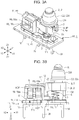
- Fig. 3A is a perspective view with the case K1 shown in Fig. 2A omitted
- Fig. 3B is a front view as seen from the Y2 side of Fig. 3A .
- Figs. 2A , 2B , 3A, and 3B show an initial state where an operation portion 2t is not operated.
- the switch device 100 of a first embodiment of the present invention has a box-like appearance shown in Figs. 2A and 2B , and as shown in Fig. 1 and Figs. 3A and 3B , it includes a housing 1 that forms an outer shape, a moving member 2 that is moved by operating an operation portion 2t, a biasing member 3 that returns the moving member 2 to the initial state before operation, a movable contact 4 that moves with the movement of the moving member 2, a common fixed contact G5 that is always in contact with the movable contact 4, a first switching fixed contact 15 and a second switching fixed contact 25 that come into and out of contact with the movable contact 4 with the operation of the operation portion 2t, extending portions 6 that extend from the common fixed contact G5, the first switching fixed contact 15, and the second switching fixed contact 25, terminal members T8 that extend from the housing 1 to the outside, two resistors R9 for obtaining the resistance value (voltage value) between two terminal members T8.
- the switch device 100 further has a housing 1 that forms an
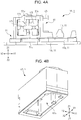
- Figs. 4A and 4B illustrate the housing 1, and Fig. 4A is a front view of a holding member H1 as seen from the Y2 side shown in Fig. 1 .
- Fig. 4B is a lower perspective view of the case K1 shown in Fig. 1 .
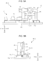
- Fig. 5A is a back view of the holding member H1 as seen from the Y1 side shown in Fig. 1
- Fig. 5B is a side view of the holding member H1 as seen from the X1 side shown in Fig. 1 .
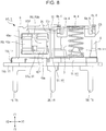
- Fig. 6 is an exploded perspective view of the holding member H1.
- Fig. 7 is a front view of the holding member H1 part shown in Fig.
- resistors R9 resistors R9a and R9b are shown in two-dot chain line, and solder fillets HDF are shown in dashed line.
- the housing 1 of the switch device 100 is formed of synthetic resin material, and includes a holding member H1 in which the terminal members T8 are embedded as shown in Fig. 4A , and a box-shaped case K1 having an open bottom as shown in Fig. 4B . As shown in Fig. 2B , the holding member H1 is disposed so as to cover the bottom of the case K1, and the holding member H1 and the case K1 are integrated.
- the holding member H1 of the housing 1 includes a bottom wall portion 11 that covers the bottom of the case K1 (see Fig. 2B ), and a holding wall portion 51 provided above the bottom wall portion 11.
- the holding wall portion 51 of the holding member H1 is formed of a first synthetic resin material having heat resistance that can withstand the temperature during soldering, is formed in a rectangular frame shape as shown in Fig. 4A and Fig. 5A , and is made by insert-molding the first switching fixed contact 15, the second switching fixed contact 25, and others shown in Fig. 7 .
- glass fiber-containing polyamide resin (PA) having a heat distortion temperature of about 250°C to 300°C is used as the first synthetic resin material.
- Glass fiber-containing polyphenylenesulfide resin (PPS) having a heat distortion temperature of about 250°C to 270°C, or glass fiber-containing liquid crystal polymer (LCP) having a heat distortion temperature of about 250°C to 360°C can also be suitably used as the first synthetic resin material.
- the heat distortion temperature as used herein is the temperature at which a synthetic resin material specimen deforms a specified amount under a specified load determined in accordance with a test standard, and is also referred to as deflection temperature under load. Since the melting temperature of general solder (lead-free solder) is 217°C to 220°C, as described later, the reflow temperature when reflow soldering electric components such as the resistors R9 to fixing portions 7A and 7B or the like is generally 220°C to 250°C. Therefore, the first synthetic resin material only has to have heat resistance that can withstand the reflow temperature, the temperature during soldering. Therefore, in the first embodiment of the present invention, the first synthetic resin material is not limited to those described above, and may be any other thermoplastic synthetic resin material having a heat distortion temperature higher than 250°C (the general upper limit of reflow temperature).
- the holding wall portion 51 has, in the lower part thereof, embedded portions 51m that are embedded in the bottom wall portion 11.
- the embedded portions 51m are each provided with an engaging portion 51k formed such that the lower part thereof is larger than the upper part thereof. Therefore, even when the bottom wall portion 11 is formed of a synthetic resin material different from the first synthetic resin material forming the holding wall portion 51, the firmness of engagement (adhesion) therebetween can be improved. Even when the holding wall portion 51 is formed of the first synthetic resin material, and the bottom wall portion 11 is formed of the second synthetic resin material different from the first synthetic resin material, the firmness of engagement (adhesion) therebetween can be improved. Therefore, for example, in the assembly step, the holding wall portion 51 and the bottom wall portion 11 can be easily handled as an integrated component.
- the holding wall portion 51 has an insulating portion 51r extending outward from the frame-like outer shape part. As shown in Fig. 7 , the insulating portion 51r is disposed so as to be sandwiched between the first switching fixed contact 15 and the second switching fixed contact 25. This ensures the insulation between the first switching fixed contact 15 and the second switching fixed contact 25. Although not shown in detail, the surface of the insulating portion 51r is flush with the surfaces of the first switching fixed contact 15 and the second switching fixed contact 25.
- the movable contact 4 (contact portions 4p described later) moves, the movable contact 4 can move smoothly because there is no difference in level between the first switching fixed contact 15 and the insulating portion 51r and between the insulating portion 51r and the second switching fixed contact 25.
- the frame-like inner part of the holding wall portion 51 has, as shown in Fig. 4A , a support portion 51s that supports, from behind, fixing portions 7A (described later) to which the resistors R9 shown in Fig. 7 are soldered, a first bar portion 51t disposed so as to separate two electrode portions R9e (described later, see Fig. 1 ) of each resistor R9, and a second bar portion 51u disposed so as to separate the two resistors R9 (resistors R9a and R9b).
- the bottom wall portion 11 of the holding member H1 is made by injection molding of a second synthetic resin material having a heat distortion temperature lower than that of the first synthetic resin material. Therefore, the bottom wall portion 11 can be made of inexpensive material that need not withstand the temperature during soldering.
- glass fiber-containing polybutylene terephthalate resin (PBT) having a heat distortion temperature of about 120°C to 220°C is used as the second synthetic resin material.
- Non-glass-fiber-containing polyacetal resin having a heat distortion temperature of about 90°C to 130°C, or glass fiber-containing polyacetal resin (POM) having a heat distortion temperature of about 110°C to 170°C can also be suitably used as the second synthetic resin material.
- Thermoplastic synthetic resin materials such as acrylonitrile butadiene styrene copolymer resin (ABS), polycarbonate resin (PC), and polyethylene terephthalate resin (PET) can also be used as the second synthetic resin material.
- the synthetic resin material used is selected in consideration of the usage environment or the like of the product to which the present invention is applied.
- the bottom wall portion 11 is formed in a rectangular plate shape and includes a base portion 11b that forms the bottom surface of the housing 1, a platform portion 11d that is inserted into the housing portion K1s of the case K1, a protruding portion 11f formed so as to protrude upward from the platform portion 11d, and a conical attachment portion 11t formed on the platform portion 11d.
- the terminal members T8 shown in Fig. 7 are partially embedded in the base portion 11b and the platform portion 11d of the bottom wall portion 11.
- the biasing member 3 is attached to the attachment portion 11t of the bottom wall portion 11 (see Figs. 3A and 3B ).
- the embedded portions 51m of the holding wall portion 51 are embedded in the platform portion 11d of the bottom wall portion 11, and the engaging portions 51k of the embedded portions 51m are engaged and integrated with the platform portion 11d of the bottom wall portion 11. Therefore, even when the holding wall portion 51 is formed of the first synthetic resin material and the bottom wall portion 11 is formed of the second synthetic resin material different from the first synthetic resin material, the firmness of engagement (adhesion) therebetween can be improved. Therefore, for example, in the assembly step, the holding wall portion 51 and the bottom wall portion 11 can be easily handled as an integrated component. For example, even if the holding wall portion 51 and the bottom wall portion 11 are subjected to shock due to dropping or the like during manufacturing, they are not separated.
- the holding member H1 is made by, after forming the holding wall portion 51, insert molding this holding wall portion 51, and forming the bottom wall portion 11.
- the protruding portion 11f of the bottom wall portion 11 is formed in an L shape so as to face and engage with the lower part of the holding wall portion 51. Therefore, even when the holding wall portion 51 is formed of the first synthetic resin material and the bottom wall portion 11 is formed of the second synthetic resin material different from the first synthetic resin material, the firmness of engagement (adhesion) therebetween can be improved.
- the case K1 of the housing 1 is formed of a third synthetic resin material having a heat distortion temperature lower than that of the first synthetic resin material, and is made by injection molding in a box-like shape having a housing portion K1s capable of housing the moving member 2, the biasing member 3, the movable contact 4, and others shown in Fig. 1 . Therefore, the case K1 can be made of inexpensive material that need not withstand the temperature during soldering.
- the second synthetic resin material and the third synthetic resin material are the same type of material. That is, in the first embodiment of the present invention, glass fiber-containing polybutylene terephthalate resin (PBT) having a heat distortion temperature of about 120°C to 220°C is used as the third synthetic resin material.
- Thermoplastic synthetic resin materials such as polyacetal resin (POM), acrylonitrile butadiene styrene copolymer resin (ABS), polycarbonate resin (PC), and polyethylene terephthalate resin (PET) can also be used as the third synthetic resin material.
- the second synthetic resin material is polybutylene terephthalate resin (PBT)
- the third synthetic resin material is the same type of polybutylene terephthalate resin (PBT). Therefore, when integrating the holding member H1 (bottom wall portion 11) and the case K1, laser welding can be suitably used. Therefore, the holding member H1 and the case K1 can be easily integrated, and the adhesion and joint strength between the holding member H1 and the case K1 can be improved. Therefore, the airtightness between the holding member H1 and the case K1 can be improved.
- guide portions that guide the moving member 2 so that the moving member 2 can be reciprocated in the vertical direction (Z direction shown in Figs. 2A and 2B ) are provided in the housing portion K1s of the case K1.
- a through portion K1h (see Fig. 1 ) through which an operation shaft portion 2j (described later) of the moving member 2 is passed is formed in the upper surface of the case K1. Although not shown, the operation shaft portion 2j protrudes from the through portion K1h to above the case K1.
- a cover member C2 that covers the protruding operation shaft portion 2j is disposed on the upper opening side of the through portion K1h.
- a groove portion K1m that engages with the lower part of the cover member C2 is provided in the opening of the through portion K1h shown in Fig. 1 .
- the cover member C2 is airtightly engaged with the groove portion K1m.
- the thus-configured housing 1 of the first embodiment of the present invention is formed by assembling and integrating the case K1 and the holding member H1.
- the above-described holding wall portion 51 is disposed in a sealed housing space formed by the case K1 and the bottom wall portion 11. Therefore, the holding wall portion 51 is not exposed outside the housing 1, and the joint (interface) between the holding wall portion 51 and the bottom wall portion 11 and the joint between the holding wall portion 51 and the case K1 are not exposed to the outside. Therefore, only the joint between the case K1 and the bottom wall portion 11 is exposed to the outside, and it is not necessary to consider the adhesion between the holding wall portion 51 and the bottom wall portion 11 and between the holding wall portion 51 and the case K1. Therefore, the degree of freedom of selection of synthetic resin material of the holding wall portion 51 can be improved. Even if the adhesion between the holding wall portion 51 and the bottom wall portion 11 is poor, water does not enter through this interface, and therefore good waterproof effect can be obtained.
- the moving member 2 of the switch device 100 mainly includes an operation base portion 2k that holds the movable contact 4 in the housing 1, an operation shaft portion 2j protruded from the upper surface of the operation base portion 2k, and an operation portion 2t formed at the distal end of the operation shaft portion 2j.
- the moving member 2 is configured to move vertically when the operation portion 2t is operated.
- the operation base portion 2k of the moving member 2 has a substantially U-shaped recessed portion 2r that houses the movable contact 4.
- a connection base portion 4r of the movable contact 4 described later is fixed to the ceiling surface of the recessed portion 2r by caulking or the like.
- the operation base portion 2k has, on the side surfaces thereof, outwardly protruding stepped portions 2d (see Fig. 1 ).
- the stepped portions 2d engage with the guide portions provided in the housing portion K1s of the case K1 so that the moving member 2 can reciprocate vertically.
- the operation shaft portion 2j of the moving member 2 is formed in a cylindrical shape. Although not shown, the operation shaft portion 2j is passed through the through portion K1h of the case K1 and protrudes above the case K1.
- the operation portion 2t of the moving member 2 is formed at the distal end of the operation shaft portion 2j, and is exposed from the top of the cover member C2 as shown in Fig. 2A .
- the joint part between the operation shaft portion 2j and the operation portion 2t is recessed, and the top of the cover member C2 is airtightly engaged with this part.
- the operation portion 2t which is the distal end part of the moving member 2 (operation shaft portion 2j), is depressed, for example, by an actuator (not shown).
- the moving member 2 is formed of a synthetic resin material such as acrylonitrile butadiene styrene copolymer resin (ABS), polycarbonate resin (PC), or polyacetal resin (POM, polyoxymethylene), and the operation base portion 2k, the operation shaft portion 2j, and the operation portion 2t are integrally formed by injection molding or the like.
- ABS acrylonitrile butadiene styrene copolymer resin
- PC polycarbonate resin
- POM polyacetal resin
- the cover member C2 of the switch device 100 is formed of a flexible elastic material such as silicone rubber. As shown in Fig. 1 , the cover member C2 has a flange portion C2v that is engaged with the groove portion K1m of the case K1, a dome portion C2d that is formed continuously with the flange portion C2v, and a through-hole C2h that is formed substantially in the center of the dome portion C2d.
- the cover member C2 is disposed on the upper surface of the case K1 so as to cover the through portion K1h, the flange portion C2v is engaged with the groove portion K1m, and the through-hole C2h is engaged with the recessed joint part between the operation shaft portion 2j and the operation portion 2t.
- the operation portion 2t which is the distal end part of the operation shaft portion 2j, is thereby exposed from the through-hole C2h of the cover member C2.
- the flange portion C2v may be firmly fixed to the case K1 by inwardly deforming the ring-like resin wall portion around the opening of the case K1 by caulking.
- the dome portion C2d of the cover member C2 is formed so as to have a small wall thickness, and is configured to be easily reversely deformed with the vertical motion (reciprocal motion) of the operation portion 2t (operation shaft portion 2j). Therefore, the dome portion C2d does not adversely affect the motion of the moving member 2. Thus, the entrance of dust, water, and the like into the switch device 100 can be prevented by the cover member C2.
- Fig. 8 is a front view showing a state where the biasing member 3, the movable contact 4, and the resistors R9 are disposed in the front view of Fig. 7 .
- the biasing member 3 of the switch device 100 is suitably a general coil spring as shown in Fig. 1 and Fig. 8 . As shown in Fig. 8 , one end of the biasing member 3 is attached to and supported by the attachment portion 11t of the holding member H1, and the other end thereof is in contact with the connection base portion 4r of the movable contact 4 (the ceiling surface of the moving member 2). The biasing member 3 elastically biases the moving member 2 and the movable contact 4 toward the upper surface of the case K1 (in the Z1 direction shown in Fig. 8 ).
- the biasing member 3 is disposed so as to be between the common fixed contact G5 and the first and second switching fixed contacts 15 and 25.
- the movable contact 4 can thereby be held in a balanced manner, and the movable contact 4 (contact portions 4p described later) can be stably brought into contact with the common fixed contact G5, the first switching fixed contact 15, and the second switching fixed contact 25.
- the coil spring serving as the biasing member 3 When the operation portion 2t is depressed, for example, by an actuator (not shown), the coil spring serving as the biasing member 3 is compressed by the movement of the moving member 2 and the movable contact 4. When the operation portion 2t is released from depression, the coil spring pushes back and returns the moving member 2 and the movable contact 4 to the initial state with the accumulated force thereof.
- the coil spring is a so-called returning member.
- a coil spring is suitably used as the biasing member 3, the present invention is not limited to this.
- the biasing member 3 only has to have function to return the moving member 2 to the initial state before operation.
- the biasing member 3 may be, for example, a leaf spring or a rubber member.
- the movable contact 4 of the switch device 100 is a conductive metal plate formed by bending an elastic metal plate, and includes a connection base portion 4r formed in a flat plate shape, a pair of opposite elastic arm portions 4a connected to the connection base portion 4r, and contact portions 4p provided at the free distal ends of the pair of elastic arm portions 4a.
- the conductive metal plate is made of copper, iron, or an alloy mainly composed of them, and the surface thereof is plated, for example, with nickel or silver.
- the pair of elastic arm portions 4a of the movable contact 4 are formed at one end and the other end of the connection base portion 4r.
- One of the pair of elastic arm portions 4a corresponds to the first switching fixed contact 15 and the second switching fixed contact 25, and the other corresponds to the common fixed contact G5.
- the pair of elastic arm portions 4a are formed in a substantially U shape in front view (as seen from the Y2 side of Fig. 1 ), and their free ends not connected to the connection base portion 4r extend in the protruding direction of the operation portion 2t (the Z1 direction shown in Fig. 8 ).
- the contact portions 4p of the movable contact 4 are in contact with the common fixed contact G5 and the first switching fixed contact 15 and out of contact with the second switching fixed contact 25.
- Fig. 9 is a front view with the holding member H1 shown in Fig. 7 omitted.
- resistors R9 resistor R9a and resistor R9b are shown in two-dot chain line.
- the first switching fixed contact 15, the second switching fixed contact 25, the common fixed contact G5, the extending portions 6, and the terminal members T8 of the switch device 100 are made of conductive material such as copper, iron, or an alloy mainly composed of them, by punching a sheet of metal member, so as to have independent shapes as shown in Fig. 9 . These are insert-molded before being separated, and are held by the holding member H1.
- the surface of the metal member is plated, for example, with nickel or silver.
- the first switching fixed contact 15, the second switching fixed contact 25, the common fixed contact G5, the extending portions 6, and the terminal members T8 are disposed on substantially the same plane.
- the first switching fixed contact 15 of the switch device 100 is in contact with the contact portion 4p of the movable contact 4.
- the first switching fixed contact 15 comes out of contact with the contact portion 4p of the movable contact 4 with the downward operation of the operation portion 2t.
- the second switching fixed contact 25 of the switch device 100 is out of contact with the contact portion 4p of the movable contact 4.
- the second switching fixed contact 25 comes into contact with the contact portion 4p of the movable contact 4 with the operation of the operation portion 2t, and the switch device 100 is brought to a switched state.
- the common fixed contact G5 of the switch device 100 is always in contact with the movable contact 4 in both the initial state shown in Fig. 8 and the switched state where the movable contact 4 is moved with the operation of the operation portion 2t.
- the extending portions 6 of the switch device 100 are formed so as to extend from the common fixed contact G5, the first switching fixed contact 15, and the second switching fixed contact 25.
- some of the extending portions 6 have fixing portions 7A to which the electrode portions R9e of the resistors R9 are soldered.
- the extending portions 6 having the fixing portions 7A are held by the holding wall portion 51 of the holding member H1 with the fixing portions 7A exposed.
- the terminal members T8 of the switch device 100 extend from the bottom wall portion 11 to the outside and includes a first terminal 18 electrically connected to the first switching fixed contact 15 through the resistor R9a, a second terminal 28 electrically connected to the second switching fixed contact 25 through the resistor R9b, and a common terminal 58 electrically connected to the common fixed contact G5.
- some of the terminal members T8 (the first terminal 18 and the second terminal 28) have fixing portions 7B to which the electrode portions R9e of the resistors R9 are soldered.
- the first terminal 18 and the second terminal 28 are held by the holding wall portion 51 of the holding member H1 with the fixing portions 7B exposed.
- the fixing portions 7A provided in the extending portions 6 and the fixing portions 7B provided in the terminal members T8 are exposed in the frame-like inner part of the holding wall portion 51 and are held by the holding wall portion 51, when placing the resistors R9a and R9b on their respective fixing portions 7A and 7B and performing soldering, soldering such as reflow soldering can be performed. That is, since the holding wall portion 51 holding the fixing portions 7A and 7B is formed of the first synthetic resin material having heat resistance, the holding wall portion 51 can withstand the temperature of soldering such as reflow soldering, and the resistors R9 can be reliably soldered to the fixing portions 7A and 7B.
- each terminal member T8 is surrounded, throughout its circumference, by the second synthetic resin material forming the bottom wall portion 11. Therefore, each terminal member T8 can adhere, throughout its circumference, to the bottom wall portion 11. Therefore, water and the like can be prevented from entering through the gap between each terminal member T8 and the bottom wall portion 11.
- the switch device 100 is formed by assembling and integrating the case K1 and the holding member H1, and the holding wall portion 51 is disposed in a sealed housing space formed by the case K1 and the bottom wall portion 11, the waterproof performance of the switch device 100 can be improved.
- resistors R9 of the switch device 100 Two inexpensive general-purpose chip resistors are used as the resistors R9 of the switch device 100, and chip resistors having different resistance values are selected as the resistor R9a and R9b.
- the two resistors R9 (resistors R9a and R9b) are each soldered to the fixing portions 7A and 7B corresponding to two electrode portions R9e.
- the first switching fixed contact 15 and the first terminal 18 that are separated from each other, and the second switching fixed contact 25 and the second terminal 28 that are separated from each other are thereby electrically connected by the resistors R9a and R9b.
- chip resistors are suitably used as the resistors R9, the present invention is not limited to this.
- the resistors R9 may each be, for example, a substrate on which a carbon resistor is printed.
- Fig. 10 is a detection circuit diagram of the switch device 100.
- Fig. 10 shows the initial state where the operation portion 2t is not operated.
- parts corresponding to components of the switch device 100 are indicated with dashed lines.
- the common fixed contact G5 connected to the common terminal 58 through the extending portion 6 is connected through the movable contact 4 to the first switching fixed contact 15 in the initial state where the operation portion 2t is not operated.
- the first switching fixed contact 15 is connected through the resistor R9a to the first terminal 18.
- one end of the resistor R9a is connected to the fixing portion 7A of the extending portion 6, and the other end of the resistor R9a is connected to the fixing portion 7B of the first terminal 18 (terminal member T8).
- the second switching fixed contact 25 is not connected to the common fixed contact G5, and is connected through the resistor R9b to the second terminal 28.
- one end of the resistor R9b is connected to the fixing portion 7A of the extending portion 6, and the other end of the resistor R9b is connected to the fixing portion 7B of the second terminal 28 (terminal member T8).
- the switch device 100 is brought to the switched state.
- the operation portion 2t is released from depression, as described above, the movable contact 4 is pushed back to the initial state by the biasing member 3 (returning member). In this way, the switch device 100 is switched between the initial state and the switched state.
- the resistance value of the resistor R9a is detected between the first terminal 18 and the common terminal 58, and open (infinite) resistance value is detected between the second terminal 28 and the common terminal 58.
- open (infinite) resistance value is detected between the first terminal 18 and the common terminal 58, and the resistance value of the resistor R9b is detected between the second terminal 28 and the common terminal 58. The on/off of the switch can thereby be detected.
- the detection circuit when a wire or the like of an external device connected is in an open circuit state, for example, the voltage from the external device is not applied to the common terminal 58, regardless of the connection state of the movable contact 4 (the resistance value as the detection circuit is seen from the external device is detected to be infinite).
- the wire or the like of the external device when the wire or the like of the external device is in a short circuit state, the voltage of power source supplied to the external device is applied to the common terminal 58, regardless of the connection state of the movable contact 4 (the resistance value as the detection circuit is seen from the external device is detected to be zero).
- this detection circuit when the external device connected is in a normal state, for example, different voltage values are detected at the common terminal 58 depending on the connection state of the movable contact 4. That is, in the initial state, a voltage corresponding to the resistance value of the resistor R9a and the resistance value of the external device is applied to the common terminal 58, and in the switched state, a voltage corresponding to the resistance value of the resistor R9b and the resistance value of the external device is applied to the common terminal 58.
- the voltage (resistance value) of this detection circuit it can be detected whether the connection between the external device and the wire is normal or abnormal.
- the holding wall portion 51 holding the fixing portions 7A and 7B is formed of the first synthetic resin material having heat resistance, during soldering such as reflow soldering, the holding wall portion 51 can withstand the temperature of soldering such as reflow soldering, and the resistors R9 can be reliably soldered to the fixing portions 7A and 7B.
- the switch device 100 since the switch device 100 has the bottom wall portion 11 of the holding member H1 separately from the holding wall portion 51 of the holding member H1, the bottom wall portion 11 can be made of inexpensive material that need not withstand the temperature during soldering. The cost of the switch device 100 can thereby be suppressed.
- each terminal member T8 Since a part of each terminal member T8 is surrounded, throughout its circumference, by the second synthetic resin material forming the bottom wall portion 11, each terminal member T8 can adhere, throughout its circumference, to the bottom wall portion 11. Therefore, water and the like can be prevented from entering through the gap between each terminal member T8 and the bottom wall portion 11.
- the holding wall portion 51 is disposed in a housing space formed by the case K1 and the bottom wall portion 11, a part of the holding wall portion 51 is not exposed outside the housing 1, and the joint (interface) between the holding wall portion 51 and the bottom wall portion 11 and the joint between the holding wall portion 51 and the case K1 are not exposed to the outside. Therefore, only the joint between the case K1 and the bottom wall portion 11 is exposed to the outside, and it is not necessary to consider the adhesion between the holding wall portion 51 and the bottom wall portion 11 and between the holding wall portion 51 and the case K1. Therefore, the degree of freedom of selection of synthetic resin material of the holding wall portion 51 can be improved.
- the embedded portions 51m provided in the lower part of the holding wall portion 51 are each provided with an engaging portion 51k formed such that the lower part thereof is larger than the upper part thereof, and the engaging portions 51k are embedded in the bottom wall portion 11, even when the holding wall portion 51 is formed of the first synthetic resin material, and the bottom wall portion 11 is formed of the second synthetic resin material different from the first synthetic resin material, the firmness of engagement (adhesion) therebetween can be improved. Therefore, for example, in the assembly step, the holding wall portion 51 and the bottom wall portion 11 can be easily handled as an integrated component.
- the case K1 is formed of the third synthetic resin material having a heat distortion temperature lower than that of the first synthetic resin material, the case K1 can be made of inexpensive material that need not withstand the temperature during soldering. Therefore, the cost of the switch device 100 can be further suppressed.
- the second synthetic resin material and the third synthetic resin material are the same type of material, when integrating the holding member H1 (bottom wall portion 11) and the case K1, laser welding can be suitably used. Therefore, the holding member H1 and the case K1 can be easily integrated, and the adhesion and joint strength between the holding member H1 and the case K1 can be improved. Therefore, the airtightness between the holding member H1 and the case K1 can be improved, and the cost of the switch device 100 can be further suppressed.
- Fig. 11 illustrates a method for manufacturing the switch device 100 according to the first embodiment of the present invention, and illustrates each manufacturing step.
- Figs. 12A and 12B are front views illustrating a frame body preparation step P1, Fig. 12A shows a metal member before processing, and Fig. 12B shows a state where the frame body preparation step P1 is finished.
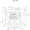
- Fig. 13 is a front view illustrating a first molding step P2, and shows a state where the first molding step P2 is finished.
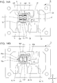
- Figs. 14A and 14B are front views illustrating a resistor mounting step P3, Fig. 14A shows a state where solder paste HDP is applied to fixing portions 7A and 7B, and Fig. 14B shows a state where a reflow step PR3 is finished.
- Fig. 14A solder paste HDP is cross-hatched.
- Fig. 15A is a front view illustrating a second molding step P4, and shows a state where the second molding step P4 is finished.
- Fig. 15B is a front view illustrating a cutting step P5, and shows a state where the cutting step P5 is finished.
- Fig. 12A to Fig. 15B for ease of understanding, one frame body 10 is shown, a so-called hoop-like frame body such that a plurality of frame bodies are joined together to form a continuous band may be used.
- the method for manufacturing the switch device 100 in the first embodiment of the present invention mainly includes a frame body preparation step P1 in which a frame body 10 is prepared to which terminal members T8 and others are connected by connecting portions 10r, a first molding step P2 in which a holding wall portion 51 is formed, a resistor mounting step P3 in which resistors R9 are soldered, a second molding step P4 in which a bottom wall portion 11 is formed, and a cutting step P5 in which the connecting portions 10r are cut.
- the method for manufacturing the switch device 100 further includes an assembly step K6 in which members passed through each step are assembled, and a joining step S7 in which after the assembly step K6, a holding member H1 and a case K1 are joined together.
- a conductive metal plate made of conductive material such as copper, iron, or an alloy mainly composed of them is prepared. Then, punching is performed on this conductive metal plate using a die.
- a frame body 10 is prepared to which a part of each of a common fixed contact G5, a first switching fixed contact 15, a second switching fixed contact 25, extending portions 6, and terminal members T8 is connected by a connecting portion 10r.
- the frame body 10 that is a metal member is provided with fixing portions 7A and 7B required in the subsequent resistor mounting step P3. Needless to say, the frame body preparation step P1 must be performed before the subsequent first molding step P2.
- the frame body 10 that is a metal member is insert-molded using a first synthetic resin material having heat resistance, and as shown in Fig. 13 , a rectangular frame-like holding wall portion 51 is formed so as to sandwich the metal member.
- the holding wall portion 51 is formed such that the surfaces of the fixing portions 7A and 7B are exposed in the frame-like inner part of the holding wall portion 51.
- the holding wall portion 51 when forming the holding wall portion 51, as shown in Fig. 13 , the holding wall portion 51 is formed such that the surfaces of the first switching fixed contact 15 and the second switching fixed contact 25 are exposed in the frame-like outer part of the holding wall portion 51. At that time, an insulating portion 51r of the holding wall portion 51 is disposed between the first switching fixed contact 15 and the second switching fixed contact 25, and the first switching fixed contact 15 and the second switching fixed contact 25 are fixed.
- the extending portions 6 and the terminal members T8 are partially embedded in the holding wall portion 51 and fixed.
- embedded portions 51m that are embedded in the bottom wall portion 11 formed in the second molding step P4 are formed in the holding wall portion 51, and an engaging portion 51k having a shape such that the lower part thereof is larger than the upper part thereof is formed in each of the embedded portions 51m.
- the holding wall portion 51 having many functions can be easily made.
- thermoplastic synthetic resin material such as polyamide resin (PA) or polyphenylenesulfide resin (PPS) is used as the first synthetic resin material
- the holding wall portion 51 can be formed by injection molding, more easily and inexpensively.
- the resistor mounting step P3 includes a mounting step PM3 in which resistors R9 are mounted on the fixing portions 7A and 7B, and a reflow step PR3 in which the resistors R9 are soldered to the fixing portions 7A and 7B.
- solder paste HDP is applied to parts of the fixing portions 7A and 7B held by the holding wall portion 51.
- two resistors R9a and R9b are mounted on the parts to which solder paste HDP is applied.
- solder paste HDP is interposed between the electrode portions R9e of the resistors R9 (resistors R9a and R9b) and the fixing portions 7A and 7B.
- a dispenser device is suitably used for applying solder paste HDP
- a surface mounting device is suitably used for mounting the resistors R9.
- the frame body 10 on which the resistors R9 are mounted is loaded into a reflow furnace, and solder paste HDP provided between the electrode portions R9e of the resistors R9 and the fixing portions 7A and 7B is heated.
- the resistors R9 are thereby soldered and fixed to the fixing portions 7A and 7B as shown in Fig. 14B .
- the holding wall portion 51 formed in the first molding step P2 is formed of the first synthetic resin material having heat resistance that can withstand the temperature during soldering, the resistors R9 can be reliably soldered to the fixing portions 7A and 7B by high-temperature heating. Moreover, since soldering is performed using a reflow furnace in the reflow step PR3, the resistors R9 can be soldered to the fixing portions 7A and 7B with high productivity. "Having heat resistance” means having heat resistance such that when soldering the resistors R9, the holding wall portion 51 (first synthetic resin material) is neither thermally deformed nor melted.
- “having heat resistance” means having heat resistance such that when exposed to the reflow temperature (generally 220°C to 250°C) for a short time (30 to 40 seconds), the holding wall portion 51 is neither thermally deformed nor melted.
- the frame body 10 passed through the resistor mounting step P3 is insert-molded, and as shown in Fig. 15A , a bottom wall portion 11 is formed such that the terminal members T8 located on the lower side of the holding wall portion 51 are embedded therein.
- the bottom wall portion 11 is formed such that the embedded portions 51m formed in the lower part of the holding wall portion 51 are embedded therein. Since the bottom wall portion 11 is not exposed to high temperature by soldering in the subsequent steps, a second synthetic resin material having a heat distortion temperature lower than that of the first synthetic resin material can be used as synthetic resin material of the bottom wall portion 11. Therefore, the bottom wall portion 11 can be made of inexpensive synthetic resin material that need not withstand the temperature during soldering, and this manufacturing method can suppress the cost of the switch device 100.
- the engaging portions 51k formed in the embedded portions 51m of the holding wall portion 51 are embedded in the bottom wall portion 11. Therefore, after the second molding step P4, even when the bottom wall portion 11 is formed of the second synthetic resin material, and the holding wall portion 51 is formed of the first synthetic resin material different from the second synthetic resin material, the firmness of engagement (adhesion) therebetween can be improved. Therefore, for example, in the assembly step, the holding wall portion 51 and the bottom wall portion 11 can be easily handled as an integrated component. For example, even if the holding wall portion 51 and the bottom wall portion 11 are subjected to shock due to dropping or the like, they are not separated. The productivity of the switch device 100 can thereby be improved.
- the bottom wall portion 11 is formed such that a part of each terminal member T8 is surrounded, throughout its circumference, by the second synthetic resin material of the bottom wall portion 11. Therefore, each terminal member T8 can adhere, throughout its circumference, to the bottom wall portion 11. Therefore, water and the like can be prevented from entering through the gap between each terminal member T8 and the bottom wall portion 11.
- the bottom wall portion 11 is formed such that the holding wall portion 51 is not exposed on the lower side of the bottom wall portion 11. Therefore, a part of the holding wall portion 51 is not exposed outside the housing 1. Therefore, the joint between the holding wall portion 51 and the bottom wall portion 11 and the joint between the holding wall portion 51 and the case K1 are not exposed to the outside, and only the joint between the case K1 and the bottom wall portion 11 is exposed to the outside. Therefore, it is not necessary to consider the adhesion between the holding wall portion 51 and the bottom wall portion 11 and between the holding wall portion 51 and the case K1, and the degree of freedom of selection of synthetic resin material of the holding wall portion 51 can be improved.
- the insert molding in the first molding step P2 the soldering in the resistor mounting step P3, and the insert molding in the second molding step P4 can be easily performed.
- the assembly step K6 in which components are assembled is performed.
- assembly is performed using the integrated component made in steps P1 to P5, the movable contact 4 made in the movable contact preparation step J1, the moving member 2 made in the moving member preparation step J2, the biasing member 3 made in the biasing member preparation step J3, the case K1 made in the case molding step J4, and the cover member C2 made in the cover member preparation step J5.
- one end of a coil spring that is the biasing member 3 is attached and fixed to the attachment portion 11t of the bottom wall portion 11 in the integrated component (see Fig. 15B ).
- the movable contact 4 is housed in the substantially U-shaped recessed portions 2r of the moving member 2, and the connection base portion 4r of the movable contact 4 is fixed to the ceiling surface of the recessed portion 2r by caulking or the like. Then, the movable contact 4 is disposed such that the connection base portion 4r of the movable contact 4 is in contact with the other end of the coil spring (biasing member 3), and the movable contact 4 is assembled such that a pair of elastic arm portions 4a (contact portions 4p) provided at one end of the connection base portion 4r of the movable contact 4 sandwich the first switching fixed contact 15, and a pair of elastic arm portions 4a (contact portions 4p) provided at the other end of the connection base portion 4r sandwich the common fixed contact G5.
- the case K1 is disposed so as to cover and house the upper surface side of the holding member H1.
- the operation shaft portion 2j of the moving member 2 is passed through the through portion K1h of the case K1 such that the operation shaft portion 2j protrudes above the case K1.
- the case K1 since the case K1 is not exposed to high temperature by soldering in the subsequent steps, a third synthetic resin material having a heat distortion temperature lower than that of the first synthetic resin material can be used as synthetic resin material of the case K1. Therefore, the case K1 can be made of inexpensive synthetic resin material that need not withstand the temperature during soldering, and the cost of the switch device 100 can be suppressed.
- the assembly step K6 is finished.
- the cover member C2 is disposed on the upper surface of the case K1 so as to cover the through portion K1h of the case K1.
- the flange portion C2v of the cover member C2 is engaged with the groove portion K1m of the case K1
- the through-hole C2h of the cover member C2 is engaged with the recessed joint part between the operation shaft portion 2j and the operation portion 2t.
- the flange portion C2v may be firmly fixed to the case K1 by inwardly deforming the ring-like resin wall portion around the opening of the case K1 by caulking.
- the flange portion C2v may be firmly fixed to the case K1 by applying adhesive to the flange portion C2v and the resin wall portion and hardening the adhesive.
- the joining step S7 is performed, and the switch device 100 shown in Figs. 2A and 2B is completed.
- the bottom wall portion 11 of the holding member H1 and the case K1 are integrated.
- Laser welding is suitably used for this integration.
- the holding member H1 (bottom wall portion 11) and the case K1 can be easily integrated, and the adhesion and joint strength between the holding member H1 and the case K1 can be improved.
- the second synthetic resin material forming the bottom wall portion 11 of the holding member H1 and the third synthetic resin material forming the case K1 are the same type of material, the adhesion and joint strength can be further improved.
- the airtightness of the housing 1 can be improved.
- the holding wall portion 51 formed in the first molding step P2 is formed of the first synthetic resin material having heat resistance. Therefore, in the resistor mounting step P3, the resistors R9 can be reliably soldered to the fixing portions 7A and 7B by high-temperature heating.
- the bottom wall portion 11 can be formed using the second synthetic resin material having a heat distortion temperature lower than that of the first synthetic resin material. Therefore, the bottom wall portion 11 can be made of inexpensive material that need not withstand the temperature during soldering, and this manufacturing method can suppress the manufacturing cost of the switch device 100.
- the resistor mounting step P3 includes the reflow step PR3
- the resistors R9 can be soldered to the fixing portions 7A and 7B with high productivity.
- each terminal member T8 can adhere, throughout its circumference, to the bottom wall portion 11. Therefore, water and the like can be prevented from entering through the gap between each terminal member T8 and the bottom wall portion 11.
- the bottom wall portion 11 is formed such that the holding wall portion 51 is not exposed on the lower side of the bottom wall portion 11. Therefore, a part of the holding wall portion 51 is not exposed outside the housing 1. Therefore, the joint between the holding wall portion 51 and the bottom wall portion 11 and the joint between the holding wall portion 51 and the case K1 are not exposed to the outside, and only the joint between the case K1 and the bottom wall portion 11 is exposed to the outside. Therefore, it is not necessary to consider the adhesion between the holding wall portion 51 and the bottom wall portion 11 and between the holding wall portion 51 and the case K1, and the degree of freedom of selection of synthetic resin material of the holding wall portion 51 can be improved.
- the bottom wall portion 11 is formed such that the engaging portions 51k of the holding wall portion 51 formed in the first molding step P2 are embedded in the bottom wall portion 11. Therefore, after the second molding step P4, even when the bottom wall portion 11 is formed of the second synthetic resin material, and the holding wall portion 51 is formed of the first synthetic resin material different from the second synthetic resin material, the firmness of engagement (adhesion) therebetween can be improved. Therefore, for example, in the assembly step, the holding wall portion 51 and the bottom wall portion 11 can be easily handled as an integrated component. For example, even if the holding wall portion 51 and the bottom wall portion 11 are subjected to shock due to dropping or the like, they are not separated. The productivity of the switch device 100 can thereby be improved.
- the insert molding in the first molding step P2, the soldering in the resistor mounting step P3, and the insert molding in the second molding step P4 can be easily performed. Then, by cutting the connecting portions 10r in the subsequent cutting step P5, the integrated component in which contacts and terminals are held by the holding member H1 can be separated easily and as desired.
- the switch device 100 can thereby be manufactured (made) with high productivity.
- the case K1 is formed of the third synthetic resin material having a heat distortion temperature lower than that of the first synthetic resin material, it is not necessary to use expensive synthetic resin material having heat resistance. Therefore, the manufacturing cost of the switch device can be further suppressed.
- the second synthetic resin material and the third synthetic resin material are the same type of material, when integrating the holding member H1 (bottom wall portion 11) and the case K1, laser welding can be suitably used. Therefore, the holding member H1 and the case K1 can be easily integrated, and the adhesion and joint strength between the holding member H1 and the case K1 can be improved. The airtightness of the housing 1 is thereby improved, and the manufacturing cost of the switch device 100 can be further suppressed.
- the switch device 200 according to the second embodiment of the present invention differs from the first embodiment mainly in the configuration of the first switching fixed contact 35, the second switching fixed contact 45, and the terminal members T8.
- the same reference numerals will be used to designate the same components as those in the first embodiment, and the detailed description thereof will be omitted. Because the method for manufacturing the switch device 200 is the same as the method for manufacturing the switch device 100 of the first embodiment, the description thereof will be omitted.
- Fig. 16 is a perspective view of the switch device 200 according to the second embodiment of the present invention.
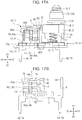
- Fig. 17A is a front view with the case K1 shown in Fig. 16 omitted
- Fig. 17B is a front view with the holding member H1, moving member 2, cover member C2, biasing member 3, movable contact 4 (see Fig. 8 ) and resistors R9 shown in Fig. 17A omitted.
- resistors R9 resistors R9 (resistors R9c and R9d) are shown in two-dot chain line.
- Fig. 16 and Fig. 17A show an initial state where the operation portion 2t is not operated.
- the switch device 200 of the second embodiment of the present invention has a box-like appearance shown in Fig. 16 , and includes a housing 1 that forms an outer shape, a moving member 2 that is moved by operating an operation portion 2t, a biasing member 3 that returns the moving member 2 to the initial state before operation, a movable contact 4 that moves with the movement of the moving member 2, a common fixed contact G5 that is always in contact with the movable contact 4, a first switching fixed contact 35 and a second switching fixed contact 45 that come into and out of contact with the movable contact 4 with the operation of the operation portion 2t, extending portions 6 that extend from the common fixed contact G5, the first switching fixed contact 15, and the second switching fixed contact 25, terminal members T8 that extend from the housing 1 to the outside, two resistors R9 for obtaining the resistance value (voltage value) between two terminal members T8.
- the switch device 200 further has a cover member C2 disposed on the upper side (Z1 side
- the first switching fixed contact 35, the second switching fixed contact 45, the common fixed contact G5, the extending portions 6, and the terminal members T8 of the switch device 200 according to the second embodiment of the present invention are made of conductive material such as copper, iron, or an alloy mainly composed of them, by punching a sheet of metal member, so as to have independent shapes as shown in Fig. 17B . These are insert-molded before being separated, and arc held by the holding member H1.
- the surface of the metal member is plated, for example, with nickel or silver.
- the first switching fixed contact 35 of the switch device 200 is in contact with the contact portion 4p of the movable contact 4.
- the first switching fixed contact 35 comes out of contact with the contact portion 4p of the movable contact 4 with the downward operation of the operation portion 2t.
- the second switching fixed contact 45 of the switch device 200 is out of contact with the contact portion 4p of the movable contact 4.
- the second switching fixed contact 45 comes into contact with the contact portion 4p of the movable contact 4 with the operation of the operation portion 2t, and the switch device 100 is brought to a switched state.
- the common fixed contact G5 of the switch device 200 is always in contact with the movable contact 4 in both the initial state and the switched state where the movable contact 4 is moved with the operation of the operation portion 2t.
- the extending portions 6 of the switch device 200 are formed so as to extend from the common fixed contact G5, the first switching fixed contact 35, and the second switching fixed contact 45.
- some of the extending portions 6 have fixing portions 7A to which the electrode portions R9e of the resistors R9 are soldered.
- the extending portions 6 having the fixing portions 7A are held by the holding wall portion 51 of the holding member H1 with the fixing portions 7A exposed.
- the terminal members T8 of the switch device 200 extend from the bottom wall portion 11 of the holding member H1 to the outside and includes a second terminal 48 electrically connected to the second switching fixed contact 45 through the resistor R9c, and a common terminal 68 electrically connected to the common fixed contact G5.
- the common fixed contact G5 (common terminal 68) and the second switching fixed contact 45 are electrically connected to each other through the resistor R9d.
- some of the terminal members T8 (the second terminal 48 and the common terminal 68) have fixing portions 7B to which the electrode portions R9e of the resistors R9 are soldered.
- the second terminal 48 and the common terminal 68 are held by the holding wall portion 51 of the holding member H1 with the fixing portions 7B exposed.
- the fixing portions 7A provided in the extending portions 6 and the fixing portions 7B provided in the terminal members T8 are exposed in the frame-like inner part of the holding wall portion 51 and are held by the holding wall portion 51, when placing the resistors R9c and R9d on their respective fixing portions 7A and 7B and performing soldering, soldering such as reflow soldering can be performed. That is, since the holding wall portion 51 holding the fixing portions 7A and 7B is formed of the first synthetic resin material having heat resistance, the holding wall portion 51 can withstand the temperature of soldering such as reflow soldering, and the resistors R9 can be reliably soldered to the fixing portions 7A and 7B.
- Fig. 18 is a detection circuit diagram of the switch device 200.
- Fig. 18 shows the initial state where the operation portion 2t is not operated.
- parts corresponding to components of the switch device 200 are indicated with dashed lines.
- the common fixed contact G5 connected to the common terminal 68 through the extending portion 6 is connected through the movable contact 4 to the first switching fixed contact 35 in the initial state where the operation portion 2t is not operated.
- the first switching fixed contact 35 is not in contact with any part, and is a dummy contact.
- the second switching fixed contact 45 is connected through the resistor R9d to the common terminal 68. At that time, one end of the resistor R9d is connected to the fixing portion 7A of the extending portion 6, and the other end of the resistor R9d is connected to the fixing portion 7B of the common terminal 68.
- the second switching fixed contact 45 is also connected through the resistor R9c to the second terminal 48. At that time, one end of the resistor R9c is connected to the fixing portion 7A of the extending portion 6, and the other end of the resistor R9c is connected to the fixing portion 7B of the second terminal 48 (terminal member T8).
- the switch device 200 is brought to the switched state.
- the operation portion 2t is released from depression, as described above, the movable contact 4 is pushed back to the initial state by the biasing member 3 (returning member). In this way, the switch device 100 is switched between the initial state and the switched state.
- the present invention is not limited to this.
- the bottom wall portion 11 and the case K1 may be integrated using an adhesive.
- joining can be performed with high adhesion and joint strength by using an adhesive.
- the holding wall portion 51 has the embedded portions 51m embedded in the bottom wall portion 11.
- the present invention is not limited to this.
- the holding wall portion 51 may be formed above the bottom wall portion 11.
Landscapes
- Engineering & Computer Science (AREA)
- Manufacturing & Machinery (AREA)
- Physics & Mathematics (AREA)
- Electromagnetism (AREA)
- Manufacture Of Switches (AREA)
- Push-Button Switches (AREA)
- Switch Cases, Indication, And Locking (AREA)
Abstract
Description
- The present invention relates to a switch device capable of detecting failure such as open circuit or short circuit, and more specifically, it relates to a switch device having built-in resistors.
- In recent years, a switch device used by connecting it to an external device has been required to be capable of detecting whether or not a failure such as open circuit or short circuit is present in a connecting member such as a wire connected to the external device, in order to ensure the accuracy of ON/OFF of the switch.
- As such a switch device, in Japanese Unexamined Patent Application Publication No.
2015-72894 switch device 900 is proposed that has built-in resistors and a detection circuit and can detect whether the connection between an external device and a wire is in a normal state or a malfunction state of open circuit or short circuit by detecting the resistance value (voltage value) of this detection circuit.Fig. 19 is an exploded perspective view illustrating aswitch device 900 of Japanese Unexamined Patent Application Publication No.2015-72894 Fig. 20 is a vertical sectional view illustrating theswitch device 900 of the conventional example. - The
switch device 900 shown inFig. 19 andFig. 20 includes a box-shaped case 903 that has a through portion 3K1 and has an open bottom, aholding member 902 that covers the bottom of thecase 903, acover member 905 disposed so as to cover the through portion 3K1, a movingmember 906 having anoperation portion 963 protruding through the through portion 3K1, abiasing member 908 that returns the movingmember 906 to an initial state before operation, amovable contact 907 that moves with the movement of the movingmember 906, a common fixedcontact 925 that is always in contact with themovable contact 907, a first switching fixedcontact 926 and a second switching fixedcontact 927 whose contact state with themovable contact 907 is switched by the movement of themovable contact 907, afirst output terminal 922 and asecond output terminal 923 that protrude downward from theholding member 902 and output signals to the outside, and tworesistors 909 for obtaining the resistance value (voltage value) between these output terminals. - As shown in
Fig. 20 , when theswitch device 900 is assembled, metal members such as the fixed contacts (first switchingfixed contact 926 and second switching fixed contact 927) and the output terminals (first output terminal 922 and second output terminal 923) are partially embedded in synthetic resin material of theholding member 902 by insert-molding. Two resistors 909 (chip resistors) are soldered to parts of metal members that are exposed from synthetic resin material of theholding member 902. - However, when soldering the
resistors 909 to the metal members by reflow soldering or the like, it is necessary to use a material having a high heat distortion temperature that can withstand the temperature during soldering, as a synthetic resin material of theholding member 902 in which parts of metal members are embedded. This highly heat-resistant synthetic resin material is expensive, and the cost of theswitch device 900 increases. Moreover, when integrating theholding member 902 and thecase 903 with adhesive or by lase welding, it is suitable to use the same synthetic resin material, and, in that case, thecase 903 is also required to be made of expensive material. - It is possible to perform soldering manually, and a material having a lower heat distortion temperature (more inexpensive material) can be used. However, in the case of a small-
sized switch device 900, soldering takes time and the productivity is low, and therefore the cost of theswitch device 900 increases. - The present invention solves the above-described problem, and provides a switch device whose cost can be reduced and that has built-in resistors, and a method for manufacturing the same.
- In an aspect of the present invention, a switch device includes a housing having a through portion, a moving member provided with an operation portion exposed from the through portion, a biasing member that returns the moving member to an initial state before operation, a movable contact that moves with the movement of the moving member, a common fixed contact that is always in contact with the movable contact, a first switching fixed contact, the first switching fixed contact being in contact with the movable contact in the initial state where the operation portion is not operated, the first switching fixed contact coming out of contact with the movable contact with the operation of the operation portion, a second switching fixed contact, the second switching fixed contact being out of contact with the movable contact in the initial state where the operation portion is not operated, the second switching fixed contact coming into contact with the movable contact with the operation of the operation portion, extending portions that extend from at least two of the common fixed contact, the first switching fixed contact, and the second switching fixed contact, at least two terminal members that extend from the housing to the outside, and two resistors for obtaining the resistance value between the at least two terminal members. The housing includes a box-shaped case that has the through portion and has an open bottom, and a holding member in which the terminal members are embedded and that covers the bottom of the case. Some of the extending portions and the terminal members have fixing portions to which the resistors are soldered. The holding member includes a bottom wall portion that covers the bottom of the case, and a holding wall portion provided above the bottom wall portion and holding the fixing portions. The holding wall portion is formed of a first synthetic resin material having heat resistance, and the bottom wall portion is made of a second synthetic resin material having a heat distortion temperature lower than that of the first synthetic resin material.
- During soldering such as reflow soldering, the holding wall portion can withstand the temperature of soldering such as reflow soldering, and the resistors can be reliably soldered to the fixing portions. On the other hand, since the switch device has the bottom wall portion separately from the holding wall portion, the bottom wall portion can be made of inexpensive material that need not withstand the temperature during soldering. The cost of the switch device can thereby be suppressed.
- It is preferable that the terminal members extend from the bottom wall portion to the outside, and a part of each terminal member be surrounded, throughout its circumference, by the second synthetic resin material forming the bottom wall portion.
- Each terminal member can adhere, throughout its circumference, to the bottom wall portion. Therefore, water and the like can be prevented from entering through the gap between each terminal member and the bottom wall portion.
- It is preferable that the holding wall portion be disposed in a sealed housing space formed by the case and the bottom wall portion.
- A part of the holding wall portion is not exposed outside the housing, and the joint (interface) between the holding wall portion and the bottom wall portion and the joint between the holding wall portion and the case are not exposed to the outside. Therefore, only the joint between the case and the bottom wall portion is exposed to the outside, and it is not necessary to consider the adhesion between the holding wall portion and the bottom wall portion and between the holding wall portion and the case. Therefore, the degree of freedom of selection of synthetic resin material of the holding wall portion can be improved.
- It is preferable that the holding wall portion have, in the lower part thereof, embedded portions embedded in the bottom wall portion, and the embedded portions be each provided with an engaging portion formed such that the lower part thereof is larger than the upper part thereof.
- Even when the holding wall portion is formed of the first synthetic resin material, and the bottom wall portion is formed of the second synthetic resin material different from the first synthetic resin material, the firmness of engagement (adhesion) therebetween can be improved. Therefore, for example, in the assembly step, the holding wall portion and the bottom wall portion can be easily handled as an integrated component.
- It is preferable that the case be formed of a third synthetic resin material having a heat distortion temperature lower than that of the first synthetic resin material.
- The case can be made of inexpensive material that need not withstand the temperature during soldering. Therefore, the cost of the switch device can be further suppressed.
- It is preferable that the second synthetic resin material and the third synthetic resin material be the same type of material.
- When integrating the holding member and the case, laser welding can be suitably used. Therefore, the holding member and the case can be easily integrated, and the adhesion and joint strength between the holding member and the case can be improved. Therefore, the airtightness between the holding member and the case can be improved, and the cost of the switch device can be further suppressed.
- In another aspect of the present invention, there is provided a method for manufacturing a switch device including a housing having a through portion, a moving member provided with an operation portion exposed from the through portion, a biasing member that returns the moving member to an initial state before operation, a movable contact that moves with the movement of the moving member, a common fixed contact that is always in contact with the movable contact, a first switching fixed contact, the first switching fixed contact being in contact with the movable contact in the initial state where the operation portion is not operated, the first switching fixed contact coming out of contact with the movable contact with the operation of the operation portion, a second switching fixed contact, the second switching fixed contact being out of contact with the movable contact in the initial state where the operation portion is not operated, the second switching fixed contact coming into contact with the movable contact with the operation of the operation portion, extending portions that extend from at least two of the common fixed contact, the first switching fixed contact, and the second switching fixed contact, at least two terminal members that extend from the housing to the outside, and two resistors for obtaining the resistance value between the at least two terminal members. The housing includes a box-shaped case that has the through portion and has an open bottom, and a holding member in which the terminal members are embedded and that covers the bottom of the case. Some of the extending portions and the terminal members have fixing portions to which the resistors can be soldered. The holding member includes a bottom wall portion that covers the bottom of the case, and a holding wall portion provided above the bottom wall portion and holding the fixing portions. The holding wall portion is formed of a first synthetic resin material having heat resistance, and the bottom wall portion is made of a second synthetic resin material having a heat distortion temperature lower than that of the first synthetic resin material. The method includes a first molding step in which the holding wall portion is formed, with the fixing portions exposed, by insert-molding a metal member having the fixing portions using the first synthetic resin material, a resistor mounting step in which the resistors are soldered to the fixing portions, and a second molding step in which the bottom wall portion is formed by insert-molding the terminal members located on the lower side of the holding wall portion using the second synthetic resin material.
- In the resistor mounting step, the resistors can be reliably soldered to the fixing portions by high-temperature heating. In the second molding step, the bottom wall portion can be made of inexpensive material that need not withstand the temperature during soldering, and the manufacturing cost of the switch device can be suppressed.
- It is preferable that the resistor mounting step include a reflow step in which solder paste provided between the fixing portions and electrode portions of the resistors is heated.
- The resistors can be soldered to the fixing portions with high productivity.
- It is preferable that, in the second molding step, the bottom wall portion be formed such that a part of each terminal member is surrounded, throughout its circumference, by the second synthetic resin material, and such that the terminal members extend from the bottom wall portion to the outside.
- Each terminal member can adhere, throughout its circumference, to the bottom wall portion. Therefore, water and the like can be prevented from entering through the gap between each terminal member and the bottom wall portion.
- It is preferable that the bottom wall portion be formed such that the lower part of the holding wall portion is embedded in the bottom wall portion, and such that the holding wall portion is not exposed on the lower side of the bottom wall portion.
- A part of the holding wall portion is not exposed outside the housing. Therefore, the joint between the holding wall portion and the bottom wall portion and the joint between the holding wall portion and the case are not exposed to the outside, and only the joint between the case and the bottom wall portion is exposed to the outside. Therefore, it is not necessary to consider the adhesion between the holding wall portion and the bottom wall portion and between the holding wall portion and the case, and the degree of freedom of selection of synthetic resin material of the holding wall portion can be improved.
- It is preferable that, in the first molding step, an engaging portion having a shape such that the lower part thereof is larger than the upper part thereof be formed in each of embedded portions of the holding wall portion that are embedded in the bottom wall portion.
- After the second molding step, even when the bottom wall portion is formed of the second synthetic resin material, and the holding wall portion is formed of the first synthetic resin material different from the second synthetic resin material, the firmness of engagement (adhesion) therebetween can be improved. Therefore, for example, in the assembly step, the holding wall portion and the bottom wall portion can be easily handled as an integrated component. For example, even if the holding wall portion and the bottom wall portion are subjected to shock due to dropping or the like, they are not separated. The productivity of the switch device can thereby be improved.
- It is preferable that the method further include, before the first molding step, a frame body preparation step in which a frame body is prepared to which at least a part of each of the common fixed contact, the first switching fixed contact, the second switching fixed contact, the extending portions, and the terminal members is connected by a connecting portion, and, after the second molding step, a cutting step in which the connecting portions are cut.
- Before the cutting step, since the frame body prepared in the frame body preparation step is handled, the insert molding in the first molding step, the soldering in the resistor mounting step, and the insert molding in the second molding step can be easily performed. Then, by cutting the connecting portions in the subsequent cutting step, the integrated component in which contacts and terminals are held by the holding member can be separated easily and as desired. The switch device can thereby be manufactured (made) with high productivity.
- It is preferable that the case be formed of a third synthetic resin material having a heat distortion temperature lower than that of the first synthetic resin material, and the second synthetic resin material and the third synthetic resin material be the same type of material.
- Since the case is formed of the third synthetic resin material having a heat distortion temperature lower than that of the first synthetic resin material, it is not necessary to use expensive synthetic resin material having heat resistance. Therefore, the manufacturing cost of the switch device can be further suppressed. Since the second synthetic resin material and the third synthetic resin material are the same type of material, when integrating the holding member and the case, laser welding can be suitably used. Therefore, the holding member and the case can be easily integrated, and the adhesion and joint strength between the holding member and the case can be improved. The airtightness of the housing is thereby improved, and the manufacturing cost of the switch device can be further suppressed.
-
-
Fig. 1 is an exploded perspective view of a switch device according to a first embodiment of the present invention; -
Figs. 2A and 2B illustrate the switch device according to the first embodiment of the present invention,Fig. 2A is an upper perspective view of the switch device, andFig. 2B is a lower perspective view of the switch device; -
Figs. 3A and 3B illustrate the switch device according to the first embodiment of the present invention,Fig. 3A is a perspective view with the case shown inFig. 2A omitted, andFig. 3B is a front view as seen from the Y2 side ofFig. 3A ; -
Figs. 4A and 4B illustrate the housing of the switch device according to the first embodiment of the present invention,Fig. 4A is a front view of a holding member as seen from the Y2 side shown inFig. 1 , andFig. 4B is a lower perspective view of the case shown inFig. 1 ; -
Figs. 5A and 5B illustrate the holding member of the switch device according to the first embodiment of the present invention,Fig. 5A is a back view of the holding member as seen from the Y1 side shown inFig. 1 , andFig. 5B is a side view of the holding member as seen from the X1 side shown inFig. 1 ; -
Fig. 6 is an exploded perspective view of the holding member of the switch device according to the first embodiment of the present invention; -
Fig. 7 illustrates the switch device according to the first embodiment of the present invention, and is a front view of the holding member part shown inFig. 1 as seen from the Y2 side; -
Fig. 8 illustrates the switch device according to the first embodiment of the present invention, and is a front view showing a state where the biasing member, the movable contact, and the resistors are disposed inFig. 7 ; -
Fig. 9 illustrates the switch device according to the first embodiment of the present invention, and is a front view with the holding member shown inFig. 7 omitted; -
Fig. 10 is a detection circuit diagram of the switch device according to the first embodiment of the present invention; -
Fig. 11 illustrates a method for manufacturing the switch device according to the first embodiment of the present invention, and illustrates each manufacturing step; -
Figs. 12A and 12B are front views illustrating a frame body preparation step of the method for manufacturing the switch device according to the first embodiment of the present invention; -
Fig. 13 is a front view illustrating a first molding step of the method for manufacturing the switch device according to the first embodiment of the present invention; -
Figs. 14A and 14B are front views illustrating a resistor mounting step of the method for manufacturing the switch device according to the first embodiment of the present invention; -
Figs. 15A and 15B illustrate the method for manufacturing the switch device according to the first embodiment of the present invention,Fig. 15A is a front view illustrating a second molding step, andFig. 15B is a front view illustrating a cutting step; -
Fig. 16 is a perspective view of a switch device according to a second embodiment of the present invention; -
Figs. 17A and 17B illustrate the switch device according to the second embodiment of the present invention,Fig. 17A is a front view with the case shown inFig. 16 omitted, andFig. 17B is a front view showing only the fixed contacts and the terminal members shown inFig. 17A ; -
Fig. 18 is a detection circuit diagram of the switch device according to the second embodiment of the present invention; -
Fig. 19 is an exploded perspective view illustrating a switch device of a conventional example; and -
Fig. 20 is a vertical sectional view illustrating the switch device of the conventional example. - Embodiments of the present invention will now be described with reference to the drawings.
-
Fig. 1 is an exploded perspective view of aswitch device 100.Fig. 2A is an upper perspective view of theswitch device 100, andFig. 2B is a lower perspective view of theswitch device 100.Fig. 3A is a perspective view with the case K1 shown inFig. 2A omitted, andFig. 3B is a front view as seen from the Y2 side ofFig. 3A .Figs. 2A ,2B ,3A, and 3B show an initial state where anoperation portion 2t is not operated. - The
switch device 100 of a first embodiment of the present invention has a box-like appearance shown inFigs. 2A and 2B , and as shown inFig. 1 andFigs. 3A and 3B , it includes a housing 1 that forms an outer shape, a movingmember 2 that is moved by operating anoperation portion 2t, a biasingmember 3 that returns the movingmember 2 to the initial state before operation, amovable contact 4 that moves with the movement of the movingmember 2, a common fixed contact G5 that is always in contact with themovable contact 4, a first switching fixedcontact 15 and a second switching fixedcontact 25 that come into and out of contact with themovable contact 4 with the operation of theoperation portion 2t, extendingportions 6 that extend from the common fixed contact G5, the first switching fixedcontact 15, and the second switching fixedcontact 25, terminal members T8 that extend from the housing 1 to the outside, two resistors R9 for obtaining the resistance value (voltage value) between two terminal members T8. In the first embodiment of the present invention, theswitch device 100 further has a cover member C2 disposed on the upper side (Z1 side shown inFigs. 2A and 2B ) of the housing 1 as shown inFigs. 2A and 2B . - Next, each of the components of the
switch device 100 will be described in detail. - First, the housing 1 of the
switch device 100 will be described.Figs. 4A and 4B illustrate the housing 1, andFig. 4A is a front view of a holding member H1 as seen from the Y2 side shown inFig. 1 .Fig. 4B is a lower perspective view of the case K1 shown inFig. 1 .Fig. 5A is a back view of the holding member H1 as seen from the Y1 side shown inFig. 1 , andFig. 5B is a side view of the holding member H1 as seen from the X1 side shown inFig. 1 .Fig. 6 is an exploded perspective view of the holding member H1.Fig. 7 is a front view of the holding member H1 part shown inFig. 1 as seen from the Y2 side. InFig. 7 , for ease of explanation, two resistors R9 (resistors R9a and R9b) are shown in two-dot chain line, and solder fillets HDF are shown in dashed line. - The housing 1 of the
switch device 100 is formed of synthetic resin material, and includes a holding member H1 in which the terminal members T8 are embedded as shown inFig. 4A , and a box-shaped case K1 having an open bottom as shown inFig. 4B . As shown inFig. 2B , the holding member H1 is disposed so as to cover the bottom of the case K1, and the holding member H1 and the case K1 are integrated. - First, as shown in
Fig. 4A ,Figs. 5A and 5B , andFig. 6 , the holding member H1 of the housing 1 includes abottom wall portion 11 that covers the bottom of the case K1 (seeFig. 2B ), and a holdingwall portion 51 provided above thebottom wall portion 11. - The holding
wall portion 51 of the holding member H1 is formed of a first synthetic resin material having heat resistance that can withstand the temperature during soldering, is formed in a rectangular frame shape as shown inFig. 4A andFig. 5A , and is made by insert-molding the first switching fixedcontact 15, the second switching fixedcontact 25, and others shown inFig. 7 . In the first embodiment of the present invention, glass fiber-containing polyamide resin (PA) having a heat distortion temperature of about 250°C to 300°C is used as the first synthetic resin material. Glass fiber-containing polyphenylenesulfide resin (PPS) having a heat distortion temperature of about 250°C to 270°C, or glass fiber-containing liquid crystal polymer (LCP) having a heat distortion temperature of about 250°C to 360°C can also be suitably used as the first synthetic resin material. - The heat distortion temperature as used herein is the temperature at which a synthetic resin material specimen deforms a specified amount under a specified load determined in accordance with a test standard, and is also referred to as deflection temperature under load. Since the melting temperature of general solder (lead-free solder) is 217°C to 220°C, as described later, the reflow temperature when reflow soldering electric components such as the resistors R9 to fixing
portions - As shown in
Fig. 6 , the holdingwall portion 51 has, in the lower part thereof, embeddedportions 51m that are embedded in thebottom wall portion 11. The embeddedportions 51m are each provided with an engagingportion 51k formed such that the lower part thereof is larger than the upper part thereof. Therefore, even when thebottom wall portion 11 is formed of a synthetic resin material different from the first synthetic resin material forming the holdingwall portion 51, the firmness of engagement (adhesion) therebetween can be improved. Even when the holdingwall portion 51 is formed of the first synthetic resin material, and thebottom wall portion 11 is formed of the second synthetic resin material different from the first synthetic resin material, the firmness of engagement (adhesion) therebetween can be improved. Therefore, for example, in the assembly step, the holdingwall portion 51 and thebottom wall portion 11 can be easily handled as an integrated component. - As shown in
Fig. 4A ,Fig. 5A , andFig. 6 , the holdingwall portion 51 has an insulatingportion 51r extending outward from the frame-like outer shape part. As shown inFig. 7 , the insulatingportion 51r is disposed so as to be sandwiched between the first switching fixedcontact 15 and the second switching fixedcontact 25. This ensures the insulation between the first switching fixedcontact 15 and the second switching fixedcontact 25. Although not shown in detail, the surface of the insulatingportion 51r is flush with the surfaces of the first switching fixedcontact 15 and the second switching fixedcontact 25. Therefore, when the movable contact 4 (contact portions 4p described later) moves, themovable contact 4 can move smoothly because there is no difference in level between the first switching fixedcontact 15 and the insulatingportion 51r and between the insulatingportion 51r and the second switching fixedcontact 25. - The frame-like inner part of the holding
wall portion 51 has, as shown inFig. 4A , asupport portion 51s that supports, from behind, fixingportions 7A (described later) to which the resistors R9 shown inFig. 7 are soldered, afirst bar portion 51t disposed so as to separate two electrode portions R9e (described later, seeFig. 1 ) of each resistor R9, and asecond bar portion 51u disposed so as to separate the two resistors R9 (resistors R9a and R9b). - The
bottom wall portion 11 of the holding member H1 is made by injection molding of a second synthetic resin material having a heat distortion temperature lower than that of the first synthetic resin material. Therefore, thebottom wall portion 11 can be made of inexpensive material that need not withstand the temperature during soldering. In the first embodiment of the present invention, glass fiber-containing polybutylene terephthalate resin (PBT) having a heat distortion temperature of about 120°C to 220°C is used as the second synthetic resin material. - Non-glass-fiber-containing polyacetal resin (POM, polyoxymethylene) having a heat distortion temperature of about 90°C to 130°C, or glass fiber-containing polyacetal resin (POM) having a heat distortion temperature of about 110°C to 170°C can also be suitably used as the second synthetic resin material. Thermoplastic synthetic resin materials such as acrylonitrile butadiene styrene copolymer resin (ABS), polycarbonate resin (PC), and polyethylene terephthalate resin (PET) can also be used as the second synthetic resin material. The synthetic resin material used is selected in consideration of the usage environment or the like of the product to which the present invention is applied.
- As shown in
Fig. 6 , thebottom wall portion 11 is formed in a rectangular plate shape and includes abase portion 11b that forms the bottom surface of the housing 1, aplatform portion 11d that is inserted into the housing portion K1s of the case K1, a protrudingportion 11f formed so as to protrude upward from theplatform portion 11d, and aconical attachment portion 11t formed on theplatform portion 11d. - The terminal members T8 shown in
Fig. 7 are partially embedded in thebase portion 11b and theplatform portion 11d of thebottom wall portion 11. The biasingmember 3 is attached to theattachment portion 11t of the bottom wall portion 11 (seeFigs. 3A and 3B ). - As described above, the embedded
portions 51m of the holdingwall portion 51 are embedded in theplatform portion 11d of thebottom wall portion 11, and the engagingportions 51k of the embeddedportions 51m are engaged and integrated with theplatform portion 11d of thebottom wall portion 11. Therefore, even when the holdingwall portion 51 is formed of the first synthetic resin material and thebottom wall portion 11 is formed of the second synthetic resin material different from the first synthetic resin material, the firmness of engagement (adhesion) therebetween can be improved. Therefore, for example, in the assembly step, the holdingwall portion 51 and thebottom wall portion 11 can be easily handled as an integrated component. For example, even if the holdingwall portion 51 and thebottom wall portion 11 are subjected to shock due to dropping or the like during manufacturing, they are not separated. The holding member H1 is made by, after forming the holdingwall portion 51, insert molding this holdingwall portion 51, and forming thebottom wall portion 11. - As shown in
Fig. 5B , the protrudingportion 11f of thebottom wall portion 11 is formed in an L shape so as to face and engage with the lower part of the holdingwall portion 51. Therefore, even when the holdingwall portion 51 is formed of the first synthetic resin material and thebottom wall portion 11 is formed of the second synthetic resin material different from the first synthetic resin material, the firmness of engagement (adhesion) therebetween can be improved. - Next, the case K1 of the housing 1 is formed of a third synthetic resin material having a heat distortion temperature lower than that of the first synthetic resin material, and is made by injection molding in a box-like shape having a housing portion K1s capable of housing the moving
member 2, the biasingmember 3, themovable contact 4, and others shown inFig. 1 . Therefore, the case K1 can be made of inexpensive material that need not withstand the temperature during soldering. - In particular, in the first embodiment, the second synthetic resin material and the third synthetic resin material are the same type of material. That is, in the first embodiment of the present invention, glass fiber-containing polybutylene terephthalate resin (PBT) having a heat distortion temperature of about 120°C to 220°C is used as the third synthetic resin material. Thermoplastic synthetic resin materials such as polyacetal resin (POM), acrylonitrile butadiene styrene copolymer resin (ABS), polycarbonate resin (PC), and polyethylene terephthalate resin (PET) can also be used as the third synthetic resin material.
- For example, when the second synthetic resin material is polybutylene terephthalate resin (PBT), the third synthetic resin material is the same type of polybutylene terephthalate resin (PBT). Therefore, when integrating the holding member H1 (bottom wall portion 11) and the case K1, laser welding can be suitably used. Therefore, the holding member H1 and the case K1 can be easily integrated, and the adhesion and joint strength between the holding member H1 and the case K1 can be improved. Therefore, the airtightness between the holding member H1 and the case K1 can be improved.
- Although not shown in detail, guide portions that guide the moving
member 2 so that the movingmember 2 can be reciprocated in the vertical direction (Z direction shown inFigs. 2A and 2B ) are provided in the housing portion K1s of the case K1. - A through portion K1h (see
Fig. 1 ) through which anoperation shaft portion 2j (described later) of the movingmember 2 is passed is formed in the upper surface of the case K1. Although not shown, theoperation shaft portion 2j protrudes from the through portion K1h to above the case K1. - As shown in
Fig. 2A , a cover member C2 that covers the protrudingoperation shaft portion 2j is disposed on the upper opening side of the through portion K1h. A groove portion K1m that engages with the lower part of the cover member C2 is provided in the opening of the through portion K1h shown inFig. 1 . The cover member C2 is airtightly engaged with the groove portion K1m. - The thus-configured housing 1 of the first embodiment of the present invention is formed by assembling and integrating the case K1 and the holding member H1. The above-described
holding wall portion 51 is disposed in a sealed housing space formed by the case K1 and thebottom wall portion 11. Therefore, the holdingwall portion 51 is not exposed outside the housing 1, and the joint (interface) between the holdingwall portion 51 and thebottom wall portion 11 and the joint between the holdingwall portion 51 and the case K1 are not exposed to the outside. Therefore, only the joint between the case K1 and thebottom wall portion 11 is exposed to the outside, and it is not necessary to consider the adhesion between the holdingwall portion 51 and thebottom wall portion 11 and between the holdingwall portion 51 and the case K1. Therefore, the degree of freedom of selection of synthetic resin material of the holdingwall portion 51 can be improved. Even if the adhesion between the holdingwall portion 51 and thebottom wall portion 11 is poor, water does not enter through this interface, and therefore good waterproof effect can be obtained. - Next, the moving
member 2 of theswitch device 100 will be described. As shown inFig. 1 , the movingmember 2 of theswitch device 100 mainly includes anoperation base portion 2k that holds themovable contact 4 in the housing 1, anoperation shaft portion 2j protruded from the upper surface of theoperation base portion 2k, and anoperation portion 2t formed at the distal end of theoperation shaft portion 2j. The movingmember 2 is configured to move vertically when theoperation portion 2t is operated. - Although not shown in detail, the
operation base portion 2k of the movingmember 2 has a substantially U-shaped recessedportion 2r that houses themovable contact 4. Aconnection base portion 4r of themovable contact 4 described later is fixed to the ceiling surface of the recessedportion 2r by caulking or the like. Theoperation base portion 2k has, on the side surfaces thereof, outwardly protruding steppedportions 2d (seeFig. 1 ). Although not shown in detail, the steppedportions 2d engage with the guide portions provided in the housing portion K1s of the case K1 so that the movingmember 2 can reciprocate vertically. - As shown in
Fig. 1 , theoperation shaft portion 2j of the movingmember 2 is formed in a cylindrical shape. Although not shown, theoperation shaft portion 2j is passed through the through portion K1h of the case K1 and protrudes above the case K1. - The
operation portion 2t of the movingmember 2 is formed at the distal end of theoperation shaft portion 2j, and is exposed from the top of the cover member C2 as shown inFig. 2A . The joint part between theoperation shaft portion 2j and theoperation portion 2t is recessed, and the top of the cover member C2 is airtightly engaged with this part. Theoperation portion 2t, which is the distal end part of the moving member 2 (operation shaft portion 2j), is depressed, for example, by an actuator (not shown). The movingmember 2 is formed of a synthetic resin material such as acrylonitrile butadiene styrene copolymer resin (ABS), polycarbonate resin (PC), or polyacetal resin (POM, polyoxymethylene), and theoperation base portion 2k, theoperation shaft portion 2j, and theoperation portion 2t are integrally formed by injection molding or the like. - Next, the cover member C2 of the
switch device 100 will be described. The cover member C2 of theswitch device 100 is formed of a flexible elastic material such as silicone rubber. As shown inFig. 1 , the cover member C2 has a flange portion C2v that is engaged with the groove portion K1m of the case K1, a dome portion C2d that is formed continuously with the flange portion C2v, and a through-hole C2h that is formed substantially in the center of the dome portion C2d. - The cover member C2 is disposed on the upper surface of the case K1 so as to cover the through portion K1h, the flange portion C2v is engaged with the groove portion K1m, and the through-hole C2h is engaged with the recessed joint part between the
operation shaft portion 2j and theoperation portion 2t. Theoperation portion 2t, which is the distal end part of theoperation shaft portion 2j, is thereby exposed from the through-hole C2h of the cover member C2. The flange portion C2v may be firmly fixed to the case K1 by inwardly deforming the ring-like resin wall portion around the opening of the case K1 by caulking. - The dome portion C2d of the cover member C2 is formed so as to have a small wall thickness, and is configured to be easily reversely deformed with the vertical motion (reciprocal motion) of the
operation portion 2t (operation shaft portion 2j). Therefore, the dome portion C2d does not adversely affect the motion of the movingmember 2. Thus, the entrance of dust, water, and the like into theswitch device 100 can be prevented by the cover member C2. - Next, the biasing
member 3 of theswitch device 100 will be described.Fig. 8 is a front view showing a state where the biasingmember 3, themovable contact 4, and the resistors R9 are disposed in the front view ofFig. 7 . - The biasing
member 3 of theswitch device 100 is suitably a general coil spring as shown inFig. 1 andFig. 8 . As shown inFig. 8 , one end of the biasingmember 3 is attached to and supported by theattachment portion 11t of the holding member H1, and the other end thereof is in contact with theconnection base portion 4r of the movable contact 4 (the ceiling surface of the moving member 2). The biasingmember 3 elastically biases the movingmember 2 and themovable contact 4 toward the upper surface of the case K1 (in the Z1 direction shown inFig. 8 ). - As shown in
Fig. 8 , the biasingmember 3 is disposed so as to be between the common fixed contact G5 and the first and second switching fixedcontacts movable contact 4 can thereby be held in a balanced manner, and the movable contact 4 (contact portions 4p described later) can be stably brought into contact with the common fixed contact G5, the first switching fixedcontact 15, and the second switching fixedcontact 25. - When the
operation portion 2t is depressed, for example, by an actuator (not shown), the coil spring serving as the biasingmember 3 is compressed by the movement of the movingmember 2 and themovable contact 4. When theoperation portion 2t is released from depression, the coil spring pushes back and returns the movingmember 2 and themovable contact 4 to the initial state with the accumulated force thereof. The coil spring is a so-called returning member. Although a coil spring is suitably used as the biasingmember 3, the present invention is not limited to this. The biasingmember 3 only has to have function to return the movingmember 2 to the initial state before operation. The biasingmember 3 may be, for example, a leaf spring or a rubber member. - Next, the
movable contact 4 of theswitch device 100 will be described. As shown inFig. 1 , themovable contact 4 of theswitch device 100 is a conductive metal plate formed by bending an elastic metal plate, and includes aconnection base portion 4r formed in a flat plate shape, a pair of oppositeelastic arm portions 4a connected to theconnection base portion 4r, andcontact portions 4p provided at the free distal ends of the pair ofelastic arm portions 4a. The conductive metal plate is made of copper, iron, or an alloy mainly composed of them, and the surface thereof is plated, for example, with nickel or silver. - As shown in
Fig. 8 , the pair ofelastic arm portions 4a of themovable contact 4 are formed at one end and the other end of theconnection base portion 4r. One of the pair ofelastic arm portions 4a corresponds to the first switching fixedcontact 15 and the second switching fixedcontact 25, and the other corresponds to the common fixed contact G5. As shown inFig. 8 , the pair ofelastic arm portions 4a are formed in a substantially U shape in front view (as seen from the Y2 side ofFig. 1 ), and their free ends not connected to theconnection base portion 4r extend in the protruding direction of theoperation portion 2t (the Z1 direction shown inFig. 8 ). - As shown in
Fig. 8 , in the initial state where theoperation portion 2t is not operated, thecontact portions 4p of themovable contact 4 are in contact with the common fixed contact G5 and the first switching fixedcontact 15 and out of contact with the second switching fixedcontact 25. - Next, the first switching fixed
contact 15, the second switching fixedcontact 25, the extendingportions 6, and the terminal members T8 of theswitch device 100 will be described.Fig. 9 is a front view with the holding member H1 shown inFig. 7 omitted. For ease of explanation, inFig. 9 , two resistors R9 (resistor R9a and resistor R9b) are shown in two-dot chain line. - First, the first switching fixed
contact 15, the second switching fixedcontact 25, the common fixed contact G5, the extendingportions 6, and the terminal members T8 of theswitch device 100 are made of conductive material such as copper, iron, or an alloy mainly composed of them, by punching a sheet of metal member, so as to have independent shapes as shown inFig. 9 . These are insert-molded before being separated, and are held by the holding member H1. The surface of the metal member is plated, for example, with nickel or silver. The first switching fixedcontact 15, the second switching fixedcontact 25, the common fixed contact G5, the extendingportions 6, and the terminal members T8 are disposed on substantially the same plane. - Next, as shown in
Fig. 8 , in the initial state where theoperation portion 2t is not operated, the first switching fixedcontact 15 of theswitch device 100 is in contact with thecontact portion 4p of themovable contact 4. Although not shown, the first switching fixedcontact 15 comes out of contact with thecontact portion 4p of themovable contact 4 with the downward operation of theoperation portion 2t. - Next, as shown in
Fig. 8 , in the initial state, the second switching fixedcontact 25 of theswitch device 100 is out of contact with thecontact portion 4p of themovable contact 4. Although not shown, the second switching fixedcontact 25 comes into contact with thecontact portion 4p of themovable contact 4 with the operation of theoperation portion 2t, and theswitch device 100 is brought to a switched state. - Next, the common fixed contact G5 of the
switch device 100 is always in contact with themovable contact 4 in both the initial state shown inFig. 8 and the switched state where themovable contact 4 is moved with the operation of theoperation portion 2t. - Next, as shown in
Fig. 9 , the extendingportions 6 of theswitch device 100 are formed so as to extend from the common fixed contact G5, the first switching fixedcontact 15, and the second switching fixedcontact 25. As shown inFig. 9 , some of the extendingportions 6 have fixingportions 7A to which the electrode portions R9e of the resistors R9 are soldered. The extendingportions 6 having the fixingportions 7A are held by the holdingwall portion 51 of the holding member H1 with the fixingportions 7A exposed. - Finally, as shown in
Fig. 9 , the terminal members T8 of theswitch device 100 extend from thebottom wall portion 11 to the outside and includes afirst terminal 18 electrically connected to the first switching fixedcontact 15 through the resistor R9a, asecond terminal 28 electrically connected to the second switching fixedcontact 25 through the resistor R9b, and acommon terminal 58 electrically connected to the common fixed contact G5. - As shown in
Fig. 9 , some of the terminal members T8 (thefirst terminal 18 and the second terminal 28) have fixingportions 7B to which the electrode portions R9e of the resistors R9 are soldered. Thefirst terminal 18 and thesecond terminal 28 are held by the holdingwall portion 51 of the holding member H1 with the fixingportions 7B exposed. - Since the fixing
portions 7A provided in the extendingportions 6 and the fixingportions 7B provided in the terminal members T8 are exposed in the frame-like inner part of the holdingwall portion 51 and are held by the holdingwall portion 51, when placing the resistors R9a and R9b on theirrespective fixing portions wall portion 51 holding the fixingportions wall portion 51 can withstand the temperature of soldering such as reflow soldering, and the resistors R9 can be reliably soldered to the fixingportions - In the first embodiment of the present invention, as shown in
Fig. 2B , a part of each terminal member T8 is surrounded, throughout its circumference, by the second synthetic resin material forming thebottom wall portion 11. Therefore, each terminal member T8 can adhere, throughout its circumference, to thebottom wall portion 11. Therefore, water and the like can be prevented from entering through the gap between each terminal member T8 and thebottom wall portion 11. In addition, since theswitch device 100 is formed by assembling and integrating the case K1 and the holding member H1, and the holdingwall portion 51 is disposed in a sealed housing space formed by the case K1 and thebottom wall portion 11, the waterproof performance of theswitch device 100 can be improved. - Next, the resistors R9 of the
switch device 100 will be described. Two inexpensive general-purpose chip resistors are used as the resistors R9 of theswitch device 100, and chip resistors having different resistance values are selected as the resistor R9a and R9b. The two resistors R9 (resistors R9a and R9b) are each soldered to the fixingportions contact 15 and thefirst terminal 18 that are separated from each other, and the second switching fixedcontact 25 and thesecond terminal 28 that are separated from each other are thereby electrically connected by the resistors R9a and R9b. Although chip resistors are suitably used as the resistors R9, the present invention is not limited to this. The resistors R9 may each be, for example, a substrate on which a carbon resistor is printed. - Finally, a detection circuit of the
switch device 100 according to the first embodiment of the present invention will be described.Fig. 10 is a detection circuit diagram of theswitch device 100.Fig. 10 shows the initial state where theoperation portion 2t is not operated. For ease of explanation, parts corresponding to components of theswitch device 100 are indicated with dashed lines. - As shown in
Fig. 10 , in the detection circuit of theswitch device 100, the common fixed contact G5 connected to thecommon terminal 58 through the extendingportion 6 is connected through themovable contact 4 to the first switching fixedcontact 15 in the initial state where theoperation portion 2t is not operated. The first switching fixedcontact 15 is connected through the resistor R9a to thefirst terminal 18. At that time, one end of the resistor R9a is connected to the fixingportion 7A of the extendingportion 6, and the other end of the resistor R9a is connected to the fixingportion 7B of the first terminal 18 (terminal member T8). - On the other hand, in the initial state, the second switching fixed
contact 25 is not connected to the common fixed contact G5, and is connected through the resistor R9b to thesecond terminal 28. At that time, one end of the resistor R9b is connected to the fixingportion 7A of the extendingportion 6, and the other end of the resistor R9b is connected to the fixingportion 7B of the second terminal 28 (terminal member T8). - When the
operation portion 2t is operated by depressing operation, themovable contact 4 moves with the movement of the movingmember 2, and themovable contact 4 is thereby connected to the second switching fixedcontact 25. That is, theswitch device 100 is brought to the switched state. When theoperation portion 2t is released from depression, as described above, themovable contact 4 is pushed back to the initial state by the biasing member 3 (returning member). In this way, theswitch device 100 is switched between the initial state and the switched state. - In this detection circuit, in the initial state, the resistance value of the resistor R9a is detected between the
first terminal 18 and thecommon terminal 58, and open (infinite) resistance value is detected between thesecond terminal 28 and thecommon terminal 58. On the other hand, in the switched state, open (infinite) resistance value is detected between thefirst terminal 18 and thecommon terminal 58, and the resistance value of the resistor R9b is detected between thesecond terminal 28 and thecommon terminal 58. The on/off of the switch can thereby be detected. - In this detection circuit, when a wire or the like of an external device connected is in an open circuit state, for example, the voltage from the external device is not applied to the
common terminal 58, regardless of the connection state of the movable contact 4 (the resistance value as the detection circuit is seen from the external device is detected to be infinite). On the other hand, when the wire or the like of the external device is in a short circuit state, the voltage of power source supplied to the external device is applied to thecommon terminal 58, regardless of the connection state of the movable contact 4 (the resistance value as the detection circuit is seen from the external device is detected to be zero). - In this detection circuit, when the external device connected is in a normal state, for example, different voltage values are detected at the
common terminal 58 depending on the connection state of themovable contact 4. That is, in the initial state, a voltage corresponding to the resistance value of the resistor R9a and the resistance value of the external device is applied to thecommon terminal 58, and in the switched state, a voltage corresponding to the resistance value of the resistor R9b and the resistance value of the external device is applied to thecommon terminal 58. Thus, by detecting the voltage (resistance value) of this detection circuit, it can be detected whether the connection between the external device and the wire is normal or abnormal. - Advantageous effects of the thus configured
switch device 100 of the first embodiment of the present invention will be summarized below. - Since, in the
switch device 100 of the first embodiment of the present invention, the holdingwall portion 51 holding the fixingportions wall portion 51 can withstand the temperature of soldering such as reflow soldering, and the resistors R9 can be reliably soldered to the fixingportions switch device 100 has thebottom wall portion 11 of the holding member H1 separately from the holdingwall portion 51 of the holding member H1, thebottom wall portion 11 can be made of inexpensive material that need not withstand the temperature during soldering. The cost of theswitch device 100 can thereby be suppressed. - Since a part of each terminal member T8 is surrounded, throughout its circumference, by the second synthetic resin material forming the
bottom wall portion 11, each terminal member T8 can adhere, throughout its circumference, to thebottom wall portion 11. Therefore, water and the like can be prevented from entering through the gap between each terminal member T8 and thebottom wall portion 11. - Since the holding
wall portion 51 is disposed in a housing space formed by the case K1 and thebottom wall portion 11, a part of the holdingwall portion 51 is not exposed outside the housing 1, and the joint (interface) between the holdingwall portion 51 and thebottom wall portion 11 and the joint between the holdingwall portion 51 and the case K1 are not exposed to the outside. Therefore, only the joint between the case K1 and thebottom wall portion 11 is exposed to the outside, and it is not necessary to consider the adhesion between the holdingwall portion 51 and thebottom wall portion 11 and between the holdingwall portion 51 and the case K1. Therefore, the degree of freedom of selection of synthetic resin material of the holdingwall portion 51 can be improved. - Since the embedded
portions 51m provided in the lower part of the holdingwall portion 51 are each provided with an engagingportion 51k formed such that the lower part thereof is larger than the upper part thereof, and the engagingportions 51k are embedded in thebottom wall portion 11, even when the holdingwall portion 51 is formed of the first synthetic resin material, and thebottom wall portion 11 is formed of the second synthetic resin material different from the first synthetic resin material, the firmness of engagement (adhesion) therebetween can be improved. Therefore, for example, in the assembly step, the holdingwall portion 51 and thebottom wall portion 11 can be easily handled as an integrated component. - Since the case K1 is formed of the third synthetic resin material having a heat distortion temperature lower than that of the first synthetic resin material, the case K1 can be made of inexpensive material that need not withstand the temperature during soldering. Therefore, the cost of the
switch device 100 can be further suppressed. - Since the second synthetic resin material and the third synthetic resin material are the same type of material, when integrating the holding member H1 (bottom wall portion 11) and the case K1, laser welding can be suitably used. Therefore, the holding member H1 and the case K1 can be easily integrated, and the adhesion and joint strength between the holding member H1 and the case K1 can be improved. Therefore, the airtightness between the holding member H1 and the case K1 can be improved, and the cost of the
switch device 100 can be further suppressed. - Next, a method for manufacturing the
switch device 100 in the first embodiment of the present invention will be described. -
Fig. 11 illustrates a method for manufacturing theswitch device 100 according to the first embodiment of the present invention, and illustrates each manufacturing step.Figs. 12A and 12B are front views illustrating a frame body preparation step P1,Fig. 12A shows a metal member before processing, andFig. 12B shows a state where the frame body preparation step P1 is finished.Fig. 13 is a front view illustrating a first molding step P2, and shows a state where the first molding step P2 is finished.Figs. 14A and 14B are front views illustrating a resistor mounting step P3,Fig. 14A shows a state where solder paste HDP is applied to fixingportions Fig. 14B shows a state where a reflow step PR3 is finished. InFig. 14A , for ease of explanation, solder paste HDP is cross-hatched.Fig. 15A is a front view illustrating a second molding step P4, and shows a state where the second molding step P4 is finished.Fig. 15B is a front view illustrating a cutting step P5, and shows a state where the cutting step P5 is finished. Although, inFig. 12A to Fig. 15B , for ease of understanding, oneframe body 10 is shown, a so-called hoop-like frame body such that a plurality of frame bodies are joined together to form a continuous band may be used. - As shown in
Fig. 11 , the method for manufacturing theswitch device 100 in the first embodiment of the present invention mainly includes a frame body preparation step P1 in which aframe body 10 is prepared to which terminal members T8 and others are connected by connectingportions 10r, a first molding step P2 in which a holdingwall portion 51 is formed, a resistor mounting step P3 in which resistors R9 are soldered, a second molding step P4 in which abottom wall portion 11 is formed, and a cutting step P5 in which the connectingportions 10r are cut. As shown inFig. 11 , the method for manufacturing theswitch device 100 further includes an assembly step K6 in which members passed through each step are assembled, and a joining step S7 in which after the assembly step K6, a holding member H1 and a case K1 are joined together. - First, in the frame body preparation step P1, as shown in
Fig. 12A , a conductive metal plate made of conductive material such as copper, iron, or an alloy mainly composed of them is prepared. Then, punching is performed on this conductive metal plate using a die. Thus, in the frame body preparation step P1, as shown inFig. 12B , aframe body 10 is prepared to which a part of each of a common fixed contact G5, a first switching fixedcontact 15, a second switching fixedcontact 25, extendingportions 6, and terminal members T8 is connected by a connectingportion 10r. Theframe body 10 that is a metal member is provided with fixingportions - Next, in the first molding step P2, the
frame body 10 that is a metal member is insert-molded using a first synthetic resin material having heat resistance, and as shown inFig. 13 , a rectangular frame-likeholding wall portion 51 is formed so as to sandwich the metal member. At that time, the holdingwall portion 51 is formed such that the surfaces of the fixingportions wall portion 51. - Similarly, when forming the holding
wall portion 51, as shown inFig. 13 , the holdingwall portion 51 is formed such that the surfaces of the first switching fixedcontact 15 and the second switching fixedcontact 25 are exposed in the frame-like outer part of the holdingwall portion 51. At that time, an insulatingportion 51r of the holdingwall portion 51 is disposed between the first switching fixedcontact 15 and the second switching fixedcontact 25, and the first switching fixedcontact 15 and the second switching fixedcontact 25 are fixed. The extendingportions 6 and the terminal members T8 are partially embedded in the holdingwall portion 51 and fixed. - As shown in
Fig. 13 , embeddedportions 51m that are embedded in thebottom wall portion 11 formed in the second molding step P4 are formed in the holdingwall portion 51, and an engagingportion 51k having a shape such that the lower part thereof is larger than the upper part thereof is formed in each of the embeddedportions 51m. Just by insert-molding theframe body 10 using the first synthetic resin material, the holdingwall portion 51 having many functions can be easily made. When thermoplastic synthetic resin material such as polyamide resin (PA) or polyphenylenesulfide resin (PPS) is used as the first synthetic resin material, the holdingwall portion 51 can be formed by injection molding, more easily and inexpensively. - Next, as shown in
Fig. 11 , the resistor mounting step P3 includes a mounting step PM3 in which resistors R9 are mounted on the fixingportions portions - First, in the mounting step PM3 of the resistor mounting step P3, as shown in
Fig. 14A , solder paste HDP is applied to parts of the fixingportions wall portion 51. Next, two resistors R9a and R9b are mounted on the parts to which solder paste HDP is applied. At that time, solder paste HDP is interposed between the electrode portions R9e of the resistors R9 (resistors R9a and R9b) and the fixingportions - Next, in the reflow step PR3 of the resistor mounting step P3, the
frame body 10 on which the resistors R9 are mounted is loaded into a reflow furnace, and solder paste HDP provided between the electrode portions R9e of the resistors R9 and the fixingportions portions Fig. 14B . - At this time, since the holding
wall portion 51 formed in the first molding step P2 is formed of the first synthetic resin material having heat resistance that can withstand the temperature during soldering, the resistors R9 can be reliably soldered to the fixingportions portions wall portion 51 is neither thermally deformed nor melted. - Next, in the second molding step P4, the
frame body 10 passed through the resistor mounting step P3 is insert-molded, and as shown inFig. 15A , abottom wall portion 11 is formed such that the terminal members T8 located on the lower side of the holdingwall portion 51 are embedded therein. At that time, thebottom wall portion 11 is formed such that the embeddedportions 51m formed in the lower part of the holdingwall portion 51 are embedded therein. Since thebottom wall portion 11 is not exposed to high temperature by soldering in the subsequent steps, a second synthetic resin material having a heat distortion temperature lower than that of the first synthetic resin material can be used as synthetic resin material of thebottom wall portion 11. Therefore, thebottom wall portion 11 can be made of inexpensive synthetic resin material that need not withstand the temperature during soldering, and this manufacturing method can suppress the cost of theswitch device 100. - In the second molding step P4, when forming the
bottom wall portion 11, the engagingportions 51k formed in the embeddedportions 51m of the holding wall portion 51 (formed in the first molding step P2) are embedded in thebottom wall portion 11. Therefore, after the second molding step P4, even when thebottom wall portion 11 is formed of the second synthetic resin material, and the holdingwall portion 51 is formed of the first synthetic resin material different from the second synthetic resin material, the firmness of engagement (adhesion) therebetween can be improved. Therefore, for example, in the assembly step, the holdingwall portion 51 and thebottom wall portion 11 can be easily handled as an integrated component. For example, even if the holdingwall portion 51 and thebottom wall portion 11 are subjected to shock due to dropping or the like, they are not separated. The productivity of theswitch device 100 can thereby be improved. - In the second molding step P4, when forming the
bottom wall portion 11, thebottom wall portion 11 is formed such that a part of each terminal member T8 is surrounded, throughout its circumference, by the second synthetic resin material of thebottom wall portion 11. Therefore, each terminal member T8 can adhere, throughout its circumference, to thebottom wall portion 11. Therefore, water and the like can be prevented from entering through the gap between each terminal member T8 and thebottom wall portion 11. - In the second molding step P4, when forming the
bottom wall portion 11, thebottom wall portion 11 is formed such that the holdingwall portion 51 is not exposed on the lower side of thebottom wall portion 11. Therefore, a part of the holdingwall portion 51 is not exposed outside the housing 1. Therefore, the joint between the holdingwall portion 51 and thebottom wall portion 11 and the joint between the holdingwall portion 51 and the case K1 are not exposed to the outside, and only the joint between the case K1 and thebottom wall portion 11 is exposed to the outside. Therefore, it is not necessary to consider the adhesion between the holdingwall portion 51 and thebottom wall portion 11 and between the holdingwall portion 51 and the case K1, and the degree of freedom of selection of synthetic resin material of the holdingwall portion 51 can be improved. - Next, in the cutting step P5, after the second molding step P4, the parts of cut lines CTL shown by dashed lines in
Fig. 15A are cut by press working or the like, and the main body part shown inFig. 15B is separated from the connectingportions 10r of theframe body 10. The integrated component in which contacts and terminals are held by the holding member H1 can thereby be separated easily and as desired. - Before the cutting step P5, since the
frame body 10 prepared in the frame body preparation step P1 is handled, the insert molding in the first molding step P2, the soldering in the resistor mounting step P3, and the insert molding in the second molding step P4 can be easily performed. - Next, the assembly step K6 in which components are assembled is performed. In the assembly step K6, as shown in
Fig. 11 , assembly is performed using the integrated component made in steps P1 to P5, themovable contact 4 made in the movable contact preparation step J1, the movingmember 2 made in the moving member preparation step J2, the biasingmember 3 made in the biasing member preparation step J3, the case K1 made in the case molding step J4, and the cover member C2 made in the cover member preparation step J5. - First, one end of a coil spring that is the biasing
member 3 is attached and fixed to theattachment portion 11t of thebottom wall portion 11 in the integrated component (seeFig. 15B ). - Next, the
movable contact 4 is housed in the substantially U-shaped recessedportions 2r of the movingmember 2, and theconnection base portion 4r of themovable contact 4 is fixed to the ceiling surface of the recessedportion 2r by caulking or the like. Then, themovable contact 4 is disposed such that theconnection base portion 4r of themovable contact 4 is in contact with the other end of the coil spring (biasing member 3), and themovable contact 4 is assembled such that a pair ofelastic arm portions 4a (contact portions 4p) provided at one end of theconnection base portion 4r of themovable contact 4 sandwich the first switching fixedcontact 15, and a pair ofelastic arm portions 4a (contact portions 4p) provided at the other end of theconnection base portion 4r sandwich the common fixed contact G5. - Next, the case K1 is disposed so as to cover and house the upper surface side of the holding member H1. At that time, the
operation shaft portion 2j of the movingmember 2 is passed through the through portion K1h of the case K1 such that theoperation shaft portion 2j protrudes above the case K1. - In the case molding step J4 in which the case K1 is formed, since the case K1 is not exposed to high temperature by soldering in the subsequent steps, a third synthetic resin material having a heat distortion temperature lower than that of the first synthetic resin material can be used as synthetic resin material of the case K1. Therefore, the case K1 can be made of inexpensive synthetic resin material that need not withstand the temperature during soldering, and the cost of the
switch device 100 can be suppressed. - Next, by assembling the cover member C2, the assembly step K6 is finished. The cover member C2 is disposed on the upper surface of the case K1 so as to cover the through portion K1h of the case K1. At that time, the flange portion C2v of the cover member C2 is engaged with the groove portion K1m of the case K1, and the through-hole C2h of the cover member C2 is engaged with the recessed joint part between the
operation shaft portion 2j and theoperation portion 2t. The flange portion C2v may be firmly fixed to the case K1 by inwardly deforming the ring-like resin wall portion around the opening of the case K1 by caulking. Alternatively, the flange portion C2v may be firmly fixed to the case K1 by applying adhesive to the flange portion C2v and the resin wall portion and hardening the adhesive. - Finally, the joining step S7 is performed, and the
switch device 100 shown inFigs. 2A and 2B is completed. In the joining step S7, thebottom wall portion 11 of the holding member H1 and the case K1 are integrated. Laser welding is suitably used for this integration. By using laser welding, the holding member H1 (bottom wall portion 11) and the case K1 can be easily integrated, and the adhesion and joint strength between the holding member H1 and the case K1 can be improved. In particular, since the second synthetic resin material forming thebottom wall portion 11 of the holding member H1 and the third synthetic resin material forming the case K1 are the same type of material, the adhesion and joint strength can be further improved. - Since the adhesion and joint strength between the holding member H1 and the case K1 can be improved, the airtightness of the housing 1 can be improved.
- Advantageous effects of the thus configured method for manufacturing the
switch device 100 of the first embodiment of the present invention will be summarized below. - In the method for manufacturing the
switch device 100 of the first embodiment of the present invention, the holdingwall portion 51 formed in the first molding step P2 is formed of the first synthetic resin material having heat resistance. Therefore, in the resistor mounting step P3, the resistors R9 can be reliably soldered to the fixingportions bottom wall portion 11 can be formed using the second synthetic resin material having a heat distortion temperature lower than that of the first synthetic resin material. Therefore, thebottom wall portion 11 can be made of inexpensive material that need not withstand the temperature during soldering, and this manufacturing method can suppress the manufacturing cost of theswitch device 100. - Since the resistor mounting step P3 includes the reflow step PR3, the resistors R9 can be soldered to the fixing
portions - Since, in the second molding step P4, the
bottom wall portion 11 is formed such that a part of each terminal member T8 is surrounded, throughout its circumference, by the second synthetic resin material, each terminal member T8 can adhere, throughout its circumference, to thebottom wall portion 11. Therefore, water and the like can be prevented from entering through the gap between each terminal member T8 and thebottom wall portion 11. - In the second molding step P4, the
bottom wall portion 11 is formed such that the holdingwall portion 51 is not exposed on the lower side of thebottom wall portion 11. Therefore, a part of the holdingwall portion 51 is not exposed outside the housing 1. Therefore, the joint between the holdingwall portion 51 and thebottom wall portion 11 and the joint between the holdingwall portion 51 and the case K1 are not exposed to the outside, and only the joint between the case K1 and thebottom wall portion 11 is exposed to the outside. Therefore, it is not necessary to consider the adhesion between the holdingwall portion 51 and thebottom wall portion 11 and between the holdingwall portion 51 and the case K1, and the degree of freedom of selection of synthetic resin material of the holdingwall portion 51 can be improved. - In the second molding step P4, the
bottom wall portion 11 is formed such that the engagingportions 51k of the holdingwall portion 51 formed in the first molding step P2 are embedded in thebottom wall portion 11. Therefore, after the second molding step P4, even when thebottom wall portion 11 is formed of the second synthetic resin material, and the holdingwall portion 51 is formed of the first synthetic resin material different from the second synthetic resin material, the firmness of engagement (adhesion) therebetween can be improved. Therefore, for example, in the assembly step, the holdingwall portion 51 and thebottom wall portion 11 can be easily handled as an integrated component. For example, even if the holdingwall portion 51 and thebottom wall portion 11 are subjected to shock due to dropping or the like, they are not separated. The productivity of theswitch device 100 can thereby be improved. - Before the cutting step P5, since the
frame body 10 prepared in the frame body preparation step P1 is handled, the insert molding in the first molding step P2, the soldering in the resistor mounting step P3, and the insert molding in the second molding step P4 can be easily performed. Then, by cutting the connectingportions 10r in the subsequent cutting step P5, the integrated component in which contacts and terminals are held by the holding member H1 can be separated easily and as desired. Theswitch device 100 can thereby be manufactured (made) with high productivity. - Since the case K1 is formed of the third synthetic resin material having a heat distortion temperature lower than that of the first synthetic resin material, it is not necessary to use expensive synthetic resin material having heat resistance. Therefore, the manufacturing cost of the switch device can be further suppressed. Since the second synthetic resin material and the third synthetic resin material are the same type of material, when integrating the holding member H1 (bottom wall portion 11) and the case K1, laser welding can be suitably used. Therefore, the holding member H1 and the case K1 can be easily integrated, and the adhesion and joint strength between the holding member H1 and the case K1 can be improved. The airtightness of the housing 1 is thereby improved, and the manufacturing cost of the
switch device 100 can be further suppressed. - Next, a
switch device 200 according to a second embodiment of the present invention will be described. Theswitch device 200 according to the second embodiment of the present invention differs from the first embodiment mainly in the configuration of the first switching fixedcontact 35, the second switching fixedcontact 45, and the terminal members T8. The same reference numerals will be used to designate the same components as those in the first embodiment, and the detailed description thereof will be omitted. Because the method for manufacturing theswitch device 200 is the same as the method for manufacturing theswitch device 100 of the first embodiment, the description thereof will be omitted. -
Fig. 16 is a perspective view of theswitch device 200 according to the second embodiment of the present invention.Fig. 17A is a front view with the case K1 shown inFig. 16 omitted, andFig. 17B is a front view with the holding member H1, movingmember 2, cover member C2, biasingmember 3, movable contact 4 (seeFig. 8 ) and resistors R9 shown inFig. 17A omitted. InFig. 17B , for ease of explanation, two resistors R9 (resistors R9c and R9d) are shown in two-dot chain line.Fig. 16 andFig. 17A show an initial state where theoperation portion 2t is not operated. - As with the
switch device 100 of the first embodiment, theswitch device 200 of the second embodiment of the present invention has a box-like appearance shown inFig. 16 , and includes a housing 1 that forms an outer shape, a movingmember 2 that is moved by operating anoperation portion 2t, a biasingmember 3 that returns the movingmember 2 to the initial state before operation, amovable contact 4 that moves with the movement of the movingmember 2, a common fixed contact G5 that is always in contact with themovable contact 4, a first switching fixedcontact 35 and a second switching fixedcontact 45 that come into and out of contact with themovable contact 4 with the operation of theoperation portion 2t, extendingportions 6 that extend from the common fixed contact G5, the first switching fixedcontact 15, and the second switching fixedcontact 25, terminal members T8 that extend from the housing 1 to the outside, two resistors R9 for obtaining the resistance value (voltage value) between two terminal members T8. In the second embodiment of the present invention, theswitch device 200 further has a cover member C2 disposed on the upper side (Z1 side shown inFigs. 2A and 2B ) of the housing 1 as shown inFig. 16 . - Next, each of the components of the
switch device 200 will be described briefly. Detailed description of the housing 1 (case K1 and holding member H1), movingmember 2, cover member C2, biasingmember 3,movable contact 4, and resistors R9 (resistors R9c and R9d) (seeFig. 17A ), which are the same as those in the first embodiment, will be omitted. So, the first switching fixedcontact 35, the second switching fixedcontact 45, the common fixed contact G5, the extendingportions 6, and the terminal members T8 will be described. - As with the first embodiment, the first switching fixed
contact 35, the second switching fixedcontact 45, the common fixed contact G5, the extendingportions 6, and the terminal members T8 of theswitch device 200 according to the second embodiment of the present invention are made of conductive material such as copper, iron, or an alloy mainly composed of them, by punching a sheet of metal member, so as to have independent shapes as shown inFig. 17B . These are insert-molded before being separated, and arc held by the holding member H1. The surface of the metal member is plated, for example, with nickel or silver. - Next, in the initial state, the first switching fixed
contact 35 of theswitch device 200 is in contact with thecontact portion 4p of themovable contact 4. The first switching fixedcontact 35 comes out of contact with thecontact portion 4p of themovable contact 4 with the downward operation of theoperation portion 2t. - Next, in the initial state, the second switching fixed
contact 45 of theswitch device 200 is out of contact with thecontact portion 4p of themovable contact 4. The second switching fixedcontact 45 comes into contact with thecontact portion 4p of themovable contact 4 with the operation of theoperation portion 2t, and theswitch device 100 is brought to a switched state. - Next, the common fixed contact G5 of the
switch device 200 is always in contact with themovable contact 4 in both the initial state and the switched state where themovable contact 4 is moved with the operation of theoperation portion 2t. - Next, as shown in
Fig. 17B , the extendingportions 6 of theswitch device 200 are formed so as to extend from the common fixed contact G5, the first switching fixedcontact 35, and the second switching fixedcontact 45. As shown inFig. 17B , some of the extendingportions 6 have fixingportions 7A to which the electrode portions R9e of the resistors R9 are soldered. The extendingportions 6 having the fixingportions 7A are held by the holdingwall portion 51 of the holding member H1 with the fixingportions 7A exposed. - Finally, as shown in
Fig. 17A , the terminal members T8 of theswitch device 200 extend from thebottom wall portion 11 of the holding member H1 to the outside and includes asecond terminal 48 electrically connected to the second switching fixedcontact 45 through the resistor R9c, and acommon terminal 68 electrically connected to the common fixed contact G5. The common fixed contact G5 (common terminal 68) and the second switching fixedcontact 45 are electrically connected to each other through the resistor R9d. - As shown in
Fig. 17B , some of the terminal members T8 (thesecond terminal 48 and the common terminal 68) have fixingportions 7B to which the electrode portions R9e of the resistors R9 are soldered. Thesecond terminal 48 and thecommon terminal 68 are held by the holdingwall portion 51 of the holding member H1 with the fixingportions 7B exposed. - Since the fixing
portions 7A provided in the extendingportions 6 and the fixingportions 7B provided in the terminal members T8 are exposed in the frame-like inner part of the holdingwall portion 51 and are held by the holdingwall portion 51, when placing the resistors R9c and R9d on theirrespective fixing portions wall portion 51 holding the fixingportions wall portion 51 can withstand the temperature of soldering such as reflow soldering, and the resistors R9 can be reliably soldered to the fixingportions - Finally, a detection circuit of the
switch device 200 according to the second embodiment of the present invention will be described.Fig. 18 is a detection circuit diagram of theswitch device 200.Fig. 18 shows the initial state where theoperation portion 2t is not operated. For ease of explanation, parts corresponding to components of theswitch device 200 are indicated with dashed lines. - As shown in
Fig. 18 , in the detection circuit of theswitch device 200, the common fixed contact G5 connected to thecommon terminal 68 through the extendingportion 6 is connected through themovable contact 4 to the first switching fixedcontact 35 in the initial state where theoperation portion 2t is not operated. However, the first switching fixedcontact 35 is not in contact with any part, and is a dummy contact. - On the other hand, in the initial state, the second switching fixed
contact 45 is connected through the resistor R9d to thecommon terminal 68. At that time, one end of the resistor R9d is connected to the fixingportion 7A of the extendingportion 6, and the other end of the resistor R9d is connected to the fixingportion 7B of thecommon terminal 68. The second switching fixedcontact 45 is also connected through the resistor R9c to thesecond terminal 48. At that time, one end of the resistor R9c is connected to the fixingportion 7A of the extendingportion 6, and the other end of the resistor R9c is connected to the fixingportion 7B of the second terminal 48 (terminal member T8). - When the
operation portion 2t is operated by depressing operation, themovable contact 4 moves with the movement of the movingmember 2, and themovable contact 4 is thereby connected to the second switching fixedcontact 45. That is, theswitch device 200 is brought to the switched state. When theoperation portion 2t is released from depression, as described above, themovable contact 4 is pushed back to the initial state by the biasing member 3 (returning member). In this way, theswitch device 100 is switched between the initial state and the switched state. - In this detection circuit, in the initial state, a resistance value equal to the sum of the resistance value of the resistor R9c and the resistance value of the resistor R9d is detected between the
second terminal 48 and thecommon terminal 68. On the other hand, in the switched state, only the resistance value of the resistor R9c is detected between thesecond terminal 48 and thecommon terminal 68. The on/off of the switch can thereby be detected. - The present invention is not limited to the above-described embodiments, and, for example, the following modifications may be made. Such embodiments are also included in the scope of the present invention.
- In the first embodiment, in the joining step S7, laser welding is suitably used to integrate the
bottom wall portion 11 and the case K1. However, the present invention is not limited to this. For example, thebottom wall portion 11 and the case K1 may be integrated using an adhesive. For example, even in the case of an unusual material combination of second synthetic resin material and third synthetic resin material that is difficult to join by laser welding, joining can be performed with high adhesion and joint strength by using an adhesive. - In the above-described embodiments, the holding
wall portion 51 has the embeddedportions 51m embedded in thebottom wall portion 11. However, the present invention is not limited to this. For example, the holdingwall portion 51 may be formed above thebottom wall portion 11. - The present invention is not limited to the above-described embodiments, and various changes may be made therein without departing from the spirit of the present invention.
Claims (13)
- A switch device (100, 200) comprising:a housing (1) having a through portion (K1h);a moving member (2) provided with an operation portion (2t) exposed from the through portion;a biasing member (3) that returns the moving member to an initial state before operation;a movable contact (4) that moves with the movement of the moving member;a common fixed contact (G5) that is always in contact with the movable contact;a first switching fixed contact (15, 35), the first switching fixed contact being in contact with the movable contact in the initial state where the operation portion is not operated, the first switching fixed contact coming out of contact with the movable contact with the operation of the operation portion;a second switching fixed contact (25, 45), the second switching fixed contact being out of contact with the movable contact in the initial state where the operation portion is not operated, the second switching fixed contact coming into contact with the movable contact with the operation of the operation portion;extending portions (6) that extend from at least two of the common fixed contact, the first switching fixed contact, and the second switching fixed contact;at least two terminal members (T8) that extend from the housing to the outside; andtwo resistors (R9, R9a, R9b, R9c, R9d) for obtaining the resistance value between the at least two terminal members,the housing including a box-shaped case (K1) that has the through portion and has an open bottom, and a holding member (H1) in which the terminal members are embedded and that covers the bottom of the case, some of the extending portions and the terminal members having fixing portions (7A, 7B) to which the resistors are soldered,wherein the holding member includes a bottom wall portion (11) that covers the bottom of the case, and a holding wall portion (51) provided above the bottom wall portion and holding the fixing portions, andwherein the holding wall portion is formed of a first synthetic resin material having heat resistance, and the bottom wall portion is made of a second synthetic resin material having a heat distortion temperature lower than that of the first synthetic resin material.
- The switch device according to Claim 1,
wherein the terminal members extend from the bottom wall portion to the outside, and
wherein a part of each terminal member is surrounded, throughout its circumference, by the second synthetic resin material forming the bottom wall portion. - The switch device according to Claim 1 or 2, wherein the holding wall portion is disposed in a sealed housing space formed by the case and the bottom wall portion.
- The switch device according to any one of Claims 1 to 3,
wherein the holding wall portion has, in the lower part thereof, embedded portions (51m) embedded in the bottom wall portion, and
wherein the embedded portions are each provided with an engaging portion (51k) formed such that the lower part thereof is larger than the upper part thereof. - The switch device according to any one of Claims 1 to 4, wherein the case is formed of a third synthetic resin material having a heat distortion temperature lower than that of the first synthetic resin material.
- The switch device according to Claim 5, wherein the second synthetic resin material and the third synthetic resin material are the same type of material.
- A method for manufacturing a switch device including
a housing (1) having a through portion (K1h),
a moving member (2) provided with an operation portion (2t) exposed from the through portion,
a biasing member (3) that returns the moving member to an initial state before operation,
a movable contact (4) that moves with the movement of the moving member,
a common fixed contact (G5) that is always in contact with the movable contact,
a first switching fixed contact (15, 35), the first switching fixed contact being in contact with the movable contact in the initial state where the operation portion is not operated, the first switching fixed contact coming out of contact with the movable contact with the operation of the operation portion,
a second switching fixed contact (25, 45), the second switching fixed contact being out of contact with the movable contact in the initial state where the operation portion is not operated, the second switching fixed contact coming into contact with the movable contact with the operation of the operation portion,
extending portions (6) that extend from at least two of the common fixed contact, the first switching fixed contact, and the second switching fixed contact,
at least two terminal members (T8) that extend from the housing to the outside, and
two resistors (R9, R9a, R9b, R9c, R9d) for obtaining the resistance value between the at least two terminal members (T8),
the housing including a box-shaped case (K1) that has the through portion and has an open bottom, and a holding member (H1) in which the terminal members are embedded and that covers the bottom of the case, some of the extending portions and the terminal members having fixing portions (7A, 7B) to which the resistors can be soldered,
wherein the holding member includes a bottom wall portion (11) that covers the bottom of the case, and a holding wall portion (51) provided above the bottom wall portion and holding the fixing portions, and
wherein the holding wall portion is formed of a first synthetic resin material having heat resistance, and the bottom wall portion is made of a second synthetic resin material having a heat distortion temperature lower than that of the first synthetic resin material,
the method comprising a first molding step (P2) in which the holding wall portion is formed, with the fixing portions exposed, by insert-molding a metal member having the fixing portions using the first synthetic resin material, a resistor mounting step (P3) in which the resistors are soldered to the fixing portions, and a second molding step (P4) in which the bottom wall portion is formed by insert-molding the terminal members located on the lower side of the holding wall portion using the second synthetic resin material. - The method according to Claim 7, wherein the resistor mounting step includes a reflow step (PR3) in which solder paste (HDP) provided between the fixing portions and electrode portions of the resistors is heated.
- The method according to Claim 7 or 8, wherein, in the second molding step, the bottom wall portion is formed such that a part of each terminal member is surrounded, throughout its circumference, by the second synthetic resin material, and such that the terminal members extend from the bottom wall portion to the outside.
- The method according to any one of Claims 7 to 9, wherein, in the second molding step, the bottom wall portion is formed such that the lower part of the holding wall portion is embedded in the bottom wall portion, and such that the holding wall portion is not exposed on the lower side of the bottom wall portion.
- The method according to Claim 10, wherein, in the first molding step, an engaging portion (51k) having a shape such that the lower part thereof is larger than the upper part thereof is formed in each of embedded portions (51m) of the holding wall portion that are embedded in the bottom wall portion.
- The method according to any one of Claims 7 to 11, further comprising,
before the first molding step, a frame body preparation step (P1) in which a frame body (10) is prepared to which at least a part of each of the common fixed contact, the first switching fixed contact, the second switching fixed contact, the extending portions, and the terminal members is connected by a connecting portion (10r), and
after the second molding step, a cutting step (P5) in which the connecting portions are cut. - The method according to any one of Claims 7 to 12,
wherein the case is formed of a third synthetic resin material having a heat distortion temperature lower than that of the first synthetic resin material, and
wherein the second synthetic resin material and the third synthetic resin material are the same type of material.
Applications Claiming Priority (1)
| Application Number | Priority Date | Filing Date | Title |
|---|---|---|---|
| JP2016143924A JP6662537B2 (en) | 2016-07-22 | 2016-07-22 | Switch device and method of manufacturing the switch device |
Publications (2)
| Publication Number | Publication Date |
|---|---|
| EP3273461A1 true EP3273461A1 (en) | 2018-01-24 |
| EP3273461B1 EP3273461B1 (en) | 2019-04-24 |
Family
ID=59381193
Family Applications (1)
| Application Number | Title | Priority Date | Filing Date |
|---|---|---|---|
| EP17182154.9A Active EP3273461B1 (en) | 2016-07-22 | 2017-07-19 | Switch device and method for manufacturing switch device |
Country Status (5)
| Country | Link |
|---|---|
| US (1) | US9959987B2 (en) |
| EP (1) | EP3273461B1 (en) |
| JP (1) | JP6662537B2 (en) |
| KR (1) | KR101912094B1 (en) |
| CN (1) | CN107644750B (en) |
Cited By (2)
| Publication number | Priority date | Publication date | Assignee | Title |
|---|---|---|---|---|
| EP3696838A1 (en) * | 2019-02-12 | 2020-08-19 | Alps Alpine Co., Ltd. | Switch and method of manufacturing switch |
| WO2022122198A1 (en) * | 2020-12-10 | 2022-06-16 | Marquardt Gmbh | Contact module for contacting printed circuit boards |
Families Citing this family (11)
| Publication number | Priority date | Publication date | Assignee | Title |
|---|---|---|---|---|
| DE102018203099A1 (en) * | 2018-03-01 | 2019-09-05 | E.G.O. Elektro-Gerätebau GmbH | Temperature-controlled device for switching off a heating device |
| JP6996365B2 (en) * | 2018-03-13 | 2022-01-17 | オムロン株式会社 | Switch device and manufacturing method of switch device |
| WO2019188474A1 (en) * | 2018-03-30 | 2019-10-03 | パナソニックIpマネジメント株式会社 | Switch |
| WO2019188583A1 (en) * | 2018-03-30 | 2019-10-03 | パナソニックIpマネジメント株式会社 | Switch |
| JP6462944B1 (en) * | 2018-09-12 | 2019-01-30 | ミック電子工業株式会社 | Brush switch with resistor and manufacturing method thereof |
| EP3664115B1 (en) * | 2018-12-07 | 2023-06-07 | Defond Electech Co., Ltd | A snap-action switch and method of assembling the same |
| JP7092079B2 (en) * | 2019-03-14 | 2022-06-28 | オムロン株式会社 | Switch device |
| KR102741239B1 (en) * | 2019-10-10 | 2024-12-10 | 알프스 알파인 가부시키가이샤 | Switch device and manufacturing method |
| CN114050076A (en) * | 2021-12-16 | 2022-02-15 | 陆泳康 | Microswitch and preparation method thereof |
| USD1086084S1 (en) * | 2023-12-11 | 2025-07-29 | Coloplast A/S | Deflation button of an implantable penile prosthesis pump |
| CN117894618B (en) * | 2024-03-18 | 2024-05-24 | 创景传感工业(惠州)有限公司 | Micro-switch and assembling method thereof |
Citations (3)
| Publication number | Priority date | Publication date | Assignee | Title |
|---|---|---|---|---|
| JP2011146257A (en) * | 2010-01-14 | 2011-07-28 | Alps Electric Co Ltd | Switch device |
| JP2015072894A (en) | 2013-09-09 | 2015-04-16 | アルプス電気株式会社 | Switch device |
| EP3002768A1 (en) * | 2014-10-03 | 2016-04-06 | Omron Corporation | Switch device |
Family Cites Families (10)
| Publication number | Priority date | Publication date | Assignee | Title |
|---|---|---|---|---|
| ATE225983T1 (en) * | 1997-04-09 | 2002-10-15 | Marquardt Gmbh | ELECTRICAL SWITCH |
| DE19824871A1 (en) * | 1998-06-04 | 1999-12-09 | Ego Elektro Geraetebau Gmbh | Temperature switch, in particular adjustable temperature controller |
| ATE509357T1 (en) * | 2008-08-04 | 2011-05-15 | Coactive Technologies Inc | SNAP SWITCH FOR AN ELECTRICAL PUSH BUTTON |
| EP2738782B1 (en) * | 2008-09-22 | 2017-06-14 | Alps Electric Co., Ltd. | Switch device and method of assembling snap action mechanism |
| JP6056324B2 (en) * | 2012-09-25 | 2017-01-11 | オムロン株式会社 | Electronic component with movable contact |
| JP3181285U (en) * | 2012-11-16 | 2013-01-31 | アルプス電気株式会社 | Magnetic input device |
| JP6136456B2 (en) * | 2013-03-28 | 2017-05-31 | パナソニックIpマネジメント株式会社 | Switch with indicator light |
| CN204167164U (en) * | 2013-09-09 | 2015-02-18 | 阿尔卑斯电气株式会社 | Switching device |
| DE102014006943A1 (en) * | 2014-02-15 | 2015-08-20 | Johnson Electric Germany GmbH & Co. KG | Electric switch having a top surface housing |
| DE102014005433A1 (en) * | 2014-02-15 | 2015-08-20 | Johnson Electric Germany GmbH & Co. KG | Microswitch with a formed from switch base and switch cover housing |
-
2016
- 2016-07-22 JP JP2016143924A patent/JP6662537B2/en active Active
-
2017
- 2017-07-14 CN CN201710578729.0A patent/CN107644750B/en active Active
- 2017-07-17 US US15/651,375 patent/US9959987B2/en active Active
- 2017-07-19 KR KR1020170091421A patent/KR101912094B1/en active Active
- 2017-07-19 EP EP17182154.9A patent/EP3273461B1/en active Active
Patent Citations (3)
| Publication number | Priority date | Publication date | Assignee | Title |
|---|---|---|---|---|
| JP2011146257A (en) * | 2010-01-14 | 2011-07-28 | Alps Electric Co Ltd | Switch device |
| JP2015072894A (en) | 2013-09-09 | 2015-04-16 | アルプス電気株式会社 | Switch device |
| EP3002768A1 (en) * | 2014-10-03 | 2016-04-06 | Omron Corporation | Switch device |
Cited By (2)
| Publication number | Priority date | Publication date | Assignee | Title |
|---|---|---|---|---|
| EP3696838A1 (en) * | 2019-02-12 | 2020-08-19 | Alps Alpine Co., Ltd. | Switch and method of manufacturing switch |
| WO2022122198A1 (en) * | 2020-12-10 | 2022-06-16 | Marquardt Gmbh | Contact module for contacting printed circuit boards |
Also Published As
| Publication number | Publication date |
|---|---|
| KR101912094B1 (en) | 2018-12-28 |
| US20180025855A1 (en) | 2018-01-25 |
| JP2018014276A (en) | 2018-01-25 |
| CN107644750B (en) | 2019-04-23 |
| US9959987B2 (en) | 2018-05-01 |
| KR20180010998A (en) | 2018-01-31 |
| JP6662537B2 (en) | 2020-03-11 |
| CN107644750A (en) | 2018-01-30 |
| EP3273461B1 (en) | 2019-04-24 |
Similar Documents
| Publication | Publication Date | Title |
|---|---|---|
| EP3273461B1 (en) | Switch device and method for manufacturing switch device | |
| CN101567278B (en) | Indentation operation electronic device and push switch | |
| JP6188155B2 (en) | Switch device | |
| US11615930B2 (en) | Current breaker, safety circuit and secondary battery pack | |
| CN111554531B (en) | Switchgear and method of manufacturing the switchgear | |
| JP6906183B2 (en) | switch | |
| JP3473559B2 (en) | Coaxial connector, manufacturing method thereof, and communication device | |
| JP5924038B2 (en) | Terminal connection structure | |
| JP5117339B2 (en) | Compound operation type input device | |
| JP4563470B2 (en) | Rotating electrical parts | |
| CN113508448A (en) | How to make a circuit breaker | |
| KR101734990B1 (en) | A self-assembly sensor module | |
| US20190066945A1 (en) | Surface mount snap switch | |
| JP7270221B2 (en) | switch | |
| CN117790450A (en) | Lead frame and method for manufacturing lead frame insert molded product | |
| JP2003068164A (en) | Switch | |
| CN101567277A (en) | Indentation operation electronic device and push switch | |
| WO2021024700A1 (en) | Breaker and safety circuit | |
| KR102290520B1 (en) | connector for sensor | |
| JPH0660755A (en) | Small sized detection switch | |
| JP2018181601A (en) | Switch device | |
| WO2025142106A1 (en) | Push switch | |
| JPH0557802U (en) | Three-dimensional structure flexible variable attenuator | |
| JPH08115631A (en) | Small push switch | |
| JPH0696641A (en) | Illuminated push switch |
Legal Events
| Date | Code | Title | Description |
|---|---|---|---|
| PUAI | Public reference made under article 153(3) epc to a published international application that has entered the european phase |
Free format text: ORIGINAL CODE: 0009012 |
|
| STAA | Information on the status of an ep patent application or granted ep patent |
Free format text: STATUS: THE APPLICATION HAS BEEN PUBLISHED |
|
| AK | Designated contracting states |
Kind code of ref document: A1 Designated state(s): AL AT BE BG CH CY CZ DE DK EE ES FI FR GB GR HR HU IE IS IT LI LT LU LV MC MK MT NL NO PL PT RO RS SE SI SK SM TR |
|
| AX | Request for extension of the european patent |
Extension state: BA ME |
|
| STAA | Information on the status of an ep patent application or granted ep patent |
Free format text: STATUS: REQUEST FOR EXAMINATION WAS MADE |
|
| 17P | Request for examination filed |
Effective date: 20180528 |
|
| RBV | Designated contracting states (corrected) |
Designated state(s): AL AT BE BG CH CY CZ DE DK EE ES FI FR GB GR HR HU IE IS IT LI LT LU LV MC MK MT NL NO PL PT RO RS SE SI SK SM TR |
|
| GRAP | Despatch of communication of intention to grant a patent |
Free format text: ORIGINAL CODE: EPIDOSNIGR1 |
|
| STAA | Information on the status of an ep patent application or granted ep patent |
Free format text: STATUS: GRANT OF PATENT IS INTENDED |
|
| INTG | Intention to grant announced |
Effective date: 20181105 |
|
| GRAS | Grant fee paid |
Free format text: ORIGINAL CODE: EPIDOSNIGR3 |
|
| GRAA | (expected) grant |
Free format text: ORIGINAL CODE: 0009210 |
|
| STAA | Information on the status of an ep patent application or granted ep patent |
Free format text: STATUS: THE PATENT HAS BEEN GRANTED |
|
| RAP1 | Party data changed (applicant data changed or rights of an application transferred) |
Owner name: ALPS ALPINE CO., LTD. |
|
| AK | Designated contracting states |
Kind code of ref document: B1 Designated state(s): AL AT BE BG CH CY CZ DE DK EE ES FI FR GB GR HR HU IE IS IT LI LT LU LV MC MK MT NL NO PL PT RO RS SE SI SK SM TR |
|
| REG | Reference to a national code |
Ref country code: GB Ref legal event code: FG4D |
|
| REG | Reference to a national code |
Ref country code: CH Ref legal event code: EP |
|
| REG | Reference to a national code |
Ref country code: AT Ref legal event code: REF Ref document number: 1125117 Country of ref document: AT Kind code of ref document: T Effective date: 20190515 Ref country code: IE Ref legal event code: FG4D |
|
| REG | Reference to a national code |
Ref country code: DE Ref legal event code: R096 Ref document number: 602017003465 Country of ref document: DE |
|
| REG | Reference to a national code |
Ref country code: NL Ref legal event code: MP Effective date: 20190424 |
|
| REG | Reference to a national code |
Ref country code: LT Ref legal event code: MG4D |
|
| PG25 | Lapsed in a contracting state [announced via postgrant information from national office to epo] |
Ref country code: NL Free format text: LAPSE BECAUSE OF FAILURE TO SUBMIT A TRANSLATION OF THE DESCRIPTION OR TO PAY THE FEE WITHIN THE PRESCRIBED TIME-LIMIT Effective date: 20190424 |
|
| PG25 | Lapsed in a contracting state [announced via postgrant information from national office to epo] |
Ref country code: AL Free format text: LAPSE BECAUSE OF FAILURE TO SUBMIT A TRANSLATION OF THE DESCRIPTION OR TO PAY THE FEE WITHIN THE PRESCRIBED TIME-LIMIT Effective date: 20190424 Ref country code: PT Free format text: LAPSE BECAUSE OF FAILURE TO SUBMIT A TRANSLATION OF THE DESCRIPTION OR TO PAY THE FEE WITHIN THE PRESCRIBED TIME-LIMIT Effective date: 20190824 Ref country code: FI Free format text: LAPSE BECAUSE OF FAILURE TO SUBMIT A TRANSLATION OF THE DESCRIPTION OR TO PAY THE FEE WITHIN THE PRESCRIBED TIME-LIMIT Effective date: 20190424 Ref country code: LT Free format text: LAPSE BECAUSE OF FAILURE TO SUBMIT A TRANSLATION OF THE DESCRIPTION OR TO PAY THE FEE WITHIN THE PRESCRIBED TIME-LIMIT Effective date: 20190424 Ref country code: HR Free format text: LAPSE BECAUSE OF FAILURE TO SUBMIT A TRANSLATION OF THE DESCRIPTION OR TO PAY THE FEE WITHIN THE PRESCRIBED TIME-LIMIT Effective date: 20190424 Ref country code: NO Free format text: LAPSE BECAUSE OF FAILURE TO SUBMIT A TRANSLATION OF THE DESCRIPTION OR TO PAY THE FEE WITHIN THE PRESCRIBED TIME-LIMIT Effective date: 20190724 Ref country code: SE Free format text: LAPSE BECAUSE OF FAILURE TO SUBMIT A TRANSLATION OF THE DESCRIPTION OR TO PAY THE FEE WITHIN THE PRESCRIBED TIME-LIMIT Effective date: 20190424 Ref country code: ES Free format text: LAPSE BECAUSE OF FAILURE TO SUBMIT A TRANSLATION OF THE DESCRIPTION OR TO PAY THE FEE WITHIN THE PRESCRIBED TIME-LIMIT Effective date: 20190424 |
|
| PG25 | Lapsed in a contracting state [announced via postgrant information from national office to epo] |
Ref country code: LV Free format text: LAPSE BECAUSE OF FAILURE TO SUBMIT A TRANSLATION OF THE DESCRIPTION OR TO PAY THE FEE WITHIN THE PRESCRIBED TIME-LIMIT Effective date: 20190424 Ref country code: PL Free format text: LAPSE BECAUSE OF FAILURE TO SUBMIT A TRANSLATION OF THE DESCRIPTION OR TO PAY THE FEE WITHIN THE PRESCRIBED TIME-LIMIT Effective date: 20190424 Ref country code: BG Free format text: LAPSE BECAUSE OF FAILURE TO SUBMIT A TRANSLATION OF THE DESCRIPTION OR TO PAY THE FEE WITHIN THE PRESCRIBED TIME-LIMIT Effective date: 20190724 Ref country code: GR Free format text: LAPSE BECAUSE OF FAILURE TO SUBMIT A TRANSLATION OF THE DESCRIPTION OR TO PAY THE FEE WITHIN THE PRESCRIBED TIME-LIMIT Effective date: 20190725 Ref country code: RS Free format text: LAPSE BECAUSE OF FAILURE TO SUBMIT A TRANSLATION OF THE DESCRIPTION OR TO PAY THE FEE WITHIN THE PRESCRIBED TIME-LIMIT Effective date: 20190424 |
|
| REG | Reference to a national code |
Ref country code: AT Ref legal event code: MK05 Ref document number: 1125117 Country of ref document: AT Kind code of ref document: T Effective date: 20190424 |
|
| PG25 | Lapsed in a contracting state [announced via postgrant information from national office to epo] |
Ref country code: IS Free format text: LAPSE BECAUSE OF FAILURE TO SUBMIT A TRANSLATION OF THE DESCRIPTION OR TO PAY THE FEE WITHIN THE PRESCRIBED TIME-LIMIT Effective date: 20190824 |
|
| REG | Reference to a national code |
Ref country code: DE Ref legal event code: R097 Ref document number: 602017003465 Country of ref document: DE |
|
| PG25 | Lapsed in a contracting state [announced via postgrant information from national office to epo] |
Ref country code: RO Free format text: LAPSE BECAUSE OF FAILURE TO SUBMIT A TRANSLATION OF THE DESCRIPTION OR TO PAY THE FEE WITHIN THE PRESCRIBED TIME-LIMIT Effective date: 20190424 Ref country code: AT Free format text: LAPSE BECAUSE OF FAILURE TO SUBMIT A TRANSLATION OF THE DESCRIPTION OR TO PAY THE FEE WITHIN THE PRESCRIBED TIME-LIMIT Effective date: 20190424 Ref country code: CZ Free format text: LAPSE BECAUSE OF FAILURE TO SUBMIT A TRANSLATION OF THE DESCRIPTION OR TO PAY THE FEE WITHIN THE PRESCRIBED TIME-LIMIT Effective date: 20190424 Ref country code: EE Free format text: LAPSE BECAUSE OF FAILURE TO SUBMIT A TRANSLATION OF THE DESCRIPTION OR TO PAY THE FEE WITHIN THE PRESCRIBED TIME-LIMIT Effective date: 20190424 Ref country code: DK Free format text: LAPSE BECAUSE OF FAILURE TO SUBMIT A TRANSLATION OF THE DESCRIPTION OR TO PAY THE FEE WITHIN THE PRESCRIBED TIME-LIMIT Effective date: 20190424 Ref country code: SK Free format text: LAPSE BECAUSE OF FAILURE TO SUBMIT A TRANSLATION OF THE DESCRIPTION OR TO PAY THE FEE WITHIN THE PRESCRIBED TIME-LIMIT Effective date: 20190424 |
|
| PG25 | Lapsed in a contracting state [announced via postgrant information from national office to epo] |
Ref country code: MC Free format text: LAPSE BECAUSE OF FAILURE TO SUBMIT A TRANSLATION OF THE DESCRIPTION OR TO PAY THE FEE WITHIN THE PRESCRIBED TIME-LIMIT Effective date: 20190424 Ref country code: IT Free format text: LAPSE BECAUSE OF FAILURE TO SUBMIT A TRANSLATION OF THE DESCRIPTION OR TO PAY THE FEE WITHIN THE PRESCRIBED TIME-LIMIT Effective date: 20190424 Ref country code: SM Free format text: LAPSE BECAUSE OF FAILURE TO SUBMIT A TRANSLATION OF THE DESCRIPTION OR TO PAY THE FEE WITHIN THE PRESCRIBED TIME-LIMIT Effective date: 20190424 |
|
| PLBE | No opposition filed within time limit |
Free format text: ORIGINAL CODE: 0009261 |
|
| STAA | Information on the status of an ep patent application or granted ep patent |
Free format text: STATUS: NO OPPOSITION FILED WITHIN TIME LIMIT |
|
| PG25 | Lapsed in a contracting state [announced via postgrant information from national office to epo] |
Ref country code: TR Free format text: LAPSE BECAUSE OF FAILURE TO SUBMIT A TRANSLATION OF THE DESCRIPTION OR TO PAY THE FEE WITHIN THE PRESCRIBED TIME-LIMIT Effective date: 20190424 |
|
| 26N | No opposition filed |
Effective date: 20200127 |
|
| REG | Reference to a national code |
Ref country code: BE Ref legal event code: MM Effective date: 20190731 |
|
| PG25 | Lapsed in a contracting state [announced via postgrant information from national office to epo] |
Ref country code: LU Free format text: LAPSE BECAUSE OF NON-PAYMENT OF DUE FEES Effective date: 20190719 Ref country code: SI Free format text: LAPSE BECAUSE OF FAILURE TO SUBMIT A TRANSLATION OF THE DESCRIPTION OR TO PAY THE FEE WITHIN THE PRESCRIBED TIME-LIMIT Effective date: 20190424 Ref country code: BE Free format text: LAPSE BECAUSE OF NON-PAYMENT OF DUE FEES Effective date: 20190731 |
|
| PG25 | Lapsed in a contracting state [announced via postgrant information from national office to epo] |
Ref country code: IE Free format text: LAPSE BECAUSE OF NON-PAYMENT OF DUE FEES Effective date: 20190719 |
|
| REG | Reference to a national code |
Ref country code: CH Ref legal event code: PL |
|
| PG25 | Lapsed in a contracting state [announced via postgrant information from national office to epo] |
Ref country code: LI Free format text: LAPSE BECAUSE OF NON-PAYMENT OF DUE FEES Effective date: 20200731 Ref country code: CH Free format text: LAPSE BECAUSE OF NON-PAYMENT OF DUE FEES Effective date: 20200731 |
|
| PG25 | Lapsed in a contracting state [announced via postgrant information from national office to epo] |
Ref country code: CY Free format text: LAPSE BECAUSE OF FAILURE TO SUBMIT A TRANSLATION OF THE DESCRIPTION OR TO PAY THE FEE WITHIN THE PRESCRIBED TIME-LIMIT Effective date: 20190424 |
|
| PG25 | Lapsed in a contracting state [announced via postgrant information from national office to epo] |
Ref country code: HU Free format text: LAPSE BECAUSE OF FAILURE TO SUBMIT A TRANSLATION OF THE DESCRIPTION OR TO PAY THE FEE WITHIN THE PRESCRIBED TIME-LIMIT; INVALID AB INITIO Effective date: 20170719 Ref country code: MT Free format text: LAPSE BECAUSE OF FAILURE TO SUBMIT A TRANSLATION OF THE DESCRIPTION OR TO PAY THE FEE WITHIN THE PRESCRIBED TIME-LIMIT Effective date: 20190424 |
|
| PG25 | Lapsed in a contracting state [announced via postgrant information from national office to epo] |
Ref country code: MK Free format text: LAPSE BECAUSE OF FAILURE TO SUBMIT A TRANSLATION OF THE DESCRIPTION OR TO PAY THE FEE WITHIN THE PRESCRIBED TIME-LIMIT Effective date: 20190424 |
|
| P01 | Opt-out of the competence of the unified patent court (upc) registered |
Effective date: 20230516 |
|
| PGFP | Annual fee paid to national office [announced via postgrant information from national office to epo] |
Ref country code: DE Payment date: 20250722 Year of fee payment: 9 |
|
| PGFP | Annual fee paid to national office [announced via postgrant information from national office to epo] |
Ref country code: GB Payment date: 20250722 Year of fee payment: 9 |
|
| PGFP | Annual fee paid to national office [announced via postgrant information from national office to epo] |
Ref country code: FR Payment date: 20250725 Year of fee payment: 9 |