EP3269491A1 - Manufacturing method for junction, manufacturing method for substrate for power module with heat sink, and manufacturing method for heat sink - Google Patents
Manufacturing method for junction, manufacturing method for substrate for power module with heat sink, and manufacturing method for heat sink Download PDFInfo
- Publication number
- EP3269491A1 EP3269491A1 EP16761601.0A EP16761601A EP3269491A1 EP 3269491 A1 EP3269491 A1 EP 3269491A1 EP 16761601 A EP16761601 A EP 16761601A EP 3269491 A1 EP3269491 A1 EP 3269491A1
- Authority
- EP
- European Patent Office
- Prior art keywords
- heat sink
- layer
- bonding
- copper
- phase
- Prior art date
- Legal status (The legal status is an assumption and is not a legal conclusion. Google has not performed a legal analysis and makes no representation as to the accuracy of the status listed.)
- Granted
Links
Images




Classifications
-
- H—ELECTRICITY
- H10—SEMICONDUCTOR DEVICES; ELECTRIC SOLID-STATE DEVICES NOT OTHERWISE PROVIDED FOR
- H10W—GENERIC PACKAGES, INTERCONNECTIONS, CONNECTORS OR OTHER CONSTRUCTIONAL DETAILS OF DEVICES COVERED BY CLASS H10
- H10W40/00—Arrangements for thermal protection or thermal control
- H10W40/20—Arrangements for cooling
- H10W40/25—Arrangements for cooling characterised by their materials
- H10W40/255—Arrangements for cooling characterised by their materials having a laminate or multilayered structure, e.g. direct bond copper [DBC] ceramic substrates
-
- H—ELECTRICITY
- H10—SEMICONDUCTOR DEVICES; ELECTRIC SOLID-STATE DEVICES NOT OTHERWISE PROVIDED FOR
- H10W—GENERIC PACKAGES, INTERCONNECTIONS, CONNECTORS OR OTHER CONSTRUCTIONAL DETAILS OF DEVICES COVERED BY CLASS H10
- H10W40/00—Arrangements for thermal protection or thermal control
- H10W40/60—Securing means for detachable heating or cooling arrangements, e.g. clamps
-
- B—PERFORMING OPERATIONS; TRANSPORTING
- B23—MACHINE TOOLS; METAL-WORKING NOT OTHERWISE PROVIDED FOR
- B23K—SOLDERING OR UNSOLDERING; WELDING; CLADDING OR PLATING BY SOLDERING OR WELDING; CUTTING BY APPLYING HEAT LOCALLY, e.g. FLAME CUTTING; WORKING BY LASER BEAM
- B23K11/00—Resistance welding; Severing by resistance heating
- B23K11/16—Resistance welding; Severing by resistance heating taking account of the properties of the material to be welded
- B23K11/20—Resistance welding; Severing by resistance heating taking account of the properties of the material to be welded of different metals
-
- B—PERFORMING OPERATIONS; TRANSPORTING
- B23—MACHINE TOOLS; METAL-WORKING NOT OTHERWISE PROVIDED FOR
- B23K—SOLDERING OR UNSOLDERING; WELDING; CLADDING OR PLATING BY SOLDERING OR WELDING; CUTTING BY APPLYING HEAT LOCALLY, e.g. FLAME CUTTING; WORKING BY LASER BEAM
- B23K20/00—Non-electric welding by applying impact or other pressure, with or without the application of heat, e.g. cladding or plating
- B23K20/02—Non-electric welding by applying impact or other pressure, with or without the application of heat, e.g. cladding or plating by means of a press ; Diffusion bonding
-
- C—CHEMISTRY; METALLURGY
- C04—CEMENTS; CONCRETE; ARTIFICIAL STONE; CERAMICS; REFRACTORIES
- C04B—LIME, MAGNESIA; SLAG; CEMENTS; COMPOSITIONS THEREOF, e.g. MORTARS, CONCRETE OR LIKE BUILDING MATERIALS; ARTIFICIAL STONE; CERAMICS; REFRACTORIES; TREATMENT OF NATURAL STONE
- C04B37/00—Joining burned ceramic articles with other burned ceramic articles or other articles by heating
- C04B37/02—Joining burned ceramic articles with other burned ceramic articles or other articles by heating with metallic articles
- C04B37/021—Joining burned ceramic articles with other burned ceramic articles or other articles by heating with metallic articles in a direct manner, e.g. direct copper bonding [DCB]
-
- C—CHEMISTRY; METALLURGY
- C04—CEMENTS; CONCRETE; ARTIFICIAL STONE; CERAMICS; REFRACTORIES
- C04B—LIME, MAGNESIA; SLAG; CEMENTS; COMPOSITIONS THEREOF, e.g. MORTARS, CONCRETE OR LIKE BUILDING MATERIALS; ARTIFICIAL STONE; CERAMICS; REFRACTORIES; TREATMENT OF NATURAL STONE
- C04B37/00—Joining burned ceramic articles with other burned ceramic articles or other articles by heating
- C04B37/02—Joining burned ceramic articles with other burned ceramic articles or other articles by heating with metallic articles
- C04B37/023—Joining burned ceramic articles with other burned ceramic articles or other articles by heating with metallic articles characterised by the interlayer used
- C04B37/026—Joining burned ceramic articles with other burned ceramic articles or other articles by heating with metallic articles characterised by the interlayer used consisting of metals or metal salts
-
- H—ELECTRICITY
- H10—SEMICONDUCTOR DEVICES; ELECTRIC SOLID-STATE DEVICES NOT OTHERWISE PROVIDED FOR
- H10W—GENERIC PACKAGES, INTERCONNECTIONS, CONNECTORS OR OTHER CONSTRUCTIONAL DETAILS OF DEVICES COVERED BY CLASS H10
- H10W40/00—Arrangements for thermal protection or thermal control
- H10W40/01—Manufacture or treatment
- H10W40/03—Manufacture or treatment of arrangements for cooling
- H10W40/037—Assembling together parts thereof
-
- H—ELECTRICITY
- H10—SEMICONDUCTOR DEVICES; ELECTRIC SOLID-STATE DEVICES NOT OTHERWISE PROVIDED FOR
- H10W—GENERIC PACKAGES, INTERCONNECTIONS, CONNECTORS OR OTHER CONSTRUCTIONAL DETAILS OF DEVICES COVERED BY CLASS H10
- H10W70/00—Package substrates; Interposers; Redistribution layers [RDL]
- H10W70/01—Manufacture or treatment
- H10W70/05—Manufacture or treatment of insulating or insulated package substrates, or of interposers, or of redistribution layers
-
- H—ELECTRICITY
- H10—SEMICONDUCTOR DEVICES; ELECTRIC SOLID-STATE DEVICES NOT OTHERWISE PROVIDED FOR
- H10W—GENERIC PACKAGES, INTERCONNECTIONS, CONNECTORS OR OTHER CONSTRUCTIONAL DETAILS OF DEVICES COVERED BY CLASS H10
- H10W70/00—Package substrates; Interposers; Redistribution layers [RDL]
- H10W70/60—Insulating or insulated package substrates; Interposers; Redistribution layers
- H10W70/62—Insulating or insulated package substrates; Interposers; Redistribution layers characterised by their interconnections
- H10W70/65—Shapes or dispositions of interconnections
-
- B—PERFORMING OPERATIONS; TRANSPORTING
- B23—MACHINE TOOLS; METAL-WORKING NOT OTHERWISE PROVIDED FOR
- B23K—SOLDERING OR UNSOLDERING; WELDING; CLADDING OR PLATING BY SOLDERING OR WELDING; CUTTING BY APPLYING HEAT LOCALLY, e.g. FLAME CUTTING; WORKING BY LASER BEAM
- B23K2103/00—Materials to be soldered, welded or cut
- B23K2103/08—Non-ferrous metals or alloys
- B23K2103/10—Aluminium or alloys thereof
-
- B—PERFORMING OPERATIONS; TRANSPORTING
- B23—MACHINE TOOLS; METAL-WORKING NOT OTHERWISE PROVIDED FOR
- B23K—SOLDERING OR UNSOLDERING; WELDING; CLADDING OR PLATING BY SOLDERING OR WELDING; CUTTING BY APPLYING HEAT LOCALLY, e.g. FLAME CUTTING; WORKING BY LASER BEAM
- B23K2103/00—Materials to be soldered, welded or cut
- B23K2103/08—Non-ferrous metals or alloys
- B23K2103/12—Copper or alloys thereof
-
- B—PERFORMING OPERATIONS; TRANSPORTING
- B23—MACHINE TOOLS; METAL-WORKING NOT OTHERWISE PROVIDED FOR
- B23K—SOLDERING OR UNSOLDERING; WELDING; CLADDING OR PLATING BY SOLDERING OR WELDING; CUTTING BY APPLYING HEAT LOCALLY, e.g. FLAME CUTTING; WORKING BY LASER BEAM
- B23K2103/00—Materials to be soldered, welded or cut
- B23K2103/18—Dissimilar materials
-
- C—CHEMISTRY; METALLURGY
- C04—CEMENTS; CONCRETE; ARTIFICIAL STONE; CERAMICS; REFRACTORIES
- C04B—LIME, MAGNESIA; SLAG; CEMENTS; COMPOSITIONS THEREOF, e.g. MORTARS, CONCRETE OR LIKE BUILDING MATERIALS; ARTIFICIAL STONE; CERAMICS; REFRACTORIES; TREATMENT OF NATURAL STONE
- C04B2237/00—Aspects relating to ceramic laminates or to joining of ceramic articles with other articles by heating
- C04B2237/02—Aspects relating to interlayers, e.g. used to join ceramic articles with other articles by heating
- C04B2237/12—Metallic interlayers
- C04B2237/121—Metallic interlayers based on aluminium
-
- C—CHEMISTRY; METALLURGY
- C04—CEMENTS; CONCRETE; ARTIFICIAL STONE; CERAMICS; REFRACTORIES
- C04B—LIME, MAGNESIA; SLAG; CEMENTS; COMPOSITIONS THEREOF, e.g. MORTARS, CONCRETE OR LIKE BUILDING MATERIALS; ARTIFICIAL STONE; CERAMICS; REFRACTORIES; TREATMENT OF NATURAL STONE
- C04B2237/00—Aspects relating to ceramic laminates or to joining of ceramic articles with other articles by heating
- C04B2237/02—Aspects relating to interlayers, e.g. used to join ceramic articles with other articles by heating
- C04B2237/12—Metallic interlayers
- C04B2237/126—Metallic interlayers wherein the active component for bonding is not the largest fraction of the interlayer
- C04B2237/128—The active component for bonding being silicon
-
- C—CHEMISTRY; METALLURGY
- C04—CEMENTS; CONCRETE; ARTIFICIAL STONE; CERAMICS; REFRACTORIES
- C04B—LIME, MAGNESIA; SLAG; CEMENTS; COMPOSITIONS THEREOF, e.g. MORTARS, CONCRETE OR LIKE BUILDING MATERIALS; ARTIFICIAL STONE; CERAMICS; REFRACTORIES; TREATMENT OF NATURAL STONE
- C04B2237/00—Aspects relating to ceramic laminates or to joining of ceramic articles with other articles by heating
- C04B2237/30—Composition of layers of ceramic laminates or of ceramic or metallic articles to be joined by heating, e.g. Si substrates
- C04B2237/32—Ceramic
- C04B2237/36—Non-oxidic
- C04B2237/366—Aluminium nitride
-
- C—CHEMISTRY; METALLURGY
- C04—CEMENTS; CONCRETE; ARTIFICIAL STONE; CERAMICS; REFRACTORIES
- C04B—LIME, MAGNESIA; SLAG; CEMENTS; COMPOSITIONS THEREOF, e.g. MORTARS, CONCRETE OR LIKE BUILDING MATERIALS; ARTIFICIAL STONE; CERAMICS; REFRACTORIES; TREATMENT OF NATURAL STONE
- C04B2237/00—Aspects relating to ceramic laminates or to joining of ceramic articles with other articles by heating
- C04B2237/30—Composition of layers of ceramic laminates or of ceramic or metallic articles to be joined by heating, e.g. Si substrates
- C04B2237/40—Metallic
- C04B2237/402—Aluminium
-
- C—CHEMISTRY; METALLURGY
- C04—CEMENTS; CONCRETE; ARTIFICIAL STONE; CERAMICS; REFRACTORIES
- C04B—LIME, MAGNESIA; SLAG; CEMENTS; COMPOSITIONS THEREOF, e.g. MORTARS, CONCRETE OR LIKE BUILDING MATERIALS; ARTIFICIAL STONE; CERAMICS; REFRACTORIES; TREATMENT OF NATURAL STONE
- C04B2237/00—Aspects relating to ceramic laminates or to joining of ceramic articles with other articles by heating
- C04B2237/50—Processing aspects relating to ceramic laminates or to the joining of ceramic articles with other articles by heating
- C04B2237/70—Forming laminates or joined articles comprising layers of a specific, unusual thickness
- C04B2237/704—Forming laminates or joined articles comprising layers of a specific, unusual thickness of one or more of the ceramic layers or articles
-
- C—CHEMISTRY; METALLURGY
- C04—CEMENTS; CONCRETE; ARTIFICIAL STONE; CERAMICS; REFRACTORIES
- C04B—LIME, MAGNESIA; SLAG; CEMENTS; COMPOSITIONS THEREOF, e.g. MORTARS, CONCRETE OR LIKE BUILDING MATERIALS; ARTIFICIAL STONE; CERAMICS; REFRACTORIES; TREATMENT OF NATURAL STONE
- C04B2237/00—Aspects relating to ceramic laminates or to joining of ceramic articles with other articles by heating
- C04B2237/50—Processing aspects relating to ceramic laminates or to the joining of ceramic articles with other articles by heating
- C04B2237/70—Forming laminates or joined articles comprising layers of a specific, unusual thickness
- C04B2237/706—Forming laminates or joined articles comprising layers of a specific, unusual thickness of one or more of the metallic layers or articles
-
- C—CHEMISTRY; METALLURGY
- C04—CEMENTS; CONCRETE; ARTIFICIAL STONE; CERAMICS; REFRACTORIES
- C04B—LIME, MAGNESIA; SLAG; CEMENTS; COMPOSITIONS THEREOF, e.g. MORTARS, CONCRETE OR LIKE BUILDING MATERIALS; ARTIFICIAL STONE; CERAMICS; REFRACTORIES; TREATMENT OF NATURAL STONE
- C04B2237/00—Aspects relating to ceramic laminates or to joining of ceramic articles with other articles by heating
- C04B2237/50—Processing aspects relating to ceramic laminates or to the joining of ceramic articles with other articles by heating
- C04B2237/70—Forming laminates or joined articles comprising layers of a specific, unusual thickness
- C04B2237/708—Forming laminates or joined articles comprising layers of a specific, unusual thickness of one or more of the interlayers
-
- H—ELECTRICITY
- H10—SEMICONDUCTOR DEVICES; ELECTRIC SOLID-STATE DEVICES NOT OTHERWISE PROVIDED FOR
- H10W—GENERIC PACKAGES, INTERCONNECTIONS, CONNECTORS OR OTHER CONSTRUCTIONAL DETAILS OF DEVICES COVERED BY CLASS H10
- H10W40/00—Arrangements for thermal protection or thermal control
- H10W40/40—Arrangements for thermal protection or thermal control involving heat exchange by flowing fluids
- H10W40/47—Arrangements for thermal protection or thermal control involving heat exchange by flowing fluids by flowing liquids, e.g. forced water cooling
-
- H—ELECTRICITY
- H10—SEMICONDUCTOR DEVICES; ELECTRIC SOLID-STATE DEVICES NOT OTHERWISE PROVIDED FOR
- H10W—GENERIC PACKAGES, INTERCONNECTIONS, CONNECTORS OR OTHER CONSTRUCTIONAL DETAILS OF DEVICES COVERED BY CLASS H10
- H10W90/00—Package configurations
- H10W90/701—Package configurations characterised by the relative positions of pads or connectors relative to package parts
- H10W90/731—Package configurations characterised by the relative positions of pads or connectors relative to package parts of die-attach connectors
- H10W90/734—Package configurations characterised by the relative positions of pads or connectors relative to package parts of die-attach connectors between a chip and a stacked insulating package substrate, interposer or RDL
Definitions
- the present invention relates to a method of manufacturing a bonded body that is constituted by bonding an aluminum member formed from an aluminum alloy that contains a relatively large amount of Si and a copper member that is formed from copper or a copper alloy, a method of manufacturing a power module substrate with a heat sink in which the heat sink is bonded to a power module substrate in which a circuit layer is formed on one surface of an insulating layer, and a method of manufacturing a heat sink in which a copper member layer is formed in the heat sink main body.
- a semiconductor device such as an LED and a power module are provided with a structure in which a semiconductor element is bonded onto a circuit layer formed from a conductive material.
- a substrate on which the power semiconductor element is mounted for example, a power module substrate including a ceramic substrate formed from aluminum nitride (AlN), alumina (Al 2 O 3 ), and the like, and a circuit layer formed by bonding a metal plate with excellent conductivity on one surface of the ceramic substrate has been widely used in the related art. Furthermore, as the power module substrate, a power module substrate in which a metal layer is formed on the other surface of the ceramic substrate is also provided.
- a power module disclosed in PTL 1 has a structure including a power module substrate in which a circuit layer and a metal layer which are formed from Al are respectively formed on one surface and the other surface of a ceramic substrate, and a semiconductor element that is bonded onto the circuit layer through a solder material.
- a heat sink is bonded to a lower side of the power module substrate to radiate heat, which is transferred from the semiconductor element to the power module substrate side, to an outer side through the heat sink.
- the semiconductor element or the heat sink is soldered.
- PTL 3 suggests a technology of bonding the circuit layer and the semiconductor element, and the metal layer and the heat sink, respectively, by using silver oxide paste containing a reducing agent including silver oxide particles and an organic material as an alternative of the solder material.
- PTL 4 suggests a power module substrate in which the circuit layer and the metal layer are set to have a laminated structure of an Al layer and a Cu layer.
- the Cu layer is disposed on the surface of the circuit layer and the metal layer, and thus it is possible to bond the semiconductor element and the heat sink by using a solder material in a satisfactory manner.
- heat resistance in a laminating direction decreases, and thus it is possible to transfer heat generated from the semiconductor element to the heat sink side in a satisfactory manner.
- PTL 5 suggests a power module substrate with a heat sink in which one of the metal layer and the heat sink is constituted by aluminum or an aluminum alloy, the other side is constituted by copper or a copper alloy, and the metal layer and the heat sink are subjected to solid-phase diffusion bonding.
- the metal layer and the heat sink are subjected to solid-phase diffusion bonding, and thus heat resistance is small, and heat dissipation characteristics are excellent.
- the heat sink may be manufactured by using a casted aluminum alloy that contains a relatively large amount of Si.
- the invention has been made in consideration of the above-described circumstances, and an object thereof is to provide a method of manufacturing a bonded body which is capable of suppressing occurrence of a Kirkendall void at a bonding interface even in a case where an aluminum member formed from an aluminum alloy that contains a relatively large amount of Si and a copper member formed from copper or a copper alloy are subjected to solid-phase diffusion bonding, a method of manufacturing a power module substrate with a heat sink, and a method of manufacturing a heat sink.
- the present inventors have made a thorough investigation, and as a result, they obtained the following finding. It is proved that when Si and Cu come into contact with each other, diffusion of Cu is promoted when considering that Si has a melting point higher than that of Cu, and a diffusion velocity of Cu in Si is fast. According to this, when a coarse Si phase exists in an aluminum member formed from an aluminum alloy that contains a relatively large amount of Si, the Si phase and Cu in a copper member come into contact with each other at a bonding interface between the aluminum member and the copper member, and diffusion of Cu is promoted. As a result, numerous Kirkendall voids occur.
- D90 of an equivalent circle diameter of a Si phase at a bonding surface with the copper member is set in a range of 1 ⁇ m to 8 ⁇ m, and the aluminum member and the copper member are subjected to solid-phase diffusion bonding.
- the Si phase at the bonding surface, at which the Si phase comes into contact with the copper member, is sufficiently made to be fine, and diffusion of Cu in the copper member is not promoted. As a result, it is possible to suppress occurrence of a Kirkendall void at a bonding interface.
- the aluminum member and the copper member be laminated and electrically heated while being pressurized in a laminating direction to subject the aluminum member and the copper member to the solid-phase diffusion bonding.
- the aluminum member and the copper member are electrically heated while being pressurized in the laminating direction, it is possible to make a temperature rising rate fast, and thus it is possible to perform the solid-phase diffusion bonding in a relatively short time.
- an influence of oxidation on the bonding surface is small, and thus it is possible to bond the aluminum member and the copper member in a satisfactory manner.
- a method for manufacturing a power module substrate with a heat sink including an insulating layer, a circuit layer that is formed on one surface of the insulating layer, a metal layer that is formed on the other surface of the insulating layer, and a heat sink that is disposed on a surface of the metal layer which is opposite to the insulating layer.
- a bonding surface with the heat sink in the metal layer is constituted by copper or a copper alloy
- a bonding surface with the metal layer in the heat sink is constituted by an aluminum alloy in which a Si concentration is set in a range of 1 mass% to 25 mass%.
- D90 of an equivalent circle diameter of a Si phase at the bonding surface with the metal layer is set in a range of 1 ⁇ m to 8 ⁇ m, and the heat sink and the metal layer are subjected to solid-phase diffusion bonding.
- the Si phase at the bonding surface, at which the Si phase comes into contact with the metal layer, is sufficiently made to be fine, and diffusion of Cu in the metal layer is not promoted. Accordingly, it is possible to suppress occurrence of a Kirkendall void at a bonding interface. As a result, it is possible to provide a power module substrate with a heat sink in which heat resistance is small, and heat dissipation is excellent.
- the heat sink is constituted by an aluminum alloy in which the Si concentration is set in the range of 1 mass% to 25 mass%, and thus it is possible to construct the heat sink having a complicated structure provided with a flow passage and the like. As a result, it is possible to improve heat dissipation characteristics of the heat sink.
- the heat sink and the metal layer be laminated and electrically heated while being pressurized in a laminating direction to subject the heat sink and the metal layer to the solid-phase diffusion bonding.
- the heat sink and the metal layer are electrically heated while being pressurized in the laminating direction, it is possible to make a temperature rising rate fast, and thus it is possible to perform the solid-phase diffusion bonding in a relatively short time.
- a temperature rising rate fast
- an influence of oxidation on the bonding surface is small, and thus it is possible to bond the heat sink and the metal layer in a satisfactory manner.
- a method for manufacturing a heat sink including a heat sink main body, and a copper member layer formed from copper or a copper alloy.
- a bonding surface with the copper member layer in the heat sink main body is constituted by an aluminum alloy in which a Si concentration is set in a range of 1 mass% to 25 mass%.
- D90 of an equivalent circle diameter of a Si phase at a bonding surface with the copper member layer is set in a range of 1 ⁇ m to 8 ⁇ m, and the heat sink main body and the copper member layer are subjected to solid-phase diffusion bonding.
- the Si phase at the bonding surface, at which the Si phase comes into contact with the copper member layer, is sufficiently made to be fine, and diffusion of Cu in the copper member layer is not promoted. Accordingly, it is possible to suppress occurrence of a Kirkendall void at a bonding interface. As a result, it is possible to provide a heat sink in which heat resistance is small, and heat dissipation is excellent.
- the heat sink main body is constituted by an aluminum alloy in which the Si concentration is set in a range of 1 mass% to 25 mass%, and thus it is possible to construct a heat sink main body having a complicated structure provided with a flow passage and the like.
- the copper member layer which is formed from copper or a copper alloy, is formed on the heat sink main body, and thus the heat sink and another member can be bonded to each other through solder and the like in a satisfactory manner.
- the heat sink main body and the copper member layer be laminated and electrically heated while being pressurized in a laminating direction to subject the heat sink main body and the copper member layer to the solid-phase diffusion bonding.
- the heat sink main body and the copper member layer are electrically heated while being pressurized in the laminating direction, it is possible to make a temperature rising rate fast, and thus it is possible to perform the solid-phase diffusion bonding in a relatively short time.
- an influence of oxidation on the bonding surface is small, and thus it is possible to bond the heat sink main body and the copper member layer in a satisfactory manner.
- a method of manufacturing a bonded body which is capable of suppressing occurrence of a Kirkendall void at a bonding interface even in a case where an aluminum member formed from an aluminum alloy that contains a relatively large amount of Si and a copper member formed from copper or a copper alloy are subjected to solid-phase diffusion bonding, a method of manufacturing a power module substrate with a heat sink, and a method of manufacturing a heat sink.
- FIG. 1 illustrates a power module 1 using a power module substrate with a heat sink 30 according to a first embodiment of the invention.
- the power module 1 includes the power module substrate with a heat sink 30, and a semiconductor element 3 that is bonded to one surface (an upper surface in FIG. 1 ) of the power module substrate with a heat sink 30 through a solder layer 2.
- the power module substrate with a heat sink 30 includes a power module substrate 10 and a heat sink 31 that is bonded to the power module substrate 10.
- the power module substrate 10 includes a ceramic substrate 11 that constitutes an insulating layer, a circuit layer 12 that is arranged on one surface (an upper surface in FIG. 1 ) of the ceramic substrate 11, and a metal layer 13 that is arranged on the other surface of the ceramic substrate 11.
- the circuit layer 12 is formed by bonding an aluminum plate 22, which is formed from aluminum or an aluminum alloy, onto one surface of the ceramic substrate 11.
- the circuit layer 12 is formed by bonding a rolled plate (aluminum plate 22) of aluminum (2N aluminum) having the purity of 99 mass% or greater to the ceramic substrate 11.
- the thickness of the aluminum plate 22, which becomes the circuit layer 12 is set in a range of 0.1 mm to 1.0 mm, and is set to 0.6 mm in this embodiment.
- the metal layer 13 includes an Al layer 13A that is arranged on the other surface of the ceramic substrate 11, and a Cu layer 13B that is laminated on a surface of the Al layer 13A which is opposite to a surface to which the ceramic substrate 11 is bonded.
- the Al layer 13A is formed by bonding an aluminum plate 23A, which is formed from aluminum or an aluminum alloy, onto the other surface of the ceramic substrate 11.
- the Al layer 13A is formed by bonding a rolled plate (aluminum plate 23A) of aluminum (2N aluminum) having the purity of 99 mass% or greater to the ceramic substrate 11.
- the thickness of the aluminum plate 23A that is bonded to the ceramic substrate 11 is set in a range of 0.1 mm to 1.0 mm, and is set to 0.6 mm in this embodiment.
- the Cu layer 13B is formed by bonding a copper plate 23B, which is formed from copper or a copper alloy, to the other surface of the Al layer 13A.
- the Cu layer 13B is formed by bonding a rolled plate (copper plate 23B) of oxygen-free copper to the other surface of the Al layer 13A.
- the thickness of the copper layer 13B is set in a range of 0.1 mm to 6 mm, and is set to 1 mm in this embodiment.
- the heat sink 31 is configured to radiate heat on a power module substrate 10 side.
- the heat sink 31 is provided with a flow passage 32 through which a cooling medium flows.
- the heat sink 31 is constituted by an aluminum alloy in which a Si concentration is set in a range of 1 mass% to 25 mass%.
- the heat sink 31 is constituted by ADC12 that is a die-casting aluminum alloy defined in JIS H 2118:2006.
- ADC12 is an aluminum alloy that contains Cu in a range of 1.5 to 3.5 mass%, and Si in a range of 9.6 to 12.0 mass%. It is preferable that the Si concentration of the aluminum alloy be set to a range of 10.5 mass% to 12.0 mass%, but there is no limitation to the range.
- the heat sink 31 and the metal layer 13 are subjected to solid-phase diffusion bonding.
- An intermetallic compound layer is formed at a bonding interface between the metal layer 13 (Cu layer 13B) and the heat sink 31.
- the intermetallic compound layer is formed through mutual diffusion of Al atoms of the heat sink 31 and Cu atoms of the Cu layer 13B.
- the intermetallic compound layer has a concentration gradient in which the concentration of Al atoms further decreases, and the concentration of Cu atoms further increases as it goes toward the Cu layer 13B from the heat sink 31.
- the intermetallic compound layer is constituted by an intermetallic compound composed of Cu and Al.
- the intermetallic compound layer has a structure in which a plurality of the intermetallic compounds are laminated along the bonding interface.
- the thickness of the intermetallic compound layer is set in a range of 1 ⁇ m to 80 ⁇ m, and preferably in a range of 5 ⁇ m to 80 ⁇ m.
- the intermetallic compound layer has a structure in which three kinds of intermetallic compounds are laminated.
- a 0-phase and a ⁇ 2 -phase are laminated along the bonding interface between the heat sink 31 and the Cu layer 13B, and at least one phase among a ⁇ 2 -phase, a ⁇ -phase, and a ⁇ 2 -phase is laminated.
- oxides are dispersed in a layer shape along the bonding interface.
- the oxides are composed of aluminum oxides such as alumina (Al 2 O 3 ).
- the oxides are dispersed at the interface between the intermetallic compound layer and the Cu layer 13B in a disconnected state, and a region in which the intermetallic compound layer and the Cu layer 13B are in direct contact with each other also exists.
- the oxides may be dispersed at the inside of the ⁇ -phase, the ⁇ 2 -phase, and at least one phase among the ⁇ 2 -phase, the ⁇ -phase, and the ⁇ 2 -phase in a layer shape.
- the aluminum plate 22, which becomes the circuit layer 12 is laminated on one surface of the ceramic substrate 11 through Al-Si-based solder material foil 26.
- the aluminum plate 23A which becomes the Al layer 13A, is laminated on the other surface of the ceramic substrate 11 through Al-Si-based solder material foil 26.
- Al-Si-based solder material foil 26 Al-6 mass% Si alloy foil having a thickness of 15 ⁇ m is used.
- the resultant laminated body is put in a vacuum heating furnace and is heated therein in a pressurized state (pressure is set to 1 to 35 kgf/cm 2 (0.10 to 3.43 MPa)) in a laminating direction to bond the aluminum plate 22 and the ceramic substrate 11, thereby forming the circuit layer 12.
- pressure is set to 1 to 35 kgf/cm 2 (0.10 to 3.43 MPa)
- the ceramic substrate 11 and the aluminum plate 23A are bonded to form the Al layer 13A.
- the pressure inside the vacuum heating furnace be set in a range of 10 -6 Pa to 10 -3 Pa, a heating temperature be set to 600°C to 643°C, and retention time be set in a range of 30 minutes to 180 minutes.
- the copper plate 23B which becomes the Cu layer 13B, is laminated on the other surface side of the Al layer 13A.
- the resultant laminated body is put in a vacuum heating furnace and is heated therein in a pressurized state (pressure is set to 3 to 35 kgf/cm 2 (0.29 to 3.43 MPa)) in a laminating direction to subject the Al layer 13A and the copper plate 23B to solid-phase diffusion bonding, thereby forming the metal layer 13.
- the pressure inside the vacuum heating furnace be set in a range of 10 -6 Pa to 10 -3 Pa, a heating temperature be set to 400°C to 548°C, and retention time be set in a range of 5 minutes to 240 minutes.
- the heat sink 31 to be bonded is prepared.
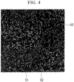
- D90 of an equivalent circle diameter of a Si phase 52 dispersed in a parent phase 51 is set in a range of 1 ⁇ m to 8 ⁇ m.
- a mold temperature in the casting may be set to 230°C or lower, and preferably 210°C or lower.
- the lower limit of the mold temperature during the casting may be 170°C, but there is no limitation thereto.
- the metal layer 13 (Cu layer 13B) and the heat sink 31 are laminated, and the resultant laminated body is put in a vacuum heating furnace and is heated therein in a pressurized state (pressure is set to 5 to 35 kgf/cm 2 (0.49 to 3.43 MPa)) in a laminating direction to subject the metal layer 13 (Cu layer 13B) and the heat sink 31 to solid-phase diffusion bonding. Furthermore, in respective bonding surfaces, which are subjected to the solid-phase diffusion bonding, of the metal layer 13 (Cu layer 13B) and the heat sink 31, scratches on the bonding surface are removed in advance and thus the bonding surfaces are made to be smooth.
- the pressure inside the vacuum heating furnace be set in a range of 10 -6 Pa to 10 -3 Pa, a heating temperature be set to 400°C to 520°C, and retention time be set in a range of 0.5 hours to 3 hours.
- the power module substrate with a heat sink 30 according to this embodiment is manufactured.
- the semiconductor element 3 is laminated on one surface (front surface) of the circuit layer 12 through a solder material, and the resultant laminated body is subjected to solder bonding in a reducing furnace.
- the power module 1 according to this embodiment is manufactured.
- the heat sink 31 constituted by an aluminum alloy, in which the Si concentration is set in a range of 1 mass% to 25 mass%, is used, and the method includes the heat sink preparing step S04 of preparing the heat sink 31 in which at the bonding surface with the metal layer 13 (Cu layer 13B), D90 of the equivalent circle diameter of the Si phase 52 dispersed in a parent phase 51 is set in a range of 1 ⁇ m to 8 ⁇ m.
- the Si phase 52 at the bonding surface, at which the Si phase comes into contact with the metal layer 13 (Cu layer 13B), is sufficiently made to be fine, and diffusion of Cu in the metal layer 13 (Cu layer 13B) is not promoted in the subsequent metal layer/heat sink bonding step S05. Accordingly, it is possible to suppress occurrence of a Kirkendall void at a bonding interface.
- D90 of the equivalent circle diameter of the Si phase 52 at the bonding surface is set in a range of 1 ⁇ m to 8 ⁇ m.
- D50 of the equivalent circle diameter of the Si phase 52 be 5 ⁇ m or less so as to reliably suppress occurrence of the Kirkendall void at the bonding interface, and it is more preferable that D50 of the equivalent circle diameter of the Si phase 52 be 3 ⁇ m or less and D90 be 6 ⁇ m or less.
- the heat sink 31 is constituted by an aluminum alloy in which the Si concentration is set in a range of 1 mass% to 25 mass%, it is possible to construct the heat sink 31 having a complicated structure provided with the flow passage 32, and thus it is possible to improve heat dissipation characteristics of the heat sink 31.
- the high-performance power module substrate since occurrence of the Kirkendall void at the bonding interface is suppressed, it is possible to construct the high-performance power module substrate with a heat sink 30 in which the bonding strength between the heat sink 31 and the metal layer 13 (Cu layer 13B) is excellent, and heat resistance is small.
- the bonding surfaces of the Cu layer 13B (copper plate 23B) and the heat sink 31 are subjected to the solid-phase diffusion bonding after scratches on the surfaces are removed in advance and the surfaces are made to be smooth. Accordingly, it is possible to suppress occurrence of the gap at the bonding interface, and thus it is possible to reliably perform the solid-phase diffusion bonding.
- the intermetallic compound layer which is formed from an intermetallic compound of Cu and Al, is formed at the bonding interface between the metal layer 13 (Cu layer 13B) and the heat sink 31, and the intermetallic compound layer has a structure in which a plurality of the intermetallic compounds are laminated along the bonding interface. Accordingly, it is possible to suppress excessive growth of the intermetallic compounds which are brittle. In addition, a volume variation on an inner side of the intermetallic compound layer decreases, and thus an internal strain is suppressed.
- oxides are dispersed in a layer shape along the bonding interface. Accordingly, an oxide film formed at the bonding surface of the heat sink 31 is reliably broken, and mutual diffusion of Cu and Al sufficiently progresses, and thus the Cu layer 13B and the heat sink 31 are reliably bonded to each other.
- FIG. 5 illustrates a heat sink 101 according to the second embodiment of the invention.
- the heat sink 101 includes a heat sink main body 110, and a copper member layer 118 that is laminated on a surface on one side (upper side in FIG. 5 ) of the heat sink main body 110 and is formed from copper or a copper alloy.
- the copper member layer 118 is constituted through bonding of a copper plate 128 constituted by a rolled plate of oxygen-free copper.
- the heat sink main body 110 is provided with a flow passage 111 through which a cooling medium flows.
- the heat sink main body 110 is constituted by an aluminum alloy in which a Si concentration is set in a range of 1 mass% to 25 mass%.
- the heat sink main body 110 is constituted by ADC3 that is a die-casting aluminum alloy defined in JIS H 2118:2006.
- ADC3 is an aluminum alloy that contains Si in a range of 9.0 to 11.0 mass%, and Mg in a range of 0.45 to 0.64 mass%.
- the Si concentration of the aluminum alloy is preferably set in a range of 10.5 mass% to 11.0 mass%, but there is no limitation to this range.
- the heat sink main body 110 and the copper member layer 118 are subjected to solid-phase diffusion bonding.
- An intermetallic compound layer is formed at a bonding interface between the heat sink main body 110 and the copper member layer 118.
- the intermetallic compound layer is formed through mutual diffusion of Al atoms of the heat sink main body 110 and Cu atoms of the copper member layer 118.
- the intermetallic compound layer has a concentration gradient in which the concentration of Al atoms further decreases, and the concentration of Cu atoms further increases as it goes toward the copper member layer 118 from the heat sink main body 110.
- the intermetallic compound layer is constituted by an intermetallic compound composed of Cu and Al.
- the intermetallic compound layer has a structure in which a plurality of the intermetallic compounds are laminated along the bonding interface.
- the thickness of the intermetallic compound layer is set in a range of 1 ⁇ m to 80 ⁇ m, and preferably in a range of 5 ⁇ m to 80 ⁇ m.
- the intermetallic compound layer has a structure in which three kinds of intermetallic compounds are laminated.
- a 0-phase and a ⁇ 2 -phase are laminated along the bonding interface between the heat sink main body 110 and the copper member layer 118, and at least one phase among a ⁇ 2 -phase, a ⁇ -phase, and a ⁇ 2 -phase is additionally laminated.
- oxides are dispersed in a layer shape along the bonding interface.
- the oxides are composed of aluminum oxides such as alumina (Al 2 O 3 ).
- the oxides are dispersed at the interface between the intermetallic compound layer and the copper member layer 118 in a disconnected state, and a region, in which the intermetallic compound layer and the copper member layer 118 are in direct contact with each other, also exists.
- the oxides may be dispersed at the inside of the ⁇ -phase, the ⁇ 2 -phase, and at least one phase among the ⁇ 2 -phase, the ⁇ -phase, and the ⁇ 2 -phase in a layer shape.
- the heat sink main body 110 to be bonded is prepared.
- D90 of the equivalent circle diameter of the Si phase dispersed in the parent phase is set in a range of 1 ⁇ m to 8 ⁇ m.
- a mold temperature in the casting may be set to 230°C or lower, and preferably 210°C or lower.
- the lower limit of the mold temperature during the casting may be 170°C, but there is no limitation thereto.
- the heat sink main body 110 and a copper plate 128 that becomes the copper member layer 118 are laminated, and the resultant laminated body is put in a vacuum heating furnace and is heated therein in a pressurized state (pressure is set to 1 to 35 kgf/cm 2 (0.10 to 3.43 MPa)) in a laminating direction to subject the copper plate 128 and the heat sink main body 110 to the solid-phase diffusion bonding. Furthermore, in respective bonding surfaces, which are subjected to the solid-phase diffusion bonding, of the copper plate 128 and the heat sink main body 110, scratches on the bonding surface are removed in advance and thus the bonding surfaces are made to be smooth.
- the pressure inside the vacuum heating furnace be set in a range of 10 -6 Pa to 10 -3 Pa, a heating temperature be set to 400°C to 520°C, and retention time be set in a range of 0.5 hours to 3 hours.
- the heat sink 101 according to this embodiment is manufactured.
- the heat sink main body 110 constituted by an aluminum alloy, in which the Si concentration is set in a range of 1 mass% to 25 mass%, is used, and the method includes the heat sink main body preparing step S101 of preparing the heat sink main body 110 in which at the bonding surface with the copper member layer 118 (copper plate 128), D90 of the equivalent circle diameter of the Si phase dispersed in the parent phase is set in a range of 1 ⁇ m to 8 ⁇ m.
- the Si phase at the bonding surface, at which the Si phase comes into contact with the copper member layer 118 (copper plate 128), is sufficiently made to be fine, and diffusion of Cu in the copper member layer 118 (copper plate 128) is not promoted. Accordingly, it is possible to suppress occurrence of a Kirkendall void at a bonding interface.
- the copper member layer 118 is formed by bonding the copper plate 128 constituted by a rolled plate of oxygen-free copper on one surface of the heat sink main body 110, and thus it is possible to make heat spread in a plane direction by the copper member layer 118, and thus it is possible to greatly improve heat dissipation characteristics.
- the heat sink main body 110 is constituted by an aluminum alloy in which the Si concentration is set in a range of 1 mass% to 25 mass%.
- the heat sink main body 110 is constituted by ADC3 (Si concentration is 9.0 to 11.0 mass%) that is a die-casting aluminum alloy defined in JIS H 2118:2006. Accordingly, it is possible to construct the heat sink main body 110 having a complicated structure provided with a flow passage and the like.
- the bonding interface between the copper member layer 118 and the heat sink main body 110 has the same configuration as that of the bonding interface between the Cu layer 13B and the heat sink 31 according to the first embodiment, it is possible to exhibit the same operational effect as in the first embodiment.
- the entirety of the metal layer may be constituted by copper or a copper alloy.
- a copper plate is bonded to a surface on the other side (lower side in FIG. 8 ) of the ceramic substrate 11 in accordance with a DBC method, an active metal brazing method, and the like, and a metal layer 213 formed from copper or a copper alloy is formed.
- the metal layer 213 and the heat sink 31 are subjected to the solid-phase diffusion bonding.
- a circuit layer 212 is also constituted by copper or a copper alloy.
- the circuit layer is formed through bonding of an aluminum plate having the purity of 99 mass% or greater, but there is no limitation thereto.
- the circuit layer may be constituted by other metals such as aluminum (4N-Al) having the purity of 99.99 mass% or greater, another aluminum or aluminum alloy, and copper or a copper alloy.
- the circuit layer may be set to have a two-layer structure of an Al layer and a Cu layer. This is also true of the power module substrate with a heat sink illustrated in FIG. 8 .
- metal layer/heat sink bonding step S05 description has been given of a configuration in which the metal layer 13 (Cu layer 13B) and the heat sink 31 are laminated, and the resultant laminated body is put in a vacuum heating furnace and is heated therein in a pressurized state in a laminating direction.
- the aluminum member 301 and the copper member 302 are laminated, and the resultant laminated body is pressurized in a laminating direction by a pair of electrodes 312 and 312 through carbon plates 311 and 311, and electrification is performed with respect to the aluminum member 301 and the copper member 302.
- the carbon plates 311 and 311, the aluminum member 301, and the copper member 302 are heated by Joule's heat, and thus the aluminum member 301 and the copper member 302 are subjected to the solid-phase diffusion bonding.
- the aluminum member 301 and the copper member 302 are directly electrically heated. Accordingly, for example, it is possible to make a temperature rising rate be as relatively fast as 30 to 100°C/min, and thus it is possible to perform the solid-phase diffusion bonding in a short time. As a result, an influence of oxidation on a bonding surface is small, and thus it is possible to perform bonding, for example, in an atmospheric atmosphere.
- a resistance value or specific heat of the aluminum member 301 and the copper member 302 it is possible to bond the aluminum member 301 and the copper member 302 in a state in which a temperature difference occurs therebetween, and thus a difference in thermal expansion decreases. As a result, it is possible to realize a reduction in a thermal stress.
- a pressurizing load that is applied by the pair of electrodes 312 and 312 be set in a range of 30 kgf/cm 2 to 100 kgf/cm 2 (2.94 MPa to 9.8 MPa).
- arithmetic average roughness Ra be set to 0.3 ⁇ m to 0.6 ⁇ m, and the maximum height Rz be set in a range of 1.3 ⁇ m to 2.3 ⁇ m.
- the surface roughness of the bonding surface be small.
- the surface roughness is preferably set in the above-described range.
- the above-described electrical heating method can be used in the metal layer/heat sink bonding step S05 according to the first embodiment.
- the ceramic substrate 11 is an insulator, it is necessary to short-circuit the carbon plates 31 1 and 311, for example, with a jig formed from carbon, and the like. Bonding conditions are the same as those in the bonding between the aluminum member 301 and the copper member 302.
- a copper plate (2 mm ⁇ 2 mm, thickness: 0.3 mm) formed from oxygen-free copper was bonded to one surface of an aluminum plate illustrated in Table 1 (10 mm ⁇ 10 mm, thickness: 3 mm) through the solid-phase diffusion bonding in accordance with the method described in the above-described embodiment.
- Example 1 to 7 and Comparative Examples 1 and 2 the aluminum plate and the copper plate were pressurized in a laminating direction with a load of 15 kgf/cm 2 (1.47 MPa), and were subjected to the solid-phase diffusion bonding in a vacuum heating furnace under conditions of 500°C for 120 minutes.
- Example 8 to 11 the aluminum plate and the copper plate were subjected to the solid-phase diffusion bonding accordance with the electrical heating method illustrated in FIG. 9 . Furthermore, in the electrodes, a pressurizing load was set to 15 kgf/cm 2 (1.47 MPa), a heating temperature (copper plate temperature) was set to 510°C, retention time at the heating temperature was set to 5 minutes, and a temperature rising rate was set to 80 °C/minute. In addition, a bonding atmosphere was set to an atmospheric atmosphere.
- FIG. 10 illustrates a measurement example of Example 2
- FIG. 11 illustrates a measurement example of Comparative Example 2.
- the obtained Si distribution image was converted into an 8-bit gray scale, thereby obtaining a Si distribution image illustrated in FIG. 10(b) and FIG. 11(b) .
- the Si distribution image was binarized as illustrated in FIG. 10(c) and FIG. 11(c) on the basis of Kapur-Sahoo-Wong (Maximum Entropy) thresholding method ( Kapur, JN; Sahoo, PK; Wong, ACK(1985), "A New Method for Gray-Le v el Picture Thresholding Using the Entropy of the Histogram", Graphical Models and Image Processing 29(3): refer to 273-285 ).
- An equivalent circle diameter (diameter) was calculated from an area (the number of pixels) in the contour on the basis of the image from which the contour of the Si phase was extracted.
- a shear test was performed by using the test piece. Furthermore, the shear test was performed on the basis of standard IEC60749-19 of International Electrotechnical Commission. An n number in the shear test was set to 30. In a Weibull plot of shear strength, an accumulative failure rate at which the shear strength becomes 100 MPa was set as a breakage rate. Furthermore, calculation of the accumulative failure rate was performed on the basis of a median rank. Evaluation results are illustrated in Table 1.
- the power module substrate with a heat sink having a structure described in the first embodiment was prepared by setting the aluminum plate illustrated in Table 1 as the heat sink.
- the configuration of the power module substrate with a heat sink is as follows. Furthermore, the solid-phase diffusion bonding between the metal layer (Cu layer) and the heat sink was performed with a vacuum heating furnace under conditions of 500°C for 120 minutes in a state in which a load in the laminating direction was set to 15 kgf/cm 2 (1.47 MPa).
- a thermal cycle for 5 minutes at -40°C and for 5 minutes at 150°C was applied to the power module substrate with a heat sink 2500 times by using a cold impact tester (TSB-51, manufactured by ESPEC CORP.) in a liquid phase (Fluorinert), and presence or absence of cracking in the ceramic substrate was evaluated by using an ultrasonic testing device. Evaluation results are illustrated in Table 1.
- Example 1 to 11 in which D90 of the Si phase at the bonding surface of the aluminum plate (heat sink) is set in the range of the invention, the breakage rate was relatively low, and occurrence of the ceramic cracking was not confirmed.
- Example 6 in which the Si concentration was set to 23.9 mass%
- Example 7 in which the Si concentration was set to 1.0 mass%, the same results were obtained.
- Examples 8 to 11 to which the electrical heating method was applied even when bonding was performed in the atmosphere, the aluminum plate and the copper plate were bonded to each other in a satisfactory manner.
- the method of manufacturing the bonded body of the invention it is possible to suppress occurrence of a Kirkendall void at the bonding interface between the aluminum member and the copper member.
- the method of manufacturing the power module substrate with a heat sink of the invention it is possible to provide a power module substrate with a heat sink in which heat resistance is small and heat dissipation is excellent.
Landscapes
- Chemical & Material Sciences (AREA)
- Engineering & Computer Science (AREA)
- Ceramic Engineering (AREA)
- Materials Engineering (AREA)
- Structural Engineering (AREA)
- Organic Chemistry (AREA)
- Mechanical Engineering (AREA)
- Cooling Or The Like Of Semiconductors Or Solid State Devices (AREA)
- Pressure Welding/Diffusion-Bonding (AREA)
- Physics & Mathematics (AREA)
- Geometry (AREA)
Abstract
Description
- The present invention relates to a method of manufacturing a bonded body that is constituted by bonding an aluminum member formed from an aluminum alloy that contains a relatively large amount of Si and a copper member that is formed from copper or a copper alloy, a method of manufacturing a power module substrate with a heat sink in which the heat sink is bonded to a power module substrate in which a circuit layer is formed on one surface of an insulating layer, and a method of manufacturing a heat sink in which a copper member layer is formed in the heat sink main body.
- Priority is claimed on Japanese Patent Application No.
2015-048151, filed on March 11, 2015 2016-025164, filed on February 12, 2016 - A semiconductor device such as an LED and a power module are provided with a structure in which a semiconductor element is bonded onto a circuit layer formed from a conductive material.
- In a large-power control power semiconductor element that is used to control wind power generation, an electric vehicle, a hybrid car, and the like, the amount of heat generation is large. According to this, as a substrate on which the power semiconductor element is mounted, for example, a power module substrate including a ceramic substrate formed from aluminum nitride (AlN), alumina (Al2O3), and the like, and a circuit layer formed by bonding a metal plate with excellent conductivity on one surface of the ceramic substrate has been widely used in the related art. Furthermore, as the power module substrate, a power module substrate in which a metal layer is formed on the other surface of the ceramic substrate is also provided.
- For example, a power module disclosed in
PTL 1 has a structure including a power module substrate in which a circuit layer and a metal layer which are formed from Al are respectively formed on one surface and the other surface of a ceramic substrate, and a semiconductor element that is bonded onto the circuit layer through a solder material. - In addition, a heat sink is bonded to a lower side of the power module substrate to radiate heat, which is transferred from the semiconductor element to the power module substrate side, to an outer side through the heat sink.
- However, as is the case with the power module described in
PTL 1, in a case where the circuit layer and the metal layer are constituted by Al, an oxide film of Al is formed on a surface, and thus it is difficult to bond the semiconductor element or the heat sink onto the surface with the solder material. - Accordingly, for example, as disclosed in
PTL 2, after a Ni plating film is formed on the surface of the circuit layer and the metal layer through electroless plating and the like, the semiconductor element or the heat sink is soldered. - In addition,
PTL 3 suggests a technology of bonding the circuit layer and the semiconductor element, and the metal layer and the heat sink, respectively, by using silver oxide paste containing a reducing agent including silver oxide particles and an organic material as an alternative of the solder material. - However, as described in
PTL 2, in the power module substrate in which the Ni plating film is formed on the surface of the circuit layer and the metal layer, during bonding of the semiconductor element and the heat sink, a surface of the Ni plating film deteriorates due to oxidation and the like, and thus there is a concern that bonding reliability of the semiconductor element and the heat sink which are bonded through the solder material deteriorates. Here, when bonding between the heat sink and the metal layer is not sufficient, there is a concern that heat resistance increases, and thus heat dissipation characteristics deteriorate. In addition, in a Ni plating step, a masking process may be performed in order to prevent problems such as electrolytic corrosion due to formation of the Ni plating in an unnecessary region occurring. As described above, in a case of performing a plating process after performing the masking process, a great deal of labor is necessary in the step of forming the Ni plating film on the surface of the circuit layer and the surface of the metal layer, and thus there is a problem in that the manufacturing cost of the power module greatly increases. - In addition, as described in
PTL 3, in a case of respectively bonding the circuit layer and the semiconductor element, and the metal layer and the heat sink by using the silver oxide paste, bondability between Al and a baked body of the silver oxide paste is poor, and thus it is necessary to form a Ag underlying layer on the surface of the circuit layer and the surface of the metal layer in advance. In a case of forming the Ag underlying layer through plating, there is a problem in that a great deal of labor is necessary similar to Ni plating. - Accordingly, PTL 4 suggests a power module substrate in which the circuit layer and the metal layer are set to have a laminated structure of an Al layer and a Cu layer. In the power module substrate, the Cu layer is disposed on the surface of the circuit layer and the metal layer, and thus it is possible to bond the semiconductor element and the heat sink by using a solder material in a satisfactory manner. As a result, heat resistance in a laminating direction decreases, and thus it is possible to transfer heat generated from the semiconductor element to the heat sink side in a satisfactory manner.
- In addition, PTL 5 suggests a power module substrate with a heat sink in which one of the metal layer and the heat sink is constituted by aluminum or an aluminum alloy, the other side is constituted by copper or a copper alloy, and the metal layer and the heat sink are subjected to solid-phase diffusion bonding. In the power module substrate with a heat sink, the metal layer and the heat sink are subjected to solid-phase diffusion bonding, and thus heat resistance is small, and heat dissipation characteristics are excellent.
-
- [PTL 1] Japanese Patent Publication No.
3171234 - [PTL 2] Japanese Unexamined Patent Application, First Publication No.
2004-172378 - [PTL 3] Japanese Unexamined Patent Application, First Publication No.
2008-208442 - [PTL 4] Japanese Unexamined Patent Application, First Publication No.
2014-160799 - [PTL 5] Japanese Unexamined Patent Application, First Publication No.
2014-099596 - However, in a heat sink having a complicated structure in which a flow passage of a cooling medium and the like are formed on an inner side, the heat sink may be manufactured by using a casted aluminum alloy that contains a relatively large amount of Si.
- Here, in a case of subjecting the aluminum member formed from a casted aluminum alloy that contains a relatively large amount of Si, and the copper member formed from copper or a copper alloy to the solid-phase diffusion bonding as described in PTL 5, it is confirmed that numerous Kirkendall voids, which occur due to unbalance of mutual diffusion, occur in the vicinity of a bonding interface. When the Kirkendall voids exist between the power module substrate and the heat sink, heat resistance increases, and thus there is a problem in that heat dissipation characteristics deteriorate.
- The invention has been made in consideration of the above-described circumstances, and an object thereof is to provide a method of manufacturing a bonded body which is capable of suppressing occurrence of a Kirkendall void at a bonding interface even in a case where an aluminum member formed from an aluminum alloy that contains a relatively large amount of Si and a copper member formed from copper or a copper alloy are subjected to solid-phase diffusion bonding, a method of manufacturing a power module substrate with a heat sink, and a method of manufacturing a heat sink.
- The present inventors have made a thorough investigation, and as a result, they obtained the following finding. It is proved that when Si and Cu come into contact with each other, diffusion of Cu is promoted when considering that Si has a melting point higher than that of Cu, and a diffusion velocity of Cu in Si is fast. According to this, when a coarse Si phase exists in an aluminum member formed from an aluminum alloy that contains a relatively large amount of Si, the Si phase and Cu in a copper member come into contact with each other at a bonding interface between the aluminum member and the copper member, and diffusion of Cu is promoted. As a result, numerous Kirkendall voids occur.
- The invention has been made on the basis of the above-described finding. According to an aspect of the invention, a method is provided for manufacturing a bonded body in which a copper member formed from copper or a copper alloy, and an aluminum member formed from an aluminum alloy in which a Si concentration is set in a range of 1 mass% to 25 mass% are bonded to each other. In the aluminum member before the bonding, D90 of an equivalent circle diameter of a Si phase at a bonding surface with the copper member is set in a range of 1 µm to 8 µm, and the aluminum member and the copper member are subjected to solid-phase diffusion bonding.
- According to the method of manufacturing a bonded body which has the above-described configuration, at the bonding surface with the copper member in the aluminum member constituted by the aluminum alloy in which the Si concentration is set in a range of 1 mass% to 25 mass%, D90 of the equivalent circle diameter of the Si phase dispersed in a parent phase is set in a range of 1 µm to 8 µm. Accordingly, the Si phase at the bonding surface, at which the Si phase comes into contact with the copper member, is sufficiently made to be fine, and diffusion of Cu in the copper member is not promoted. As a result, it is possible to suppress occurrence of a Kirkendall void at a bonding interface.
- Here, in the method of manufacturing a bonded body of the invention, it is preferable that the aluminum member and the copper member be laminated and electrically heated while being pressurized in a laminating direction to subject the aluminum member and the copper member to the solid-phase diffusion bonding.
- In this case, the aluminum member and the copper member are electrically heated while being pressurized in the laminating direction, it is possible to make a temperature rising rate fast, and thus it is possible to perform the solid-phase diffusion bonding in a relatively short time. As a result, for example, even when bonding is performed in the atmosphere, an influence of oxidation on the bonding surface is small, and thus it is possible to bond the aluminum member and the copper member in a satisfactory manner.
- According to another aspect of the invention, a method is provided for manufacturing a power module substrate with a heat sink including an insulating layer, a circuit layer that is formed on one surface of the insulating layer, a metal layer that is formed on the other surface of the insulating layer, and a heat sink that is disposed on a surface of the metal layer which is opposite to the insulating layer. A bonding surface with the heat sink in the metal layer is constituted by copper or a copper alloy, and a bonding surface with the metal layer in the heat sink is constituted by an aluminum alloy in which a Si concentration is set in a range of 1 mass% to 25 mass%. In the heat sink before the bonding, D90 of an equivalent circle diameter of a Si phase at the bonding surface with the metal layer is set in a range of 1 µm to 8 µm, and the heat sink and the metal layer are subjected to solid-phase diffusion bonding.
- According to the method of manufacturing a power module substrate with a heat sink which has the above-described configuration, at the bonding surface with the metal layer that is formed from copper or a copper alloy in the heat sink that is constituted by an aluminum alloy in which the Si concentration is set in the range of 1 mass% to 25 mass%, D90 of the equivalent circle diameter of the Si phase dispersed in a parent phase is set in a range of 1 µm to 8 µm. Accordingly, the Si phase at the bonding surface, at which the Si phase comes into contact with the metal layer, is sufficiently made to be fine, and diffusion of Cu in the metal layer is not promoted. Accordingly, it is possible to suppress occurrence of a Kirkendall void at a bonding interface. As a result, it is possible to provide a power module substrate with a heat sink in which heat resistance is small, and heat dissipation is excellent.
- In addition, in the method of manufacturing a power module substrate with a heat sink according to the aspect of the invention, the heat sink is constituted by an aluminum alloy in which the Si concentration is set in the range of 1 mass% to 25 mass%, and thus it is possible to construct the heat sink having a complicated structure provided with a flow passage and the like. As a result, it is possible to improve heat dissipation characteristics of the heat sink.
- Here, in the method of manufacturing a power module substrate with a heat sink according to the aspect of the invention, it is preferable that the heat sink and the metal layer be laminated and electrically heated while being pressurized in a laminating direction to subject the heat sink and the metal layer to the solid-phase diffusion bonding.
- In this case, the heat sink and the metal layer are electrically heated while being pressurized in the laminating direction, it is possible to make a temperature rising rate fast, and thus it is possible to perform the solid-phase diffusion bonding in a relatively short time. As a result, for example, even when bonding is performed in the atmosphere, an influence of oxidation on the bonding surface is small, and thus it is possible to bond the heat sink and the metal layer in a satisfactory manner.
- According to still another aspect of the invention, a method is provided for manufacturing a heat sink including a heat sink main body, and a copper member layer formed from copper or a copper alloy. A bonding surface with the copper member layer in the heat sink main body is constituted by an aluminum alloy in which a Si concentration is set in a range of 1 mass% to 25 mass%. In the heat sink main body before the bonding, D90 of an equivalent circle diameter of a Si phase at a bonding surface with the copper member layer is set in a range of 1 µm to 8 µm, and the heat sink main body and the copper member layer are subjected to solid-phase diffusion bonding.
- According to the method of manufacturing a heat sink which has the above-described configuration, at the bonding surface with the copper member layer that is formed from copper or a copper alloy in the heat sink main body that is constituted by an aluminum alloy in which the Si concentration is set in the range of 1 mass% to 25 mass%, D90 of the equivalent circle diameter of the Si phase dispersed in a parent phase is set in a range of 1 µm to 8 µm. Accordingly, the Si phase at the bonding surface, at which the Si phase comes into contact with the copper member layer, is sufficiently made to be fine, and diffusion of Cu in the copper member layer is not promoted. Accordingly, it is possible to suppress occurrence of a Kirkendall void at a bonding interface. As a result, it is possible to provide a heat sink in which heat resistance is small, and heat dissipation is excellent.
- In addition, the heat sink main body is constituted by an aluminum alloy in which the Si concentration is set in a range of 1 mass% to 25 mass%, and thus it is possible to construct a heat sink main body having a complicated structure provided with a flow passage and the like. In addition, the copper member layer, which is formed from copper or a copper alloy, is formed on the heat sink main body, and thus the heat sink and another member can be bonded to each other through solder and the like in a satisfactory manner. In addition, it is possible to make heat spread in a plane direction by the copper member layer, and thus it is possible to greatly improve heat dissipation characteristics.
- Here, in the method of manufacturing a heat sink of the invention, it is preferable that the heat sink main body and the copper member layer be laminated and electrically heated while being pressurized in a laminating direction to subject the heat sink main body and the copper member layer to the solid-phase diffusion bonding.
- In this case, the heat sink main body and the copper member layer are electrically heated while being pressurized in the laminating direction, it is possible to make a temperature rising rate fast, and thus it is possible to perform the solid-phase diffusion bonding in a relatively short time. As a result, for example, even when bonding is performed in the atmosphere, an influence of oxidation on the bonding surface is small, and thus it is possible to bond the heat sink main body and the copper member layer in a satisfactory manner.
- According to the invention, it is possible to provide a method of manufacturing a bonded body which is capable of suppressing occurrence of a Kirkendall void at a bonding interface even in a case where an aluminum member formed from an aluminum alloy that contains a relatively large amount of Si and a copper member formed from copper or a copper alloy are subjected to solid-phase diffusion bonding, a method of manufacturing a power module substrate with a heat sink, and a method of manufacturing a heat sink.
-
-
FIG. 1 is a schematic view illustrating a power module including a power module substrate with a heat sink according to a first embodiment of the invention. -
FIG. 2 is a flowchart illustrating a method of manufacturing the power module substrate with a heat sink according to the first embodiment, and a method of manufacturing a power module including the power module substrate with a heat sink according to the first embodiment. -
FIG. 3 is a schematic view illustrating a method of manufacturing the power module substrate according to the first embodiment, and a method of manufacturing the power module substrate with a heat sink according to the first embodiment. -
FIG. 4 is a photograph obtained by observing a structure of a bonding surface with a copper member in a heat sink before bonding in the method of manufacturing the power module substrate according to the first embodiment. -
FIG. 5 is a schematic view illustrating a heat sink according to a second embodiment of the invention. -
FIG. 6 is a flowchart illustrating a method of manufacturing the heat sink according to the second embodiment. -
FIG. 7 is a schematic view illustrating the method of manufacturing the heat sink according to the second embodiment. -
FIG. 8 is a schematic view of a power module including a power module substrate with a heat sink according to another embodiment of the invention. -
FIG. 9 is a schematic view illustrating a situation in which solid-phase diffusion bonding is performed by an electrical heating method. -
FIG. 10 is a view illustrating a sequence of measuring an equivalent circle diameter of a Si phase at a bonding surface in Example 2. -
FIG. 11 is a view illustrating a sequence of measuring the equivalent circle diameter of the Si phase at the bonding surface in Comparative Example 2. - Hereinafter, description will be given of embodiments of the invention with reference to the accompanying drawings.
-
FIG. 1 illustrates apower module 1 using a power module substrate with aheat sink 30 according to a first embodiment of the invention. - The
power module 1 includes the power module substrate with aheat sink 30, and asemiconductor element 3 that is bonded to one surface (an upper surface inFIG. 1 ) of the power module substrate with aheat sink 30 through asolder layer 2. - The power module substrate with a
heat sink 30 includes apower module substrate 10 and aheat sink 31 that is bonded to thepower module substrate 10. - The
power module substrate 10 includes aceramic substrate 11 that constitutes an insulating layer, acircuit layer 12 that is arranged on one surface (an upper surface inFIG. 1 ) of theceramic substrate 11, and ametal layer 13 that is arranged on the other surface of theceramic substrate 11. - As illustrated in
FIG. 3 , thecircuit layer 12 is formed by bonding analuminum plate 22, which is formed from aluminum or an aluminum alloy, onto one surface of theceramic substrate 11. In this embodiment, thecircuit layer 12 is formed by bonding a rolled plate (aluminum plate 22) of aluminum (2N aluminum) having the purity of 99 mass% or greater to theceramic substrate 11. Furthermore, the thickness of thealuminum plate 22, which becomes thecircuit layer 12, is set in a range of 0.1 mm to 1.0 mm, and is set to 0.6 mm in this embodiment. - As illustrated in
FIG. 1 , themetal layer 13 includes anAl layer 13A that is arranged on the other surface of theceramic substrate 11, and aCu layer 13B that is laminated on a surface of theAl layer 13A which is opposite to a surface to which theceramic substrate 11 is bonded. - As illustrated in
FIG 3 , theAl layer 13A is formed by bonding analuminum plate 23A, which is formed from aluminum or an aluminum alloy, onto the other surface of theceramic substrate 11. In this embodiment, theAl layer 13A is formed by bonding a rolled plate (aluminum plate 23A) of aluminum (2N aluminum) having the purity of 99 mass% or greater to theceramic substrate 11. The thickness of thealuminum plate 23A that is bonded to theceramic substrate 11 is set in a range of 0.1 mm to 1.0 mm, and is set to 0.6 mm in this embodiment. - The
Cu layer 13B is formed by bonding acopper plate 23B, which is formed from copper or a copper alloy, to the other surface of theAl layer 13A. In this embodiment, theCu layer 13B is formed by bonding a rolled plate (copper plate 23B) of oxygen-free copper to the other surface of theAl layer 13A. The thickness of thecopper layer 13B is set in a range of 0.1 mm to 6 mm, and is set to 1 mm in this embodiment. - The
heat sink 31 is configured to radiate heat on apower module substrate 10 side. In this embodiment, as illustrated inFIG. 1 , theheat sink 31 is provided with aflow passage 32 through which a cooling medium flows. - The
heat sink 31 is constituted by an aluminum alloy in which a Si concentration is set in a range of 1 mass% to 25 mass%. Specifically, theheat sink 31 is constituted by ADC12 that is a die-casting aluminum alloy defined in JIS H 2118:2006. Furthermore, ADC12 is an aluminum alloy that contains Cu in a range of 1.5 to 3.5 mass%, and Si in a range of 9.6 to 12.0 mass%. It is preferable that the Si concentration of the aluminum alloy be set to a range of 10.5 mass% to 12.0 mass%, but there is no limitation to the range. - Here, the
heat sink 31 and the metal layer 13 (Cu layer 13B) are subjected to solid-phase diffusion bonding. - An intermetallic compound layer is formed at a bonding interface between the metal layer 13 (
Cu layer 13B) and theheat sink 31. The intermetallic compound layer is formed through mutual diffusion of Al atoms of theheat sink 31 and Cu atoms of theCu layer 13B. The intermetallic compound layer has a concentration gradient in which the concentration of Al atoms further decreases, and the concentration of Cu atoms further increases as it goes toward theCu layer 13B from theheat sink 31. - The intermetallic compound layer is constituted by an intermetallic compound composed of Cu and Al. In this embodiment, the intermetallic compound layer has a structure in which a plurality of the intermetallic compounds are laminated along the bonding interface. Here, the thickness of the intermetallic compound layer is set in a range of 1 µm to 80 µm, and preferably in a range of 5 µm to 80 µm.
- In addition, in this embodiment, the intermetallic compound layer has a structure in which three kinds of intermetallic compounds are laminated. In the order from the
heat sink 31 side toward theCu layer 13B side, a 0-phase and a η2-phase are laminated along the bonding interface between theheat sink 31 and theCu layer 13B, and at least one phase among a ζ2-phase, a δ-phase, and a γ2-phase is laminated. - In addition, at the bonding interface between the intermetallic compound layer and the
Cu layer 13B, oxides are dispersed in a layer shape along the bonding interface. Furthermore, in this embodiment, the oxides are composed of aluminum oxides such as alumina (Al2O3). Furthermore, the oxides are dispersed at the interface between the intermetallic compound layer and theCu layer 13B in a disconnected state, and a region in which the intermetallic compound layer and theCu layer 13B are in direct contact with each other also exists. In addition, the oxides may be dispersed at the inside of the θ-phase, the η2-phase, and at least one phase among the ζ2-phase, the δ-phase, and the γ2-phase in a layer shape. - Next, description will be given of a method of manufacturing the power module substrate with a
heat sink 30 according to this embodiment with reference toFIG. 2 to FIG. 4 . - First, as illustrated in
FIG. 3 , thealuminum plate 22, which becomes thecircuit layer 12, is laminated on one surface of theceramic substrate 11 through Al-Si-basedsolder material foil 26. - In addition, the
aluminum plate 23A, which becomes theAl layer 13A, is laminated on the other surface of theceramic substrate 11 through Al-Si-basedsolder material foil 26. Furthermore, in this embodiment, as the Al-Si-basedsolder material foil 26, Al-6 mass% Si alloy foil having a thickness of 15 µm is used. - In addition, the resultant laminated body is put in a vacuum heating furnace and is heated therein in a pressurized state (pressure is set to 1 to 35 kgf/cm2 (0.10 to 3.43 MPa)) in a laminating direction to bond the
aluminum plate 22 and theceramic substrate 11, thereby forming thecircuit layer 12. In addition, theceramic substrate 11 and thealuminum plate 23A are bonded to form theAl layer 13A. - Here, it is preferable that the pressure inside the vacuum heating furnace be set in a range of 10-6 Pa to 10-3 Pa, a heating temperature be set to 600°C to 643°C, and retention time be set in a range of 30 minutes to 180 minutes.
- Next, the
copper plate 23B, which becomes theCu layer 13B, is laminated on the other surface side of theAl layer 13A. - In addition, the resultant laminated body is put in a vacuum heating furnace and is heated therein in a pressurized state (pressure is set to 3 to 35 kgf/cm2 (0.29 to 3.43 MPa)) in a laminating direction to subject the
Al layer 13A and thecopper plate 23B to solid-phase diffusion bonding, thereby forming themetal layer 13. - Here, it is preferable that the pressure inside the vacuum heating furnace be set in a range of 10-6 Pa to 10-3 Pa, a heating temperature be set to 400°C to 548°C, and retention time be set in a range of 5 minutes to 240 minutes.
- Furthermore, in respective bonding surfaces, which are subjected to the solid-phase diffusion bonding, of the
Al layer 13A and thecopper plate 23B, scratches on the bonding surface are removed in advance and thus the bonding surfaces are made to be smooth. - Next, the
heat sink 31 to be bonded is prepared. At this time, as illustrated inFIG. 4 , at a bonding surface, which is bonded to the metal layer 13 (Cu layer 13B), of theheat sink 31, D90 of an equivalent circle diameter of aSi phase 52 dispersed in aparent phase 51 is set in a range of 1 µm to 8 µm. - Here, during casting of the
heat sink 31, it is possible to control a size and a shape of theSi phase 52 at the bonding surface by adjusting a cooling rate at least in the vicinity of the bonding surface of theheat sink 31. In this case, for example, a mold temperature in the casting may be set to 230°C or lower, and preferably 210°C or lower. The lower limit of the mold temperature during the casting may be 170°C, but there is no limitation thereto. - Alternatively, it is possible to control the size and the shape of the
Si phase 52 at the bonding surface by melting at least the vicinity of the bonding surface of theheat sink 31 and rapidly cooling the vicinity. - Next, the metal layer 13 (
Cu layer 13B) and theheat sink 31 are laminated, and the resultant laminated body is put in a vacuum heating furnace and is heated therein in a pressurized state (pressure is set to 5 to 35 kgf/cm2 (0.49 to 3.43 MPa)) in a laminating direction to subject the metal layer 13 (Cu layer 13B) and theheat sink 31 to solid-phase diffusion bonding. Furthermore, in respective bonding surfaces, which are subjected to the solid-phase diffusion bonding, of the metal layer 13 (Cu layer 13B) and theheat sink 31, scratches on the bonding surface are removed in advance and thus the bonding surfaces are made to be smooth. - Here, it is preferable that the pressure inside the vacuum heating furnace be set in a range of 10-6 Pa to 10-3 Pa, a heating temperature be set to 400°C to 520°C, and retention time be set in a range of 0.5 hours to 3 hours.
- In this manner, the power module substrate with a
heat sink 30 according to this embodiment is manufactured. - Here, the
semiconductor element 3 is laminated on one surface (front surface) of thecircuit layer 12 through a solder material, and the resultant laminated body is subjected to solder bonding in a reducing furnace. - In this manner, the
power module 1 according to this embodiment is manufactured. - According to the method of manufacturing the power module substrate with a
heat sink 30, which has the above-described configuration, according to this embodiment, theheat sink 31 constituted by an aluminum alloy, in which the Si concentration is set in a range of 1 mass% to 25 mass%, is used, and the method includes the heat sink preparing step S04 of preparing theheat sink 31 in which at the bonding surface with the metal layer 13 (Cu layer 13B), D90 of the equivalent circle diameter of theSi phase 52 dispersed in aparent phase 51 is set in a range of 1 µm to 8 µm. Accordingly, theSi phase 52 at the bonding surface, at which the Si phase comes into contact with the metal layer 13 (Cu layer 13B), is sufficiently made to be fine, and diffusion of Cu in the metal layer 13 (Cu layer 13B) is not promoted in the subsequent metal layer/heat sink bonding step S05. Accordingly, it is possible to suppress occurrence of a Kirkendall void at a bonding interface. - Here, in a case where D90 of the equivalent circle diameter of the
Si phase 52 dispersed in the parent phase is less than 1 µm, the vicinity of the bonding surface of theheat sink 31 is hardened more than necessary due to precipitation hardening by a finely dispersed Si phase, and thus there is a concern that cracking may occur in theceramic substrate 11 due to a thermal stress that occurs when a heat cycle is applied to the power module substrate with aheat sink 30. - On the other hand, in a case where D90 of the equivalent circle diameter of the
Si phase 52 dispersed in the parent phase is greater than 8 µm, diffusion of Cu is promoted, and thus there is a concern that it is difficult to sufficiently suppress occurrence of the Kirkendall void at the bonding interface. - Accordingly, in this embodiment, D90 of the equivalent circle diameter of the
Si phase 52 at the bonding surface is set in a range of 1 µm to 8 µm. - Furthermore, it is preferable that D50 of the equivalent circle diameter of the
Si phase 52 be 5 µm or less so as to reliably suppress occurrence of the Kirkendall void at the bonding interface, and it is more preferable that D50 of the equivalent circle diameter of theSi phase 52 be 3 µm or less and D90 be 6 µm or less. - In addition, since the
heat sink 31 is constituted by an aluminum alloy in which the Si concentration is set in a range of 1 mass% to 25 mass%, it is possible to construct theheat sink 31 having a complicated structure provided with theflow passage 32, and thus it is possible to improve heat dissipation characteristics of theheat sink 31. - In addition, since occurrence of the Kirkendall void at the bonding interface is suppressed, it is possible to construct the high-performance power module substrate with a
heat sink 30 in which the bonding strength between theheat sink 31 and the metal layer 13 (Cu layer 13B) is excellent, and heat resistance is small. - In addition, in this embodiment, when performing the solid-phase diffusion bonding, in a case where scratches exist on the bonding surfaces, there is a concern that a gap may occur at the bonding interface. However, in this embodiment, the bonding surfaces of the
Cu layer 13B (copper plate 23B) and theheat sink 31 are subjected to the solid-phase diffusion bonding after scratches on the surfaces are removed in advance and the surfaces are made to be smooth. Accordingly, it is possible to suppress occurrence of the gap at the bonding interface, and thus it is possible to reliably perform the solid-phase diffusion bonding. - In addition, in this embodiment, the intermetallic compound layer, which is formed from an intermetallic compound of Cu and Al, is formed at the bonding interface between the metal layer 13 (
Cu layer 13B) and theheat sink 31, and the intermetallic compound layer has a structure in which a plurality of the intermetallic compounds are laminated along the bonding interface. Accordingly, it is possible to suppress excessive growth of the intermetallic compounds which are brittle. In addition, a volume variation on an inner side of the intermetallic compound layer decreases, and thus an internal strain is suppressed. - In addition, in this embodiment, at the bonding interface between the
Cu layer 13B and the intermetallic compound layer, oxides are dispersed in a layer shape along the bonding interface. Accordingly, an oxide film formed at the bonding surface of theheat sink 31 is reliably broken, and mutual diffusion of Cu and Al sufficiently progresses, and thus theCu layer 13B and theheat sink 31 are reliably bonded to each other. - Next, description will be given of a heat sink according to a second embodiment of the invention.
FIG. 5 illustrates aheat sink 101 according to the second embodiment of the invention. - The
heat sink 101 includes a heat sinkmain body 110, and acopper member layer 118 that is laminated on a surface on one side (upper side inFIG. 5 ) of the heat sinkmain body 110 and is formed from copper or a copper alloy. In this embodiment, as illustrated inFIG. 7 , thecopper member layer 118 is constituted through bonding of acopper plate 128 constituted by a rolled plate of oxygen-free copper. - The heat sink
main body 110 is provided with aflow passage 111 through which a cooling medium flows. The heat sinkmain body 110 is constituted by an aluminum alloy in which a Si concentration is set in a range of 1 mass% to 25 mass%. Specifically, the heat sinkmain body 110 is constituted by ADC3 that is a die-casting aluminum alloy defined in JIS H 2118:2006. Furthermore, ADC3 is an aluminum alloy that contains Si in a range of 9.0 to 11.0 mass%, and Mg in a range of 0.45 to 0.64 mass%. The Si concentration of the aluminum alloy is preferably set in a range of 10.5 mass% to 11.0 mass%, but there is no limitation to this range. - Here, the heat sink
main body 110 and thecopper member layer 118 are subjected to solid-phase diffusion bonding. - An intermetallic compound layer is formed at a bonding interface between the heat sink
main body 110 and thecopper member layer 118. The intermetallic compound layer is formed through mutual diffusion of Al atoms of the heat sinkmain body 110 and Cu atoms of thecopper member layer 118. The intermetallic compound layer has a concentration gradient in which the concentration of Al atoms further decreases, and the concentration of Cu atoms further increases as it goes toward thecopper member layer 118 from the heat sinkmain body 110. - The intermetallic compound layer is constituted by an intermetallic compound composed of Cu and Al. In this embodiment, the intermetallic compound layer has a structure in which a plurality of the intermetallic compounds are laminated along the bonding interface. Here, the thickness of the intermetallic compound layer is set in a range of 1 µm to 80 µm, and preferably in a range of 5 µm to 80 µm.
- In addition, in this embodiment, the intermetallic compound layer has a structure in which three kinds of intermetallic compounds are laminated. In the order from the heat sink
main body 110 side toward thecopper member layer 118 side, a 0-phase and a η2-phase are laminated along the bonding interface between the heat sinkmain body 110 and thecopper member layer 118, and at least one phase among a ζ2-phase, a δ-phase, and a γ2-phase is additionally laminated. - In addition, at the bonding interface between the intermetallic compound layer and the
copper member layer 118, oxides are dispersed in a layer shape along the bonding interface. Furthermore, in this embodiment, the oxides are composed of aluminum oxides such as alumina (Al2O3). In addition, the oxides are dispersed at the interface between the intermetallic compound layer and thecopper member layer 118 in a disconnected state, and a region, in which the intermetallic compound layer and thecopper member layer 118 are in direct contact with each other, also exists. In addition, the oxides may be dispersed at the inside of the θ-phase, the η2-phase, and at least one phase among the ζ2-phase, the δ-phase, and the γ2-phase in a layer shape. - Next, description will be given of a method of manufacturing the
heat sink 101 according to this embodiment with reference toFIG. 6 andFIG. 7 . - First, the heat sink
main body 110 to be bonded is prepared. At this time, as is the case with the heat sink 31 (refer toFIG. 4 ) described in the first embodiment, at a bonding surface with thecopper member layer 118 in the heat sinkmain body 110, D90 of the equivalent circle diameter of the Si phase dispersed in the parent phase is set in a range of 1 µm to 8 µm. - Here, when casting the heat sink
main body 110, it is possible to control a size and a shape of the Si phase at the bonding surface by adjusting a cooling rate at least in the vicinity of the bonding surface of the heat sinkmain body 110. In this case, for example, a mold temperature in the casting may be set to 230°C or lower, and preferably 210°C or lower. The lower limit of the mold temperature during the casting may be 170°C, but there is no limitation thereto. - Alternatively, it is possible to control the size and the shape of the Si phase at the bonding surface by melting at least the vicinity of the bonding surface of the heat sink
main body 110 and rapidly cooling the vicinity. - Next, as illustrated in
FIG. 7 , the heat sinkmain body 110 and acopper plate 128 that becomes thecopper member layer 118 are laminated, and the resultant laminated body is put in a vacuum heating furnace and is heated therein in a pressurized state (pressure is set to 1 to 35 kgf/cm2 (0.10 to 3.43 MPa)) in a laminating direction to subject thecopper plate 128 and the heat sinkmain body 110 to the solid-phase diffusion bonding. Furthermore, in respective bonding surfaces, which are subjected to the solid-phase diffusion bonding, of thecopper plate 128 and the heat sinkmain body 110, scratches on the bonding surface are removed in advance and thus the bonding surfaces are made to be smooth. - Here, it is preferable that the pressure inside the vacuum heating furnace be set in a range of 10-6 Pa to 10-3 Pa, a heating temperature be set to 400°C to 520°C, and retention time be set in a range of 0.5 hours to 3 hours.
- In this manner, the
heat sink 101 according to this embodiment is manufactured. - According to the method of manufacturing the
heat sink 101, which has the above-described configuration, according to this embodiment, the heat sinkmain body 110 constituted by an aluminum alloy, in which the Si concentration is set in a range of 1 mass% to 25 mass%, is used, and the method includes the heat sink main body preparing step S101 of preparing the heat sinkmain body 110 in which at the bonding surface with the copper member layer 118 (copper plate 128), D90 of the equivalent circle diameter of the Si phase dispersed in the parent phase is set in a range of 1 µm to 8 µm. Accordingly, the Si phase at the bonding surface, at which the Si phase comes into contact with the copper member layer 118 (copper plate 128), is sufficiently made to be fine, and diffusion of Cu in the copper member layer 118 (copper plate 128) is not promoted. Accordingly, it is possible to suppress occurrence of a Kirkendall void at a bonding interface. - In addition, in this embodiment, the
copper member layer 118 is formed by bonding thecopper plate 128 constituted by a rolled plate of oxygen-free copper on one surface of the heat sinkmain body 110, and thus it is possible to make heat spread in a plane direction by thecopper member layer 118, and thus it is possible to greatly improve heat dissipation characteristics. In addition, it is possible to bond another member and theheat sink 101 by using solder and the like in a satisfactory manner. - In addition, the heat sink
main body 110 is constituted by an aluminum alloy in which the Si concentration is set in a range of 1 mass% to 25 mass%. Specifically, the heat sinkmain body 110 is constituted by ADC3 (Si concentration is 9.0 to 11.0 mass%) that is a die-casting aluminum alloy defined in JIS H 2118:2006. Accordingly, it is possible to construct the heat sinkmain body 110 having a complicated structure provided with a flow passage and the like. - In addition, in this embodiment, since the bonding interface between the
copper member layer 118 and the heat sinkmain body 110 has the same configuration as that of the bonding interface between theCu layer 13B and theheat sink 31 according to the first embodiment, it is possible to exhibit the same operational effect as in the first embodiment. - Hereinbefore, description has been given of the embodiments of the invention. However, the invention is not limited thereto, and modifications can be appropriately made in a range not departing from the technical spirit of the invention.
- For example, in the first embodiment, description has been given of a configuration in which the
metal layer 13 includes theAl layer 13A and theCu layer 13B, but there is no limitation thereto. As illustrated inFIG. 8 , the entirety of the metal layer may be constituted by copper or a copper alloy. In a power module substrate with aheat sink 230 illustrated inFIG. 8 , a copper plate is bonded to a surface on the other side (lower side inFIG. 8 ) of theceramic substrate 11 in accordance with a DBC method, an active metal brazing method, and the like, and ametal layer 213 formed from copper or a copper alloy is formed. In addition, themetal layer 213 and theheat sink 31 are subjected to the solid-phase diffusion bonding. Furthermore, in thepower module substrate 210 illustrated inFIG. 8 , acircuit layer 212 is also constituted by copper or a copper alloy. - In addition, in the first embodiment, description has been given of a configuration in which the circuit layer is formed through bonding of an aluminum plate having the purity of 99 mass% or greater, but there is no limitation thereto. The circuit layer may be constituted by other metals such as aluminum (4N-Al) having the purity of 99.99 mass% or greater, another aluminum or aluminum alloy, and copper or a copper alloy. In addition, the circuit layer may be set to have a two-layer structure of an Al layer and a Cu layer. This is also true of the power module substrate with a heat sink illustrated in
FIG. 8 . - In addition, in the metal layer/heat sink bonding step S05 according to the first embodiment, description has been given of a configuration in which the metal layer 13 (
Cu layer 13B) and theheat sink 31 are laminated, and the resultant laminated body is put in a vacuum heating furnace and is heated therein in a pressurized state in a laminating direction. In addition, in the heat sink main body/copper member layer bonding step S102 according to the second embodiment, description has been given of a configuration in which the heat sinkmain body 110 and thecopper plate 128 that becomes thecopper member layer 118 are laminated, and the resultant laminated body is put in a vacuum heating furnace and is heated therein in a pressurized state (pressure of 5 to 35 kgf/cm2) in a laminating direction. However, there is no limitation to the above-described configurations, and as illustrated inFIG. 9 , an electrical heating method may be applied when subjecting an aluminum member 301 (theheat sink 31, the heat sink main body 110), and a copper member 302 (themetal layer 13, the copper member layer 118) to the solid-phase diffusion bonding. - In a case of performing the electrical heating, as illustrated in
FIG. 9 , thealuminum member 301 and thecopper member 302 are laminated, and the resultant laminated body is pressurized in a laminating direction by a pair ofelectrodes carbon plates aluminum member 301 and thecopper member 302. In this case, thecarbon plates aluminum member 301, and thecopper member 302 are heated by Joule's heat, and thus thealuminum member 301 and thecopper member 302 are subjected to the solid-phase diffusion bonding. - In the above-described electrical heating method, the
aluminum member 301 and thecopper member 302 are directly electrically heated. Accordingly, for example, it is possible to make a temperature rising rate be as relatively fast as 30 to 100°C/min, and thus it is possible to perform the solid-phase diffusion bonding in a short time. As a result, an influence of oxidation on a bonding surface is small, and thus it is possible to perform bonding, for example, in an atmospheric atmosphere. In addition, in accordance with a resistance value or specific heat of thealuminum member 301 and thecopper member 302, it is possible to bond thealuminum member 301 and thecopper member 302 in a state in which a temperature difference occurs therebetween, and thus a difference in thermal expansion decreases. As a result, it is possible to realize a reduction in a thermal stress. - Here, in the above-described electrical heating method, it is preferable that a pressurizing load that is applied by the pair of
electrodes - In addition, in a case of applying the electrical heating method, with regard to surface roughness of the
aluminum member 301 and thecopper member 302, it is preferable that arithmetic average roughness Ra be set to 0.3 µm to 0.6 µm, and the maximum height Rz be set in a range of 1.3 µm to 2.3 µm. In typical solid-phase diffusion bonding, it is preferable that the surface roughness of the bonding surface be small. However, in a case of the electrical heating method, when the surface roughness of the bonding surface is too small, interface contact resistance decreases, and thus it is difficult to locally heat the bonding interface. Accordingly, the surface roughness is preferably set in the above-described range. - Furthermore, the above-described electrical heating method can be used in the metal layer/heat sink bonding step S05 according to the first embodiment. In this case, since the
ceramic substrate 11 is an insulator, it is necessary to short-circuit thecarbon plates 31 1 and 311, for example, with a jig formed from carbon, and the like. Bonding conditions are the same as those in the bonding between thealuminum member 301 and thecopper member 302. - In addition, surface roughness of the metal layer 13 (
Cu layer 13B) and theheat sink 31 is the same as in the case of thealuminum member 301 and thecopper member 302. - Hereinafter, description will be given of results of a confirmation experiment that is performed to confirm the effect of the invention.
- A copper plate (2 mm×2 mm, thickness: 0.3 mm) formed from oxygen-free copper was bonded to one surface of an aluminum plate illustrated in Table 1 (10 mm×10 mm, thickness: 3 mm) through the solid-phase diffusion bonding in accordance with the method described in the above-described embodiment.
- In Examples 1 to 7, and Comparative Examples 1 and 2, the aluminum plate and the copper plate were pressurized in a laminating direction with a load of 15 kgf/cm2 (1.47 MPa), and were subjected to the solid-phase diffusion bonding in a vacuum heating furnace under conditions of 500°C for 120 minutes.
- In Examples 8 to 11, the aluminum plate and the copper plate were subjected to the solid-phase diffusion bonding accordance with the electrical heating method illustrated in
FIG. 9 . Furthermore, in the electrodes, a pressurizing load was set to 15 kgf/cm2 (1.47 MPa), a heating temperature (copper plate temperature) was set to 510°C, retention time at the heating temperature was set to 5 minutes, and a temperature rising rate was set to 80 °C/minute. In addition, a bonding atmosphere was set to an atmospheric atmosphere. - Before bonding, a structure observation was performed with respect to a bonding surface of the aluminum plate to measure D90 and D50 of the Si phase dispersed in the parent phase as follows. Furthermore,
FIG. 10 illustrates a measurement example of Example 2, andFIG. 11 illustrates a measurement example of Comparative Example 2. - First, surface analysis of Si was performed by using EPMA (JXA-8530F, manufactured by JEOL Ltd.) under conditions of a visual field of 360 µm, an acceleration voltage of 15 kV, and a Si contour level of 0 to 1000, thereby obtaining a Si distribution image illustrated in
FIG. 10(a) andFIG. 11(a) . - The obtained Si distribution image was converted into an 8-bit gray scale, thereby obtaining a Si distribution image illustrated in
FIG. 10(b) andFIG. 11(b) . - Next, the Si distribution image was binarized as illustrated in
FIG. 10(c) andFIG. 11(c) on the basis of Kapur-Sahoo-Wong (Maximum Entropy) thresholding method (Kapur, JN; Sahoo, PK; Wong, ACK(1985), "A New Method for Gray-Le v el Picture Thresholding Using the Entropy of the Histogram", Graphical Models and Image Processing 29(3): refer to 273-285). - Next, as illustrated in
FIG. 10(d) andFIG. 11(d) , a contour of the Si phase was extracted from the binarized image. - An equivalent circle diameter (diameter) was calculated from an area (the number of pixels) in the contour on the basis of the image from which the contour of the Si phase was extracted.
- In addition, D90 and D50 of the equivalent circle diameter that was calculated were obtained. Measurement results are illustrated in Table 1.
- A shear test was performed by using the test piece. Furthermore, the shear test was performed on the basis of standard IEC60749-19 of International Electrotechnical Commission. An n number in the shear test was set to 30. In a Weibull plot of shear strength, an accumulative failure rate at which the shear strength becomes 100 MPa was set as a breakage rate. Furthermore, calculation of the accumulative failure rate was performed on the basis of a median rank. Evaluation results are illustrated in Table 1.
- In addition, the power module substrate with a heat sink having a structure described in the first embodiment was prepared by setting the aluminum plate illustrated in Table 1 as the heat sink. The configuration of the power module substrate with a heat sink is as follows. Furthermore, the solid-phase diffusion bonding between the metal layer (Cu layer) and the heat sink was performed with a vacuum heating furnace under conditions of 500°C for 120 minutes in a state in which a load in the laminating direction was set to 15 kgf/cm2 (1.47 MPa).
- Ceramic substrate: AlN, 40 mm×40 mm, thickness: 0.635 mm
- Circuit layer: 4N aluminum, 37 mm×37 mm, thickness: 0.6 mm
- Metal layer (Al layer): 4N aluminum, 37 mm×37 mm, thickness: 0.9 mm
- Metal layer (Cu layer): Oxygen-free copper, 37 mm×37 mm, thickness: 0.3 mm
- Heat sink: aluminum alloy described in Table 1, 50 mm×50 mm, thickness: 5 mm
- A thermal cycle for 5 minutes at -40°C and for 5 minutes at 150°C was applied to the power module substrate with a heat sink 2500 times by using a cold impact tester (TSB-51, manufactured by ESPEC CORP.) in a liquid phase (Fluorinert), and presence or absence of cracking in the ceramic substrate was evaluated by using an ultrasonic testing device. Evaluation results are illustrated in Table 1.
[Table 1] Aluminum plate Equivalent circle diameter of Si phase at bonding surface Shear test Cold-hot cycle Material Si concentration (mass%) D90 (µm) D50 (µm) Breakage rate (ppm) Cracking in ceramic substrate Example 1 ADC12 11.6 1.2 0.7 5 Absent Example 2 ADC12 10.2 2.7 1.1 12 Absent Example 3 ADC12 11.6 5.2 2.6 65 Absent Example 4 ADC12 11.8 6.4 2.8 163 Absent Example 5 ADC12 10.5 7.5 4.6 274 Absent Example 6 AC9C 23.9 4.0 1.0 32 Absent Example 7 ADC6 1.0 4.0 1.1 26 Absent Example 8 ADC12 11.4 1.3 0.8 7 Absent Example 9 ADC12 10.5 7.4 4.8 248 Absent Example 10 AC9C 23.7 3.6 1.2 22 Absent Example 11 ADC6 1.0 4.1 1.2 49 Absent Comparative Example 1 ADC12 12.0 0.2 0.05 4 Present Comparative Example 2 ADC12 11.8 15 7.4 841 Absent - In Comparative Example 1 in which D90 of the Si phase at the bonding surface of the aluminum plate (heat sink) is smaller than a range of the invention, cracking occurred in the ceramic substrate. The reason for this is assumed to be because numerous fine Si particles were dispersed and thus the aluminum plate (heat sink) was hardened more than necessary.
- In Comparative Example 2 in which D90 of the Si phase at the bonding surface of the aluminum plate (heat sink) is greater than the range of the invention, the failure rate through the shear test was very high. The reason for this is assumed to be because numerous Kirkendall voids occurred at the bonding interface.
- In contrast, in Examples 1 to 11 in which D90 of the Si phase at the bonding surface of the aluminum plate (heat sink) is set in the range of the invention, the breakage rate was relatively low, and occurrence of the ceramic cracking was not confirmed. In addition, in Example 6 in which the Si concentration was set to 23.9 mass%, and Example 7 in which the Si concentration was set to 1.0 mass%, the same results were obtained. In addition, in Examples 8 to 11 to which the electrical heating method was applied, even when bonding was performed in the atmosphere, the aluminum plate and the copper plate were bonded to each other in a satisfactory manner.
- From the above-described results, according to the examples, it was confirmed that it is possible to manufacture a bonded body in which the aluminum member formed from an aluminum alloy that contains a relatively large amount of Si, and the copper member formed from copper or a copper alloy are bonded to each other in a satisfactory manner.
- According to the method of manufacturing the bonded body of the invention, it is possible to suppress occurrence of a Kirkendall void at the bonding interface between the aluminum member and the copper member. In addition, according to the method of manufacturing the power module substrate with a heat sink of the invention, it is possible to provide a power module substrate with a heat sink in which heat resistance is small and heat dissipation is excellent.
-
- 10, 210: Power module substrate
- 11: Ceramic substrate
- 13, 213: Metal layer
- 13B: Cu layer (copper member)
- 30, 230: Power module substrate with heat sink
- 31: Heat sink (aluminum member)
- 52: Si phase
- 101: Heat sink
- 110: Heat sink main body
- 118: Copper member layer
Claims (6)
- A method of manufacturing a bonded body in which a copper member formed from copper or a copper alloy, and an aluminum member formed from an aluminum alloy in which a Si concentration is set in a range of 1 mass% to 25 mass% are bonded to each other,wherein in the aluminum member before the bonding, D90 of an equivalent circle diameter of a Si phase at a bonding surface with the copper member is set in a range of 1 µm to 8 µm, andthe aluminum member and the copper member are subjected to solid-phase diffusion bonding.
- The method of manufacturing a bonded body according to Claim 1,wherein the aluminum member and the copper member are laminated and are electrically heated while being pressurized in a laminating direction to subject the aluminum member and the copper member to the solid-phase diffusion bonding.
- A method of manufacturing a power module substrate with a heat sink, the substrate including an insulating layer, a circuit layer that is formed on one surface of the insulating layer, a metal layer that is formed on the other surface of the insulating layer, and a heat sink that is disposed on a surface of the metal layer which is opposite to the insulating layer,wherein a bonding surface with the heat sink in the metal layer is constituted by copper or a copper alloy,a bonding surface with the metal layer in the heat sink is constituted by an aluminum alloy in which a Si concentration is set in a range of 1 mass% to 25 mass%,in the heat sink before the bonding, D90 of an equivalent circle diameter of a Si phase at the bonding surface with the metal layer is set in a range of 1 µm to 8 µm, andthe heat sink and the metal layer are subjected to solid-phase diffusion bonding.
- The method of manufacturing a power module substrate with a heat sink according to Claim 3,wherein the heat sink and the metal layer are laminated and are electrically heated while being pressurized in a laminating direction to subject the heat sink and the metal layer to the solid-phase diffusion bonding.
- A method of manufacturing a heat sink including a heat sink main body, and a copper member layer formed from copper or a copper alloy,wherein the heat sink main body is constituted by an aluminum alloy in which a Si concentration is set in a range of 1 mass% to 25 mass%,in the heat sink main body before the bonding, D90 of an equivalent circle diameter of a Si phase at a bonding surface with the copper member layer is set in a range of 1 µm to 8 µm, andthe heat sink main body and the copper member layer are subjected to solid-phase diffusion bonding.
- The method of manufacturing a heat sink according to Claim 5,wherein the heat sink main body and the copper member layer are laminated and are electrically heated while being pressurized in a laminating direction to subject the heat sink main body and the copper member layer to the solid-phase diffusion bonding.
Applications Claiming Priority (3)
| Application Number | Priority Date | Filing Date | Title |
|---|---|---|---|
| JP2015048151 | 2015-03-11 | ||
| JP2016025164A JP6575386B2 (en) | 2015-03-11 | 2016-02-12 | Manufacturing method of joined body, manufacturing method of power module substrate with heat sink, and manufacturing method of heat sink |
| PCT/JP2016/056409 WO2016143631A1 (en) | 2015-03-11 | 2016-03-02 | Manufacturing method for junction, manufacturing method for substrate for power module with heat sink, and manufacturing method for heat sink |
Publications (3)
| Publication Number | Publication Date |
|---|---|
| EP3269491A1 true EP3269491A1 (en) | 2018-01-17 |
| EP3269491A4 EP3269491A4 (en) | 2018-11-14 |
| EP3269491B1 EP3269491B1 (en) | 2019-11-27 |
Family
ID=56982963
Family Applications (1)
| Application Number | Title | Priority Date | Filing Date |
|---|---|---|---|
| EP16761601.0A Active EP3269491B1 (en) | 2015-03-11 | 2016-03-02 | Manufacturing method for junction, manufacturing method for substrate for power module with heat sink, and manufacturing method for heat sink |
Country Status (5)
| Country | Link |
|---|---|
| US (1) | US20180040533A1 (en) |
| EP (1) | EP3269491B1 (en) |
| JP (1) | JP6575386B2 (en) |
| KR (1) | KR20170126878A (en) |
| CN (1) | CN107427954B (en) |
Cited By (3)
| Publication number | Priority date | Publication date | Assignee | Title |
|---|---|---|---|---|
| EP3355370A4 (en) * | 2015-09-25 | 2019-05-01 | Mitsubishi Materials Corporation | SUBSTRATE FOR LUMINESCENT MODULE, LUMINESCENT MODULE, SUBSTRATE FOR LUMINESCENT MODULE WITH COOLER, AND METHOD FOR MANUFACTURING SUBSTRATE FOR LUMINESCENT MODULE |
| EP3703116A4 (en) * | 2017-10-27 | 2021-07-21 | Mitsubishi Materials Corporation | BOUND BODY, INSULATED CIRCUIT BOARD WITH HEAT SINK, AND HEAT SINK |
| EP3770950A4 (en) * | 2018-03-23 | 2022-02-16 | Mitsubishi Materials Corporation | METHOD FOR MANUFACTURING MODULE MOUNTED ON ELECTRONIC COMPONENT |
Families Citing this family (5)
| Publication number | Priority date | Publication date | Assignee | Title |
|---|---|---|---|---|
| WO2019188885A1 (en) * | 2018-03-26 | 2019-10-03 | 三菱マテリアル株式会社 | Method of manufacturing bonded body for insulating circuit board, and bonded body for insulating circuit board |
| CN112823073B (en) * | 2018-11-28 | 2022-07-05 | 三菱综合材料株式会社 | Joined body, insulated circuit board with heat sink, and heat sink |
| KR102887437B1 (en) * | 2018-12-21 | 2025-11-17 | 닛폰 하츠죠 가부시키가이샤 | Joining method and joint body |
| JP7659377B2 (en) * | 2020-09-15 | 2025-04-09 | Dowaメタルテック株式会社 | Heat dissipation member and manufacturing method thereof |
| KR102897765B1 (en) * | 2022-12-13 | 2025-12-10 | 주식회사 케이씨씨 | Preparing method for ceramic substrate |
Family Cites Families (6)
| Publication number | Priority date | Publication date | Assignee | Title |
|---|---|---|---|---|
| JPH06226468A (en) * | 1993-02-05 | 1994-08-16 | Suzuki Motor Corp | Solid state diffusion joining method |
| WO2011155379A1 (en) * | 2010-06-08 | 2011-12-15 | 株式会社Neomaxマテリアル | Aluminum copper clad material |
| JP6426883B2 (en) * | 2011-11-28 | 2018-11-21 | 株式会社Uacj | Method of manufacturing joined body excellent in corrosion resistance |
| JP5403129B2 (en) * | 2012-03-30 | 2014-01-29 | 三菱マテリアル株式会社 | Power module substrate, power module substrate with heat sink, power module, and method for manufacturing power module substrate |
| JP5892046B2 (en) * | 2012-11-15 | 2016-03-23 | 株式会社オートネットワーク技術研究所 | Connection structure and connection structure |
| WO2014184880A1 (en) * | 2013-05-14 | 2014-11-20 | 株式会社Uacj | Aluminum alloy material, single layer of which allows thermal bonding; manufacturing method therefor; and aluminum bonded body using said aluminum alloy material |
-
2016
- 2016-02-12 JP JP2016025164A patent/JP6575386B2/en active Active
- 2016-03-02 EP EP16761601.0A patent/EP3269491B1/en active Active
- 2016-03-02 CN CN201680015032.6A patent/CN107427954B/en active Active
- 2016-03-02 KR KR1020177023692A patent/KR20170126878A/en not_active Withdrawn
- 2016-03-02 US US15/557,208 patent/US20180040533A1/en not_active Abandoned
Cited By (5)
| Publication number | Priority date | Publication date | Assignee | Title |
|---|---|---|---|---|
| EP3355370A4 (en) * | 2015-09-25 | 2019-05-01 | Mitsubishi Materials Corporation | SUBSTRATE FOR LUMINESCENT MODULE, LUMINESCENT MODULE, SUBSTRATE FOR LUMINESCENT MODULE WITH COOLER, AND METHOD FOR MANUFACTURING SUBSTRATE FOR LUMINESCENT MODULE |
| EP3703116A4 (en) * | 2017-10-27 | 2021-07-21 | Mitsubishi Materials Corporation | BOUND BODY, INSULATED CIRCUIT BOARD WITH HEAT SINK, AND HEAT SINK |
| US11094606B2 (en) | 2017-10-27 | 2021-08-17 | Mitsubishi Materials Corporation | Bonded body, insulated circuit board with heat sink, and heat sink |
| EP3770950A4 (en) * | 2018-03-23 | 2022-02-16 | Mitsubishi Materials Corporation | METHOD FOR MANUFACTURING MODULE MOUNTED ON ELECTRONIC COMPONENT |
| US11476127B2 (en) | 2018-03-23 | 2022-10-18 | Mitsubishi Materials Corporation | Manufacturing method of electronic-component-mounted module |
Also Published As
| Publication number | Publication date |
|---|---|
| US20180040533A1 (en) | 2018-02-08 |
| JP2016168625A (en) | 2016-09-23 |
| CN107427954A (en) | 2017-12-01 |
| JP6575386B2 (en) | 2019-09-18 |
| EP3269491A4 (en) | 2018-11-14 |
| EP3269491B1 (en) | 2019-11-27 |
| KR20170126878A (en) | 2017-11-20 |
| CN107427954B (en) | 2020-01-03 |
Similar Documents
| Publication | Publication Date | Title |
|---|---|---|
| EP3285292B1 (en) | Bonded body, substrate for power module with heat sink, heat sink, method for producing bonded body, method for producing substrate for power module with heat sink, and method for producing heat sink | |
| EP3269491B1 (en) | Manufacturing method for junction, manufacturing method for substrate for power module with heat sink, and manufacturing method for heat sink | |
| EP3285291B1 (en) | Bonded body, substrate for power module with heat sink, heat sink, method for producing bonded body, method for producing substrate for power module with heat sink, and method for producing heat sink | |
| EP3196929B1 (en) | Method of manufacturing bonded body, method of manufacturing power module substrate with heat sink, and method of manufacturing heat sink | |
| EP2940719B1 (en) | Power module | |
| EP3196930B1 (en) | Bonded body, power module substrate with heat sink, use of the bonded body as a heat sink, method for manufacturing bonded body | |
| EP3279936B1 (en) | Method for manufacturing substrate for power module with heat sink | |
| JP5866075B2 (en) | Bonding material manufacturing method, bonding method, and power semiconductor device | |
| US10497585B2 (en) | Bonded body, substrate for power module with heat sink, heat sink, method for producing bonded body, method for producing substrate for power module with heat sink, and method for producing heat sink | |
| US20170141010A1 (en) | Method for producing ceramic-aluminum bonded body, method for producing power module substrate, ceramic-aluminum bonded body, and power module substrate | |
| WO2016167218A1 (en) | Bonded body, substrate for power module with heat sink, heat sink, method for producing bonded body, method for producing substrate for power module with heat sink, and method for producing heat sink | |
| TWI753854B (en) | Method of producing bonded body, method of producing power module substrate with heat sink and method of producing heat sink |
Legal Events
| Date | Code | Title | Description |
|---|---|---|---|
| STAA | Information on the status of an ep patent application or granted ep patent |
Free format text: STATUS: THE INTERNATIONAL PUBLICATION HAS BEEN MADE |
|
| PUAI | Public reference made under article 153(3) epc to a published international application that has entered the european phase |
Free format text: ORIGINAL CODE: 0009012 |
|
| STAA | Information on the status of an ep patent application or granted ep patent |
Free format text: STATUS: REQUEST FOR EXAMINATION WAS MADE |
|
| 17P | Request for examination filed |
Effective date: 20170914 |
|
| AK | Designated contracting states |
Kind code of ref document: A1 Designated state(s): AL AT BE BG CH CY CZ DE DK EE ES FI FR GB GR HR HU IE IS IT LI LT LU LV MC MK MT NL NO PL PT RO RS SE SI SK SM TR |
|
| AX | Request for extension of the european patent |
Extension state: BA ME |
|
| DAV | Request for validation of the european patent (deleted) | ||
| DAX | Request for extension of the european patent (deleted) | ||
| A4 | Supplementary search report drawn up and despatched |
Effective date: 20181011 |
|
| RIC1 | Information provided on ipc code assigned before grant |
Ipc: H01L 21/48 20060101ALI20181005BHEP Ipc: H01L 23/40 20060101ALI20181005BHEP Ipc: B23K 1/00 20060101ALI20181005BHEP Ipc: H01L 23/473 20060101ALN20181005BHEP Ipc: H01L 33/64 20100101ALN20181005BHEP Ipc: B23K 101/40 20060101ALI20181005BHEP Ipc: B23K 20/00 20060101AFI20181005BHEP Ipc: C04B 37/02 20060101ALI20181005BHEP Ipc: H01L 23/373 20060101ALI20181005BHEP |
|
| GRAP | Despatch of communication of intention to grant a patent |
Free format text: ORIGINAL CODE: EPIDOSNIGR1 |
|
| STAA | Information on the status of an ep patent application or granted ep patent |
Free format text: STATUS: GRANT OF PATENT IS INTENDED |
|
| RIC1 | Information provided on ipc code assigned before grant |
Ipc: B23K 103/10 20060101ALN20190619BHEP Ipc: B23K 103/12 20060101ALN20190619BHEP Ipc: H01L 23/473 20060101ALN20190619BHEP Ipc: H01L 33/64 20100101ALN20190619BHEP Ipc: B23K 103/18 20060101ALN20190619BHEP Ipc: H01L 21/48 20060101ALI20190619BHEP Ipc: B23K 101/40 20060101ALI20190619BHEP Ipc: H01L 23/40 20060101ALI20190619BHEP Ipc: B23K 1/00 20060101ALI20190619BHEP Ipc: H01L 23/373 20060101ALI20190619BHEP Ipc: C04B 37/02 20060101ALI20190619BHEP Ipc: B23K 11/20 20060101ALI20190619BHEP Ipc: B23K 20/00 20060101AFI20190619BHEP |
|
| RAP1 | Party data changed (applicant data changed or rights of an application transferred) |
Owner name: MITSUBISHI MATERIALS CORPORATION |
|
| RIC1 | Information provided on ipc code assigned before grant |
Ipc: H01L 23/40 20060101ALI20190702BHEP Ipc: H01L 23/373 20060101ALI20190702BHEP Ipc: H01L 21/48 20060101ALI20190702BHEP Ipc: H01L 33/64 20100101ALN20190702BHEP Ipc: B23K 20/00 20060101AFI20190702BHEP Ipc: C04B 37/02 20060101ALI20190702BHEP Ipc: B23K 103/10 20060101ALN20190702BHEP Ipc: H01L 23/473 20060101ALN20190702BHEP Ipc: B23K 103/18 20060101ALN20190702BHEP Ipc: B23K 1/00 20060101ALI20190702BHEP Ipc: B23K 11/20 20060101ALI20190702BHEP Ipc: B23K 103/12 20060101ALN20190702BHEP Ipc: B23K 101/40 20060101ALI20190702BHEP |
|
| INTG | Intention to grant announced |
Effective date: 20190719 |
|
| GRAS | Grant fee paid |
Free format text: ORIGINAL CODE: EPIDOSNIGR3 |
|
| GRAA | (expected) grant |
Free format text: ORIGINAL CODE: 0009210 |
|
| STAA | Information on the status of an ep patent application or granted ep patent |
Free format text: STATUS: THE PATENT HAS BEEN GRANTED |
|
| AK | Designated contracting states |
Kind code of ref document: B1 Designated state(s): AL AT BE BG CH CY CZ DE DK EE ES FI FR GB GR HR HU IE IS IT LI LT LU LV MC MK MT NL NO PL PT RO RS SE SI SK SM TR |
|
| REG | Reference to a national code |
Ref country code: GB Ref legal event code: FG4D |
|
| REG | Reference to a national code |
Ref country code: CH Ref legal event code: EP |
|
| REG | Reference to a national code |
Ref country code: AT Ref legal event code: REF Ref document number: 1206139 Country of ref document: AT Kind code of ref document: T Effective date: 20191215 |
|
| REG | Reference to a national code |
Ref country code: DE Ref legal event code: R096 Ref document number: 602016025151 Country of ref document: DE |
|
| REG | Reference to a national code |
Ref country code: IE Ref legal event code: FG4D |
|
| REG | Reference to a national code |
Ref country code: NL Ref legal event code: MP Effective date: 20191127 |
|
| REG | Reference to a national code |
Ref country code: LT Ref legal event code: MG4D |
|
| PG25 | Lapsed in a contracting state [announced via postgrant information from national office to epo] |
Ref country code: GR Free format text: LAPSE BECAUSE OF FAILURE TO SUBMIT A TRANSLATION OF THE DESCRIPTION OR TO PAY THE FEE WITHIN THE PRESCRIBED TIME-LIMIT Effective date: 20200228 Ref country code: NO Free format text: LAPSE BECAUSE OF FAILURE TO SUBMIT A TRANSLATION OF THE DESCRIPTION OR TO PAY THE FEE WITHIN THE PRESCRIBED TIME-LIMIT Effective date: 20200227 Ref country code: LT Free format text: LAPSE BECAUSE OF FAILURE TO SUBMIT A TRANSLATION OF THE DESCRIPTION OR TO PAY THE FEE WITHIN THE PRESCRIBED TIME-LIMIT Effective date: 20191127 Ref country code: NL Free format text: LAPSE BECAUSE OF FAILURE TO SUBMIT A TRANSLATION OF THE DESCRIPTION OR TO PAY THE FEE WITHIN THE PRESCRIBED TIME-LIMIT Effective date: 20191127 Ref country code: SE Free format text: LAPSE BECAUSE OF FAILURE TO SUBMIT A TRANSLATION OF THE DESCRIPTION OR TO PAY THE FEE WITHIN THE PRESCRIBED TIME-LIMIT Effective date: 20191127 Ref country code: LV Free format text: LAPSE BECAUSE OF FAILURE TO SUBMIT A TRANSLATION OF THE DESCRIPTION OR TO PAY THE FEE WITHIN THE PRESCRIBED TIME-LIMIT Effective date: 20191127 Ref country code: BG Free format text: LAPSE BECAUSE OF FAILURE TO SUBMIT A TRANSLATION OF THE DESCRIPTION OR TO PAY THE FEE WITHIN THE PRESCRIBED TIME-LIMIT Effective date: 20200227 Ref country code: FI Free format text: LAPSE BECAUSE OF FAILURE TO SUBMIT A TRANSLATION OF THE DESCRIPTION OR TO PAY THE FEE WITHIN THE PRESCRIBED TIME-LIMIT Effective date: 20191127 |
|
| PG25 | Lapsed in a contracting state [announced via postgrant information from national office to epo] |
Ref country code: IS Free format text: LAPSE BECAUSE OF FAILURE TO SUBMIT A TRANSLATION OF THE DESCRIPTION OR TO PAY THE FEE WITHIN THE PRESCRIBED TIME-LIMIT Effective date: 20200327 Ref country code: RS Free format text: LAPSE BECAUSE OF FAILURE TO SUBMIT A TRANSLATION OF THE DESCRIPTION OR TO PAY THE FEE WITHIN THE PRESCRIBED TIME-LIMIT Effective date: 20191127 Ref country code: HR Free format text: LAPSE BECAUSE OF FAILURE TO SUBMIT A TRANSLATION OF THE DESCRIPTION OR TO PAY THE FEE WITHIN THE PRESCRIBED TIME-LIMIT Effective date: 20191127 |
|
| PG25 | Lapsed in a contracting state [announced via postgrant information from national office to epo] |
Ref country code: AL Free format text: LAPSE BECAUSE OF FAILURE TO SUBMIT A TRANSLATION OF THE DESCRIPTION OR TO PAY THE FEE WITHIN THE PRESCRIBED TIME-LIMIT Effective date: 20191127 |
|
| PG25 | Lapsed in a contracting state [announced via postgrant information from national office to epo] |
Ref country code: ES Free format text: LAPSE BECAUSE OF FAILURE TO SUBMIT A TRANSLATION OF THE DESCRIPTION OR TO PAY THE FEE WITHIN THE PRESCRIBED TIME-LIMIT Effective date: 20191127 Ref country code: DK Free format text: LAPSE BECAUSE OF FAILURE TO SUBMIT A TRANSLATION OF THE DESCRIPTION OR TO PAY THE FEE WITHIN THE PRESCRIBED TIME-LIMIT Effective date: 20191127 Ref country code: RO Free format text: LAPSE BECAUSE OF FAILURE TO SUBMIT A TRANSLATION OF THE DESCRIPTION OR TO PAY THE FEE WITHIN THE PRESCRIBED TIME-LIMIT Effective date: 20191127 Ref country code: CZ Free format text: LAPSE BECAUSE OF FAILURE TO SUBMIT A TRANSLATION OF THE DESCRIPTION OR TO PAY THE FEE WITHIN THE PRESCRIBED TIME-LIMIT Effective date: 20191127 Ref country code: PT Free format text: LAPSE BECAUSE OF FAILURE TO SUBMIT A TRANSLATION OF THE DESCRIPTION OR TO PAY THE FEE WITHIN THE PRESCRIBED TIME-LIMIT Effective date: 20200419 Ref country code: EE Free format text: LAPSE BECAUSE OF FAILURE TO SUBMIT A TRANSLATION OF THE DESCRIPTION OR TO PAY THE FEE WITHIN THE PRESCRIBED TIME-LIMIT Effective date: 20191127 |
|
| REG | Reference to a national code |
Ref country code: DE Ref legal event code: R097 Ref document number: 602016025151 Country of ref document: DE |
|
| PG25 | Lapsed in a contracting state [announced via postgrant information from national office to epo] |
Ref country code: SK Free format text: LAPSE BECAUSE OF FAILURE TO SUBMIT A TRANSLATION OF THE DESCRIPTION OR TO PAY THE FEE WITHIN THE PRESCRIBED TIME-LIMIT Effective date: 20191127 Ref country code: SM Free format text: LAPSE BECAUSE OF FAILURE TO SUBMIT A TRANSLATION OF THE DESCRIPTION OR TO PAY THE FEE WITHIN THE PRESCRIBED TIME-LIMIT Effective date: 20191127 |
|
| REG | Reference to a national code |
Ref country code: AT Ref legal event code: MK05 Ref document number: 1206139 Country of ref document: AT Kind code of ref document: T Effective date: 20191127 |
|
| PLBE | No opposition filed within time limit |
Free format text: ORIGINAL CODE: 0009261 |
|
| STAA | Information on the status of an ep patent application or granted ep patent |
Free format text: STATUS: NO OPPOSITION FILED WITHIN TIME LIMIT |
|
| PG25 | Lapsed in a contracting state [announced via postgrant information from national office to epo] |
Ref country code: MC Free format text: LAPSE BECAUSE OF FAILURE TO SUBMIT A TRANSLATION OF THE DESCRIPTION OR TO PAY THE FEE WITHIN THE PRESCRIBED TIME-LIMIT Effective date: 20191127 |
|
| REG | Reference to a national code |
Ref country code: CH Ref legal event code: PL |
|
| 26N | No opposition filed |
Effective date: 20200828 |
|
| PG25 | Lapsed in a contracting state [announced via postgrant information from national office to epo] |
Ref country code: SI Free format text: LAPSE BECAUSE OF FAILURE TO SUBMIT A TRANSLATION OF THE DESCRIPTION OR TO PAY THE FEE WITHIN THE PRESCRIBED TIME-LIMIT Effective date: 20191127 Ref country code: PL Free format text: LAPSE BECAUSE OF FAILURE TO SUBMIT A TRANSLATION OF THE DESCRIPTION OR TO PAY THE FEE WITHIN THE PRESCRIBED TIME-LIMIT Effective date: 20191127 Ref country code: AT Free format text: LAPSE BECAUSE OF FAILURE TO SUBMIT A TRANSLATION OF THE DESCRIPTION OR TO PAY THE FEE WITHIN THE PRESCRIBED TIME-LIMIT Effective date: 20191127 |
|
| REG | Reference to a national code |
Ref country code: BE Ref legal event code: MM Effective date: 20200331 |
|
| PG25 | Lapsed in a contracting state [announced via postgrant information from national office to epo] |
Ref country code: LU Free format text: LAPSE BECAUSE OF NON-PAYMENT OF DUE FEES Effective date: 20200302 |
|
| PG25 | Lapsed in a contracting state [announced via postgrant information from national office to epo] |
Ref country code: IE Free format text: LAPSE BECAUSE OF NON-PAYMENT OF DUE FEES Effective date: 20200302 Ref country code: CH Free format text: LAPSE BECAUSE OF NON-PAYMENT OF DUE FEES Effective date: 20200331 Ref country code: LI Free format text: LAPSE BECAUSE OF NON-PAYMENT OF DUE FEES Effective date: 20200331 |
|
| PG25 | Lapsed in a contracting state [announced via postgrant information from national office to epo] |
Ref country code: BE Free format text: LAPSE BECAUSE OF NON-PAYMENT OF DUE FEES Effective date: 20200331 |
|
| PG25 | Lapsed in a contracting state [announced via postgrant information from national office to epo] |
Ref country code: TR Free format text: LAPSE BECAUSE OF FAILURE TO SUBMIT A TRANSLATION OF THE DESCRIPTION OR TO PAY THE FEE WITHIN THE PRESCRIBED TIME-LIMIT Effective date: 20191127 Ref country code: MT Free format text: LAPSE BECAUSE OF FAILURE TO SUBMIT A TRANSLATION OF THE DESCRIPTION OR TO PAY THE FEE WITHIN THE PRESCRIBED TIME-LIMIT Effective date: 20191127 Ref country code: CY Free format text: LAPSE BECAUSE OF FAILURE TO SUBMIT A TRANSLATION OF THE DESCRIPTION OR TO PAY THE FEE WITHIN THE PRESCRIBED TIME-LIMIT Effective date: 20191127 |
|
| PG25 | Lapsed in a contracting state [announced via postgrant information from national office to epo] |
Ref country code: MK Free format text: LAPSE BECAUSE OF FAILURE TO SUBMIT A TRANSLATION OF THE DESCRIPTION OR TO PAY THE FEE WITHIN THE PRESCRIBED TIME-LIMIT Effective date: 20191127 |
|
| PGFP | Annual fee paid to national office [announced via postgrant information from national office to epo] |
Ref country code: GB Payment date: 20240320 Year of fee payment: 9 |
|
| PGFP | Annual fee paid to national office [announced via postgrant information from national office to epo] |
Ref country code: IT Payment date: 20240329 Year of fee payment: 9 Ref country code: FR Payment date: 20240328 Year of fee payment: 9 |
|
| GBPC | Gb: european patent ceased through non-payment of renewal fee |
Effective date: 20250302 |
|
| PG25 | Lapsed in a contracting state [announced via postgrant information from national office to epo] |
Ref country code: GB Free format text: LAPSE BECAUSE OF NON-PAYMENT OF DUE FEES Effective date: 20250302 |
|
| PG25 | Lapsed in a contracting state [announced via postgrant information from national office to epo] |
Ref country code: FR Free format text: LAPSE BECAUSE OF NON-PAYMENT OF DUE FEES Effective date: 20250331 Ref country code: IT Free format text: LAPSE BECAUSE OF NON-PAYMENT OF DUE FEES Effective date: 20250302 |
|
| PGFP | Annual fee paid to national office [announced via postgrant information from national office to epo] |
Ref country code: DE Payment date: 20260319 Year of fee payment: 11 |