EP3267616A1 - Wireless communication system, base station, and terminal - Google Patents
Wireless communication system, base station, and terminal Download PDFInfo
- Publication number
- EP3267616A1 EP3267616A1 EP17178657.7A EP17178657A EP3267616A1 EP 3267616 A1 EP3267616 A1 EP 3267616A1 EP 17178657 A EP17178657 A EP 17178657A EP 3267616 A1 EP3267616 A1 EP 3267616A1
- Authority
- EP
- European Patent Office
- Prior art keywords
- signal
- base station
- time period
- terminal
- enb3
- Prior art date
- Legal status (The legal status is an assumption and is not a legal conclusion. Google has not performed a legal analysis and makes no representation as to the accuracy of the status listed.)
- Granted
Links
Images





Classifications
-
- H—ELECTRICITY
- H04—ELECTRIC COMMUNICATION TECHNIQUE
- H04L—TRANSMISSION OF DIGITAL INFORMATION, e.g. TELEGRAPHIC COMMUNICATION
- H04L5/00—Arrangements affording multiple use of the transmission path
- H04L5/003—Arrangements for allocating sub-channels of the transmission path
- H04L5/0048—Allocation of pilot signals, i.e. of signals known to the receiver
-
- H—ELECTRICITY
- H04—ELECTRIC COMMUNICATION TECHNIQUE
- H04W—WIRELESS COMMUNICATION NETWORKS
- H04W72/00—Local resource management
- H04W72/04—Wireless resource allocation
- H04W72/044—Wireless resource allocation based on the type of the allocated resource
- H04W72/0446—Resources in time domain, e.g. slots or frames
-
- H—ELECTRICITY
- H04—ELECTRIC COMMUNICATION TECHNIQUE
- H04B—TRANSMISSION
- H04B17/00—Monitoring; Testing
- H04B17/10—Monitoring; Testing of transmitters
- H04B17/11—Monitoring; Testing of transmitters for calibration
- H04B17/12—Monitoring; Testing of transmitters for calibration of transmit antennas, e.g. of the amplitude or phase
-
- H—ELECTRICITY
- H04—ELECTRIC COMMUNICATION TECHNIQUE
- H04L—TRANSMISSION OF DIGITAL INFORMATION, e.g. TELEGRAPHIC COMMUNICATION
- H04L27/00—Modulated-carrier systems
- H04L27/26—Systems using multi-frequency codes
- H04L27/2601—Multicarrier modulation systems
- H04L27/2602—Signal structure
- H04L27/2605—Symbol extensions, e.g. Zero Tail, Unique Word [UW]
-
- H—ELECTRICITY
- H04—ELECTRIC COMMUNICATION TECHNIQUE
- H04L—TRANSMISSION OF DIGITAL INFORMATION, e.g. TELEGRAPHIC COMMUNICATION
- H04L5/00—Arrangements affording multiple use of the transmission path
- H04L5/0091—Signalling for the administration of the divided path, e.g. signalling of configuration information
- H04L5/0094—Indication of how sub-channels of the path are allocated
-
- H—ELECTRICITY
- H04—ELECTRIC COMMUNICATION TECHNIQUE
- H04L—TRANSMISSION OF DIGITAL INFORMATION, e.g. TELEGRAPHIC COMMUNICATION
- H04L5/00—Arrangements affording multiple use of the transmission path
- H04L5/14—Two-way operation using the same type of signal, i.e. duplex
-
- H—ELECTRICITY
- H04—ELECTRIC COMMUNICATION TECHNIQUE
- H04W—WIRELESS COMMUNICATION NETWORKS
- H04W28/00—Network traffic management; Network resource management
- H04W28/02—Traffic management, e.g. flow control or congestion control
- H04W28/06—Optimizing the usage of the radio link, e.g. header compression, information sizing, discarding information
-
- H—ELECTRICITY
- H04—ELECTRIC COMMUNICATION TECHNIQUE
- H04W—WIRELESS COMMUNICATION NETWORKS
- H04W72/00—Local resource management
- H04W72/20—Control channels or signalling for resource management
- H04W72/21—Control channels or signalling for resource management in the uplink direction of a wireless link, i.e. towards the network
-
- H—ELECTRICITY
- H04—ELECTRIC COMMUNICATION TECHNIQUE
- H04J—MULTIPLEX COMMUNICATION
- H04J11/00—Orthogonal multiplex systems, e.g. using WALSH codes
- H04J2011/0003—Combination with other multiplexing techniques
- H04J2011/0013—Combination with other multiplexing techniques with TDM/TDMA
-
- H—ELECTRICITY
- H04—ELECTRIC COMMUNICATION TECHNIQUE
- H04L—TRANSMISSION OF DIGITAL INFORMATION, e.g. TELEGRAPHIC COMMUNICATION
- H04L5/00—Arrangements affording multiple use of the transmission path
- H04L5/0001—Arrangements for dividing the transmission path
- H04L5/0003—Two-dimensional division
- H04L5/0005—Time-frequency
- H04L5/0007—Time-frequency the frequencies being orthogonal, e.g. OFDM(A) or DMT
- H04L5/001—Time-frequency the frequencies being orthogonal, e.g. OFDM(A) or DMT the frequencies being arranged in component carriers
-
- H—ELECTRICITY
- H04—ELECTRIC COMMUNICATION TECHNIQUE
- H04L—TRANSMISSION OF DIGITAL INFORMATION, e.g. TELEGRAPHIC COMMUNICATION
- H04L5/00—Arrangements affording multiple use of the transmission path
- H04L5/003—Arrangements for allocating sub-channels of the transmission path
- H04L5/0058—Allocation criteria
- H04L5/006—Quality of the received signal, e.g. BER, SNR, water filling
Definitions
- the embodiments discussed herein are related to a wireless communication system, a base station, and a terminal.
- a time-division duplex (TDD) under the same frequency may be applied to wireless communications between a base station and a terminal.
- TDD time-division duplex
- GP guard period
- DL downlink
- UL uplink
- the base station transmits a certain predetermined signal in the GP.
- An example of the predetermined signal transmitted in the GP may be some kind of test signal such as a calibration signal.
- the predetermined signal may be considered as "a signal which is not directed for the terminal".
- the GP may become insufficient depending on a period during which the base station tries to transmit the predetermined signal.
- the GP may become insufficient.
- wireless resources available for terminals are reduced, and the utilization efficiency of the wireless resources may decrease.
- one of the objects of the techniques described herein is to achieve compatibility between a transmission of the predetermined signal by the base station and a suppression of reduction in the utilization efficiency of the wireless resources in the wireless communication system of TDD.
- a wireless communication system may include a terminal and a base station.
- the base station may selectively apply one of a first time period having a first guard period and a second time period having a second guard period to time-division duplex communication with a terminal.
- the base station may notify the terminal of information related to a timing of selectively applying one of the first time period and the second time period, and transmit a predetermined signal in the first guard period.
- a base station may include a controller and a communication circuitry.
- the controller may selectively apply one of a first time period having a first guard period and a second time period having a second guard period to time-division duplex communication with a terminal.
- the communication circuitry may notify the terminal of information related to a timing of selectively applying one of the first time period and the second time period, and transmit a predetermined signal in the first guard period.
- a terminal configured to wirelessly communicate with a base station by time-division duplex communication may include a receiver and a communication circuitry.
- the receiver may receive information notified from the base station, the information being related to a timing of selectively applying one of a first time period having a first guard period and a second time period having a second guard period to the time-division duplex communication in the base station.
- the communication circuitry may perform transmission or reception in a time period other than the first and second guard periods. The time period may be identified based on the information.
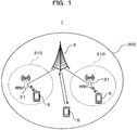
- FIG. 1 is a diagram illustrating an example of a wireless communication system according to an embodiment.
- the wireless communication system 1 illustrated in FIG. 1 may include, for example, one or more base stations 3 and one or more terminals 5.
- the base station 3 may be connected to a core network which is not illustrated.
- the base station 3 forms or provides a wireless area 300 available to communicate with the terminal 5.
- the "wireless area” may also be referred to as "cell”, “coverage area”, “communication area”, or “service area”.
- the base station 3 may be "eNB” compliant to the long term evolution (LTE) of 3rd generation partnership project (3GPP) or the LTE-Advanced (hereinafter collectively referred to as "LTE").
- LTE long term evolution
- 3GPP 3rd generation partnership project
- LTE-Advanced hereinafter collectively referred to as "LTE”
- the “eNB” is an abbreviation for "evolved Node B".
- the "cell” formed or provided by the base station 3 may be divided into “sector cells”.
- the term of "cell” may mean not only an individual geographical region where the base station 3 provides a wireless communication service but also all or a part of communication function used or managed by the base station 3 to communicate with the terminal 5 in the individual geographical region.
- the cell formed or provided by the eNB3 may be referred to as "macrocell” or “large cell”.
- the eNB3 that forms the macrocell 300 may be referred to as "macro base station”, “macro eNB”, or “MeNB”, for descriptive purposes.
- One or a plurality of small cells 310 may be disposed (overlaid) with respect to the macrocell 300.
- the small cell 310 is an example of a wireless area with a range (coverage), in which communication is available, smaller than that of the macrocell 300.
- the small cell 310 may be referred to differently depending on a size of coverage area.
- the small cell may also be referred to as "femto cell”, “pico cell”, “micro cell”, “nano cell”, “metro cell”, or "home cell”.
- the small cell 310 may also be formed or provided by a wireless device 31 disposed separately from a base station main unit.
- the wireless device 31 disposed separately from the base station main unit may be referred to as a remote radio equipment (RRE), or a remote radio head (RRH).
- RRE remote radio equipment
- RRH remote radio head
- the RRH 31 may be considered as an element of the base station 3, or may be considered as corresponding to another base station 3 different from the base station main unit that provides the macrocell 300. Further, the base station 3 may correspond to a relay device that relays communication for the terminal 5.
- the relay device may be a "Relay Node (RN)" compliant to LTE.
- the base stations 3 may be communicatively connected with each other by an X2 interface, for example.
- the X2 interface is an example of an interface between base stations, and may be any one of a wired interface and a wireless interface.
- the terminal 5 is available to perform wireless communications in one or both of the macrocell 300 and the small cell 310.
- the "terminal” may also be referred to as “wireless device”, “wireless apparatus”, or “terminal device”.
- the terminal 5 may be an immobile terminal or a mobile terminal (may also be referred to as a "mobile station").
- the terminal 5 may be a movable UE such as a mobile phone, a smart phone, or a tablet device.
- the "UE” is an abbreviation of "User Equipment”.
- the eNB3 may control a setting of wireless resources used for wireless communications with the UE5.
- the control of the setting of wireless resources may also be referred to as “allocation control of the wireless resources”.
- the allocation control of wireless resources (hereinafter, sometimes simply referred to as “resources”) may be referred to as a “scheduling".
- the scheduling may be performed individually for downlink (DL) communication and for uplink (UL) communication.
- the wireless resources may be distinguished in two dimensions of frequency domain and time domain, or may be distinguished in three dimensions of frequency domain, time domain, and power domain (or code domain).
- the eNB3 may schedule the wireless resources available for communications with the terminal 5 in units divided in two or three dimensions.
- the minimum unit of scheduling in LTE may be referred to as resource block (RB).
- the RB corresponds to one block obtained by dividing the resources available for the wireless communication between the eNB3 and the UE5 into units of slots in the time domain and a plurality of subcarriers neighboring in the frequency domain.
- the RB in LTE is represented by 2 slots * 12 subcarriers.
- One slot is 0.5 ms
- PRB Physical Resource Block
- PRB pair two PRBs within one subframe
- Time-division duplex (TDD) and the frequency-division duplex (FDD) may be applied to the wireless communication between the base station 3 and the terminal 5.
- DL communication and UL communication are performed at different timings by using one frequency (or one frequency band, the same applies hereinafter).
- the base station 3 schedules different timings for DL communication and UL communication in one frequency (or frequency band) for the terminal 5. Therefore, the base station 3 and the terminal 5 perform transmission and reception at different timings in one frequency.
- DL communication and UL communication are performed by using different frequencies (or frequency bands, the same applies hereinafter).
- the base station 3 may schedule different frequencies for DL communication and UL communication regardless of a timing of communication. Therefore, the base station 3 and the terminal 5 are available to perform reception at a frequency different from a transmission frequency while performing transmission.
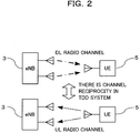
- the characteristics of DL and UL radio channels using the same frequency may be treated as being the same.
- the characteristics of the radio channel may be abbreviated as "channel characteristics", for descriptive purposes.
- UL channel characteristics estimated from a UL reference signal (RS) received from the UE5 may be treated as being equivalent to DL channel characteristics.
- the eNB3 is available to get the DL channel characteristics without receiving a report (feedback) of information indicative of the DL channel characteristics estimated by the UE5 from a DL RS, for example.
- the “reference signal” is an example of a known signal between the eNB3 and the UE5, and may also be referred to as a "pilot signal”.
- Information indicative of the estimated channel characteristics may also be referred to as a "channel estimated value”.
- the eNB3 is available to determine, for example, a precoding method and a transmission beamforming method used for DL data transmission in TDD by using a DL channel estimated value. For example, the eNB3 is available to control a weighting of a plurality of transmission data signal streams based on the DL channel estimated value.
- PMI is an abbreviation of "precoding matrix indicator”.
- the channel characteristics may be treated as being reciprocal between the UL and the DL as described above.
- the channel characteristics estimated by the eNB3 and the UE5 may differ depending on the difference in the response characteristics of the transceiver circuits of the eNB3 and the UE5.
- the eNB3 is provided with, for example, a first wireless (RF) transmission circuit Tx#1 and an RF reception circuit Rx#1 for the first antenna #1, and is provided with a second RF transmission circuit Tx#2 and an RF reception circuit Rx#2 for the second antenna #2.
- RF wireless
- the UE5 is provided with one RF reception circuit Rx#1 and one RF transmission circuit Tx#1 for one antenna #1.
- any one of the BB unit 301 provided in the eNB3 and the BB unit 501 provided in the UE5 is a unit that performs baseband (BB) signal processing on transmission and reception signals.
- BB baseband
- the RF transmission circuit and the RF reception circuit may be separate circuits, or may be integrated into a single circuit.
- a pair of the RF transmission circuit and the RF reception circuit may be collectively referred to as "RF transceiver circuit" or "RF circuit", for descriptive purposes.
- transfer functions of the first RF transmission circuit Tx#1 and the RF reception circuit Rx#1 in the eNB3 are respectively represented by T 1 and R 1
- transfer functions of the second RF transmission circuit Tx#2 and the RF reception circuit Rx#2 in the eNB3 are respectively represented by T 2 and R 2 .
- transfer functions of the RF reception circuit Rx#1 and the RF transmission circuit Tx#1 in the UE5 are represented by r 1 and t 1 , respectively.
- the above transfer functions in the eNB3 and the UE5 may be referred to as "RF circuit characteristics", for descriptive purposes.
- the channel matrix between the first antenna #1 of the eNB3 and the antenna #1 of the UE5 is represented by h 1,1
- the channel matrix between the second antenna #2 of the eNB3 and the antenna #1 of the UE5 is represented by h 1,2 .
- DL channel characteristics (F 1,1 ) estimated by the UE5 based on the DL RS transmitted by the eNB3 from the first antenna #1 can be expressed by the following mathematical formula 1.
- F 1 , 1 T 1 ⁇ h 1 , 1 ⁇ r 1
- UL channel characteristics (G 1,1 ) estimated by the eNB3 based on the UL RS transmitted by the UE5 from the antenna #1 can be expressed by the following mathematical formula 2.
- G 1 , 1 t 1 ⁇ h 1 , 1 ⁇ R 1
- DL throughput characteristics may be possibly degraded.
- the difference between the UL channel characteristics estimated by the eNB3 and the DL channel characteristics estimated by the UE5 is more influenced by the difference between the RF circuit characteristics for transmission and reception in the eNB3 than the difference between the RF circuit characteristics for transmission and reception in the UE5.
- the "MU-MIMO” is an abbreviation of "multi user-multiple-input and multiple-output”.
- the MIMO channel formed between them is expressed by an (M x N) channel matrix as set forth in the following mathematical formula 3.
- H h 0 , 0 ⁇ h 0 , N ⁇ 1 ⁇ ⁇ ⁇ h M ⁇ 1 , 0 ⁇ h M ⁇ 1 , N ⁇ 1
- a channel estimated result for the UL in the base station is expressed by a UL channel matrix G as set forth in the following mathematical formula 4.
- t m and rm represent a transfer function of a transceiver circuit for the antenna #m at the terminal
- T n and R n represent a transfer function of a transceiver circuit for the antenna #n at the base station.
- G t 0 ⁇ h 0 , 0 ⁇ R 0 ⁇ t 0 ⁇ h 0 , N ⁇ 1 ⁇ R N ⁇ 1 ⁇ ⁇ ⁇ t M ⁇ 1 ⁇ h M ⁇ 1 , 0 ⁇ R 0 ⁇ t M ⁇ 1 ⁇ h M ⁇ 1 , N ⁇ 1 ⁇ R N ⁇ 1
- a channel estimated result for the DL in each of the terminals is expressed by a DL channel matrix F as set forth in the following mathematical formula 5.
- B is a matrix representing a ratio of transceiver circuit responses for each antenna at the terminal
- A is a matrix representing a ratio of transceiver circuit responses for each antenna at the base station.
- the diag () represents a diagonal matrix.
- a ZF (Zero Forcing) transmission weight matrix W for the MU-MIMO transmission is expressed by the following mathematical formula 6 using the UL channel matrix G.
- the G H represents an adjoint matrix (or Hermitian transposed matrix) of the matrix G.
- W G H ⁇ G ⁇ G H ⁇ 1
- M transmission symbols (s 0 , ... , S M-1 ) for a plurality of terminals to perform a spatial multiplex transmission by N base station antennas M reception symbols (y 0 , ..., y M-1 ) received by the terminal are expressed by the following mathematical formula 7.
- the matrix A which is expressed by the following mathematical formula 8 and represents the ratio of the transceiver circuit response for each antenna at the base station has to be a constant multiple of the unit matrix.
- the equivalent channel is orthogonal.
- a state of the matrix B representing a ratio of the transceiver circuit response for each antenna at the terminal which is expressed by the following mathematical formula 9, does not influence on an orthogonality of the equivalent channel as compared with a base station side.
- B diag r 0 / t 0 , ⁇ r M ⁇ 1 / t M ⁇ 1
- the UL channel characteristics for each of the antennas #1 and #2 estimated in the eNB3 are corrected (may also be referred to as “calibrated”).
- the correction may be referred to as "RF circuit calibration", for descriptive purposes.
- the RF circuit calibrations can be classified into a “system calibration” and a “self calibration” depending on a signal used for calibration (may be referred to as “test signal” or “calibration signal”).
- the former "system calibration” may also be referred to as an "over-the-air calibration”.
- test signal it is preferable to transmit the test signal periodically or non-periodically to measure the RF circuit characteristics in order to perform correction following a temperature change or an aging of the RF transceiver circuit.
- the test signal is an example of a signal which is not directed for the terminal.
- FIG. 4 schematically illustrates an operation example of the system calibration. As indicated by dotted arrows in FIG. 4 , the eNB3 and the UE5 mutually transmit and receive test signals for calibration alternately, for example.
- the eNB3 may transmit a DL RS as an example of a test signal through the first RF transmission circuit Tx#1 and the antenna #1.
- the DL RS may be generated in the BB unit 301 of the eNB3, for example.
- the eNB3 may transmit an DL RS as an example of a test signal through the second RF transmission circuit Tx#2 and the antenna #2.
- the DL RS transmitted by each of the antennas #1 and #2 of the eNB3 is received by the RF reception circuit Rx#1 through the antenna #1 of the UE5 and input into the BB unit 501.
- the BB unit 501 may obtain DL channel estimated values from the received DL RSs. Each of the obtained DL channel estimated values may be transmitted (in other words, fed back) to the eNB3. The feedback to the eNB3 may be performed, for example, through the RF transmission circuit Tx#1 and the antenna #1 of the UE5.
- the UE5 may transmit a UL RS as an example of the test signal through the RF transmission circuit Tx#1 and the antenna #1.
- the UL RS may be transmitted at the same frequency as the UL RS at a timing different from the timing at which the DL RS is transmitted.
- the UL RS may be generated in the BB unit 501 of the UE5, for example.
- the UL RSs are received by the RF reception circuits Rx#1 and Rx#2 through the respective antennas #1 and #2 of the eNB3 and input into the BB unit 301.
- the BB unit 301 may obtain UL channel estimated values from the respective UL RSs received in the RF reception circuits Rx#1 and Rx#2. Then, the BB unit 301 may calculate a calibration coefficient by comparing the obtained UL channel estimated value with the DL channel estimated value fed back from the UE5.
- the eNB3 it is possible to make a relative relationship of the response characteristics between the RF transmission circuit and the RF reception circuit to converge into a constant phase difference ( ⁇ ) for any of the antennas #1 and #2.
- FIG. 5 schematically illustrates an operation example of self-calibration in the eNB3.
- the eNB3 alternately transmits and receives the test signal between the antennas #1 and #2, and compares the respective received test signals, for example, in the BB unit 301, whereby the calibration coefficient can be calculated.
- the processing of alternately transmitting and receiving test signals between the antennas #1 and #2 may be achieved by transmitting and receiving test signals with weak radio waves alternately between the antennas #1 and #2, for example, as illustrated by a two-dot chain line in FIG. 5 .
- the processing of alternately transmitting and receiving test signals between the antennas #1 and #2 may be achieved by alternately causing the test signal transmitted from one of the antennas #1 and #2 to branch with, for example, a coupler so as to input into the other of the antennas #1 and #2.
- the eNB3 it is possible to make a relative relationship of the response characteristics between the RF transmission circuit and the RF reception circuit to converge into a constant phase difference ( ⁇ ) for any of the antennas #1 and #2.
- a guard period may be provided in order to avoid an overlap (may also be referred to as a "collision” or an "interference") between a DL signal and a UL signal.
- the GP may be set in a subframe of the radio frame, which is referred to as a special subframe (SS) in LTE.
- SS special subframe
- the GP set in the SS may have a variable length.
- a GP having a time length depending on a propagation delay of a signal between the eNB3 and the UE5 or a time taken for switching between a transmission processing and a reception processing in the eNB3 or the UE5 may be set in the SS. Since the propagation delay of the signal between the eNB3 and the UE5 depends on a cell radius, the GP depending on the propagation delay may be considered as a GP depending on the cell radius.
- the number of CAL signals to be transmitted and received in the GP also increases.
- the number of antennas of the eNB3 increases, the number of time-division multiplex of the CAL signals in the GP increases.
- the CAL signals are bi-directionally transmitted for the (N-1) sets of antenna pairs.
- the GP length may be insufficient for the number of CAL signals to be transmitted and received.
- FIG. 7 schematically illsutrates an example in which the resources for the data signal are consumed by transmission and reception of the CAL signals.
- (1) and (2) respectively illustrate examples of signal transmission and reception timings for the antennas #1 and #2 of the eNB3, and (3) illustrates an example of signal transmission and reception timings of the UE5.
- the horizontal axis is the time axis, and OFDM symbols of DL signal, GPs, and OFDM symbols of UL signal are illustrated in order from the left.
- the "OFDM” is an abbreviation of "orthogonal frequency division multiplexing".
- the eNB3 may transmit DL data signals from one or both of the antennas #1 and #2 to the UE5. Meanwhile, in the OFDM symbols of the UL signal, the UE5 may transmit UL data signals.
- the number of OFDM symbols of the DL signal corresponds to a DL transmission period for the eNB3, and corresponds to a DL reception period for the UE5.
- the number of OFDM symbols of the UL signal corresponds to a UL transmission period for the UE5, and corresponds to a UL reception period for the eNB3.
- the eNB3 may transmit and receive the CAL signals between the antennas #1 and #2. For example, the eNB3 may transmit a first CAL signal #1 from the antenna #1 to the antenna #2, and then transmit a second CAL signal #2 from the antenna #2 to the antenna #1.
- a gap (GAP) #1 may be set between an OFDM symbol of a DL signal and a reception period of a CAL signal #1.
- the "GAP” means a period during which any signals are not transmitted and received.
- a GAP #2 may be set between a reception period of the CAL signal #1 and a transmission period of the CAL signal #2.
- the GAP #2 may be set in consideration of a time taken to switch between reception processing of the CAL signal #1 and transmission processing of the CAL signal #2.
- the GAP #3 may also be set between the transmission period of the CAL signal #2 and an OFDM symbol of the UL signal.
- a GAP #4 may be set between a transmission period of the CAL signal #1 and a reception period of the CAL signal #2.
- the GAP #4 may be set in consideration of a time taken to switch between transmission processing of the CAL signal #1 and reception processing of the CAL signal #2.
- the UE 5 may experience a large GAP #5 depending on lengths of the GAPs #1 to #4 between a DL reception period and a UL transmission period.
- the UL transmission timing would be started, at the fastest, in the middle of the transmission and reception processing between the antennas #1 and #2 of the second CAL signal #2.
- the UE5 When there is no transmission and reception of the CAL signals #1 and #2, the UE5 would originally be available to start a UL data transmission after the end of the DL reception period, for example, during a period in which the CAL signal #1 is transmitted from the antenna #1 to the antenna #2.
- the present embodiment achieves that a resource amount wasted by the CAL signals even when the number of antennas N that transmit and receive the CAL signals is large at the eNB3.
- the present embodiment provides a way to achieve the RF circuit calibration for a large-scale antenna system while minimizing the resource amount consumed by the CAL signals.
- FIG. 8 illustrates an example of the UL-DL configuration defined for the TDD frame format.
- the UL-DL configuration is defined in seven types indicated by configuration numbers "0" to "6". With the seven types of the UL-DL configuration, it is available to vary a ratio in the subframes for the DL and the UL to be set in the radio frame.
- a DL subframe is denoted by "D” and a UL subframe is denoted by "U”.
- One subframe is constituted by two slots (0.5 ms).
- One slot may be constituted by 6 or 7 symbols.
- the symbol may be an OFDM symbol, for example.
- a normal cyclic prefix (CP) is applied, 7 OFDM symbols are included in one slot.
- an extended CP having a longer time length than the normal CP is applied, 6 OFDM symbols are included in one slot.
- a special subframe represented by "S” may be set in order to facilitate switching from the DL subframe to the UL subframe.
- One SS may include 14 symbols, for example.
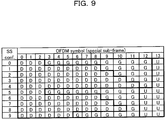
- FIG. 9 illustrates an example of an SS configuration. As illustrated in FIG. 9 , the SS configuration is defined in ten types indicated by configuration numbers "0" to "9".
- DwPTS downlink pilot time slot
- GP GP
- UpPTS uplink pilot time slot
- the "DwPTS” indicates a time slot for a DL communication in the SS
- the "UpPTS” indicates a time slot for a UL communication in the SS.
- the DwPTS may include 3 to 12 symbols
- the GP may include 2 to 10 symbols
- the UpPTS may include 1 or 2 symbols.
- the symbol of DwPTS may include a DL data signal
- the symbol of UpPTS may include a UL RS and a random access preamble.
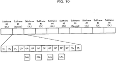
- the eNB3 sets a specific resource in the GP of the SS, and transmits and receives a CAL signal by using the resource.
- CAL signals can be multiplexed in the SS.
- the SS for which resource for a CAL signal (may be referred to as "CAL resource") is set may be selected from, for example, the ten types of SS configuration illustrated in FIG. 9 .
- CAL resource may be selected from, for example, the ten types of SS configuration illustrated in FIG. 9 .
- an SS configuration with a GP length sufficient to perform transmission and reception of a CAL signal may be selected.
- Such setting enables the RF circuit calibration using the CAL resources while avoiding collision between the UL signal and the DL signal in normal cellular communication in the macrocell.
- the eNB3 may transmit information related to a timing of applying a selected SS configuration to the macrocell (may be referred to as "timing information" for descriptive purposes) to the UE 5 to notify.
- timing information may be periodic or aperiodic.
- the UE5 that receives the timing information from the eNB3 can recognize which SS configuration is applied at the timing of which SS in the radio frame. Different SS configurations to be applied may have different GP lengths in the SS. Therefore, the UE5 can recognize the timing at which the SS of different GP length is applied based on the timing information.
- the UE5 may control communication with the eNB3 so as not to perform the UL and DL communication in the GP of the SS configuration recognized based on the timing information.
- the UE5 may wait for UL and DL communications for a time corresponding to the first GP length.
- the UE5 may wait for UL and DL communications for a time corresponding to the second GP length shorter than the first GP length.
- the GP with the first GP length is an example of the first GP in the first SS to which the first SS configuration is applied
- the GP with the second GP length is an example of the second GP in the second SS to which the second SS configuration is applied.
- a waiting (or standby) time of communications by the UE5 is changed depending on a change of the SS configurations applied by the eNB3.
- the eNB3 may set CAL resources to the GP of the first GP length in the first SS configuration. Thus, transmission and reception of the CAL signal is performed in the SS where a communication standby time of the UE5 becomes longer.
- a communication standby time of the UE5 is shorter than the timing of selective application of the first SS configuration. Therefore, it is possible to suppress a waste of time resources due to a fixed application of the first SS configuration for transmission and reception of the CAL signal.
- the eNB3 adaptively changes the SS configuration to be applied depending on a necessity of setting of CAL resources and notifies the UE5 of the information related to the timing of selective application, whereby the eNB3 can optimize the communication standby time of the UE5. Therefore, it is possible to minimize the consumption of wireless resources for RF circuit calibration.
- FIG. 11 illustrates a configuration example of the eNB3 according to an embodiment.
- the eNB3 may include a centralized base band unit (CBBU) 31, and N wireless devices (for example, RRH) 32-1 to 32-N (#1 to #N).
- CBBU centralized base band unit
- RRH wireless devices
- the CBBU 31 and RRH 32-i may be connected with each other by using an optical fiber.
- CPRI may be applied to the connection using optical fibers.
- the "CPRI” is an abbreviation of "common public radio interface”.
- the RRH32-i may include an RF transmission circuit (Tx) 321-i, an RF reception circuit (Rx) 322-i, and an antenna 323-i.
- the RF transmission circuit 321-i may up-convert the transmission baseband signal received from the CBBU 31 to an RF signal to output to the antenna 323-i.
- the transmission RF signal may be amplified to the target transmission power, for example, by a high power amplifier (HPA).
- HPA high power amplifier
- the RF reception circuit 322-i may down-convert the RF signal received by the antenna 323-i to a baseband signal to output to the CBBU 31.
- the reception RF signal may be appropriately amplified, for example, by a low noise amplifier (LNA).
- LNA low noise amplifier
- the target of the RF circuit calibration in the eNB3 is the (N-1) pairs of antenna pairs as schematically illustrated in FIG. 6 .
- FIG. 11 as a representative example, a pair of the antenna 321-1 of the RRH 32-1 and the antenna 321-N of the RRH 32-N is illustrated, and illustrations of the other antenna pairs are omitted.
- the CBBU 31 may include a DL signal transmitter 311-i, a UL signal receiver 312-i, a CAL signal transmitter 313-i, a CAL signal receiver 314-i, switches (SW) 315-i and 316-i, and a channel (CH) estimated value corrector 317-i. Each of these units may be provided with only N sets corresponding to the number N of the RRHs 32-i. Further, the CBBU 31 may include a GP controller 318, a calibration coefficient calculator 319, and the storage 320.
- the DL signal transmitter 311-i may perform the transmission processing on the DL signal to be transmitted to the UE5 through the RRH 32-i to output to the switch 315-i.
- the transmission processing of the DL signal may include encoding and modulation of the transmission signal and weighting control for precoding transmission and beamforming transmission.
- the UL signal receiver 312-i may perform the reception processing on the UL signal received by the RRH 32-i to be input from the switch 316-i.
- the reception processing of the UL signal may include demodulation and decoding of the UL signal. Further, the reception processing of the UL signal may include channel estimation processing using a UL RS.
- the CAL signal transmitter 313-i may generate a CAL signal to be transmitted from the RRH 32-i to another RRH 32-j so as to output to the switch 315-i.
- j is an integer that satisfies any one of 1 to N and j ⁇ i.
- the CAL signal transmitter 313-i is an example of a transmitter that transmits a CAL signal being an example of a predetermined signal in the GP of the first SS out of the first and second SSs.
- the CAL signal receiver 314-i may receive the CAL signal received by the RRH 32-i to be input from the switch 316-i so as to process.
- the reception processing of the CAL signal may include the processing of obtaining a channel estimated value between the RRH 32-i and another RRH 32-j being the source of the CAL signal based on the received CAL signal.
- the obtained channel estimated value may be given to the CAL coefficient calculator 319 for the calculation of the calibration coefficient.
- the switch 315-i may selectively output any one of the signal input from the DL signal transmitter 311-i and the CAL signal input from the CAL signal transmitter 313-i to the RF transmission circuit 321-i of the RRH 32-i.
- the switch 316-i may selectively output the signal input from the RF reception circuit 322-i of the RRH 32-i to any one of the UL signal receiver 312-i and the CAL signal receiver 314-i.
- the output switching between the switches 315-i and 316-i may be controlled by the GP controller 318.
- the channel estimated value corrector 317-i may correct a UL channel estimated value calculated by the UL signal receiver 312-i by the calibration coefficient calculated by the CAL coefficient calculator 319.
- the corrected UL channel estimated value may be considered as being equivalent to a DL channel estimated value, and may be given to the DL signal transmitter 311-i and may be used for a weighting control for precoding transmission and beamforming transmission.
- the GP controller 318 may selectively apply the SS configuration with the first GP length and the SS configuration with the second GP length in the TDD with the UE5. In other words, the GP controller 318 selectively applies the first SS with the first GP and the second SS with the second GP.
- the GP controller 318 may generate information related to the timing of selective application of one or both of the first and second SS configurations. For example, the GP controller 318 may generate one or both of the timing information for applying the SS configuration with the first GP length and the timing information for applying the SS configuration with the second GP length.
- the first GP length may be longer than the second GP length.
- the GP controller 318 may set CAL resources to the first GP with long GP length.
- the timing information may be referred to as GP information or GP control information, and may be information indicative of a time period in a radio frame.
- the time period may be distinguished in slot units or may be distinguished in subframe units.
- the timing information to apply the SS configuration with the first GP length may be information indicative of the timing of the SS corresponding to the first time period.
- the timing information for applying the SS configuration with the second GP length may be information indicating the timing of the SS corresponding to the second time period.
- the transmission timing or the reception timing of the DL signal transmitter 311-i, the UL signal receiver 312-i, the CAL signal transmitter 313-i, and the CAL signal receiver 314-i may be controlled.
- the DL signal transmitter 311-i, the UL signal receiver 312-i, the CAL signal transmitter 313-i, and the CAL signal receiver 314-i may be considered as elements of the communication circuitry.
- the DL signal transmitter 311-i may be considered as an example of a communication circuitry to notify the UE5 of information related to the timing of selective application of the first and second SSs.
- the timing information for notifying the UE5 may be one or both of the timing information of the first SS and the timing information of the second SS.
- the UE5 can identify the other timing information based on the periodicity in the time axis of the TDD frame.
- the CAL coefficient calculator 319 may calculate a calibration coefficient by comparing bidirectional channel estimated values estimated based on CAL signals transmitted and received between a pair of different RRH 32-i and RRH 32-j.
- FIG. 11 illustrates that bidirectional channel estimated values between RRH 32-1 and RRH 32-N can be obtained.
- bidirectional channel estimated values are obtained for each of the (N-1) sets of RRH pairs.
- the obtained calibration coefficient may be given to the channel estimated value corrector 317-i.
- the channel estimated value corrector 317-i and the CAL coefficient calculator 319 may be considered as an example of a calibrator for calibrating the channel characteristics between antennas forming pairs in the eNB3 with the CAL signal.
- the storage 320 may store the data of each configuration illustrated in FIGS. 8 and 9 .
- the GP controller 318 may determine the UL-DL configuration and the SS configuration to be applied based on the configuration data stored in the storage 320.
- the channel estimated value related to the calculation of the CAL coefficient by the CAL coefficient calculator 319 and the calculated calibration coefficient may be stored in the storage 320. Further, programs and data for achieving the operation of the eNB3 may be stored in the storage 320.
- Semiconductor memories such as a RAM (random access memory) and a ROM (read only memory), a hard disk drive (HDD), a solid-state drive (SSD), and the like may be applied to the storage 320.
- RAM random access memory
- ROM read only memory
- HDD hard disk drive
- SSD solid-state drive
- transmitters 311-i and 313-i, receivers 312-i and 314-i, the CH estimated value corrector 317-i, the GP controller 318, and all or part of the CAL coefficient calculator 319 may be achieved by using a hardware circuit having arithmetic processing capability.
- An example of a hardware circuit having arithmetic processing capability is a CPU (central processing unit), a DSP (digital signal processor), an MPU (micro processing unit), an IC (integrated circuit), an FPGA (field-programmable gate array), and the like.
- the hardware circuit having arithmetic processing capability may be referred to as "computer”.
- Various functions of the eNB3 may be embodied by the computer reading the program (may be referred to as “software” or “application”) and data stored in the storage 320 to operate.
- the program and data may be provided in a form recorded on a computer readable recording medium such as a flexible disk, a CD-ROM, a CD-R, a CD-RW, an MO, a DVD, a Blu-ray disk, a portable hard disk, a USB memory, or the like. Further, the program and data may be provided (for example, downloaded) from the server or the like to the eNB3 through a communication line.
- a computer readable recording medium such as a flexible disk, a CD-ROM, a CD-R, a CD-RW, an MO, a DVD, a Blu-ray disk, a portable hard disk, a USB memory, or the like.
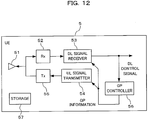
- the UE5 may include an antenna 51, an RF reception circuit (Rx) 52, a DL signal receiver 53, a UL signal transmitter 54, an RF transmission circuit (Tx) 55, a GP controller 56, and storage 57.
- Rx RF reception circuit
- Tx RF transmission circuit
- the antenna 51 receives the RF signal of the DL transmitted by the eNB3 and transmits the RF signal of the UL addressed to the eNB3.
- the RF reception circuit 52 may down-converts the RF signal of the DL received by the antenna 51 into a baseband signal to perform reception processing.
- the reception RF signal may be appropriately amplified by, for example, an LNA.
- the DL signal receiver 53 performs reception processing on the reception baseband signal of the DL input from the RF reception circuit 52.
- the reception processing of the DL may include demodulation and decoding of the DL signal and channel estimation of the DL.
- the channel estimation of the DL may be performed based on, for example, the DL RS or the pilot signal. Further, the demodulation and decoding result of the DL signal may include the control signal of the DL. The above-described GP control information may be included in the control signal of the DL. Therefore, the DL signal receiver 53 is an example of a receiver that receives information related to the timing of selective application of the first and second SSs selectively applied by the eNB3.
- the UL signal transmitter 54 may perform transmission processing of the UL signal to be transmitted to the eNB3.
- the UL signal may include the RS of the UL and pilot signals. Further, the transmission processing of the UL signal may include coding and modulation of the UL signal.
- the RF transmission circuit 55 may up-convert the UL signal input from the UL signal transmitter 54 to an RF signal to output to the antenna 51.
- the transmission RF signal may be amplified to the target transmission power, for example, by the HPA.
- the GP controller 56 may extract the GP control information from the control signal of the DL obtained by the reception processing of the DL signal receiver 53.
- the reception timing or transmission timing of the DL signal receiver 53 and the UL signal transmitter 54 may be controlled by the GP controller 56 based on the GP control information.
- the GP controller 56 may control the DL signal receiver 53 and the UL signal transmitter 54 so as to perform UL transmission or DL reception in the time slot other than the GP of the first SS and the GP of the second SS identified based on the GP control information.
- the DL signal receiver 53 and the UL signal transmitter 54 may be considered as an example of a communication circuitry that performs UL transmission or DL reception in the time slot other than the GP of the first SS and the GP of the second SS identified based on the GP control information.
- the storage 57 may store the data of each configuration illustrated in FIGS. 8 and 9 .
- the GP controller 56 can specify and identify the information related to the timing of selective application of the first and second SSs by referring to the configuration data stored in the storage 57, for example, based on the GP control information received from the eNB3.
- the GP control information received from the eNB may be stored in the storage 57. Further, programs and data for achieving the operation of the UE5 may be stored in the storage 57.
- Semiconductor memories such as a RAM and a ROM, an HDD, an SSD, and the like may be applied to the storage 57.
- the above-described DL signal receiver 53, UL signal transmitter 54, and all or a part of the GP controller 56 may be achieved by using a hardware circuit having arithmetic processing capability.
- An example of the hardware circuit having arithmetic processing capability is a CPU, a DSP, an MPU, an IC, an FPGA, or the like.
- the hardware circuit having arithmetic processing capability may be referred to as "computer”.
- Various functions of the UE5 may be embodied by the computer reading the program and data stored in the storage 57 to operate.
- the program and data may be provided in a form recorded on a computer readable recording medium such as a flexible disk, a CD-ROM, a CD-R, a CD-RW, an MO, a DVD, a Blu-ray disk, a portable hard disk, a USB memory, or the like. Further, the program and data may be provided (for example, downloaded) from the server or the like to the UE5 through a communication line.
- a computer readable recording medium such as a flexible disk, a CD-ROM, a CD-R, a CD-RW, an MO, a DVD, a Blu-ray disk, a portable hard disk, a USB memory, or the like.
- FIG. 13 is a sequence diagram illustrating an operation example of the wireless communication system 1
- FIG. 14 is a flowchart illustrating an operation example of the eNB3
- FIG. 15 is a flowchart illustrating an operation example of the UE5.
- the eNB3 transmits the GP control information to the UE5 to notify (process P11).
- the GP control information may be transmitted to the UE5 at the timing of transmitting the system information.
- the eNB3 monitors whether or not the transmission timing of the system information (for example, 80 ms cycle) has arrived (process P31).
- the eNB3 When the transmission timing of the system information arrives (YES in process P31), the eNB3 generates GP control information, for example, by the GP controller 318 to transmit to the UE5 (process P32).
- the GP control information may be included in a DL control signal peculiar to the UE5 connected to any one of the RRH 32-i.
- the eNB3 may shift the process to process P33 to be described below without performing the transmission processing of the GP control information.
- the GP control information may be included in a report signal to be reported to the wireless area provided by the RRH 32-i. Further, the GP control information may be transmitted from any of RRH 32-i. The GP control information may be transmitted from two or more of RRHs 32-i. FIG. 13 illustrates an example in which the GP control information is transmitted from the RRH 32-1 as one non-limiting example.
- the UE5 can recognize the timing of selective application T1 of the first SS corresponding to the first time period and the timing of selective application T2 of the second SS corresponding to the second time period by receiving the GP control information.
- the GP length in the first SS may be longer than the GP length in the second SS corresponding to the second time period.
- the occupation ratio of the GP may be larger than that of the (first) DwPTS or the (first) UpPTS.
- the occupation ratio of the GP may be smaller than that of the (second) DwPTS or the (second) UpPTS.
- the first SS may be a configuration of the SS configuration number "0" or "5" and the second SS may be a configuration of any one of the SS configuration numbers "1" to "4" and “6” to “9” illustrated in FIG. 9 .
- the UE5 connects to the eNB3 (process P51), and then monitors whether or not the reception timing of the system information from the eNB3 has arrived (process P52).
- the UE5 controls the reception processing of the DL signal receiver 53, for example, by the GP controller 56 to receive the control signal of the DL, whereby receives the GP control information included in the control signal of the DL (process P53).
- the UE5 may shift the process to process P54 to be described below without performing the reception processing of the GP control information.
- the eNB3 monitors whether or not the timing of selective application of the first time period has arrived (process P33).
- the eNB3 may generate and transmit the DL signal in the DwPTS in the SS corresponding to the first time period (process P34, process P12 in FIG. 13 ).
- the DL signal may be transmitted in three symbols of time slots of symbol numbers "0" to "2" indicated by "D".
- the DL signal may be a data signal.
- the transmission and reception of the CAL signal and the calculation of the calibration coefficient may be repeated as many times as the number of antenna pairs subject to the RF circuit calibration.
- the eNB3 may receive and demodulate the UL signal transmitted by the UE5 in the first UpPTS in the SS corresponding to the first time period (process P38, process P16 in FIG. 13 ).
- the UL signal may be transmitted by the UE5 in two symbols of time slots of symbol numbers "12" and "13" indicated by "U".
- the eNB3 may shift the process to process P31.
- the eNB3 may monitor whether or not the timing of selective application of the second time period has arrived (process P39).
- the eNB3 may generate and transmit the DL signal in the DwPTS in the SS corresponding to the second time period (process P40, process P17 in FIG. 13 ). Further, the eNB3 may receive and demodulate the UL signal transmitted by the UE5 in the UpPTS in the SS corresponding to the second time period (process P41, process P18 in FIG. 13 ).
- the eNB3 may shift the process to process P31.
- process P39 in FIG. 14 even when the timing of selective application of the second time period has not arrived, the eNB3 may shift the process to process P31.
- the UE5 monitors whether or not the timing of selective application of the first time period recognized by the GP control information has arrived (process P54).
- the UE5 may receive and demodulate the DL signal in the DwPTS of the SS corresponding to the first time period (process P55, process P12 in FIG. 13 ).
- the UE5 may generate and transmit the UL signal in the UpPTS of the SS corresponding to the first time period (process P56, process P16 in FIG. 13 ). Thereafter, the UE5 may shift the process to process P51.
- the UE5 may monitor whether or not the timing of selective application of the second time period has arrived (process P57).
- the UE5 may receive and demodulate the DL signal in the DwPTS in the SS corresponding to the second time period (process P58, process P17 in FIG. 13 ).
- the UE5 may generate and transmit the UL signal in the UpPTS of the SS corresponding to the second time period (process P59, process P18 in FIG. 13 ). Thereafter, the UE5 may shift the process to process P51. In process P57, even when the timing of selective application of the second time period has not arrived, the UE5 may shift the process to process P51.
- the UE5 may perform UL transmission or DL reception in the time slot other than the GP of the first SS and the GP of the second SS identified based on the timing information received from the eNB3.
- the wireless communication system 1 of TDD it is possible to achieve compatibility between the transmission of a predetermined signal such as the CAL signal by the base station 3 and the suppression of the decrease in the utilization efficiency of the wireless resources. For example, it is possible to transmit and receive CAL signals for large-scale antenna systems while minimizing the consumption of resources for ordinary cellular communications.
- the CAL signal for the RF circuit calibration is cited as an example of the predetermined signal transmitted by the base station 3 in the GP, the CAL signal may be a signal for other purposes.
- the signal for other purposes may be a signal that is not directed for the terminal.
- the predetermined signal may be a signal for measuring some physical variations between RRHs and making corrections in addition to calibration. For example, it is conceivable to measure and correct the variations of the carrier frequency caused by the local oscillator for each RRH.
- a pair of RRHs (for example, RRHs #1 and #2) are formed, and a predetermined signal is transmitted from RRH #1 to RRH #2 twice at certain nearby timings (for example, time difference ⁇ T).
- the RRH #2 can estimate the frequency difference between the RRH #1 and the RRH #2 by performing channel estimation by using the respective reception signals to check the phase change between the channel estimated values in ⁇ T.
- the compatibility between the transmission of the predetermined signal by the base station and the suppression of reduction in the utilization efficiency of the wireless resources can be achieved in the wireless communication system of time-division duplex communication.
Landscapes
- Engineering & Computer Science (AREA)
- Signal Processing (AREA)
- Computer Networks & Wireless Communication (AREA)
- Physics & Mathematics (AREA)
- Electromagnetism (AREA)
- Mobile Radio Communication Systems (AREA)
Abstract
Description
- The embodiments discussed herein are related to a wireless communication system, a base station, and a terminal.
- In a wireless communication system, a time-division duplex (TDD) under the same frequency may be applied to wireless communications between a base station and a terminal. In the TDD, a guard period (GP) may be set by the base station to enable a switching from downlink (DL) communication to uplink (UL) communication.
-
- Patent Document 1:
JP 2013-074486 A - Patent Document 2:
WO 2015/108007 A - Patent Document 3:
JP 2010-041269 A - Patent Document 4:
JP 2006-512807 W - Non-Patent Document 1: 3GPP R1-094641, "Performance study on Tx/Rx mismatch in LTE TDD Dual-layer beamforming", 3GPP TSG-RAN WG1 Meeting #59, November 9-13, 2009
- For example, it is assumed that the base station transmits a certain predetermined signal in the GP. An example of the predetermined signal transmitted in the GP may be some kind of test signal such as a calibration signal. The predetermined signal may be considered as "a signal which is not directed for the terminal".
- In this case, depending on a period during which the base station tries to transmit the predetermined signal, the GP may become insufficient. When a GP with a time length matching the period during which the base station tries to transmit the predetermined signal is applied, wireless resources available for terminals are reduced, and the utilization efficiency of the wireless resources may decrease.
- In one aspect, one of the objects of the techniques described herein is to achieve compatibility between a transmission of the predetermined signal by the base station and a suppression of reduction in the utilization efficiency of the wireless resources in the wireless communication system of TDD.
- In one aspect, a wireless communication system may include a terminal and a base station. The base station may selectively apply one of a first time period having a first guard period and a second time period having a second guard period to time-division duplex communication with a terminal. The base station may notify the terminal of information related to a timing of selectively applying one of the first time period and the second time period, and transmit a predetermined signal in the first guard period.
- Further, in one aspect, a base station may include a controller and a communication circuitry. The controller may selectively apply one of a first time period having a first guard period and a second time period having a second guard period to time-division duplex communication with a terminal. The communication circuitry may notify the terminal of information related to a timing of selectively applying one of the first time period and the second time period, and transmit a predetermined signal in the first guard period.
- Furthermore, in one aspect, a terminal configured to wirelessly communicate with a base station by time-division duplex communication may include a receiver and a communication circuitry. The receiver may receive information notified from the base station, the information being related to a timing of selectively applying one of a first time period having a first guard period and a second time period having a second guard period to the time-division duplex communication in the base station. The communication circuitry may perform transmission or reception in a time period other than the first and second guard periods. The time period may be identified based on the information.
- As one aspect, it is possible to achieve the compatibility between the transmission of the predetermined signal by the base station and the suppression of reduction in the utilization efficiency of the wireless resources in the wireless communication system of TDD.
-
-
FIG. 1 is a diagram illustrating an example of a wireless communication system according to an embodiment; -
FIG. 2 is a schematic diagram illustrating channel estimation in TDD; -
FIG. 3 is a diagram illustrating an influence of a wireless (RF) transceiver circuit on the channel estimated value; -
FIG. 4 is a schematic diagram illustrating a system calibration; -
FIG. 5 is a schematic diagram illustrating a self-calibration in a base station; -
FIG. 6 is a schematic diagram illustrating an example in which calibration signals are transmitted and received among a plurality of antennas provided in a base station; -
FIG. 7 is a schematic diagram illustrating an example in which resources are consumed for transmission and reception of a calibration signal; -
FIG. 8 is a diagram illustrating an example of an uplink-downlink (UL-DL) configuration; -
FIG. 9 is a diagram illustrating an example of a special subframe (SS) configuration; -
FIG. 10 is a diagram illustrating an example in which a wireless resource for a calibration signal is set in a guard period of SS; -
FIG. 11 is a block diagram illustrating a configuration example of a base station according to an embodiment; -
FIG. 12 is a block diagram illustrating a configuration example of a terminal according to an embodiment; -
FIG. 13 is a sequence diagram illustrating an operation example of the wireless communication system according to an embodiment; -
FIG. 14 is a flowchart illustrating an operation example of the base station according to an embodiment; and -
FIG. 15 is a flowchart illustrating an operation example of the terminal according to an embodiment. - Hereinafter, an exemplary embodiment(s) will be described with reference to the drawings. However, the embodiment(s) described below is merely an example and not intended to exclude an application of various modifications or techniques which are not explicitly described below. Further, various exemplary aspects described below may be appropriately combined and carried out. Elements or components assigned the same reference numeral in the drawings used for the following embodiment(s) will represent identical or similar elements or components unless otherwise specified.
-
FIG. 1 is a diagram illustrating an example of a wireless communication system according to an embodiment. Thewireless communication system 1 illustrated inFIG. 1 may include, for example, one ormore base stations 3 and one ormore terminals 5. Thebase station 3 may be connected to a core network which is not illustrated. - The
base station 3 forms or provides awireless area 300 available to communicate with theterminal 5. The "wireless area" may also be referred to as "cell", "coverage area", "communication area", or "service area". - The
base station 3 may be "eNB" compliant to the long term evolution (LTE) of 3rd generation partnership project (3GPP) or the LTE-Advanced (hereinafter collectively referred to as "LTE"). The "eNB" is an abbreviation for "evolved Node B". - The "cell" formed or provided by the
base station 3 may be divided into "sector cells". The term of "cell" may mean not only an individual geographical region where thebase station 3 provides a wireless communication service but also all or a part of communication function used or managed by thebase station 3 to communicate with theterminal 5 in the individual geographical region. - The cell formed or provided by the eNB3 may be referred to as "macrocell" or "large cell". The eNB3 that forms the
macrocell 300 may be referred to as "macro base station", "macro eNB", or "MeNB", for descriptive purposes. One or a plurality ofsmall cells 310 may be disposed (overlaid) with respect to themacrocell 300. - The
small cell 310 is an example of a wireless area with a range (coverage), in which communication is available, smaller than that of themacrocell 300. Thesmall cell 310 may be referred to differently depending on a size of coverage area. For example, the small cell may also be referred to as "femto cell", "pico cell", "micro cell", "nano cell", "metro cell", or "home cell". - The
small cell 310 may also be formed or provided by awireless device 31 disposed separately from a base station main unit. Thewireless device 31 disposed separately from the base station main unit may be referred to as a remote radio equipment (RRE), or a remote radio head (RRH). - The
RRH 31 may be considered as an element of thebase station 3, or may be considered as corresponding to anotherbase station 3 different from the base station main unit that provides themacrocell 300. Further, thebase station 3 may correspond to a relay device that relays communication for theterminal 5. The relay device may be a "Relay Node (RN)" compliant to LTE. - When two or
more base stations 3 are provided in thewireless communication system 1, thebase stations 3 may be communicatively connected with each other by an X2 interface, for example. The X2 interface is an example of an interface between base stations, and may be any one of a wired interface and a wireless interface. - The
terminal 5 is available to perform wireless communications in one or both of themacrocell 300 and thesmall cell 310. The "terminal" may also be referred to as "wireless device", "wireless apparatus", or "terminal device". - The
terminal 5 may be an immobile terminal or a mobile terminal (may also be referred to as a "mobile station"). As a non-limiting example, theterminal 5 may be a movable UE such as a mobile phone, a smart phone, or a tablet device. The "UE" is an abbreviation of "User Equipment". - The eNB3 may control a setting of wireless resources used for wireless communications with the UE5. The control of the setting of wireless resources may also be referred to as "allocation control of the wireless resources". The allocation control of wireless resources (hereinafter, sometimes simply referred to as "resources") may be referred to as a "scheduling".
- The scheduling may be performed individually for downlink (DL) communication and for uplink (UL) communication.
- The wireless resources may be distinguished in two dimensions of frequency domain and time domain, or may be distinguished in three dimensions of frequency domain, time domain, and power domain (or code domain).
- The eNB3 may schedule the wireless resources available for communications with the
terminal 5 in units divided in two or three dimensions. For example, the minimum unit of scheduling in LTE may be referred to as resource block (RB). - The RB corresponds to one block obtained by dividing the resources available for the wireless communication between the eNB3 and the UE5 into units of slots in the time domain and a plurality of subcarriers neighboring in the frequency domain.
- For example, the RB in LTE is represented by 2 slots * 12 subcarriers. One slot is 0.5 ms, and one subframe includes 2 slots (2 * 0.5 ms = 1 ms). One radio frame includes 10 subframes (10 * 1 ms = 10 ms). In LTE, a unit of 1 slot * 12 subcarriers may be referred to as a PRB (Physical Resource Block), and two PRBs within one subframe may be referred to as a "PRB pair".
- Any one of the time-division duplex (TDD) and the frequency-division duplex (FDD) may be applied to the wireless communication between the
base station 3 and theterminal 5. - In TDD, DL communication and UL communication are performed at different timings by using one frequency (or one frequency band, the same applies hereinafter).
- For example, the
base station 3 schedules different timings for DL communication and UL communication in one frequency (or frequency band) for theterminal 5. Therefore, thebase station 3 and theterminal 5 perform transmission and reception at different timings in one frequency. - Meanwhile, in FDD, DL communication and UL communication are performed by using different frequencies (or frequency bands, the same applies hereinafter). For example, the
base station 3 may schedule different frequencies for DL communication and UL communication regardless of a timing of communication. Therefore, thebase station 3 and theterminal 5 are available to perform reception at a frequency different from a transmission frequency while performing transmission. - In TDD, as schematically illustrated in
FIG. 2 , since there is a reciprocity between the DL and UL radio channels between thebase station 3 and theterminal 5, the characteristics of DL and UL radio channels using the same frequency may be treated as being the same. The characteristics of the radio channel may be abbreviated as "channel characteristics", for descriptive purposes. - For example, in the eNB3, UL channel characteristics estimated from a UL reference signal (RS) received from the UE5 may be treated as being equivalent to DL channel characteristics. In other words, the eNB3 is available to get the DL channel characteristics without receiving a report (feedback) of information indicative of the DL channel characteristics estimated by the UE5 from a DL RS, for example.
- The "reference signal" is an example of a known signal between the eNB3 and the UE5, and may also be referred to as a "pilot signal". Information indicative of the estimated channel characteristics may also be referred to as a "channel estimated value".
- The eNB3 is available to determine, for example, a precoding method and a transmission beamforming method used for DL data transmission in TDD by using a DL channel estimated value. For example, the eNB3 is available to control a weighting of a plurality of transmission data signal streams based on the DL channel estimated value.
- Further, for example, since a report of a PMI from the UE5 to the eNB3 can be eliminated, it is possible to reduce an overhead of an UL control signal involved in the report. The "PMI" is an abbreviation of "precoding matrix indicator".
- In TDD, as for the radio channel in the air, the channel characteristics may be treated as being reciprocal between the UL and the DL as described above. However, in practice, the channel characteristics estimated by the eNB3 and the UE5 may differ depending on the difference in the response characteristics of the transceiver circuits of the eNB3 and the UE5.
- For example, as schematically illustrated in
FIG. 3 , it is assumed a model in which two antennas (ANT) #1 and #2 are provided for the eNB3 and one antenna (ANT) #1 is provided for the UE5. - The eNB3 is provided with, for example, a first wireless (RF) transmission
circuit Tx# 1 and an RF receptioncircuit Rx# 1 for thefirst antenna # 1, and is provided with a second RF transmissioncircuit Tx# 2 and an RF receptioncircuit Rx# 2 for thesecond antenna # 2. - Meanwhile, the UE5 is provided with one RF reception
circuit Rx# 1 and one RF transmissioncircuit Tx# 1 for oneantenna # 1. - In
FIG. 3 , any one of theBB unit 301 provided in the eNB3 and theBB unit 501 provided in the UE5 is a unit that performs baseband (BB) signal processing on transmission and reception signals. - In each of the eNB3 and the UE5, the RF transmission circuit and the RF reception circuit may be separate circuits, or may be integrated into a single circuit. In the following description, regardless of whether separate or integrated, a pair of the RF transmission circuit and the RF reception circuit may be collectively referred to as "RF transceiver circuit" or "RF circuit", for descriptive purposes.
- Here, transfer functions of the first RF transmission
circuit Tx# 1 and the RF receptioncircuit Rx# 1 in the eNB3 are respectively represented by T1 and R1, and transfer functions of the second RF transmissioncircuit Tx# 2 and the RF receptioncircuit Rx# 2 in the eNB3 are respectively represented by T2 and R2. - Further, transfer functions of the RF reception
circuit Rx# 1 and the RF transmissioncircuit Tx# 1 in the UE5 are represented by r1 and t1, respectively. The above transfer functions in the eNB3 and the UE5 may be referred to as "RF circuit characteristics", for descriptive purposes. - Furthermore, the channel matrix between the
first antenna # 1 of the eNB3 and theantenna # 1 of the UE5 is represented by h1,1, and the channel matrix between thesecond antenna # 2 of the eNB3 and theantenna # 1 of the UE5 is represented by h1,2. - In this case, DL channel characteristics (F1,1) estimated by the UE5 based on the DL RS transmitted by the eNB3 from the
first antenna # 1 can be expressed by the followingmathematical formula 1.
- Meanwhile, UL channel characteristics (G1,1) estimated by the eNB3 based on the UL RS transmitted by the UE5 from the
antenna # 1 can be expressed by the followingmathematical formula 2.
- Therefore, when T1 ≠ t1 or r1 ≠ R1 is satisfied, since G1,1 ≠ F1,1 is satisfied, by treating the UL channel characteristics G1,1 estimated by the eNB3 as the same as the DL channel characteristics F1,1 estimated by the UE5, the DL communication characteristics may be possibly degraded.
- For example, since the precoding transmission or the transmission beamforming for the DL based on the UL channel characteristics estimated by the eNB3 becomes non-optimal, DL throughput characteristics may be possibly degraded. The same applies to the DL transmission through the
second antenna # 2 of the eNB3. - There is a tendency that the difference between the UL channel characteristics estimated by the eNB3 and the DL channel characteristics estimated by the UE5 is more influenced by the difference between the RF circuit characteristics for transmission and reception in the eNB3 than the difference between the RF circuit characteristics for transmission and reception in the UE5.
- For example, the following cases will be discussed.
- When the MU-MIMO transmission between one base station and a plurality of terminals is performed, an influence caused by the transceiver circuit characteristics in the base station and the terminal will be considered. The "MU-MIMO" is an abbreviation of "multi user-multiple-input and multiple-output".
- When the number of antennas of the base station is represented by N and the total number of antennas of the plurality of terminals is represented by M, the MIMO channel formed between them is expressed by an (M x N) channel matrix as set forth in the following
mathematical formula 3.
- A channel estimated result for the UL in the base station is expressed by a UL channel matrix G as set forth in the following
mathematical formula 4. Here, tm and rm represent a transfer function of a transceiver circuit for the antenna #m at the terminal, and Tn and Rn represent a transfer function of a transceiver circuit for the antenna #n at the base station.
- Meanwhile, a channel estimated result for the DL in each of the terminals is expressed by a DL channel matrix F as set forth in the following
mathematical formula 5. Here, B is a matrix representing a ratio of transceiver circuit responses for each antenna at the terminal, and A is a matrix representing a ratio of transceiver circuit responses for each antenna at the base station. The diag () represents a diagonal matrix.
- A ZF (Zero Forcing) transmission weight matrix W for the MU-MIMO transmission is expressed by the following
mathematical formula 6 using the UL channel matrix G. The GH represents an adjoint matrix (or Hermitian transposed matrix) of the matrix G.
- When ZF transmission weights are applied to M transmission symbols (s0, ... , SM-1) for a plurality of terminals to perform a spatial multiplex transmission by N base station antennas, M reception symbols (y0, ..., yM-1) received by the terminal are expressed by the following
mathematical formula 7.
- When an equivalent channel (F·W) between the base station and the terminal is in a state represented by a diagonal matrix, the channel is orthogonal, and transmission symbols for a plurality of terminals are received without interfering with each other. To that end, the matrix A which is expressed by the following
mathematical formula 8 and represents the ratio of the transceiver circuit response for each antenna at the base station has to be a constant multiple of the unit matrix.
- When the above conditions can be satisfied, the equivalent channel is orthogonal. Meanwhile, it can be considered that a state of the matrix B representing a ratio of the transceiver circuit response for each antenna at the terminal, which is expressed by the following
mathematical formula 9, does not influence on an orthogonality of the equivalent channel as compared with a base station side.
- In order to avoid or suppress a deterioration of the DL communication characteristics as described above, it is preferred that the UL channel characteristics for each of the
antennas # 1 and #2 estimated in the eNB3 are corrected (may also be referred to as "calibrated"). The correction may be referred to as "RF circuit calibration", for descriptive purposes. - The RF circuit calibrations can be classified into a "system calibration" and a "self calibration" depending on a signal used for calibration (may be referred to as "test signal" or "calibration signal"). The former "system calibration" may also be referred to as an "over-the-air calibration".
- In any of the calibrations, it is preferable to transmit the test signal periodically or non-periodically to measure the RF circuit characteristics in order to perform correction following a temperature change or an aging of the RF transceiver circuit. The test signal is an example of a signal which is not directed for the terminal.
-
FIG. 4 schematically illustrates an operation example of the system calibration. As indicated by dotted arrows inFIG. 4 , the eNB3 and the UE5 mutually transmit and receive test signals for calibration alternately, for example. - For example, the eNB3 may transmit a DL RS as an example of a test signal through the first RF transmission
circuit Tx# 1 and theantenna # 1. The DL RS may be generated in theBB unit 301 of the eNB3, for example. - Similarly, the eNB3 may transmit an DL RS as an example of a test signal through the second RF transmission
circuit Tx# 2 and theantenna # 2. - The DL RS transmitted by each of the
antennas # 1 and #2 of the eNB3 is received by the RF receptioncircuit Rx# 1 through theantenna # 1 of the UE5 and input into theBB unit 501. - The
BB unit 501 may obtain DL channel estimated values from the received DL RSs. Each of the obtained DL channel estimated values may be transmitted (in other words, fed back) to the eNB3. The feedback to the eNB3 may be performed, for example, through the RF transmissioncircuit Tx# 1 and theantenna # 1 of the UE5. - Further, the UE5 may transmit a UL RS as an example of the test signal through the RF transmission
circuit Tx# 1 and theantenna # 1. The UL RS may be transmitted at the same frequency as the UL RS at a timing different from the timing at which the DL RS is transmitted. The UL RS may be generated in theBB unit 501 of the UE5, for example. - The UL RSs are received by the RF reception
circuits Rx# 1 andRx# 2 through therespective antennas # 1 and #2 of the eNB3 and input into theBB unit 301. - The
BB unit 301 may obtain UL channel estimated values from the respective UL RSs received in the RF receptioncircuits Rx# 1 andRx# 2. Then, theBB unit 301 may calculate a calibration coefficient by comparing the obtained UL channel estimated value with the DL channel estimated value fed back from the UE5. - By correcting the channel characteristics using the calculated calibration coefficient, it is possible to fix the responses of the RF transceiver circuits for all
antennas # 1 and #2 to the same or a constant relationship. - For example, in the eNB3, it is possible to make a relative relationship of the response characteristics between the RF transmission circuit and the RF reception circuit to converge into a constant phase difference (ϕ) for any of the
antennas # 1 and #2. -
FIG. 5 schematically illustrates an operation example of self-calibration in the eNB3. - In the self-calibration, the eNB3 alternately transmits and receives the test signal between the
antennas # 1 and #2, and compares the respective received test signals, for example, in theBB unit 301, whereby the calibration coefficient can be calculated. - The processing of alternately transmitting and receiving test signals between the
antennas # 1 and #2 may be achieved by transmitting and receiving test signals with weak radio waves alternately between theantennas # 1 and #2, for example, as illustrated by a two-dot chain line inFIG. 5 . - Alternatively, the processing of alternately transmitting and receiving test signals between the
antennas # 1 and #2 may be achieved by alternately causing the test signal transmitted from one of theantennas # 1 and #2 to branch with, for example, a coupler so as to input into the other of theantennas # 1 and #2. - By correcting the channel characteristics by using the calculated calibration coefficient, it is possible to fix the response of the RF transceiver circuit for all
antennas # 1 and #2 to the same or a constant relationship. - For example, in the eNB3, it is possible to make a relative relationship of the response characteristics between the RF transmission circuit and the RF reception circuit to converge into a constant phase difference (ϕ) for any of the
antennas # 1 and #2. - In a radio frame of TDD, a guard period (GP) may be provided in order to avoid an overlap (may also be referred to as a "collision" or an "interference") between a DL signal and a UL signal. The GP may be set in a subframe of the radio frame, which is referred to as a special subframe (SS) in LTE.
- The GP set in the SS may have a variable length. For example, A GP having a time length depending on a propagation delay of a signal between the eNB3 and the UE5 or a time taken for switching between a transmission processing and a reception processing in the eNB3 or the UE5 may be set in the SS. Since the propagation delay of the signal between the eNB3 and the UE5 depends on a cell radius, the GP depending on the propagation delay may be considered as a GP depending on the cell radius.
- Here, when transmission and reception of calibration (CAL) signals for the RF circuit calibration are performed in the GP, resources are not consumed for the UL signal and the DL signal used for the RF circuit calibration, and therefore, it can be considered to be advantageous from the viewpoint of utilization efficiency of resources.
- However, for example, as the number of antennas increases due to an increase in size of the antenna system used for precoding transmission and beamforming transmission increases, the number of CAL signals to be transmitted and received in the GP also increases. In other words, as the number of antennas of the eNB3 increases, the number of time-division multiplex of the CAL signals in the GP increases.
- For example, as schematically illustrated in
FIG. 6 , when the number of antennas of the eNB3 is N (N is an integer of 2 or more), the CAL signals are bi-directionally transmitted for the (N-1) sets of antenna pairs. - Therefore, for example, as the number of antennas N increases as in a large-scale antenna system, there is a possibility that transmissions and receptions of the CAL signals sufficient in number for the RF circuit calibration are not finished in the GP. In other words, the GP length may be insufficient for the number of CAL signals to be transmitted and received.
- When the GP is lengthened depending on the number of CAL signals to be transmitted and received in order to avoid the insufficient GP length, resource amount available for transmission of a data signal decreases. Since the RF circuit calibration does not need to be performed frequently, when a resource for the data signals is consumed by temporal and intermittent transmission or reception of a CAL signal, throughput characteristics between the eNB3 and the UE5 may decrease.
-
FIG. 7 schematically illsutrates an example in which the resources for the data signal are consumed by transmission and reception of the CAL signals. InFIG. 7 , (1) and (2) respectively illustrate examples of signal transmission and reception timings for theantennas # 1 and #2 of the eNB3, and (3) illustrates an example of signal transmission and reception timings of the UE5. - In
FIG. 7 , the horizontal axis is the time axis, and OFDM symbols of DL signal, GPs, and OFDM symbols of UL signal are illustrated in order from the left. The "OFDM" is an abbreviation of "orthogonal frequency division multiplexing". - In the OFDM symbols of the DL signal, the eNB3 may transmit DL data signals from one or both of the
antennas # 1 and #2 to the UE5. Meanwhile, in the OFDM symbols of the UL signal, the UE5 may transmit UL data signals. - Therefore, the number of OFDM symbols of the DL signal corresponds to a DL transmission period for the eNB3, and corresponds to a DL reception period for the UE5. Meanwhile, the number of OFDM symbols of the UL signal corresponds to a UL transmission period for the UE5, and corresponds to a UL reception period for the eNB3.
- In the GP, the eNB3 may transmit and receive the CAL signals between the
antennas # 1 and #2. For example, the eNB3 may transmit a firstCAL signal # 1 from theantenna # 1 to theantenna # 2, and then transmit a secondCAL signal # 2 from theantenna # 2 to theantenna # 1. - Here, as illustrated in (2) of
FIG. 7 , in order to avoid collision at theantenna # 2 between a DL data signal transmission and a reception of the CAL signal from theantenna # 1, a gap (GAP) #1 may be set between an OFDM symbol of a DL signal and a reception period of aCAL signal # 1. The "GAP" means a period during which any signals are not transmitted and received. - Further, in order to avoid collision at the
antenna # 2 between a reception of theCAL signal # 1 and a transmission of theCAL signal # 2, aGAP # 2 may be set between a reception period of theCAL signal # 1 and a transmission period of theCAL signal # 2. TheGAP # 2 may be set in consideration of a time taken to switch between reception processing of theCAL signal # 1 and transmission processing of theCAL signal # 2. - Furthermore, in order to avoid collision at the
antenna # 2 between the transmission of theCAL signal # 2 and a reception of UL data signal, theGAP # 3 may also be set between the transmission period of theCAL signal # 2 and an OFDM symbol of the UL signal. - Meanwhile, focusing on the
antenna # 1, as illustrated in (1) ofFIG. 7 , in order to avoid collision at theantenna # 1 between a transmission of theCAL signal # 1 and a reception of theCAL signal # 2, aGAP # 4 may be set between a transmission period of theCAL signal # 1 and a reception period of theCAL signal # 2. TheGAP # 4 may be set in consideration of a time taken to switch between transmission processing of theCAL signal # 1 and reception processing of theCAL signal # 2. - In such a way, when the
GAPs # 1 to #4 are set to transmit and receive CAL signals betweenantennas # 1 and #2, as illustrated in (3) ofFIG. 7 , theUE 5 may experience alarge GAP # 5 depending on lengths of theGAPs # 1 to #4 between a DL reception period and a UL transmission period. - For example, after the end of the DL reception period, even when the UE5 can advance a UL transmission timing by a time depending on a UL propagation delay, the UL transmission timing would be started, at the fastest, in the middle of the transmission and reception processing between the
antennas # 1 and #2 of the secondCAL signal # 2. - When there is no transmission and reception of the CAL signals #1 and #2, the UE5 would originally be available to start a UL data transmission after the end of the DL reception period, for example, during a period in which the
CAL signal # 1 is transmitted from theantenna # 1 to theantenna # 2. - Thus, when the CAL signal is transmitted and received between the
antennas # 1 and #2 of the eNB3 during the GP, time resources which would be originally available for a UL transmission by the UE5 may be wasted depending on the GAP length set for transmission and reception of the CAL signal. - In view of the above, the present embodiment achieves that a resource amount wasted by the CAL signals even when the number of antennas N that transmit and receive the CAL signals is large at the eNB3.
- In other words, the present embodiment provides a way to achieve the RF circuit calibration for a large-scale antenna system while minimizing the resource amount consumed by the CAL signals.
- For example, a TDD frame format of LTE is focused.
FIG. 8 illustrates an example of the UL-DL configuration defined for the TDD frame format. - As illustrated in
FIG. 8 , the UL-DL configuration is defined in seven types indicated by configuration numbers "0" to "6". With the seven types of the UL-DL configuration, it is available to vary a ratio in the subframes for the DL and the UL to be set in the radio frame. InFIG. 8 , a DL subframe is denoted by "D" and a UL subframe is denoted by "U". - In the TDD frame format of LTE, one radio frame is constituted by ten subframes with
subframe numbers 0 to 9 (1 ms), and has a time length of 10 * 1 ms = 10 ms. One subframe is constituted by two slots (0.5 ms). - One slot may be constituted by 6 or 7 symbols. The symbol may be an OFDM symbol, for example. When a normal cyclic prefix (CP) is applied, 7 OFDM symbols are included in one slot. Meanwhile, when an extended CP having a longer time length than the normal CP is applied, 6 OFDM symbols are included in one slot.
- In the TDD frame, as illustrated in
FIG. 8 , a special subframe (SS) represented by "S" may be set in order to facilitate switching from the DL subframe to the UL subframe. One SS may include 14 symbols, for example. -
FIG. 9 illustrates an example of an SS configuration. As illustrated inFIG. 9 , the SS configuration is defined in ten types indicated by configuration numbers "0" to "9". - In the SS, three fields of a downlink pilot time slot (DwPTS), a GP, and an uplink pilot time slot (UpPTS) are defined in units of symbols, for example. In
FIG. 9 , "D" denotes "DwPTS", "G" denotes "GP", and "U" denotes "UpPTS". - The "DwPTS" indicates a time slot for a DL communication in the SS, and the "UpPTS" indicates a time slot for a UL communication in the SS. Depending on the types of the SS configuration, the DwPTS may include 3 to 12 symbols, the GP may include 2 to 10 symbols, and the UpPTS may include 1 or 2 symbols.
- The symbol of DwPTS may include a DL data signal, and the symbol of UpPTS may include a UL RS and a random access preamble.
- With 10 types of the SS configurations, it is available to vary the GP length in the SS in symbol units. As described above, with applying an appropriate SS configuration to the cell according to a propagation delay depending on the cell radius, it is available to set a GP having an appropriate time length depending on the propagation delay, for example.
- The eNB3 sets a specific resource in the GP of the SS, and transmits and receives a CAL signal by using the resource. Thus, CAL signals can be multiplexed in the SS.
- The SS for which resource for a CAL signal (may be referred to as "CAL resource") is set may be selected from, for example, the ten types of SS configuration illustrated in
FIG. 9 . For example, an SS configuration with a GP length sufficient to perform transmission and reception of a CAL signal may be selected. - As a non-limiting example, the eNB3 may apply the SS configuration = "5" to the macrocell in
FIG. 9 and may set all or a part of the 9 symbols of the GP with symbol numbers = 3 to 11 as the CAL resources (for example, seeFIG. 10 ). - Such setting enables the RF circuit calibration using the CAL resources while avoiding collision between the UL signal and the DL signal in normal cellular communication in the macrocell.
- The eNB3 may transmit information related to a timing of applying a selected SS configuration to the macrocell (may be referred to as "timing information" for descriptive purposes) to the
UE 5 to notify. In the eNB3, the timing of applying the SS configuration to the macrocell may be periodic or aperiodic. - The UE5 that receives the timing information from the eNB3 can recognize which SS configuration is applied at the timing of which SS in the radio frame. Different SS configurations to be applied may have different GP lengths in the SS. Therefore, the UE5 can recognize the timing at which the SS of different GP length is applied based on the timing information.
- The UE5 may control communication with the eNB3 so as not to perform the UL and DL communication in the GP of the SS configuration recognized based on the timing information.
- For example, at the timing of selective application of the first SS configuration having the first GP length, the UE5 may wait for UL and DL communications for a time corresponding to the first GP length.
- Further, at the timing of selective application of the second SS configuration having the second GP length shorter than the first GP length, the UE5 may wait for UL and DL communications for a time corresponding to the second GP length shorter than the first GP length.
- The GP with the first GP length is an example of the first GP in the first SS to which the first SS configuration is applied, and the GP with the second GP length is an example of the second GP in the second SS to which the second SS configuration is applied.
- Thus, a waiting (or standby) time of communications by the UE5 is changed depending on a change of the SS configurations applied by the eNB3.
- The eNB3 may set CAL resources to the GP of the first GP length in the first SS configuration. Thus, transmission and reception of the CAL signal is performed in the SS where a communication standby time of the UE5 becomes longer.
- At a timing of selective application of the second SS configuration, a communication standby time of the UE5 is shorter than the timing of selective application of the first SS configuration. Therefore, it is possible to suppress a waste of time resources due to a fixed application of the first SS configuration for transmission and reception of the CAL signal.
- In other words, the eNB3 adaptively changes the SS configuration to be applied depending on a necessity of setting of CAL resources and notifies the UE5 of the information related to the timing of selective application, whereby the eNB3 can optimize the communication standby time of the UE5. Therefore, it is possible to minimize the consumption of wireless resources for RF circuit calibration.
-
FIG. 11 illustrates a configuration example of the eNB3 according to an embodiment. As illustrated inFIG. 11 , the eNB3 may include a centralized base band unit (CBBU) 31, and N wireless devices (for example, RRH) 32-1 to 32-N (#1 to #N). - The
CBBU 31 and RRH 32-i (i is any one of 1 to N) may be connected with each other by using an optical fiber. For example, CPRI may be applied to the connection using optical fibers. The "CPRI" is an abbreviation of "common public radio interface". - The RRH32-i may include an RF transmission circuit (Tx) 321-i, an RF reception circuit (Rx) 322-i, and an antenna 323-i.
- The RF transmission circuit 321-i may up-convert the transmission baseband signal received from the
CBBU 31 to an RF signal to output to the antenna 323-i. The transmission RF signal may be amplified to the target transmission power, for example, by a high power amplifier (HPA). - The RF reception circuit 322-i may down-convert the RF signal received by the antenna 323-i to a baseband signal to output to the
CBBU 31. The reception RF signal may be appropriately amplified, for example, by a low noise amplifier (LNA). - Since one antenna 323-i is provided for each of the N RRHs 32-1 to 32-N, the number of antennas is also N. Therefore, the target of the RF circuit calibration in the eNB3 is the (N-1) pairs of antenna pairs as schematically illustrated in
FIG. 6 . - In
FIG. 11 , as a representative example, a pair of the antenna 321-1 of the RRH 32-1 and the antenna 321-N of the RRH 32-N is illustrated, and illustrations of the other antenna pairs are omitted. - The
CBBU 31 may include a DL signal transmitter 311-i, a UL signal receiver 312-i, a CAL signal transmitter 313-i, a CAL signal receiver 314-i, switches (SW) 315-i and 316-i, and a channel (CH) estimated value corrector 317-i. Each of these units may be provided with only N sets corresponding to the number N of the RRHs 32-i. Further, theCBBU 31 may include aGP controller 318, acalibration coefficient calculator 319, and thestorage 320. - The DL signal transmitter 311-i may perform the transmission processing on the DL signal to be transmitted to the UE5 through the RRH 32-i to output to the switch 315-i. The transmission processing of the DL signal may include encoding and modulation of the transmission signal and weighting control for precoding transmission and beamforming transmission.
- The UL signal receiver 312-i may perform the reception processing on the UL signal received by the RRH 32-i to be input from the switch 316-i. The reception processing of the UL signal may include demodulation and decoding of the UL signal. Further, the reception processing of the UL signal may include channel estimation processing using a UL RS.
- The CAL signal transmitter 313-i may generate a CAL signal to be transmitted from the RRH 32-i to another RRH 32-j so as to output to the switch 315-i. Here, j is an integer that satisfies any one of 1 to N and j ≠ i. The CAL signal transmitter 313-i is an example of a transmitter that transmits a CAL signal being an example of a predetermined signal in the GP of the first SS out of the first and second SSs.
- The CAL signal receiver 314-i may receive the CAL signal received by the RRH 32-i to be input from the switch 316-i so as to process. The reception processing of the CAL signal may include the processing of obtaining a channel estimated value between the RRH 32-i and another RRH 32-j being the source of the CAL signal based on the received CAL signal. The obtained channel estimated value may be given to the
CAL coefficient calculator 319 for the calculation of the calibration coefficient. - The switch 315-i may selectively output any one of the signal input from the DL signal transmitter 311-i and the CAL signal input from the CAL signal transmitter 313-i to the RF transmission circuit 321-i of the RRH 32-i.
- The switch 316-i may selectively output the signal input from the RF reception circuit 322-i of the RRH 32-i to any one of the UL signal receiver 312-i and the CAL signal receiver 314-i.
- The output switching between the switches 315-i and 316-i may be controlled by the
GP controller 318. - The channel estimated value corrector 317-i may correct a UL channel estimated value calculated by the UL signal receiver 312-i by the calibration coefficient calculated by the
CAL coefficient calculator 319. - The corrected UL channel estimated value may be considered as being equivalent to a DL channel estimated value, and may be given to the DL signal transmitter 311-i and may be used for a weighting control for precoding transmission and beamforming transmission.
- The
GP controller 318 may selectively apply the SS configuration with the first GP length and the SS configuration with the second GP length in the TDD with the UE5. In other words, theGP controller 318 selectively applies the first SS with the first GP and the second SS with the second GP. - Further, the
GP controller 318 may generate information related to the timing of selective application of one or both of the first and second SS configurations. For example, theGP controller 318 may generate one or both of the timing information for applying the SS configuration with the first GP length and the timing information for applying the SS configuration with the second GP length. - The first GP length may be longer than the second GP length. The
GP controller 318 may set CAL resources to the first GP with long GP length. - For descriptive purposes, the timing information may be referred to as GP information or GP control information, and may be information indicative of a time period in a radio frame. The time period may be distinguished in slot units or may be distinguished in subframe units.
- For example, the timing information to apply the SS configuration with the first GP length may be information indicative of the timing of the SS corresponding to the first time period. The timing information for applying the SS configuration with the second GP length may be information indicating the timing of the SS corresponding to the second time period.
- Based on the GP control information, the transmission timing or the reception timing of the DL signal transmitter 311-i, the UL signal receiver 312-i, the CAL signal transmitter 313-i, and the CAL signal receiver 314-i may be controlled.
- The DL signal transmitter 311-i, the UL signal receiver 312-i, the CAL signal transmitter 313-i, and the CAL signal receiver 314-i may be considered as elements of the communication circuitry. The DL signal transmitter 311-i may be considered as an example of a communication circuitry to notify the UE5 of information related to the timing of selective application of the first and second SSs.
- The timing information for notifying the UE5 may be one or both of the timing information of the first SS and the timing information of the second SS. When the UE5 is notified of at least one of the timing information of the first SS and the timing information of the second SS, the UE5 can identify the other timing information based on the periodicity in the time axis of the TDD frame.
- The
CAL coefficient calculator 319 may calculate a calibration coefficient by comparing bidirectional channel estimated values estimated based on CAL signals transmitted and received between a pair of different RRH 32-i and RRH 32-j. - As a representative example,
FIG. 11 illustrates that bidirectional channel estimated values between RRH 32-1 and RRH 32-N can be obtained. Although not illustrated inFIG. 11 , bidirectional channel estimated values are obtained for each of the (N-1) sets of RRH pairs. The obtained calibration coefficient may be given to the channel estimated value corrector 317-i. - The channel estimated value corrector 317-i and the
CAL coefficient calculator 319 may be considered as an example of a calibrator for calibrating the channel characteristics between antennas forming pairs in the eNB3 with the CAL signal. - The
storage 320 may store the data of each configuration illustrated inFIGS. 8 and9 . TheGP controller 318 may determine the UL-DL configuration and the SS configuration to be applied based on the configuration data stored in thestorage 320. - The channel estimated value related to the calculation of the CAL coefficient by the
CAL coefficient calculator 319 and the calculated calibration coefficient may be stored in thestorage 320. Further, programs and data for achieving the operation of the eNB3 may be stored in thestorage 320. - Semiconductor memories such as a RAM (random access memory) and a ROM (read only memory), a hard disk drive (HDD), a solid-state drive (SSD), and the like may be applied to the
storage 320. - The above-described transmitters 311-i and 313-i, receivers 312-i and 314-i, the CH estimated value corrector 317-i, the
GP controller 318, and all or part of theCAL coefficient calculator 319 may be achieved by using a hardware circuit having arithmetic processing capability. - An example of a hardware circuit having arithmetic processing capability is a CPU (central processing unit), a DSP (digital signal processor), an MPU (micro processing unit), an IC (integrated circuit), an FPGA (field-programmable gate array), and the like. The hardware circuit having arithmetic processing capability may be referred to as "computer".
- Various functions of the eNB3 may be embodied by the computer reading the program (may be referred to as "software" or "application") and data stored in the
storage 320 to operate. - The program and data may be provided in a form recorded on a computer readable recording medium such as a flexible disk, a CD-ROM, a CD-R, a CD-RW, an MO, a DVD, a Blu-ray disk, a portable hard disk, a USB memory, or the like. Further, the program and data may be provided (for example, downloaded) from the server or the like to the eNB3 through a communication line.
- Next, a configuration example of the UE5 according to one embodiment will be described with reference to
FIG. 12 . - As illustrated in
FIG. 12 , the UE5 may include anantenna 51, an RF reception circuit (Rx) 52, aDL signal receiver 53, aUL signal transmitter 54, an RF transmission circuit (Tx) 55, aGP controller 56, andstorage 57. - The
antenna 51 receives the RF signal of the DL transmitted by the eNB3 and transmits the RF signal of the UL addressed to the eNB3. - The
RF reception circuit 52 may down-converts the RF signal of the DL received by theantenna 51 into a baseband signal to perform reception processing. The reception RF signal may be appropriately amplified by, for example, an LNA. - The
DL signal receiver 53 performs reception processing on the reception baseband signal of the DL input from theRF reception circuit 52. The reception processing of the DL may include demodulation and decoding of the DL signal and channel estimation of the DL. - The channel estimation of the DL may be performed based on, for example, the DL RS or the pilot signal. Further, the demodulation and decoding result of the DL signal may include the control signal of the DL. The above-described GP control information may be included in the control signal of the DL. Therefore, the
DL signal receiver 53 is an example of a receiver that receives information related to the timing of selective application of the first and second SSs selectively applied by the eNB3. - The
UL signal transmitter 54 may perform transmission processing of the UL signal to be transmitted to the eNB3. The UL signal may include the RS of the UL and pilot signals. Further, the transmission processing of the UL signal may include coding and modulation of the UL signal. - The
RF transmission circuit 55 may up-convert the UL signal input from theUL signal transmitter 54 to an RF signal to output to theantenna 51. The transmission RF signal may be amplified to the target transmission power, for example, by the HPA. - The
GP controller 56 may extract the GP control information from the control signal of the DL obtained by the reception processing of theDL signal receiver 53. The reception timing or transmission timing of theDL signal receiver 53 and theUL signal transmitter 54 may be controlled by theGP controller 56 based on the GP control information. - For example, the
GP controller 56 may control theDL signal receiver 53 and theUL signal transmitter 54 so as to perform UL transmission or DL reception in the time slot other than the GP of the first SS and the GP of the second SS identified based on the GP control information. - Therefore, the
DL signal receiver 53 and theUL signal transmitter 54 may be considered as an example of a communication circuitry that performs UL transmission or DL reception in the time slot other than the GP of the first SS and the GP of the second SS identified based on the GP control information. - The
storage 57 may store the data of each configuration illustrated inFIGS. 8 and9 . TheGP controller 56 can specify and identify the information related to the timing of selective application of the first and second SSs by referring to the configuration data stored in thestorage 57, for example, based on the GP control information received from the eNB3. - The GP control information received from the eNB may be stored in the
storage 57. Further, programs and data for achieving the operation of the UE5 may be stored in thestorage 57. - Semiconductor memories such as a RAM and a ROM, an HDD, an SSD, and the like may be applied to the
storage 57. - The above-described
DL signal receiver 53,UL signal transmitter 54, and all or a part of theGP controller 56 may be achieved by using a hardware circuit having arithmetic processing capability. An example of the hardware circuit having arithmetic processing capability is a CPU, a DSP, an MPU, an IC, an FPGA, or the like. The hardware circuit having arithmetic processing capability may be referred to as "computer". - Various functions of the UE5 may be embodied by the computer reading the program and data stored in the
storage 57 to operate. - The program and data may be provided in a form recorded on a computer readable recording medium such as a flexible disk, a CD-ROM, a CD-R, a CD-RW, an MO, a DVD, a Blu-ray disk, a portable hard disk, a USB memory, or the like. Further, the program and data may be provided (for example, downloaded) from the server or the like to the UE5 through a communication line.
- In the following, an operation example including the RF circuit calibration in the above-described
wireless communication system 1 will be described with reference toFIGS. 13 to 15 .FIG. 13 is a sequence diagram illustrating an operation example of thewireless communication system 1,FIG. 14 is a flowchart illustrating an operation example of the eNB3, andFIG. 15 is a flowchart illustrating an operation example of the UE5. - As illustrated in
FIG. 13 , the eNB3 transmits the GP control information to the UE5 to notify (process P11). As one non-limiting example, the GP control information may be transmitted to the UE5 at the timing of transmitting the system information. - For example, as illustrated in
FIG. 14 , the eNB3 monitors whether or not the transmission timing of the system information (for example, 80 ms cycle) has arrived (process P31). - When the transmission timing of the system information arrives (YES in process P31), the eNB3 generates GP control information, for example, by the
GP controller 318 to transmit to the UE5 (process P32). The GP control information may be included in a DL control signal peculiar to the UE5 connected to any one of the RRH 32-i. - When the transmission timing of the system information has not arrived (NO in process P31), the eNB3 may shift the process to process P33 to be described below without performing the transmission processing of the GP control information.
- The GP control information may be included in a report signal to be reported to the wireless area provided by the RRH 32-i. Further, the GP control information may be transmitted from any of RRH 32-i. The GP control information may be transmitted from two or more of RRHs 32-i.
FIG. 13 illustrates an example in which the GP control information is transmitted from the RRH 32-1 as one non-limiting example. - The UE5 can recognize the timing of selective application T1 of the first SS corresponding to the first time period and the timing of selective application T2 of the second SS corresponding to the second time period by receiving the GP control information.
- For example, the GP length in the first SS may be longer than the GP length in the second SS corresponding to the second time period.
- In the first SS, the occupation ratio of the GP may be larger than that of the (first) DwPTS or the (first) UpPTS. In the second SS, the occupation ratio of the GP may be smaller than that of the (second) DwPTS or the (second) UpPTS.
- As a non-limiting example, the first SS may be a configuration of the SS configuration number "0" or "5" and the second SS may be a configuration of any one of the SS configuration numbers "1" to "4" and "6" to "9" illustrated in
FIG. 9 . - For example, as illustrated in
FIG. 15 , the UE5 connects to the eNB3 (process P51), and then monitors whether or not the reception timing of the system information from the eNB3 has arrived (process P52). - When the reception timing of the system information arrives (YES in process P52), the UE5 controls the reception processing of the
DL signal receiver 53, for example, by theGP controller 56 to receive the control signal of the DL, whereby receives the GP control information included in the control signal of the DL (process P53). - When the reception timing of the system information has not arrived (NO in process P52), the UE5 may shift the process to process P54 to be described below without performing the reception processing of the GP control information.
- As illustrated in
FIG. 14 , the eNB3 monitors whether or not the timing of selective application of the first time period has arrived (process P33). - When the timing of selective application of the first time period arrives (YES in process P33), the eNB3 may generate and transmit the DL signal in the DwPTS in the SS corresponding to the first time period (process P34, process P12 in
FIG. 13 ). - Taking SS configuration = "5" illustrated in
FIG. 9 as an example, the DL signal may be transmitted in three symbols of time slots of symbol numbers "0" to "2" indicated by "D". The DL signal may be a data signal. - Thereafter, in the GP of the SS corresponding to the first time period, the CAL signal is transmitted and received to and from another RRH 32-j (for example, j = N), and the calibration coefficient may be calculated (processes P35 to P37, processes P13 to P15 in
FIG. 13 ). The transmission and reception of the CAL signal and the calculation of the calibration coefficient may be repeated as many times as the number of antenna pairs subject to the RF circuit calibration. - After calculating the calibration coefficient, the eNB3 may receive and demodulate the UL signal transmitted by the UE5 in the first UpPTS in the SS corresponding to the first time period (process P38, process P16 in
FIG. 13 ). - Taking SS configuration = "5" illustrated in
FIG. 9 as an example, the UL signal may be transmitted by the UE5 in two symbols of time slots of symbol numbers "12" and "13" indicated by "U". - Thereafter, the eNB3 may shift the process to process P31. When the timing of selective application of the first time period has not arrived (NO) in process P33 in
FIG. 14 , the eNB3 may monitor whether or not the timing of selective application of the second time period has arrived (process P39). - When the timing of selective application of the second time period arrives (YES in process P39), the eNB3 may generate and transmit the DL signal in the DwPTS in the SS corresponding to the second time period (process P40, process P17 in
FIG. 13 ). Further, the eNB3 may receive and demodulate the UL signal transmitted by the UE5 in the UpPTS in the SS corresponding to the second time period (process P41, process P18 inFIG. 13 ). - Thereafter, the eNB3 may shift the process to process P31. In process P39 in
FIG. 14 , even when the timing of selective application of the second time period has not arrived, the eNB3 may shift the process to process P31. - On the other hand, focusing on the operation example of the UE5 after receiving the GP control information from the eNB3, as illustrated in
FIG. 15 , the UE5 monitors whether or not the timing of selective application of the first time period recognized by the GP control information has arrived (process P54). - When the timing of selective application of the first time period arrives (YES in process P54), the UE5 may receive and demodulate the DL signal in the DwPTS of the SS corresponding to the first time period (process P55, process P12 in
FIG. 13 ). - Further, the UE5 may generate and transmit the UL signal in the UpPTS of the SS corresponding to the first time period (process P56, process P16 in
FIG. 13 ). Thereafter, the UE5 may shift the process to process P51. When the timing of selective application of the first time period has not arrived (NO) in process P54, the UE5 may monitor whether or not the timing of selective application of the second time period has arrived (process P57). - When the timing of selective application of the second time period arrives (YES in process P57), the UE5 may receive and demodulate the DL signal in the DwPTS in the SS corresponding to the second time period (process P58, process P17 in
FIG. 13 ). - Further, the UE5 may generate and transmit the UL signal in the UpPTS of the SS corresponding to the second time period (process P59, process P18 in
FIG. 13 ). Thereafter, the UE5 may shift the process to process P51. In process P57, even when the timing of selective application of the second time period has not arrived, the UE5 may shift the process to process P51. - In short, the UE5 may perform UL transmission or DL reception in the time slot other than the GP of the first SS and the GP of the second SS identified based on the timing information received from the eNB3.
- As described above, according to the above-described embodiment, in the
wireless communication system 1 of TDD, it is possible to achieve compatibility between the transmission of a predetermined signal such as the CAL signal by thebase station 3 and the suppression of the decrease in the utilization efficiency of the wireless resources. For example, it is possible to transmit and receive CAL signals for large-scale antenna systems while minimizing the consumption of resources for ordinary cellular communications. - Although in the above-described embodiment, the CAL signal for the RF circuit calibration is cited as an example of the predetermined signal transmitted by the
base station 3 in the GP, the CAL signal may be a signal for other purposes. The signal for other purposes may be a signal that is not directed for the terminal. - For example, the predetermined signal may be a signal for measuring some physical variations between RRHs and making corrections in addition to calibration. For example, it is conceivable to measure and correct the variations of the carrier frequency caused by the local oscillator for each RRH.
- For example, as with the calibration, a pair of RRHs (for example,
RRHs # 1 and #2) are formed, and a predetermined signal is transmitted fromRRH # 1 toRRH # 2 twice at certain nearby timings (for example, time difference ΔT). TheRRH # 2 can estimate the frequency difference between theRRH # 1 and theRRH # 2 by performing channel estimation by using the respective reception signals to check the phase change between the channel estimated values in ΔT. - According to the above-described technology, the compatibility between the transmission of the predetermined signal by the base station and the suppression of reduction in the utilization efficiency of the wireless resources can be achieved in the wireless communication system of time-division duplex communication.
Claims (11)
- A wireless communication system (1) comprising:a terminal (5); anda base station (3) configured to selectively apply one of a first time period having a first guard period and a second time period having a second guard period to time-division duplex communication with the terminal (5),wherein the base station (3) is further configured to:notify the terminal of information related to a timing of selectively applying one of the first time period and the second time period; andtransmit a predetermined signal in the first guard period.
- The wireless communication system according to claim 1, wherein the predetermined signal is a test signal which is not directed for the terminal and is transmitted between any one or more of pairs of a plurality of antennas (323-1 to 323-N) provided in the base station (3).
- The wireless communication system according to claim 2, wherein the base station (3) is further configured to calibrate channel characteristics between the pair of antennas by using the test signal.
- The wireless communication system according to any one of claims 1 to 3, wherein the first guard period is longer than the second guard period.
- The wireless communication system according to any one of claims 1 to 4, wherein the terminal (5) is further configured to perform transmission or reception in a time period other than the first and second guard periods, the time period identified based on the information related to the timing of selective application.
- A base station (3) comprising:a controller (318) configured to selectively apply one of a first time period having a first guard period and a second time period having a second guard period to time-division duplex communication with a terminal (5); anda communication circuitry (313-1 to 313-N) configured to:notify the terminal of information related to a timing of selectively applying one of the first time period and the second time period, andtransmit a predetermined signal in the first guard period.
- The base station according to claim 6,
wherein the base station (3) further comprises a plurality of antennas (321-1 to 321-N), and
wherein the communication circuitry (313-1 to 313-N) is further configured to generate a test signal which is not directed for the terminal and is transmitted between any one or more of pairs of the plurality of antennas (321-1 to 321-N) as the predetermined signal. - The base station according to claim 7, further comprising a calibrator (319-1 to 319-N, 317-1 to 317-N) configured to calibrate channel characteristics between the pair of antennas by using the test signal.
- The base station according to any one of claims 6 to 8, wherein the first guard period is longer than the second guard period.
- The base station according to any one of claims 6 to 9, wherein the communication circuitry (313-1 to 313-N) is further configured to communicate with the terminal (5) in a time period other than the first and second guard periods.
- A terminal (5) configured to wirelessly communicate with a base station (3) by time-division duplex communication, the terminal (5) comprising:a receiver (53) configured to receive information notified from the base station (3), the information being related to a timing of selectively applying one of a first time period having a first guard period and a second time period having a second guard period to the time-division duplex communication in the base station; anda communication circuitry (53, 54) configured to perform transmission or reception in a time period other than the first and second guard periods, the time period being identified based on the information.
Applications Claiming Priority (1)
| Application Number | Priority Date | Filing Date | Title |
|---|---|---|---|
| JP2016134377A JP6645369B2 (en) | 2016-07-06 | 2016-07-06 | Wireless communication system and base station |
Publications (2)
| Publication Number | Publication Date |
|---|---|
| EP3267616A1 true EP3267616A1 (en) | 2018-01-10 |
| EP3267616B1 EP3267616B1 (en) | 2019-10-02 |
Family
ID=59325118
Family Applications (1)
| Application Number | Title | Priority Date | Filing Date |
|---|---|---|---|
| EP17178657.7A Active EP3267616B1 (en) | 2016-07-06 | 2017-06-29 | Wireless communication system, base station, and terminal |
Country Status (3)
| Country | Link |
|---|---|
| US (1) | US20180014300A1 (en) |
| EP (1) | EP3267616B1 (en) |
| JP (1) | JP6645369B2 (en) |
Cited By (1)
| Publication number | Priority date | Publication date | Assignee | Title |
|---|---|---|---|---|
| WO2024250139A1 (en) * | 2023-06-05 | 2024-12-12 | Telefonaktiebolaget Lm Ericsson (Publ) | Interference in a tdd operating system |
Families Citing this family (3)
| Publication number | Priority date | Publication date | Assignee | Title |
|---|---|---|---|---|
| US11936598B2 (en) * | 2018-08-24 | 2024-03-19 | Telefonaktiebolaget Lm Ericsson (Publ) | Signal injection in time division duplex (TDD) communication systems |
| CN111323758B (en) * | 2019-12-30 | 2023-06-09 | 扬州船用电子仪器研究所(中国船舶重工集团公司第七二三研究所) | Multifunctional frequency conversion assembly for radar and countermeasure dual-mode duplex |
| JP7600293B2 (en) * | 2023-03-24 | 2024-12-16 | ソフトバンク株式会社 | System for performing communication and wireless power transmission, wireless processing device, and antenna system |
Citations (8)
| Publication number | Priority date | Publication date | Assignee | Title |
|---|---|---|---|---|
| US20060009162A1 (en) * | 2002-12-25 | 2006-01-12 | Da Tang Mobile Communications Equipment Co., Ltd | Method for calibrating smart antenna array systems in real time |
| JP2010041269A (en) | 2008-08-04 | 2010-02-18 | Mitsubishi Electric Corp | Radio communication device, radio communication system, and calibration method |
| WO2010147515A1 (en) * | 2009-06-17 | 2010-12-23 | Telefonaktiebolage Lm Eriksson (Publ) | A method for antenna calibration in a wideband communication system |
| EP2416507A1 (en) * | 2009-04-03 | 2012-02-08 | ZTE Corporation | Method and system for antenna calibration |
| JP2013074486A (en) | 2011-09-28 | 2013-04-22 | Kyocera Corp | Base station and correction value calculation method |
| US20130286902A1 (en) * | 2012-04-27 | 2013-10-31 | Qualcomm Incorporated | Flexible special subframe configuration for tdd in lte |
| US20140198773A1 (en) * | 2013-01-17 | 2014-07-17 | Sharp Laboratories Of America, Inc. | Systems and methods for special subframe configuration for carrier aggregation |
| WO2015108007A1 (en) | 2014-01-14 | 2015-07-23 | 株式会社Nttドコモ | User terminal, wireless base station, and wireless communication method |
Family Cites Families (1)
| Publication number | Priority date | Publication date | Assignee | Title |
|---|---|---|---|---|
| JP2016009937A (en) * | 2014-06-23 | 2016-01-18 | 富士通株式会社 | Base station apparatus, communication system, and terminal apparatus |
-
2016
- 2016-07-06 JP JP2016134377A patent/JP6645369B2/en not_active Expired - Fee Related
-
2017
- 2017-06-29 US US15/636,921 patent/US20180014300A1/en not_active Abandoned
- 2017-06-29 EP EP17178657.7A patent/EP3267616B1/en active Active
Patent Citations (9)
| Publication number | Priority date | Publication date | Assignee | Title |
|---|---|---|---|---|
| US20060009162A1 (en) * | 2002-12-25 | 2006-01-12 | Da Tang Mobile Communications Equipment Co., Ltd | Method for calibrating smart antenna array systems in real time |
| JP2006512807A (en) | 2002-12-25 | 2006-04-13 | 大唐移動通信設備有限公司 | Method for calibrating a smart antenna array system in real-time |
| JP2010041269A (en) | 2008-08-04 | 2010-02-18 | Mitsubishi Electric Corp | Radio communication device, radio communication system, and calibration method |
| EP2416507A1 (en) * | 2009-04-03 | 2012-02-08 | ZTE Corporation | Method and system for antenna calibration |
| WO2010147515A1 (en) * | 2009-06-17 | 2010-12-23 | Telefonaktiebolage Lm Eriksson (Publ) | A method for antenna calibration in a wideband communication system |
| JP2013074486A (en) | 2011-09-28 | 2013-04-22 | Kyocera Corp | Base station and correction value calculation method |
| US20130286902A1 (en) * | 2012-04-27 | 2013-10-31 | Qualcomm Incorporated | Flexible special subframe configuration for tdd in lte |
| US20140198773A1 (en) * | 2013-01-17 | 2014-07-17 | Sharp Laboratories Of America, Inc. | Systems and methods for special subframe configuration for carrier aggregation |
| WO2015108007A1 (en) | 2014-01-14 | 2015-07-23 | 株式会社Nttドコモ | User terminal, wireless base station, and wireless communication method |
Non-Patent Citations (1)
| Title |
|---|
| "Performance study on Tx/Rx mismatch in LTE TDD Dual-layer beamforming", 3GPP TSG-RAN WG1 MEETING #59, 9 November 2009 (2009-11-09) |
Cited By (1)
| Publication number | Priority date | Publication date | Assignee | Title |
|---|---|---|---|---|
| WO2024250139A1 (en) * | 2023-06-05 | 2024-12-12 | Telefonaktiebolaget Lm Ericsson (Publ) | Interference in a tdd operating system |
Also Published As
| Publication number | Publication date |
|---|---|
| JP6645369B2 (en) | 2020-02-14 |
| EP3267616B1 (en) | 2019-10-02 |
| JP2018007146A (en) | 2018-01-11 |
| US20180014300A1 (en) | 2018-01-11 |
Similar Documents
| Publication | Publication Date | Title |
|---|---|---|
| US10972168B2 (en) | User equipment and method for wireless communication | |
| US10050734B2 (en) | Network node and method for enabling interference alignment of transmissions to user equipments | |
| US8750152B2 (en) | Method for transmitting coMP feedback information in wireless communication system and terminal apparatus | |
| US10462795B2 (en) | Method, apparatus and computer program for wireless communications | |
| US20190173534A1 (en) | Method for uplink transmisison | |
| EP3138317B1 (en) | A user equipment, a network node and methods therein for enabling device-to-device (d2d) communication in a radio communications network | |
| US11923933B2 (en) | Operating communication devices | |
| US20170026100A1 (en) | Method for reporting channel state information user equipment, and base station | |
| JP2023014231A (en) | User equipment, radio communication method, radio base station and radio communication system | |
| US20180270844A1 (en) | Method and device for transmitting control channel on basis of hybrid beamforming in wireless communication system | |
| US20150215014A1 (en) | Antenna selection codebook for full dimensional mimo systems | |
| US20160255669A1 (en) | A Network Node and Method for Handling Cellular and D2D Communications in a Wireless Communications Network | |
| EP3688880B1 (en) | Downlink pilot assignment in massive mimo | |
| CN110268637B (en) | User equipment and method for SRS transmission | |
| US12200502B2 (en) | Electronic device performing interference cancellation and operating method thereof | |
| US10206201B2 (en) | Method and apparatus for transmitting and/or receiving reference signals | |
| US10230511B2 (en) | Pilot signal transmission method and apparatus | |
| WO2019032642A1 (en) | Method for wireless communication | |
| JP2020507988A5 (en) | ||
| US20190173563A1 (en) | Method of selecting reception resource and method of csi-rs transmission | |
| US9572152B2 (en) | Bandwidth adaptive reference signals | |
| EP3267616B1 (en) | Wireless communication system, base station, and terminal | |
| US20190207309A1 (en) | Method and device for calibrating antenna phase in wireless communication systems using unlicensed band | |
| CN108112081B (en) | Communication method and system | |
| JP7197488B2 (en) | USER TERMINAL, WIRELESS COMMUNICATION METHOD, BASE STATION AND COMMUNICATION SYSTEM |
Legal Events
| Date | Code | Title | Description |
|---|---|---|---|
| PUAI | Public reference made under article 153(3) epc to a published international application that has entered the european phase |
Free format text: ORIGINAL CODE: 0009012 |
|
| STAA | Information on the status of an ep patent application or granted ep patent |
Free format text: STATUS: THE APPLICATION HAS BEEN PUBLISHED |
|
| AK | Designated contracting states |
Kind code of ref document: A1 Designated state(s): AL AT BE BG CH CY CZ DE DK EE ES FI FR GB GR HR HU IE IS IT LI LT LU LV MC MK MT NL NO PL PT RO RS SE SI SK SM TR |
|
| AX | Request for extension of the european patent |
Extension state: BA ME |
|
| STAA | Information on the status of an ep patent application or granted ep patent |
Free format text: STATUS: REQUEST FOR EXAMINATION WAS MADE |
|
| 17P | Request for examination filed |
Effective date: 20180704 |
|
| RBV | Designated contracting states (corrected) |
Designated state(s): AL AT BE BG CH CY CZ DE DK EE ES FI FR GB GR HR HU IE IS IT LI LT LU LV MC MK MT NL NO PL PT RO RS SE SI SK SM TR |
|
| STAA | Information on the status of an ep patent application or granted ep patent |
Free format text: STATUS: EXAMINATION IS IN PROGRESS |
|
| 17Q | First examination report despatched |
Effective date: 20180822 |
|
| REG | Reference to a national code |
Ref country code: DE Ref legal event code: R079 Ref document number: 602017007405 Country of ref document: DE Free format text: PREVIOUS MAIN CLASS: H04L0005140000 Ipc: H04L0005000000 |
|
| RIC1 | Information provided on ipc code assigned before grant |
Ipc: H04B 17/12 20150101ALI20190326BHEP Ipc: H04L 5/14 20060101ALI20190326BHEP Ipc: H04L 5/00 20060101AFI20190326BHEP Ipc: H04L 27/26 20060101ALI20190326BHEP Ipc: H04B 17/309 20150101ALI20190326BHEP |
|
| GRAP | Despatch of communication of intention to grant a patent |
Free format text: ORIGINAL CODE: EPIDOSNIGR1 |
|
| STAA | Information on the status of an ep patent application or granted ep patent |
Free format text: STATUS: GRANT OF PATENT IS INTENDED |
|
| INTG | Intention to grant announced |
Effective date: 20190523 |
|
| GRAS | Grant fee paid |
Free format text: ORIGINAL CODE: EPIDOSNIGR3 |
|
| GRAA | (expected) grant |
Free format text: ORIGINAL CODE: 0009210 |
|
| STAA | Information on the status of an ep patent application or granted ep patent |
Free format text: STATUS: THE PATENT HAS BEEN GRANTED |
|
| AK | Designated contracting states |
Kind code of ref document: B1 Designated state(s): AL AT BE BG CH CY CZ DE DK EE ES FI FR GB GR HR HU IE IS IT LI LT LU LV MC MK MT NL NO PL PT RO RS SE SI SK SM TR |
|
| REG | Reference to a national code |
Ref country code: GB Ref legal event code: FG4D |
|
| REG | Reference to a national code |
Ref country code: CH Ref legal event code: EP Ref country code: AT Ref legal event code: REF Ref document number: 1187400 Country of ref document: AT Kind code of ref document: T Effective date: 20191015 |
|
| REG | Reference to a national code |
Ref country code: DE Ref legal event code: R096 Ref document number: 602017007405 Country of ref document: DE |
|
| REG | Reference to a national code |
Ref country code: IE Ref legal event code: FG4D |
|
| REG | Reference to a national code |
Ref country code: NL Ref legal event code: MP Effective date: 20191002 |
|
| REG | Reference to a national code |
Ref country code: LT Ref legal event code: MG4D |
|
| REG | Reference to a national code |
Ref country code: AT Ref legal event code: MK05 Ref document number: 1187400 Country of ref document: AT Kind code of ref document: T Effective date: 20191002 |
|
| PG25 | Lapsed in a contracting state [announced via postgrant information from national office to epo] |
Ref country code: BG Free format text: LAPSE BECAUSE OF FAILURE TO SUBMIT A TRANSLATION OF THE DESCRIPTION OR TO PAY THE FEE WITHIN THE PRESCRIBED TIME-LIMIT Effective date: 20200102 Ref country code: PT Free format text: LAPSE BECAUSE OF FAILURE TO SUBMIT A TRANSLATION OF THE DESCRIPTION OR TO PAY THE FEE WITHIN THE PRESCRIBED TIME-LIMIT Effective date: 20200203 Ref country code: FI Free format text: LAPSE BECAUSE OF FAILURE TO SUBMIT A TRANSLATION OF THE DESCRIPTION OR TO PAY THE FEE WITHIN THE PRESCRIBED TIME-LIMIT Effective date: 20191002 Ref country code: AT Free format text: LAPSE BECAUSE OF FAILURE TO SUBMIT A TRANSLATION OF THE DESCRIPTION OR TO PAY THE FEE WITHIN THE PRESCRIBED TIME-LIMIT Effective date: 20191002 Ref country code: PL Free format text: LAPSE BECAUSE OF FAILURE TO SUBMIT A TRANSLATION OF THE DESCRIPTION OR TO PAY THE FEE WITHIN THE PRESCRIBED TIME-LIMIT Effective date: 20191002 Ref country code: LT Free format text: LAPSE BECAUSE OF FAILURE TO SUBMIT A TRANSLATION OF THE DESCRIPTION OR TO PAY THE FEE WITHIN THE PRESCRIBED TIME-LIMIT Effective date: 20191002 Ref country code: NL Free format text: LAPSE BECAUSE OF FAILURE TO SUBMIT A TRANSLATION OF THE DESCRIPTION OR TO PAY THE FEE WITHIN THE PRESCRIBED TIME-LIMIT Effective date: 20191002 Ref country code: LV Free format text: LAPSE BECAUSE OF FAILURE TO SUBMIT A TRANSLATION OF THE DESCRIPTION OR TO PAY THE FEE WITHIN THE PRESCRIBED TIME-LIMIT Effective date: 20191002 Ref country code: SE Free format text: LAPSE BECAUSE OF FAILURE TO SUBMIT A TRANSLATION OF THE DESCRIPTION OR TO PAY THE FEE WITHIN THE PRESCRIBED TIME-LIMIT Effective date: 20191002 Ref country code: ES Free format text: LAPSE BECAUSE OF FAILURE TO SUBMIT A TRANSLATION OF THE DESCRIPTION OR TO PAY THE FEE WITHIN THE PRESCRIBED TIME-LIMIT Effective date: 20191002 Ref country code: NO Free format text: LAPSE BECAUSE OF FAILURE TO SUBMIT A TRANSLATION OF THE DESCRIPTION OR TO PAY THE FEE WITHIN THE PRESCRIBED TIME-LIMIT Effective date: 20200102 Ref country code: GR Free format text: LAPSE BECAUSE OF FAILURE TO SUBMIT A TRANSLATION OF THE DESCRIPTION OR TO PAY THE FEE WITHIN THE PRESCRIBED TIME-LIMIT Effective date: 20200103 |
|
| PG25 | Lapsed in a contracting state [announced via postgrant information from national office to epo] |
Ref country code: HR Free format text: LAPSE BECAUSE OF FAILURE TO SUBMIT A TRANSLATION OF THE DESCRIPTION OR TO PAY THE FEE WITHIN THE PRESCRIBED TIME-LIMIT Effective date: 20191002 Ref country code: IS Free format text: LAPSE BECAUSE OF FAILURE TO SUBMIT A TRANSLATION OF THE DESCRIPTION OR TO PAY THE FEE WITHIN THE PRESCRIBED TIME-LIMIT Effective date: 20200224 Ref country code: RS Free format text: LAPSE BECAUSE OF FAILURE TO SUBMIT A TRANSLATION OF THE DESCRIPTION OR TO PAY THE FEE WITHIN THE PRESCRIBED TIME-LIMIT Effective date: 20191002 Ref country code: CZ Free format text: LAPSE BECAUSE OF FAILURE TO SUBMIT A TRANSLATION OF THE DESCRIPTION OR TO PAY THE FEE WITHIN THE PRESCRIBED TIME-LIMIT Effective date: 20191002 |
|
| PG25 | Lapsed in a contracting state [announced via postgrant information from national office to epo] |
Ref country code: AL Free format text: LAPSE BECAUSE OF FAILURE TO SUBMIT A TRANSLATION OF THE DESCRIPTION OR TO PAY THE FEE WITHIN THE PRESCRIBED TIME-LIMIT Effective date: 20191002 |
|
| REG | Reference to a national code |
Ref country code: DE Ref legal event code: R097 Ref document number: 602017007405 Country of ref document: DE |
|
| PG2D | Information on lapse in contracting state deleted |
Ref country code: IS |
|
| PG25 | Lapsed in a contracting state [announced via postgrant information from national office to epo] |
Ref country code: EE Free format text: LAPSE BECAUSE OF FAILURE TO SUBMIT A TRANSLATION OF THE DESCRIPTION OR TO PAY THE FEE WITHIN THE PRESCRIBED TIME-LIMIT Effective date: 20191002 Ref country code: RO Free format text: LAPSE BECAUSE OF FAILURE TO SUBMIT A TRANSLATION OF THE DESCRIPTION OR TO PAY THE FEE WITHIN THE PRESCRIBED TIME-LIMIT Effective date: 20191002 Ref country code: DK Free format text: LAPSE BECAUSE OF FAILURE TO SUBMIT A TRANSLATION OF THE DESCRIPTION OR TO PAY THE FEE WITHIN THE PRESCRIBED TIME-LIMIT Effective date: 20191002 Ref country code: IS Free format text: LAPSE BECAUSE OF FAILURE TO SUBMIT A TRANSLATION OF THE DESCRIPTION OR TO PAY THE FEE WITHIN THE PRESCRIBED TIME-LIMIT Effective date: 20200202 |
|
| PLBE | No opposition filed within time limit |
Free format text: ORIGINAL CODE: 0009261 |
|
| STAA | Information on the status of an ep patent application or granted ep patent |
Free format text: STATUS: NO OPPOSITION FILED WITHIN TIME LIMIT |
|
| PG25 | Lapsed in a contracting state [announced via postgrant information from national office to epo] |
Ref country code: SM Free format text: LAPSE BECAUSE OF FAILURE TO SUBMIT A TRANSLATION OF THE DESCRIPTION OR TO PAY THE FEE WITHIN THE PRESCRIBED TIME-LIMIT Effective date: 20191002 Ref country code: IT Free format text: LAPSE BECAUSE OF FAILURE TO SUBMIT A TRANSLATION OF THE DESCRIPTION OR TO PAY THE FEE WITHIN THE PRESCRIBED TIME-LIMIT Effective date: 20191002 Ref country code: SK Free format text: LAPSE BECAUSE OF FAILURE TO SUBMIT A TRANSLATION OF THE DESCRIPTION OR TO PAY THE FEE WITHIN THE PRESCRIBED TIME-LIMIT Effective date: 20191002 |
|
| 26N | No opposition filed |
Effective date: 20200703 |
|
| PG25 | Lapsed in a contracting state [announced via postgrant information from national office to epo] |
Ref country code: SI Free format text: LAPSE BECAUSE OF FAILURE TO SUBMIT A TRANSLATION OF THE DESCRIPTION OR TO PAY THE FEE WITHIN THE PRESCRIBED TIME-LIMIT Effective date: 20191002 |
|
| REG | Reference to a national code |
Ref country code: DE Ref legal event code: R082 Ref document number: 602017007405 Country of ref document: DE Representative=s name: HL KEMPNER PATENTANWAELTE, SOLICITORS (ENGLAND, DE Ref country code: DE Ref legal event code: R082 Ref document number: 602017007405 Country of ref document: DE Representative=s name: HL KEMPNER PATENTANWALT, RECHTSANWALT, SOLICIT, DE |
|
| PG25 | Lapsed in a contracting state [announced via postgrant information from national office to epo] |
Ref country code: MC Free format text: LAPSE BECAUSE OF FAILURE TO SUBMIT A TRANSLATION OF THE DESCRIPTION OR TO PAY THE FEE WITHIN THE PRESCRIBED TIME-LIMIT Effective date: 20191002 |
|
| REG | Reference to a national code |
Ref country code: CH Ref legal event code: PL |
|
| PG25 | Lapsed in a contracting state [announced via postgrant information from national office to epo] |
Ref country code: LU Free format text: LAPSE BECAUSE OF NON-PAYMENT OF DUE FEES Effective date: 20200629 |
|
| REG | Reference to a national code |
Ref country code: BE Ref legal event code: MM Effective date: 20200630 |
|
| PG25 | Lapsed in a contracting state [announced via postgrant information from national office to epo] |
Ref country code: CH Free format text: LAPSE BECAUSE OF NON-PAYMENT OF DUE FEES Effective date: 20200630 Ref country code: LI Free format text: LAPSE BECAUSE OF NON-PAYMENT OF DUE FEES Effective date: 20200630 Ref country code: IE Free format text: LAPSE BECAUSE OF NON-PAYMENT OF DUE FEES Effective date: 20200629 |
|
| PG25 | Lapsed in a contracting state [announced via postgrant information from national office to epo] |
Ref country code: BE Free format text: LAPSE BECAUSE OF NON-PAYMENT OF DUE FEES Effective date: 20200630 |
|
| PG25 | Lapsed in a contracting state [announced via postgrant information from national office to epo] |
Ref country code: TR Free format text: LAPSE BECAUSE OF FAILURE TO SUBMIT A TRANSLATION OF THE DESCRIPTION OR TO PAY THE FEE WITHIN THE PRESCRIBED TIME-LIMIT Effective date: 20191002 Ref country code: MT Free format text: LAPSE BECAUSE OF FAILURE TO SUBMIT A TRANSLATION OF THE DESCRIPTION OR TO PAY THE FEE WITHIN THE PRESCRIBED TIME-LIMIT Effective date: 20191002 Ref country code: CY Free format text: LAPSE BECAUSE OF FAILURE TO SUBMIT A TRANSLATION OF THE DESCRIPTION OR TO PAY THE FEE WITHIN THE PRESCRIBED TIME-LIMIT Effective date: 20191002 |
|
| PG25 | Lapsed in a contracting state [announced via postgrant information from national office to epo] |
Ref country code: MK Free format text: LAPSE BECAUSE OF FAILURE TO SUBMIT A TRANSLATION OF THE DESCRIPTION OR TO PAY THE FEE WITHIN THE PRESCRIBED TIME-LIMIT Effective date: 20191002 |
|
| PGFP | Annual fee paid to national office [announced via postgrant information from national office to epo] |
Ref country code: FR Payment date: 20230510 Year of fee payment: 7 Ref country code: DE Payment date: 20230502 Year of fee payment: 7 |
|
| PGFP | Annual fee paid to national office [announced via postgrant information from national office to epo] |
Ref country code: GB Payment date: 20230511 Year of fee payment: 7 |
|
| REG | Reference to a national code |
Ref country code: DE Ref legal event code: R119 Ref document number: 602017007405 Country of ref document: DE |
|
| GBPC | Gb: european patent ceased through non-payment of renewal fee |
Effective date: 20240629 |
|
| PG25 | Lapsed in a contracting state [announced via postgrant information from national office to epo] |
Ref country code: DE Free format text: LAPSE BECAUSE OF NON-PAYMENT OF DUE FEES Effective date: 20250101 |
|
| PG25 | Lapsed in a contracting state [announced via postgrant information from national office to epo] |
Ref country code: FR Free format text: LAPSE BECAUSE OF NON-PAYMENT OF DUE FEES Effective date: 20240630 |
|
| PG25 | Lapsed in a contracting state [announced via postgrant information from national office to epo] |
Ref country code: GB Free format text: LAPSE BECAUSE OF NON-PAYMENT OF DUE FEES Effective date: 20240629 |