EP3267432A1 - Display apparatus - Google Patents
Display apparatus Download PDFInfo
- Publication number
- EP3267432A1 EP3267432A1 EP17179700.4A EP17179700A EP3267432A1 EP 3267432 A1 EP3267432 A1 EP 3267432A1 EP 17179700 A EP17179700 A EP 17179700A EP 3267432 A1 EP3267432 A1 EP 3267432A1
- Authority
- EP
- European Patent Office
- Prior art keywords
- gate
- gate lines
- group
- frame
- display panel
- Prior art date
- Legal status (The legal status is an assumption and is not a legal conclusion. Google has not performed a legal analysis and makes no representation as to the accuracy of the status listed.)
- Granted
Links
Images








Classifications
-
- G—PHYSICS
- G09—EDUCATION; CRYPTOGRAPHY; DISPLAY; ADVERTISING; SEALS
- G09G—ARRANGEMENTS OR CIRCUITS FOR CONTROL OF INDICATING DEVICES USING STATIC MEANS TO PRESENT VARIABLE INFORMATION
- G09G3/00—Control arrangements or circuits, of interest only in connection with visual indicators other than cathode-ray tubes
- G09G3/20—Control arrangements or circuits, of interest only in connection with visual indicators other than cathode-ray tubes for presentation of an assembly of a number of characters, e.g. a page, by composing the assembly by combination of individual elements arranged in a matrix no fixed position being assigned to or needed to be assigned to the individual characters or partial characters
- G09G3/2003—Display of colours
-
- G—PHYSICS
- G09—EDUCATION; CRYPTOGRAPHY; DISPLAY; ADVERTISING; SEALS
- G09G—ARRANGEMENTS OR CIRCUITS FOR CONTROL OF INDICATING DEVICES USING STATIC MEANS TO PRESENT VARIABLE INFORMATION
- G09G3/00—Control arrangements or circuits, of interest only in connection with visual indicators other than cathode-ray tubes
- G09G3/20—Control arrangements or circuits, of interest only in connection with visual indicators other than cathode-ray tubes for presentation of an assembly of a number of characters, e.g. a page, by composing the assembly by combination of individual elements arranged in a matrix no fixed position being assigned to or needed to be assigned to the individual characters or partial characters
- G09G3/34—Control arrangements or circuits, of interest only in connection with visual indicators other than cathode-ray tubes for presentation of an assembly of a number of characters, e.g. a page, by composing the assembly by combination of individual elements arranged in a matrix no fixed position being assigned to or needed to be assigned to the individual characters or partial characters by control of light from an independent source
- G09G3/36—Control arrangements or circuits, of interest only in connection with visual indicators other than cathode-ray tubes for presentation of an assembly of a number of characters, e.g. a page, by composing the assembly by combination of individual elements arranged in a matrix no fixed position being assigned to or needed to be assigned to the individual characters or partial characters by control of light from an independent source using liquid crystals
- G09G3/3611—Control of matrices with row and column drivers
- G09G3/3648—Control of matrices with row and column drivers using an active matrix
-
- G—PHYSICS
- G09—EDUCATION; CRYPTOGRAPHY; DISPLAY; ADVERTISING; SEALS
- G09G—ARRANGEMENTS OR CIRCUITS FOR CONTROL OF INDICATING DEVICES USING STATIC MEANS TO PRESENT VARIABLE INFORMATION
- G09G3/00—Control arrangements or circuits, of interest only in connection with visual indicators other than cathode-ray tubes
- G09G3/20—Control arrangements or circuits, of interest only in connection with visual indicators other than cathode-ray tubes for presentation of an assembly of a number of characters, e.g. a page, by composing the assembly by combination of individual elements arranged in a matrix no fixed position being assigned to or needed to be assigned to the individual characters or partial characters
- G09G3/34—Control arrangements or circuits, of interest only in connection with visual indicators other than cathode-ray tubes for presentation of an assembly of a number of characters, e.g. a page, by composing the assembly by combination of individual elements arranged in a matrix no fixed position being assigned to or needed to be assigned to the individual characters or partial characters by control of light from an independent source
- G09G3/36—Control arrangements or circuits, of interest only in connection with visual indicators other than cathode-ray tubes for presentation of an assembly of a number of characters, e.g. a page, by composing the assembly by combination of individual elements arranged in a matrix no fixed position being assigned to or needed to be assigned to the individual characters or partial characters by control of light from an independent source using liquid crystals
- G09G3/3611—Control of matrices with row and column drivers
- G09G3/3674—Details of drivers for scan electrodes
- G09G3/3677—Details of drivers for scan electrodes suitable for active matrices only
-
- G—PHYSICS
- G09—EDUCATION; CRYPTOGRAPHY; DISPLAY; ADVERTISING; SEALS
- G09G—ARRANGEMENTS OR CIRCUITS FOR CONTROL OF INDICATING DEVICES USING STATIC MEANS TO PRESENT VARIABLE INFORMATION
- G09G5/00—Control arrangements or circuits for visual indicators common to cathode-ray tube indicators and other visual indicators
- G09G5/02—Control arrangements or circuits for visual indicators common to cathode-ray tube indicators and other visual indicators characterised by the way in which colour is displayed
-
- G—PHYSICS
- G09—EDUCATION; CRYPTOGRAPHY; DISPLAY; ADVERTISING; SEALS
- G09G—ARRANGEMENTS OR CIRCUITS FOR CONTROL OF INDICATING DEVICES USING STATIC MEANS TO PRESENT VARIABLE INFORMATION
- G09G2300/00—Aspects of the constitution of display devices
- G09G2300/04—Structural and physical details of display devices
- G09G2300/0439—Pixel structures
- G09G2300/0452—Details of colour pixel setup, e.g. pixel composed of a red, a blue and two green components
-
- G—PHYSICS
- G09—EDUCATION; CRYPTOGRAPHY; DISPLAY; ADVERTISING; SEALS
- G09G—ARRANGEMENTS OR CIRCUITS FOR CONTROL OF INDICATING DEVICES USING STATIC MEANS TO PRESENT VARIABLE INFORMATION
- G09G2300/00—Aspects of the constitution of display devices
- G09G2300/08—Active matrix structure, i.e. with use of active elements, inclusive of non-linear two terminal elements, in the pixels together with light emitting or modulating elements
- G09G2300/0809—Several active elements per pixel in active matrix panels
- G09G2300/0842—Several active elements per pixel in active matrix panels forming a memory circuit, e.g. a dynamic memory with one capacitor
- G09G2300/0852—Several active elements per pixel in active matrix panels forming a memory circuit, e.g. a dynamic memory with one capacitor being a dynamic memory with more than one capacitor
-
- G—PHYSICS
- G09—EDUCATION; CRYPTOGRAPHY; DISPLAY; ADVERTISING; SEALS
- G09G—ARRANGEMENTS OR CIRCUITS FOR CONTROL OF INDICATING DEVICES USING STATIC MEANS TO PRESENT VARIABLE INFORMATION
- G09G2310/00—Command of the display device
- G09G2310/02—Addressing, scanning or driving the display screen or processing steps related thereto
- G09G2310/0224—Details of interlacing
- G09G2310/0227—Details of interlacing related to multiple interlacing, i.e. involving more fields than just one odd field and one even field
-
- G—PHYSICS
- G09—EDUCATION; CRYPTOGRAPHY; DISPLAY; ADVERTISING; SEALS
- G09G—ARRANGEMENTS OR CIRCUITS FOR CONTROL OF INDICATING DEVICES USING STATIC MEANS TO PRESENT VARIABLE INFORMATION
- G09G2310/00—Command of the display device
- G09G2310/02—Addressing, scanning or driving the display screen or processing steps related thereto
- G09G2310/0264—Details of driving circuits
- G09G2310/0267—Details of drivers for scan electrodes, other than drivers for liquid crystal, plasma or OLED displays
-
- G—PHYSICS
- G09—EDUCATION; CRYPTOGRAPHY; DISPLAY; ADVERTISING; SEALS
- G09G—ARRANGEMENTS OR CIRCUITS FOR CONTROL OF INDICATING DEVICES USING STATIC MEANS TO PRESENT VARIABLE INFORMATION
- G09G2310/00—Command of the display device
- G09G2310/02—Addressing, scanning or driving the display screen or processing steps related thereto
- G09G2310/0264—Details of driving circuits
- G09G2310/0286—Details of a shift registers arranged for use in a driving circuit
-
- G—PHYSICS
- G09—EDUCATION; CRYPTOGRAPHY; DISPLAY; ADVERTISING; SEALS
- G09G—ARRANGEMENTS OR CIRCUITS FOR CONTROL OF INDICATING DEVICES USING STATIC MEANS TO PRESENT VARIABLE INFORMATION
- G09G2310/00—Command of the display device
- G09G2310/04—Partial updating of the display screen
-
- G—PHYSICS
- G09—EDUCATION; CRYPTOGRAPHY; DISPLAY; ADVERTISING; SEALS
- G09G—ARRANGEMENTS OR CIRCUITS FOR CONTROL OF INDICATING DEVICES USING STATIC MEANS TO PRESENT VARIABLE INFORMATION
- G09G2310/00—Command of the display device
- G09G2310/08—Details of timing specific for flat panels, other than clock recovery
-
- G—PHYSICS
- G09—EDUCATION; CRYPTOGRAPHY; DISPLAY; ADVERTISING; SEALS
- G09G—ARRANGEMENTS OR CIRCUITS FOR CONTROL OF INDICATING DEVICES USING STATIC MEANS TO PRESENT VARIABLE INFORMATION
- G09G2320/00—Control of display operating conditions
- G09G2320/02—Improving the quality of display appearance
- G09G2320/0247—Flicker reduction other than flicker reduction circuits used for single beam cathode-ray tubes
-
- G—PHYSICS
- G09—EDUCATION; CRYPTOGRAPHY; DISPLAY; ADVERTISING; SEALS
- G09G—ARRANGEMENTS OR CIRCUITS FOR CONTROL OF INDICATING DEVICES USING STATIC MEANS TO PRESENT VARIABLE INFORMATION
- G09G2320/00—Control of display operating conditions
- G09G2320/02—Improving the quality of display appearance
- G09G2320/0252—Improving the response speed
-
- G—PHYSICS
- G09—EDUCATION; CRYPTOGRAPHY; DISPLAY; ADVERTISING; SEALS
- G09G—ARRANGEMENTS OR CIRCUITS FOR CONTROL OF INDICATING DEVICES USING STATIC MEANS TO PRESENT VARIABLE INFORMATION
- G09G2320/00—Control of display operating conditions
- G09G2320/06—Adjustment of display parameters
- G09G2320/0673—Adjustment of display parameters for control of gamma adjustment, e.g. selecting another gamma curve
-
- G—PHYSICS
- G09—EDUCATION; CRYPTOGRAPHY; DISPLAY; ADVERTISING; SEALS
- G09G—ARRANGEMENTS OR CIRCUITS FOR CONTROL OF INDICATING DEVICES USING STATIC MEANS TO PRESENT VARIABLE INFORMATION
- G09G2320/00—Control of display operating conditions
- G09G2320/10—Special adaptations of display systems for operation with variable images
- G09G2320/103—Detection of image changes, e.g. determination of an index representative of the image change
-
- G—PHYSICS
- G09—EDUCATION; CRYPTOGRAPHY; DISPLAY; ADVERTISING; SEALS
- G09G—ARRANGEMENTS OR CIRCUITS FOR CONTROL OF INDICATING DEVICES USING STATIC MEANS TO PRESENT VARIABLE INFORMATION
- G09G2340/00—Aspects of display data processing
- G09G2340/16—Determination of a pixel data signal depending on the signal applied in the previous frame
Definitions
- Exemplary embodiments of the present inventive concept relate to a display apparatus, and more particularly, exemplary embodiments of the present inventive concept relate to a method of driving a display panel and a display apparatus for performing the method.
- a display apparatus includes a display panel and a display panel driver.
- the display panel includes a plurality of gate lines, a plurality of data lines and a plurality of subpixels.
- the display panel driver includes a gate driver providing gate signals to the gate lines and a data driver providing data voltages to the data lines.
- a charging time required to charge the subpixels to the data voltage may decrease.
- a method of driving a display panel includes deactivating at least one gate signal of a plurality of gate signals in a P-th frame. Activated gate signals of the plurality of gate signals are applied to a plurality of gate lines. A plurality of data voltages is applied to a plurality of data lines. An image is displayed based on the plurality of gate signals and the plurality of data voltages.
- P is a positive integer.
- the display panel 100 includes a plurality of gate lines GL, a plurality of data lines DL, and a plurality of subpixels SP connected to the gate lines GL and the data lines DL.
- the gate lines GL extend in a first direction D1 and the data lines DL extend in a second direction D2 crossing the first direction D1.
- the gate driver 300 includes a plurality of stages ST1 to ST9. In FIGS. 4 to 5D , only a part of the stages of the gate driver 300 is shown for convenience of explanation. The number of the stages may correspond to the number of the gate lines GL of the display panel 100.
- the power voltage VSS may include a first off voltage VSS1 and a second off voltage VSS2.
- the first group of stages ST1, ST4 and ST7 connected to the first group of gate lines may be deactivated during the (P+3)-th frame, as is done during the P-th frame.
- the first clock signal CK1 and the first inverted clock signal CKB1 that generate the gate signals applied to the first group of gate lines may be deactivated during the (P+3)-th frame.
- the charging part 320 includes a charging capacitor C1.
- the charging capacitor C1 includes a first electrode connected to the first node Q1 and a second electrode connected to the gate output terminal.
- the inverting part 350 includes a twelfth transistor T12, a seventh transistor T7, a thirteenth transistor T13, an eighth transistor T8, a second capacitor C2 and a third capacitor C3.
- the twelfth transistor T12 includes a control electrode and an input electrode which are connected to the clock terminal and an output electrode connected to a third node Q3.
- the seventh transistor T7 includes a control electrode connected to the third node Q3, an input electrode connected to the clock terminal and an output electrode connected to a second node Q2.
- the thirteenth transistor T13 includes a control electrode connected to the N-th carry terminal, an input electrode connected to the second off terminal and an output electrode connected to the third node Q3.
- the second holding part 382 includes a third transistor T3.
- the third transistor T3 includes a control electrode connected to the second node Q2, an input electrode connected to the first off terminal and an output electrode connected to the gate output terminal.
- the third holding part 383 includes an eleventh transistor T11.
- the eleventh transistor T11 includes a control electrode connected to the second node Q2, an input electrode connected to the second off terminal and an output electrode connected to the N-th carry terminal.
- the previous carry signal is not limited to the (N-1)-th carry signal.
- the previous carry signal may be any one of the carry signals of the previous stages.
- the next carry signal is not limited to the (N+1)-th carry signal.
- the next carry signal may be any one of the carry signals of the next stages.
- the gate signal G(N) of the N-th stage is synchronized with the clock signal CK.
- the gate signal G(N) of the N-th stage has a high level corresponding to the N-th stage.
- the carry signal CR(N) of the N-th stage is synchronized with the clock signal CK.
- the carry signal CR(N) of the N-th stage has a high level corresponding to the N-th stage.
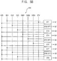
- the first clock signal CK1 and the first inverted clock signal CKB1 are deactivated in a P-th frame so that the first group of stages ST1, ST4 and ST7 in FIG. 5A are deactivated. Since the first group of stages ST1, ST4 and ST7 are deactivated, gate signals G1, G4 and G7 applied to the first group of gate lines GL1, GL4 and GL7 are deactivated. Since the gate signals G1, G4 and G7 applied to the first group of gate lines GL1, GL4 and GL7 are deactivated, data voltages are not charged to subpixels in the subpixel rows connected to the first group of gate lines GL1, GL4 and GL7. When the data voltages are not charged to the subpixels in the subpixel rows connected to the first group of gate lines GL1, GL4 and GL7, the data voltages of the previous frame may be maintained at the subpixels.
- the second clock signal CK2 has a rising edge of a first time and has a second pulse width TB
- the third clock signal CK3 has a rising edge of a second time which is later than the first time by 1/2 of the second pulse width TB and has the second pulse width TB.
- the second inverted clock signal CKB2 may be an inverted signal of the second clock signal CK2.
- the third inverted clock signal CKB3 may be an inverted signal of the third clock signal CK3.
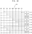
- the third clock signal CK3 and the third inverted clock signal CKB3 are deactivated in a (P+2)-th frame so that the third group of stages ST3, ST6 and ST9 in FIG. 5C are deactivated.
- gate signals G3, G6 and G9 applied to the third group of gate lines GL3, GL6 and GL9 are deactivated.
- the gate signals G3, G6 and G9 applied to the third group of gate lines GL3, GL6 and GL9 are deactivated, data voltages are not charged to subpixels in the subpixel rows connected to the third group of gate lines GL3, GL6 and GL9.
- the data voltages of the previous frame may be maintained at the subpixels.
- the display panel is driven in a (P+3)-th frame same as in the P-th frame.
- the driving method is repeated in a cycle of three frames.
- the timing controller 200 includes an image compensating part 220, a mode determining part 240 and a signal generating part 260.
- the image compensating part 220 receives the input image data IMG.
- the image compensating part 220 may receive the input image data IMG[P] of a present frame and the input image data IMG[P-1] of a previous frame.
- the image compensating part 220 compensates grayscale values of the input image data IMG.
- the image compensating part 220 may include an adaptive color correction part and a dynamic capacitance compensation part.
- the adaptive color correction part receives the grayscale values of the input image data IMG[P] and operates an adaptive color correction to the grayscale values of the input image data IMG[P].
- the adaptive color correction part may compensate the grayscale values using a gamma curve.
- the dynamic capacitance compensation part operates a dynamic capacitance compensation which compensates the grayscale values of the present frame data IMG[P] using the previous frame data IMG[P-1] and the present frame data IMG[P].
- the image compensating part 220 compensates the grayscale values of the input image data IMG[P] and generates the data signal DATA[P] by rearranging the input image data IMG[P] to correspond to a data type of the data driver 500.
- the data signal DATA may be a digital signal.
- the image compensating part 220 outputs the data signal DATA to the data driver 500.
- the mode determining part 240 receives the input image data IMG.
- the mode determining part 240 may receive the input image data IMG[P] of the present frame and the input image data IMG[P-1] of the previous frame.
- the mode determining part 240 may determine a driving mode MODE of the gate driver 300 based on the input image data IMG.
- the driving mode MODE may include a first mode (a normal driving mode) and a second mode (a "three line skip" mode).
- the gate signals applied to each of the gate lines of the display panel 100 may be activated in the P-th frame, the (P+1)-th frame and the (P+2)-th frame.
- the gate signals applied to the first group of gate lines of the display panel 100 may be deactivated in the P-th frame, the gate signals applied to the second group of gate lines of the display panel 100 may be deactivated in the (P+1)-th frame and the gate signals applied to the third group of gate lines of the display panel 100 may be deactivated in the (P+2)-th frame.
- the mode determining part 240 may determine the driving mode MODE based on a moving velocity of a pattern in the previous frame and the present frame.
- the mode determining part 240 may determine the driving mode MODE is the first mode. In contrast, when the moving velocity of the pattern in the previous frame and the present frame is relatively little, the mode determining part 240 may determine the driving mode MODE is the second mode.
- the signal generating part 260 receives the input control signal CONT and the driving mode MODE.
- the signal generating part 260 generates the first control signal CONT1 for controlling the driving timing of the gate driver 300 and the second control signal CONT2 for controlling the driving timing of the data driver 500 based on the input control signal CONT and the driving mode MODE.
- the signal generating part 260 may generate the first clock signal CK1, the second clock signal CK2, the third clock signal CK3, the first inverted clock signal CKB1, the second inverted clock signal CKB2, and the third inverted clock signal CKB3, as shown in FIGS. 8A , 8B and 8C .
- the signal generating part 260 outputs the first control signal CONT1 to the gate driver 300.
- the signal generating part 260 outputs the second control signal CONT2 to the data driver 500.
- the signal generating part 260 outputs the third control signal CONT3 to the gamma reference voltage generator 400.
- the gate signals applied to some of the gate lines are deactivated according to the frames, and a data charging time in a horizontal period may be reduced.
- the charging rate of the data voltage of the subpixel may be increased so that the display quality of the display panel 100 may be enhanced.
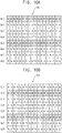
- FIG. 10A is a conceptual diagram illustrating a method of driving a display panel according to an exemplary embodiment of the present invention, during a P-th frame.
- FIG. 10B is a conceptual diagram illustrating a method of driving the display panel of FIG. 10A during a (P+1)-th frame.
- FIG. 10C is a conceptual diagram illustrating a method of driving the display panel of FIG. 10A during a (P+2)-th frame.
- FIG. 10D is a conceptual diagram illustrating a method of driving the display panel of FIG. 10A during a (P+3)-th frame.
- FIG. 10E is a conceptual diagram illustrating a method of driving the display panel of FIG. 10A during a (P+4)-th frame.
- the method of driving the display panel and the display apparatus may be substantially the same as the method of driving the display panel and the display apparatus discussed above with respect to FIGS. 1 to 9 except that the gate driver operates a "four line skip" driving in a cycle of four frames.
- the same reference numerals may be used to refer to the same or like parts as those described in the previous exemplary embodiment of FIGS. 1 to 9 and it may be assumed that any omitted description is similar to, or identical to, corresponding features that have been described above.
- the display panel 100 includes a plurality of subpixels disposed in a matrix form.
- the display panel 100 may include a first subpixel having a first color, a second subpixel having a second color, and a third subpixel having a third color.
- the first color may be red R.
- the second color may be green G.
- the third color may be blue B.
- the first subpixel having the first color R, the second subpixel having the second color G, and the third subpixel having the third color B are alternately disposed along a row direction and the subpixels having the same color are disposed along a column direction in the display panel 100.
- the display panel 100 is driven in "four line skip" driving.
- gate signals applied to a first group of gate lines are deactivated.
- gate signals applied to a second group of gate lines are deactivated.
- gate signals applied to a third group of gate lines are deactivated.
- gate signals applied to a fourth group of gate lines are deactivated.
- gate signals applied to the first group of gate lines are deactivated the same as during the P-th frame.
- the first group of gate lines may be (4M-3)-th gate lines.
- M is a positive integer.
- the first group of gate lines may include the first gate line GL1 and the fifth gate line GL5.
- the third group of gate lines may be (4M-1)-th gate lines.
- the third group of gate lines may include the third gate line GL3 and the seventh gate line GL7.
- the fourth group of gate lines may be 4M-th gate lines.
- the fourth group of gate lines may include the fourth gate line GL4 and the eighth gate line GL8.
- the number of the first group of gate lines may be less than a half of the number of all gate lines of the display panel 100.
- the number of the second group of gate lines may be less than a half of the number of all gate lines of the display panel 100.
- the number of the third group of gate lines may be less than a half of the number of all gate lines of the display panel 100.
- the number of the fourth group of gate lines may be less than a half of the number of all gate lines of the display panel 100.
- the number of the first group of gate lines may be substantially the same as the number of the second group of gate lines.
- the number of the first group of gate lines may be substantially the same as the number of the third group of gate lines.
- the number of the first group of gate lines may be substantially the same as the number of the fourth group of gate lines.
- the number of the first group of gate lines may be 1/4 of all gate lines of the display panel 100.
- the gate driver 300 operates the "four line skip" driving using the clock signal.
- the first group of the stages outputting the gate signals applied to the first group of gate lines are deactivated and the clock signal for generating the gate signals applied to the first group of gate lines may be deactivated.
- the pulse widths of the second clock signal CK2 and the second inverted clock signal CKB2, the third clock signal CK3, the third inverted clock signal CKB3, a fourth clock signal CK4, and the fourth inverted clock signal CKB4 may be increased compared to the pulse width TA in the normal driving in FIG. 7 .
- the number of the gate lines to be scanned is decreased by 3/4 so that the pulse widths of the second clock signal CK2, the second inverted clock signal CKB2, the third clock signal CK3, the third inverted clock signal CKB3, the fourth clock signal CK4, and the fourth inverted clock signal CKB4 may be 4/3 times the pulse width TA of the clock signal in the normal driving in FIG. 7 .
- the gate signals applied to some of the gate lines are deactivated according to the frames, and a data charging time in a horizontal period may be reduced.
- the charging rate of the data voltage of the subpixel may be increased so that the display quality of the display panel 100 may be enhanced.
- FIG. 11A is a conceptual diagram illustrating a method of driving a display panel according to an exemplary embodiment of the present invention, during a P-th frame.
- FIG. 11B is a conceptual diagram illustrating a method of driving the display panel of FIG. 11A during a (P+1)-th frame.
- FIG. 11C is a conceptual diagram illustrating a method of driving the display panel of FIG. 11A during a (P+2)-th frame.
- FIG. 11D is a conceptual diagram illustrating a method of driving the display panel of FIG. 11A during a (P+3)-th frame.
- FIG. 11E is a conceptual diagram illustrating a method of driving the display panel of FIG. 11A during a (P+4)-th frame.
- a method of driving the display panel and the display apparatus may be substantially the same as the method of driving the display panel and the display apparatus described above with respect to FIGS. 10A to 10E except that the gate driver operates a random "four line skip" driving in a cycle of four frames instead of the sequential "four line skip” driving in a cycle of four frames.
- the same reference numerals may be used to refer to the same or like parts as those previously described with reference to FIGS. 10A to 10E and any elements not described may be understood to be similar to or identical to corresponding elements that have previously been described.
- the display panel 100 includes a plurality of subpixels disposed in a matrix form.
- the display panel 100 may include a first subpixel having a first color, a second subpixel having a second color, and a third subpixel having a third color.
- the first color may be red R.
- the second color may be green G.
- the third color may be blue B.
- the first subpixel having the first color R, the second subpixel having the second color G, and the third subpixel having the third color B are alternately disposed along a row direction and the subpixels having the same color are disposed along a column direction in the display panel 100.
- the display panel 100 may be driven according to "four line skip" driving.
- gate signals applied to a second group of gate lines are deactivated.
- gate signals applied to a first group of gate lines are deactivated.
- gate signals applied to a fourth group of gate lines are deactivated.
- gate signals applied to a third group of gate lines are deactivated.
- gate signals applied to the second group of gate lines are deactivated the same as during the P-th frame.
- the first group of gate lines may be (4M-3)-th gate lines.
- M is a positive integer.
- the first group of gate lines may include the first gate line GL1 and the fifth gate line GL5.
- the second group of gate lines may be (4M-2)-th gate lines.
- the second group of gate lines may include the second gate line GL2 and the sixth gate line GL6.
- the third group of gate lines may be (4M-1)-th gate lines.
- the third group of gate lines may include the third gate line GL3 and the seventh gate line GL7.
- the fourth group of gate lines may be 4M-th gate lines.
- the fourth group of gate lines may include the fourth gate line GL4 and the eighth gate line GL8.
- the first to fourth groups of the gate lines are not sequentially deactivated but randomly deactivated.
- a possible display defect due to the sequential inactivation of the first to fourth groups of the gate lines may be prevented.
- the gate signals applied to some of the gate lines are deactivated according to the frames, a data charging time in a horizontal period may be reduced.
- the charging rate of the data voltage of the subpixel may be increased so that the display quality of the display panel 100 may be enhanced.
- FIG. 12A is a timing diagram illustrating the gate signal and the data voltage applied to the subpixel of the display panel 100, according to an exemplary embodiment of the present invention, when overdriving is not applied to the display panel 100.
- FIG. 12B is a timing diagram illustrating the gate signal and the data voltage applied to the subpixel of the display panel 100, according to an exemplary embodiment of the present invention, when overdriving is applied to the display panel 100.
- the method of driving the display panel and the display apparatus may be substantially the same as the method of driving the display panel and the display apparatus previously described with respect to FIGS. 1 to 9 except that the data voltage is overdriven in a previous frame of a skipped frame when the gate signal is skipped.
- the same reference numerals may be used to refer to the same or like parts as those previously described with reference to FIGS. 1 to 9 and any omitted explanation may be assumed to be the same as previously described.
- the gate signal corresponding to a first subpixel is skipped in a (P+1)-th frame.
- a data voltage D[P] corresponding to a target grayscale value GT is applied to the first subpixel in response to a gate signal G[P] in a P-th frame.
- the data voltage D[P] charged at the first subpixel is gradually discharged as time passes.
- the gate signal G[P+1] corresponding to the first subpixel in the (P+1)-th frame is skipped so that the data voltage D[P+1] is not applied to the first subpixel in the (P+1)-th frame.
- the data voltage having the overdriving grayscale value GO greater than the target grayscale value GT may be applied to the subpixels of the subpixel rows connected to the first group of gate lines in the (P-1)-th frame.
- the data voltage having the overdriving grayscale value GO greater than the target grayscale value GT may be applied to the subpixels of the subpixel rows connected to the second group of gate lines in the P-th frame.
- the method of applying the data voltage having the overdriving grayscale value in the previous frame of the skipped frame in the "gate line skip” driving may be applied to the exemplary embodiment of the "three line sequential skip” driving explained above with reference to FIGS. 3A to 3D , the exemplary embodiment of the four line sequential skip driving explained above with reference to FIGS. 10A to 10E , and the exemplary embodiment of the four line random skip driving explained above with reference to FIGS. 11A to 11E .
- the gate signals applied to some of the gate lines are deactivated by frames, a data charging time in a horizontal period may be reduced.
- the charging rate of the data voltage of the subpixel may be increased so that the display quality of the display panel 100 may be enhanced.
- the overdriving grayscale value GO which is greater than the target grayscale value GT, may be applied to the subpixel connected to the gate line which is skipped in the previous frame.
- the deterioration of the display quality due to the discharge of the data voltage may be prevented.
- FIG. 13 is a conceptual diagram illustrating a display panel 100A according to an exemplary embodiment of the present invention.
- FIG. 14A is a conceptual diagram illustrating a method of driving the display panel 100A of FIG. 13 during a P-th frame.
- FIG. 14B is a conceptual diagram illustrating a method of driving the display panel 100A of FIG. 13 during a (P+1)-th frame.
- FIG. 14C is a conceptual diagram illustrating a method of driving the display panel 100A of FIG. 13 during a (P+2)-th frame.
- FIG. 14D is a conceptual diagram illustrating a method of driving the display panel 100A of FIG. 13 during a (P+3)-th frame.
- FIG. 14E is a conceptual diagram illustrating a method of driving the display panel 100A of FIG.
- FIG. 14F is a conceptual diagram illustrating a method of driving the display panel 100A of FIG. 13 during a (P+5)-th frame.
- FIG. 14G is a conceptual diagram illustrating a method of driving the display panel 100A of FIG. 13 during a (P+6)-th frame.
- the method of driving the display panel and the display apparatus may be substantially the same as the method of driving the display panel and the display apparatus described above with reference to FIGS. 1 to 9 except for the structure of the display panel and except that the gate driver operates a "six line skip" driving in a cycle of six frames.
- the same reference numerals may be used to refer to the same or like parts as those described in the previous exemplary embodiment of FIGS. 1 to 9 and any omitted description may be understood to be similar to or identical to corresponding elements that have been previously described.
- the display panel 100A includes a plurality of subpixels disposed in a matrix form.
- the display panel 100A may include a first subpixel having a first color, a second subpixel having a second color, and a third subpixel having a third color.
- the first color may be red R.
- the second color may be green G.
- the third color may be blue B.
- the subpixels having the same color are disposed along a row direction and the first subpixel having the first color R, the second subpixel having the second color G, and the third subpixel having the third color B are alternately disposed along a column direction in the display panel 100A.
- the display panel 100A is driven in "six line skip" driving.
- gate signals applied to a first group of gate lines are deactivated.
- gate signals applied to a second group of gate lines are deactivated.
- gate signals applied to a third group of gate lines are deactivated.
- gate signals applied to a fourth group of gate lines are deactivated.
- gate signals applied to a fifth group of gate lines are deactivated.
- gate signals applied to a sixth group of gate lines are deactivated.
- gate signals applied to the first group of gate lines are deactivated the same as during the P-th frame.
- the first group of gate lines may be (6M-5)-th gate lines.
- M is a positive integer.
- the first group of gate lines may include the first gate line GL1 and the seventh gate line GL7.
- the second group of gate lines may be (6M-4)-th gate lines.
- the second group of gate lines may include the second gate line GL2 and the eighth gate line GL8.
- the third group of gate lines may be (6M-3)-th gate lines.
- the third group of gate lines may include the third gate line GL3 and the ninth gate line GL9.
- the fourth group of gate lines may be (6M-2)-th gate lines.
- the fourth group of gate lines may include the fourth gate line GL4 and the tenth gate line GL10.
- the fifth group of gate lines may be (6M-1)-th gate lines.
- the fifth group of gate lines may include the fifth gate line GL5 and the eleventh gate line GL11.
- the sixth group of gate lines may be 6M-th gate lines.
- the sixth group of gate lines may include the sixth gate line GL6 and the twelfth gate line GL12.
- the number of the first group of gate lines may be less than a half of the number of all gate lines of the display panel 100A.
- the number of the second group of gate lines may be less than a half of the number of all gate lines of the display panel 100A.
- the number of the third group of gate lines may be less than a half of the number of all gate lines of the display panel 100A.
- the number of the fourth group of gate lines may be less than a half of the number of all gate lines of the display panel 100A.
- the number of the fifth group of gate lines may be less than a half of the number of all gate lines of the display panel 100A.
- the number of the sixth group of gate lines may be less than a half of the number of all gate lines of the display panel 100A.
- the number of the first group of gate lines, the number of the second group of gate lines, the number of the third group of gate lines, the number of the fourth group of gate lines, the number of the fifth group of gate lines and the number of the sixth group of gate lines may be substantially the same as one another.
- the number of the first group of gate lines may be 1/6 of all gate lines of the display panel 100A.
- the gate driver 300 operates the "six line skip" driving using the clock signal.
- the first group of the stages outputting the gate signals applied to the first group of gate lines are deactivated and the clock signal for generating the gate signals applied to the first group of gate lines may be deactivated.
- the number of the gate lines to be scanned is decreased by 5/6 so that the pulse widths of the second clock signal CK2 and the second inverted clock signal CKB2, the third clock signal CK3, the third inverted clock signal CKB3, the fourth clock signal CK4, the fourth inverted clock signal CKB4, the fifth clock signal CK5, the fifth inverted clock signal CKB5, the sixth clock signal CK6 and the sixth inverted clock signal CKB6 may be 6/5 times the pulse width TA of the clock signal in the normal driving in FIG. 7 .
- Each of the subpixels of the display panel 100A which are deactivated in the P-th frame may be red subpixels.
- Each of the subpixels of the display panel 100A which are deactivated in the (P+1)-th frame may be green subpixels.
- Each of the subpixels of the display panel 100A which are deactivated in the (P+2)-th frame may be blue subpixels. Accordingly, the display defect of color loss may be generated.
- the method of applying the data voltage having the overdriving grayscale value in the previous frame of the skipped frame in the "gate line skip" driving explained above with reference to FIGS. 12A and 12B may be applied to the "six line skip" driving of the instant display panel.
- the display defect of color loss may be prevented.
- the gate signals applied to some of the gate lines are deactivated by frames, a data charging time in a horizontal period may be reduced.
- the charging rate of the data voltage of the subpixel may be increased so that the display quality of the display panel 100A may be enhanced.
- the overdriving grayscale value GO greater than the target grayscale value GT may be applied to the subpixel connected to the gate line which is skipped in the previous frame.
- the deterioration of the display quality due to the discharge of the data voltage may be prevented.
- FIG. 15A is a conceptual diagram illustrating a method of driving the display panel 100A, according to an exemplary embodiment of the present invention, during a P-th frame.
- FIG. 15B is a conceptual diagram illustrating a method of driving the display panel 100A of FIG. 15A during a (P+1)-th frame.
- FIG. 15C is a conceptual diagram illustrating a method of driving the display panel 100A of FIG. 15A during a (P+2)-th frame.
- FIG. 15D is a conceptual diagram illustrating a method of driving the display panel 100A of FIG. 15A during a (P+3)-th frame.
- the method of driving the display panel and the display apparatus may be substantially the same as the method of driving the display panel and the display apparatus described above with reference to FIGS. 13 to 14G except that the 2 adjacent gate lines are simultaneously skipped in a cycle of three frames.
- the same reference numerals may be used to refer to the same or like parts as those described above with reference to FIGS. 13 to 14G and any omitted description may be understood to be identical to, or similar to corresponding elements that have been previously described.
- the subpixels having the same color are disposed along a row direction and the first subpixel having the first color R, the second subpixel having the second color G, and the third subpixel having the third color B are alternately disposed along a column direction in the display panel 100A.
- Two adjacent gate lines of the display panel 100A form a pair and the display panel 100A is driven in "six line skip" driving.
- gate signals applied to a first group of gate lines are deactivated.
- gate signals applied to a second group of gate lines are deactivated.
- gate signals applied to a third group of gate lines are deactivated.
- gate signals applied to the first group of gate lines are deactivated the same as during the P-th frame.
- the first group of gate lines may include (6M-5)-th gate lines and (6M-4)-th gate lines.
- M is a positive integer.
- the first group of gate lines may include the first gate line GL1, the second gate line GL2, the seventh gate line GL7, and the eighth gate line GL8.
- the second group of gate lines may include (6M-3)-th gate lines and (6M-2)-th gate lines.
- the second group of gate lines may include the third gate line GL3, the fourth gate line GL4, the ninth gate line GL9, and the tenth gate line GL10.
- the third group of gate lines may include (6M-1)-th gate lines and 6M-th gate lines.
- the third group of gate lines may include the fifth gate line GL5, the sixth gate line GL6, the eleventh gate line GL11, and the twelfth gate line GL12.
- the number of the first group of gate lines may be less than a half of the number of all gate lines of the display panel 100A.
- the number of the second group of gate lines may be less than a half of the number of all gate lines of the display panel 100A.
- the number of the third group of gate lines may be less than a half of the number of all gate lines of the display panel 100A.
- the number of the first group of gate lines, the number of the second group of gate lines, and the number of the third group of gate lines may be substantially the same as one another.
- the subpixels of the display panel 100A which are deactivated in the P-th frame may be red and green subpixels
- the subpixels of the display panel 100A which are deactivated in the (P+1)-th frame may be blue and red subpixels
- the subpixels of the display panel 100A which are deactivated in the (P+2)-th frame may be green and blue subpixels so that the display defect of color loss may be generated.
- the method of applying the data voltage having the overdriving grayscale value in the previous frame of the skipped frame in the "gate line skip" driving explained above with reference to FIGS. 12A and 12B may be applied to the "two line pair skip" driving described above.
- the display defect of color loss may be prevented.
- the gate signals applied to some of the gate lines are deactivated according to the frames, a data charging time in a horizontal period may be reduced.
- the charging rate of the data voltage of the subpixel may be increased so that the display quality of the display panel 100 may be enhanced.
- the overdriving grayscale value GO greater than the target grayscale value GT may be applied to the subpixel connected to the gate line which is skipped in the previous frame.
- the deterioration of the display quality due to the discharge of the data voltage may be prevented.
- the charging rate of the data voltage applied to the subpixel may be increased so that the display quality of the display panel may be enhanced.
Landscapes
- Engineering & Computer Science (AREA)
- Physics & Mathematics (AREA)
- Computer Hardware Design (AREA)
- General Physics & Mathematics (AREA)
- Theoretical Computer Science (AREA)
- Chemical & Material Sciences (AREA)
- Crystallography & Structural Chemistry (AREA)
- Control Of Indicators Other Than Cathode Ray Tubes (AREA)
- Liquid Crystal Display Device Control (AREA)
- Liquid Crystal (AREA)
Description
- Exemplary embodiments of the present inventive concept relate to a display apparatus, and more particularly, exemplary embodiments of the present inventive concept relate to a method of driving a display panel and a display apparatus for performing the method.
- Generally, a display apparatus includes a display panel and a display panel driver. The display panel includes a plurality of gate lines, a plurality of data lines and a plurality of subpixels. The display panel driver includes a gate driver providing gate signals to the gate lines and a data driver providing data voltages to the data lines.
- As a size of the display panel increases and a driving frequency of the display panel increases, a charging time required to charge the subpixels to the data voltage may decrease.
- A display apparatus includes a display panel having a plurality of gate lines, a plurality of data lines, and a plurality of subpixels. Each of the plurality of subpixels includes a subpixel electrode connected to one of the plurality of gate lines and one of the plurality of data lines through a switching element. A gate driver is configured to output a plurality of gate signals to the plurality of gate lines and to deactivate at least one of the plurality of gate signals in a P-th frame. A data driver is configured to output a plurality of data voltages to the plurality of data lines. Here, P is a positive integer.
- A method of driving a display panel includes deactivating at least one gate signal of a plurality of gate signals in a P-th frame. Activated gate signals of the plurality of gate signals are applied to a plurality of gate lines. A plurality of data voltages is applied to a plurality of data lines. An image is displayed based on the plurality of gate signals and the plurality of data voltages. Here, P is a positive integer.
- The above and other features and aspects of the present inventive concept will become more apparent by describing in detailed exemplary embodiments thereof with reference to the accompanying drawings, in which:
-
FIG. 1 is a block diagram illustrating a display apparatus, according to an exemplary embodiment of the present inventive concept; -
FIG. 2 is a conceptual diagram illustrating a display panel ofFIG. 1 , according to an exemplary embodiment of the present inventive concept; -
FIG. 3A is a conceptual diagram illustrating a method of driving the display panel ofFIG. 1 during a P-th frame, according to an exemplary embodiment of the present inventive concept; -
FIG. 3B is a conceptual diagram illustrating a method of driving the display panel ofFIG. 1 during a (P+1)-th frame, according to an exemplary embodiment of the present inventive concept; -
FIG. 3C is a conceptual diagram illustrating a method of driving the display panel ofFIG. 1 during a (P+2)-th frame, according to an exemplary embodiment of the present inventive concept; -
FIG. 3D is a conceptual diagram illustrating a method of driving the display panel ofFIG. 1 during a (P+3)-th frame, according to an exemplary embodiment of the present inventive concept; -
FIG. 4 is a conceptual diagram illustrating a gate driver ofFIG. 1 according to an exemplary embodiment of the present inventive concept; -
FIG. 5A is a conceptual diagram illustrating an operation of the gate driver ofFIG. 4 during the P-th frame, according to an exemplary embodiment of the present inventive concept; -
FIG. 5B is a conceptual diagram illustrating an operation of the gate driver ofFIG. 4 during the (P+1)-th frame, according to an exemplary embodiment of the present inventive concept; -
FIG. 5C is a conceptual diagram illustrating an operation of the gate driver ofFIG. 4 during the (P+2)-th frame, according to an exemplary embodiment of the present inventive concept; -
FIG. 5D is a conceptual diagram illustrating an operation of the gate driver ofFIG. 4 during the (P+3)-th frame, according to an exemplary embodiment of the present inventive concept; -
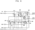
FIG. 6 is a circuit diagram illustrating an N-th stage of the gate driver ofFIG. 4 , according to an exemplary embodiment of the present inventive concept; -
FIG. 7 is a timing diagram illustrating clock signals applied to the gate driver ofFIG. 1 when the gate driver ofFIG. 1 operates normal driving, according to an exemplary embodiment of the present inventive concept; -
FIG. 8A is a timing diagram illustrating clock signals applied to the gate driver ofFIG. 1 during the P-th frame when the gate driver ofFIG. 1 operates "three line skip" driving, according to an exemplary embodiment of the present inventive concept; -
FIG. 8B is a timing diagram illustrating clock signals applied to the gate driver ofFIG. 1 during the (P+1)-th frame when the gate driver ofFIG. 1 operates the "three line skip" driving, according to an exemplary embodiment of the present inventive concept; -
FIG. 8C is a timing diagram illustrating clock signals applied to the gate driver ofFIG. 1 during the (P+2)-th frame when the gate driver ofFIG. 1 operates the "three line skip" driving, according to an exemplary embodiment of the present inventive concept; -
FIG. 8D is a timing diagram illustrating clock signals applied to the gate driver ofFIG. 1 during the (P+3)-th frame when the gate driver ofFIG. 1 operates the "three line skip" driving, according to an exemplary embodiment of the present inventive concept; -
FIG. 9 is a block diagram illustrating a timing controller ofFIG. 1 , according to an exemplary embodiment of the present inventive concept; -
FIG. 10A is a conceptual diagram illustrating a method of driving a display panel according to an exemplary embodiment during a P-th frame, according to an exemplary embodiment of the present inventive concept; -
FIG. 10B is a conceptual diagram illustrating a method of driving the display panel ofFIG. 10A during a (P+1)-th frame, according to an exemplary embodiment of the present inventive concept; -
FIG. 10C is a conceptual diagram illustrating a method of driving the display panel ofFIG. 10A during a (P+2)-th frame, according to an exemplary embodiment of the present inventive concept; -
FIG. 10D is a conceptual diagram illustrating a method of driving the display panel ofFIG. 10A during a (P+3)-th frame, according to an exemplary embodiment of the present inventive concept; -
FIG. 10E is a conceptual diagram illustrating a method of driving the display panel ofFIG. 10A during a (P+4)-th frame, according to an exemplary embodiment of the present inventive concept; -
FIG. 11A is a conceptual diagram illustrating a method of driving a display panel according to an exemplary embodiment during a P-th frame, according to an exemplary embodiment of the present inventive concept; -
FIG. 11B is a conceptual diagram illustrating a method of driving the display panel ofFIG. 11A during a (P+1)-th frame, according to an exemplary embodiment of the present inventive concept; -
FIG. 11C is a conceptual diagram illustrating a method of driving the display panel ofFIG. 11A during a (P+2)-th frame, according to an exemplary embodiment of the present inventive concept; -
FIG. 11D is a conceptual diagram illustrating a method of driving the display panel ofFIG. 11A during a (P+3)-th frame, according to an exemplary embodiment of the present inventive concept; -
FIG. 11E is a conceptual diagram illustrating a method of driving the display panel ofFIG. 11A during a (P+4)-th frame, according to an exemplary embodiment of the present inventive concept; -
FIG. 12A is a timing diagram illustrating a gate signal and a data voltage applied to a subpixel of a display panel, according to an exemplary embodiment of the present inventive concept, when overdriving is not applied to the display panel; -
FIG. 12B is a timing diagram illustrating the gate signal and the data voltage applied to the subpixel of the display panel, according to an exemplary embodiment of the present inventive concept, when overdriving is applied to the display panel; -
FIG. 13 is a conceptual diagram illustrating a display panel according to an exemplary embodiment of the present inventive concept; -
FIG. 14A is a conceptual diagram illustrating a method of driving the display panel ofFIG. 13 during a P-th frame, according to an exemplary embodiment of the present inventive concept; -
FIG. 14B is a conceptual diagram illustrating a method of driving the display panel ofFIG. 13 during a (P+1)-th frame, according to an exemplary embodiment of the present inventive concept; -
FIG. 14C is a conceptual diagram illustrating a method of driving the display panel ofFIG. 13 during a (P+2)-th frame, according to an exemplary embodiment of the present inventive concept; -
FIG. 14D is a conceptual diagram illustrating a method of driving the display panel ofFIG. 13 during a (P+3)-th frame, according to an exemplary embodiment of the present inventive concept; -
FIG. 14E is a conceptual diagram illustrating a method of driving the display panel ofFIG. 13 during a (P+4)-th frame, according to an exemplary embodiment of the present inventive concept; -
FIG. 14F is a conceptual diagram illustrating a method of driving the display panel ofFIG. 13 during a (P+5)-th frame, according to an exemplary embodiment of the present inventive concept; -
FIG. 14G is a conceptual diagram illustrating a method of driving the display panel ofFIG. 13 during a (P+6)-th frame, according to an exemplary embodiment of the present inventive concept; -
FIG. 15A is a conceptual diagram illustrating a method of driving a display panel, according to an exemplary embodiment of the present inventive concept, during a P-th frame; -
FIG. 15B is a conceptual diagram illustrating a method of driving the display panel ofFIG. 15A during a (P+1)-th frame, according to an exemplary embodiment of the present inventive concept; -
FIG. 15C is a conceptual diagram illustrating a method of driving the display panel ofFIG. 15A during a (P+2)-th frame, according to an exemplary embodiment of the present inventive concept; and -
FIG. 15D is a conceptual diagram illustrating a method of driving the display panel ofFIG. 15A during a (P+3)-th frame, according to an exemplary embodiment of the present inventive concept. - Hereinafter, exemplary embodiments of the present inventive concept will be explained in detail with reference to the accompanying drawings.
-
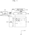
FIG. 1 is a block diagram illustrating a display apparatus, according to an exemplary embodiment of the present inventive concept. - Referring to
FIG. 1 , the display apparatus includes adisplay panel 100 and a display panel driver. The display panel driver includes atiming controller 200, agate driver 300, a gammareference voltage generator 400 and adata driver 500. - The
display panel 100 has a display region on which an image is displayed and a peripheral region, on which an image is not displayed, adjacent to the display region. - The
display panel 100 includes a plurality of gate lines GL, a plurality of data lines DL, and a plurality of subpixels SP connected to the gate lines GL and the data lines DL. The gate lines GL extend in a first direction D1 and the data lines DL extend in a second direction D2 crossing the first direction D1. - Each subpixel SP includes a switching element TR and a subpixel electrode SPE connected to the switching element TR. The subpixel electrode SPE is connected to one of the gate lines GL and one of the data lines DL through the switching element TR. Each subpixel SP may further include a liquid crystal capacitor, and a storage capacitor. The liquid crystal capacitor and the storage capacitor are electrically connected to the switching element TR. The subpixels SP may be disposed in a matrix form.
- The
display panel 100 is further described below with reference toFIGS. 2 to 3D . - The
timing controller 200 receives input image data IMG and an input control signal CONT from an external source. The input image data IMG may include red image data, green image data, and blue image data. The input control signal CONT may include a master clock signal and a data enable signal. The input control signal CONT may further include a vertical synchronizing signal and a horizontal synchronizing signal. - The
timing controller 200 generates a first control signal CONT1, a second control signal CONT2, a third control signal CONT3, and a data signal DATA based on the input image data IMG and the input control signal CONT. - The
timing controller 200 generates the first control signal CONT1 for controlling an operation of thegate driver 300 based on the input control signal CONT, and outputs the first control signal CONT1 to thegate driver 300. The first control signal CONT1 may include a driving mode signal. The first control signal CONT1 may further include a vertical start signal and a gate clock signal. - The
timing controller 200 generates the second control signal CONT2 for controlling an operation of thedata driver 500 based on the input control signal CONT, and outputs the second control signal CONT2 to thedata driver 500. The second control signal CONT2 may include the driving mode signal. The second control signal CONT2 may further include a horizontal start signal and a load signal. - The
timing controller 200 generates the data signal DATA based on the input image data IMG. Thetiming controller 200 outputs the data signal DATA to thedata driver 500. - The
timing controller 200 generates the third control signal CONT3 for controlling an operation of the gammareference voltage generator 400 based on the input control signal CONT, and outputs the third control signal CONT3 to the gammareference voltage generator 400. - A structure and an operation of the
timing controller 200 are further explained below referring toFIGS. 7 to 9 . - The
gate driver 300 generates gate signals for driving the gate lines GL in response to the first control signal CONT1 received from thetiming controller 200. Thegate driver 300 sequentially outputs the gate signals to the gate lines GL. - The
gate driver 300 may deactivate at least one gate signal during a P-th frame. Herein, P is a positive integer. - The
gate driver 300 may include a plurality of stages. The stages may be connected to at least one clock line providing a clock signal. The clock signal applied to the stage, which is connected to the gate line having the deactivated gate signal, may be deactivated. - The gate signal, which is deactivated during the P-th frame, may be activated during a (P+K)-th frame. In addition, at least one gate signal, which is activated during the P-th frame, may be deactivated during the (P+K)-th frame. Herein, K is a positive integer. As explained above, the gate signal that is deactivated changes according to a frame so that a deactivated line in the
display panel 100 might not be recognized by an observer. - A structure and an operation of the
gate driver 300 are further explained below with reference toFIGS. 4 to 6 . - The gamma
reference voltage generator 400 generates a gamma reference voltage VGREF in response to the third control signal CONT3 received from thetiming controller 200. The gammareference voltage generator 400 provides the gamma reference voltage VGREF to thedata driver 500. The gamma reference voltage VGREF has a value corresponding to a level of the data signal DATA. - According to an exemplary embodiment of the present invention, the gamma
reference voltage generator 400 may be disposed in thetiming controller 200, or in thedata driver 500. - The
data driver 500 receives the second control signal CONT2 and the data signal DATA from thetiming controller 200, and receives the gamma reference voltages VGREF from the gammareference voltage generator 400. Thedata driver 500 converts the data signal DATA into analog data voltages using the gamma reference voltages VGREF. Thedata driver 500 outputs the data voltages to the data lines DL. -
FIG. 2 is a conceptual diagram illustrating thedisplay panel 100 ofFIG. 1 .FIG. 3A is a conceptual diagram illustrating a method of driving thedisplay panel 100 ofFIG. 1 during a P-th frame.FIG. 3B is a conceptual diagram illustrating a method of driving thedisplay panel 100 ofFIG. 1 during a (P+1)-th frame.FIG. 3C is a conceptual diagram illustrating a method of driving thedisplay panel 100 ofFIG. 1 during a (P+2)-th frame.FIG. 3D is a conceptual diagram illustrating a method of driving thedisplay panel 100 ofFIG. 1 during a (P+3)-th frame. InFIGS. 2 to 3D , only a part of thedisplay panel 100 is shown for convenience of explanation. - Referring to
FIGS. 1 to 3D , thedisplay panel 100 includes a plurality of subpixels disposed in a matrix form. Thedisplay panel 100 may include a first subpixel having a first color, a second subpixel having a second color, and a third subpixel having a third color. Together, these three sub-pixels may be said to form a pixel. For example, the first color may be red R. For example, the second color may be green G. For example, the third color may be blue B. However, other combinations of sub-pixels may be used. - According to an exemplary embodiment of the present invention, the first subpixel having the first color R, the second subpixel having the second color G and the third subpixel having the third color B are alternately disposed along a row direction and the subpixels having the same colors are disposed along a column direction in the
display panel 100. - In the
display panel 100, a first subpixel row is connected to a first gate line GL1, a second subpixel row is connected to a second gate line GL2, a third subpixel row is connected to a third gate line GL3, a fourth subpixel row is connected to a fourth gate line GL4, a fifth subpixel row is connected to a fifth gate line GL5 and a sixth subpixel row is connected to a sixth gate line GL6. - According to an exemplary embodiment of the present invention, the
display panel 100 is driven in "three line skip" driving. This may mean that every 3rd gate line is deactivated at each frame. According to this driving approach, during the P-th frame, gate signals applied to a first group of gate lines are deactivated. During the (P+1)-th frame, gate signals applied to a second group of gate lines are deactivated. During the (P+2)-th frame, gate signals applied to a third group of gate lines are deactivated. - For example, the first group of gate lines may be (3M-2)-th gate lines. Herein, M is a positive integer. The first group of gate lines may include the first gate line GL1 and the fourth gate line GL4.
- For example, the second group of gate lines may be (3M-1)-th gate lines. The second group of gate lines may include the second gate line GL2 and the fifth gate line GL5.
- For example, the third group of gate lines may be 3M-th gate lines. The third group of gate lines may include the third gate line GL3 and the sixth gate line GL6.
- The number of the first group of gate lines may be less than a half of the number of all gate lines of the
display panel 100. The number of the second group of gate lines may be less than a half of the number of all gate lines of thedisplay panel 100. The number of the third group of gate lines may be less than a half of the number of all gate lines of thedisplay panel 100. For example, the number of the first group of gate lines may be substantially the same as the number of the second group of gate lines. For example, the number of the first group of gate lines may be substantially the same as the number of the third group of gate lines. - According to an exemplary embodiment of the present invention, the number of the first group of gate lines may be 1/3 of all gate lines of the
display panel 100. -
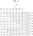
FIG. 4 is a conceptual diagram illustrating thegate driver 300 ofFIG. 1 .FIG. 5A is a conceptual diagram illustrating an operation of thegate driver 300 ofFIG. 4 during the P-th frame.FIG. 5B is a conceptual diagram illustrating an operation of thegate driver 300 ofFIG. 4 during the (P+1)-th frame.FIG. 5C is a conceptual diagram illustrating an operation of thegate driver 300 ofFIG. 4 during the (P+2)-th frame.FIG. 5D is a conceptual diagram illustrating an operation of thegate driver 300 ofFIG. 4 during the (P+3)-th frame.FIG. 6 is a circuit diagram illustrating an N-th stage of thegate driver 300 ofFIG. 4 . Herein, N is a positive integer. - Referring to
FIGS. 1 to 6 , thegate driver 300 includes a plurality of stages ST1 to ST9. InFIGS. 4 to 5D , only a part of the stages of thegate driver 300 is shown for convenience of explanation. The number of the stages may correspond to the number of the gate lines GL of thedisplay panel 100. - A first stage ST1 of the
gate driver 300 outputs a first gate signal G1 to the first gate line GL1. A second stage ST2 of thegate driver 300 outputs a second gate signal G2 to the second gate line GL2. A third stage ST3 of thegate driver 300 outputs a third gate signal G3 to the third gate line GL3. A fourth stage ST4 of thegate driver 300 outputs a fourth gate signal G4 to the fourth gate line GL4. A fifth stage ST5 of thegate driver 300 outputs a fifth gate signal G5 to the fifth gate line GL5. A sixth stage ST6 of thegate driver 300 outputs a sixth gate signal G6 to the sixth gate line GL6. - All stages of the
gate driver 300 receive a power voltage VSS. The power voltage VSS may include a first off voltage VSS1 and a second off voltage VSS2. - A (6M-5)-th stage (e.g. a first stage, a seventh stage, a thirteenth stage, ...) of the
gate driver 300 outputs the gate signal based on a first clock signal CK1. A (6M-4)-th stage (e.g. a second stage, an eighth stage, a fourteenth stage, ...) of thegate driver 300 outputs the gate signal based on a second clock signal CK2. A (6M-3)-th stage (e.g. a third stage, a ninth stage, a fifteenth stage, ...) of thegate driver 300 outputs the gate signal based on a third clock signal CK3. A (6M-2)-th stage (e.g. a fourth stage, a tenth stage, a sixteenth stage, ...) of thegate driver 300 outputs the gate signal based on a first inverted clock signal CKB1. A (6M-1)-th stage (e.g. a fifth stage, an eleventh stage, a seventeenth stage, ...) of thegate driver 300 outputs the gate signal based on a second inverted clock signal CKB2. A 6M-th stage (e.g. a sixth stage, a twelfth stage, an eighteenth stage, ...) of thegate driver 300 outputs the gate signal based on a third inverted clock signal CKB3. - According to an exemplary embodiment of the present invention, the
gate driver 300 operates the "three line skip" driving, thegate driver 300 may output the gate signals using three pairs CK1, CK2, CK3, CKB1, CKB2 and CKB3 of the clock signals. - In
FIG. 5A , a first group of stages ST1, ST4 and ST7 connected to the first group of gate lines may be deactivated during the P-th frame. The first clock signal CK1 and the first inverted clock signal CKB1 that generate the gate signals applied to the first group of gate lines may be deactivated during the P-th frame. - In
FIG. 5B , a second group of stages ST2, ST5 and ST8 connected to the second group of gate lines may be deactivated during the (P+1)-th frame. The second clock signal CK2 and the second inverted clock signal CKB2 that generate the gate signals applied to the second group of gate lines may be deactivated during the (P+1)-th frame. - In
FIG. 5C , a third group of stages ST3, ST6 and ST9 connected to the third group of gate lines may be deactivated during the (P+2)-th frame. The third clock signal CK3 and the third inverted clock signal CKB3 that generate the gate signals applied to the third group of gate lines may be deactivated during the (P+2)-th frame. - In
FIG. 5D , the first group of stages ST1, ST4 and ST7 connected to the first group of gate lines may be deactivated during the (P+3)-th frame, as is done during the P-th frame. The first clock signal CK1 and the first inverted clock signal CKB1 that generate the gate signals applied to the first group of gate lines may be deactivated during the (P+3)-th frame. - According to an exemplary embodiment of the present invention, the first group of stages ST1, ST4 and ST7, the second group of stages ST2, ST5 and ST8 and the third group of stages ST3, ST6 and ST9 are sequentially deactivated in a cycle of three frames.
-
FIG. 6 is an exemplary circuit diagram of the N-th stage of thegate driver 300 according to an exemplary embodiment of the present invention. The N-th stage of thegate driver 300 receives a clock signal CK, the first off voltage VSS1 and the second off voltage VSS2. Herein the clock signal CK may be the first clock signal CK1, the second clock signal CK2, the third clock signal CK3, the first inverted clock signal CKB1, the second inverted clock signal CKB2, or the third inverted clock signal CKB3, according to a position of the N-th stage. The N-th stage of thegate driver 300 outputs the gate signal G(N). - The clock signal CK is applied to a clock terminal. The first off voltage VSS1 is applied to a first off terminal. The second off voltage VSS2 is applied to a second off terminal. The gate signal G(N) is outputted at a gate output terminal.
- The clock signal CK is a square wave signal alternating between a high level and a low level. The high level of the clock signal CK may have a gate on voltage. The low level of the clock signal CK may have the second off voltage VSS2. For example, a duty ratio of the clock signal CK may be equal to 50%. Alternatively, the duty ratio of the clock signal CK may be less than 50%. For example, the gate on voltage may be between about 15V and about 20V
- The first off voltage VSS1 may be a direct-current (DC) voltage. The second off voltage VSS2 may be a direct-current (DC) voltage. The second off voltage VSS2 may be less than the first off voltage VSS1. For example, the first off voltage VSS1 may be about -5V. For example, the second off voltage VSS2 may be about -10V.
- The N-th stage outputs an N-th gate signal G(N) and an N-th carry signal CR(N) in response to an (N-1)-th carry signal CR(N-1) of an (N-1)-th stage which is a previous stage of the N-th stage. The N-th stage pulls down the gate signal G(N) to the first off voltage VSS1 in response to an (N+1)-th carry signal CR(N+1) of an (N+1)-th stage which is a next stage of the N-th stage. The vertical start signal STV may be applied to the first stage ST1 instead of the (N-1)-th stage.
- In the above-explained method, the first to last stages sequentially output the corresponding gate signals.
- The (N-1)-th carry signal CR(N-1) is applied to an (N-1)-th carry terminal. The (N+1)-th carry signal CR(N+1) is applied to an (N+1)-th carry terminal. The N-th carry signal CR(N) is applied to an N-th carry terminal.
- The N-th stage includes a pull up
control part 310, a chargingpart 320, a pull uppart 330, acarry part 340, an invertingpart 350, a first pull downpart 361, a second pull downpart 362, acarry stabilizing part 370, a first holdingpart 381, asecond holding part 382 and a third holding part 383. - The pull up
control part 310 includes a fourth transistor T4. The fourth transistor T4 includes a control electrode and an input electrode connected to the (N-1)-th carry terminal and an output electrode connected to a first node Q1. The first node Q1 is connected to a control electrode of the pull uppart 330. - The charging
part 320 includes a charging capacitor C1. The charging capacitor C1 includes a first electrode connected to the first node Q1 and a second electrode connected to the gate output terminal. - The pull up
part 330 includes a first transistor T1. The first transistor T1 includes a control electrode connected to the first node Q1, an input electrode connected to the clock terminal and an output electrode connected to the gate output terminal. - The
carry part 340 includes a fifteenth transistor T15 and a fourth capacitor C4. The fifteenth transistor T15 includes a control electrode connected to the first node Q1, an input electrode connected to the clock terminal and an output electrode connected to the N-th carry terminal. The fourth capacitor C4 includes a first electrode connected to the first node Q1 and a second electrode connected to the N-th carry terminal. - The inverting
part 350 includes a twelfth transistor T12, a seventh transistor T7, a thirteenth transistor T13, an eighth transistor T8, a second capacitor C2 and a third capacitor C3. The twelfth transistor T12 includes a control electrode and an input electrode which are connected to the clock terminal and an output electrode connected to a third node Q3. The seventh transistor T7 includes a control electrode connected to the third node Q3, an input electrode connected to the clock terminal and an output electrode connected to a second node Q2. The thirteenth transistor T13 includes a control electrode connected to the N-th carry terminal, an input electrode connected to the second off terminal and an output electrode connected to the third node Q3. The eighth transistor T8 includes a control electrode connected to the N-th carry terminal, an input electrode connected to the second off terminal and an output electrode connected to the second node Q2. The second capacitor C2 includes a first electrode connected to the clock terminal and a second terminal connected to the third node Q3. The third capacitor C3 includes a first electrode connected to the second node Q2 and a second electrode connected to the third node Q3. - Herein, the twelfth transistor T12 is a first inverting transistor. The seventh transistor T7 is a second inverting transistor. The thirteenth transistor T13 is a third inverting transistor. The eighth transistor T8 is a fourth inverting transistor.
- The first pull down
part 361 includes a ninth transistor T9. The ninth transistor T9 includes a control electrode connected to the (N+1)-th carry terminal, an input electrode connected to the second off terminal and an output electrode connected to the first node Q1. Alternatively, the first pull downpart 361 may include two or more switching elements connected to each other in series. - The second pull down
part 362 includes a second transistor T2. The second transistor T2 includes a control electrode connected to the (N+1)-th carry terminal, an input electrode connected to the first off terminal and an output electrode connected to the gate output terminal. - The
carry stabilizing part 370 includes a seventeenth transistor T17. The seventeenth transistor T17 includes a control electrode and an input electrode which are commonly connected to the (N+1)-th carry terminal and an output electrode connected to the N-th carry terminal. - The
carry stabilizing part 370 stably removes noise caused by a leaked current transmitted through a fourth transistor T4 of an (N+1)-th stage. - The
first holding part 381 includes a tenth transistor T10. The tenth transistor T10 includes a control electrode connected to the second node Q2, an input electrode connected to the second off terminal and an output electrode connected to the first node Q1. - The
second holding part 382 includes a third transistor T3. The third transistor T3 includes a control electrode connected to the second node Q2, an input electrode connected to the first off terminal and an output electrode connected to the gate output terminal. - The third holding part 383 includes an eleventh transistor T11. The eleventh transistor T11 includes a control electrode connected to the second node Q2, an input electrode connected to the second off terminal and an output electrode connected to the N-th carry terminal.
- In an exemplary embodiment of the present disclosure, the previous carry signal is not limited to the (N-1)-th carry signal. The previous carry signal may be any one of the carry signals of the previous stages. In addition, according to an exemplary embodiment of the present invention, the next carry signal is not limited to the (N+1)-th carry signal. The next carry signal may be any one of the carry signals of the next stages.
- In an exemplary embodiment of the present invention, the first, second, third, fourth, seventh, eighth, ninth, tenth, eleventh, twelfth, thirteenth, fifteenth, and seventeenth transistors may be oxide semiconductor transistors. Alternatively, the first, second, third, fourth, seventh, eighth, ninth, tenth, eleventh, twelfth, thirteenth, fifteenth, and seventeenth transistors may be amorphous silicon semiconductor transistor.
- The gate signal G(N) of the N-th stage is synchronized with the clock signal CK. The gate signal G(N) of the N-th stage has a high level corresponding to the N-th stage. The carry signal CR(N) of the N-th stage is synchronized with the clock signal CK. The carry signal CR(N) of the N-th stage has a high level corresponding to the N-th stage.
-
FIG. 7 is a timing diagram illustrating clock signals applied to thegate driver 300 ofFIG. 1 when thegate driver 300 ofFIG. 1 operates normal driving, in accordance with an exemplary embodiment of the present invention.FIG. 8A is a timing diagram illustrating clock signals applied to thegate driver 300 ofFIG. 1 during the P-th frame when thegate driver 300 ofFIG. 1 operates "three line skip" driving.FIG. 8B is a timing diagram illustrating clock signals applied to thegate driver 300 ofFIG. 1 during the (P+1)-th frame when thegate driver 300 ofFIG. 1 operates the "three line skip" driving.FIG. 8C is a timing diagram illustrating clock signals applied to thegate driver 300 ofFIG. 1 during the (P+2)-th frame when thegate driver 300 ofFIG. 1 operates the "three line skip" driving.FIG. 8D is a timing diagram illustrating clock signals applied to thegate driver 300 ofFIG. 1 during the (P+3)-th frame when thegate driver 300 ofFIG. 1 operates the "three line skip" driving.FIG. 9 is a block diagram illustrating thetiming controller 200 ofFIG. 1 . - Referring to
FIGS. 1 to 9 , thetiming controller 200 generates the gate clock signals CK1, CK2, CK3, CKB1, CKB2 and CKB3 and outputs the gate clock signals CK1, CK2, CK3, CKB1, CKB2 and CKB3 to thegate driver 300. - As shown in
FIG. 7 , when thegate driver 300 operates the normal driving in which the gate signals are outputted to each of the gate lines of thedisplay panel 100, the first clock signal CK1 has a rising edge of a first time and has a first pulse width TA. The second clock signal CK2 has a rising edge of a second time, which is later than the first time by 1/3 of the first pulse width TA and has the first pulse width TA. The third clock signal CK3 has a rising edge of a third time which is later than the first time by 2/3 of the first pulse width TA and has the first pulse width TA. The first inverted clock signal CKB1 may be an inverted signal of the first clock signal CK1. The second inverted clock signal CKB2 may be an inverted signal of the second clock signal CK2. The third inverted clock signal CKB3 may be an inverted signal of the third clock signal CK3. -
FIGS. 8A to 8C illustrate the clock signals according to an exemplary embodiment of the present invention, in the "three line skip" driving. - As shown in
FIG. 8A , the first clock signal CK1 and the first inverted clock signal CKB1 are deactivated in a P-th frame so that the first group of stages ST1, ST4 and ST7 inFIG. 5A are deactivated. Since the first group of stages ST1, ST4 and ST7 are deactivated, gate signals G1, G4 and G7 applied to the first group of gate lines GL1, GL4 and GL7 are deactivated. Since the gate signals G1, G4 and G7 applied to the first group of gate lines GL1, GL4 and GL7 are deactivated, data voltages are not charged to subpixels in the subpixel rows connected to the first group of gate lines GL1, GL4 and GL7. When the data voltages are not charged to the subpixels in the subpixel rows connected to the first group of gate lines GL1, GL4 and GL7, the data voltages of the previous frame may be maintained at the subpixels. - In
FIG. 8A , the first clock signal CK1 and the first inverted clock signal CKB1 are deactivated and the pulse widths TB of the second clock signal CK2, the second inverted clock signal CKB2, the third clock signal CK3 and the third inverted clock signal CKB3 may be increased. The number of the gate lines to be scanned is decreased by 2/3 so that the pulse widths TB of the second clock signal CK2, the second inverted clock signal CKB2, the third clock signal CK3 and the third inverted clock signal CKB3 may be 3/2 times the pulse width TA of the clock signal in the normal driving inFIG. 7 . - For example, the second clock signal CK2 has a rising edge of a first time and has a second pulse width TB, the third clock signal CK3 has a rising edge of a second time which is later than the first time by 1/2 of the second pulse width TB and has the second pulse width TB. The second inverted clock signal CKB2 may be an inverted signal of the second clock signal CK2. The third inverted clock signal CKB3 may be an inverted signal of the third clock signal CK3.
- The gate signal is generated based on the pulse of the clock signal. Accordingly, when the pulse width of the clock signal is increased, the pulse width of the gate signal is increased in the "three line skip" driving. According to the increase of the pulse width of the gate signal in the "three line skip" driving, timing of applying the data voltage may be adjusted. For example, the
data driver 500 might not output the data voltage of the subpixels of the subpixel rows corresponding to the first group of gate lines. Thedata driver 500 may output only the data voltage of the subpixels of the subpixel rows corresponding to the second group of gate lines and the data voltage of the subpixels of the subpixel rows corresponding to the third group of gate lines. - As shown in
FIG. 8B , the second clock signal CK2 and the second inverted clock signal CKB2 are deactivated in a (P+1)-th frame so that the second group of stages ST2, ST5 and ST8 inFIG. 5B are deactivated. Since the second group of stages ST2, ST5 and ST8 are deactivated, gate signals G2, G5 and G8 applied to the second group of gate lines GL2, GL5 and GL8 are deactivated. Since the gate signals G2, G5 and G8 applied to the second group of gate lines GL2, GL5 and GL8 are deactivated, data voltages are not charged to subpixels in the subpixel rows connected to the second group of gate lines GL2, GL5 and GL8. When the data voltages are not charged to the subpixels in the subpixel rows connected to the second group of gate lines GL2, GL5 and GL8, the data voltages of the previous frame may be maintained at the subpixels. - As shown in
FIG. 8C , the third clock signal CK3 and the third inverted clock signal CKB3 are deactivated in a (P+2)-th frame so that the third group of stages ST3, ST6 and ST9 inFIG. 5C are deactivated. Since the third group of stages ST3, ST6 and ST9 are deactivated, gate signals G3, G6 and G9 applied to the third group of gate lines GL3, GL6 and GL9 are deactivated. Since the gate signals G3, G6 and G9 applied to the third group of gate lines GL3, GL6 and GL9 are deactivated, data voltages are not charged to subpixels in the subpixel rows connected to the third group of gate lines GL3, GL6 and GL9. When the data voltages are not charged to the subpixels in the subpixel rows connected to the third group of gate lines GL3, GL6 and GL9, the data voltages of the previous frame may be maintained at the subpixels. - As shown in
FIG. 8D , the display panel is driven in a (P+3)-th frame same as in the P-th frame. According to an exemplary embodiment of the present invention, the driving method is repeated in a cycle of three frames. - The
timing controller 200 includes animage compensating part 220, amode determining part 240 and asignal generating part 260. - The
image compensating part 220 receives the input image data IMG. Theimage compensating part 220 may receive the input image data IMG[P] of a present frame and the input image data IMG[P-1] of a previous frame. Theimage compensating part 220 compensates grayscale values of the input image data IMG. Theimage compensating part 220 may include an adaptive color correction part and a dynamic capacitance compensation part. - The adaptive color correction part receives the grayscale values of the input image data IMG[P] and operates an adaptive color correction to the grayscale values of the input image data IMG[P]. The adaptive color correction part may compensate the grayscale values using a gamma curve.
- The dynamic capacitance compensation part operates a dynamic capacitance compensation which compensates the grayscale values of the present frame data IMG[P] using the previous frame data IMG[P-1] and the present frame data IMG[P].
- The
image compensating part 220 compensates the grayscale values of the input image data IMG[P] and generates the data signal DATA[P] by rearranging the input image data IMG[P] to correspond to a data type of thedata driver 500. The data signal DATA may be a digital signal. Theimage compensating part 220 outputs the data signal DATA to thedata driver 500. - The
mode determining part 240 receives the input image data IMG. Themode determining part 240 may receive the input image data IMG[P] of the present frame and the input image data IMG[P-1] of the previous frame. - The
mode determining part 240 may determine a driving mode MODE of thegate driver 300 based on the input image data IMG. The driving mode MODE may include a first mode (a normal driving mode) and a second mode (a "three line skip" mode). - When the driving mode MODE is the first mode, the gate signals applied to each of the gate lines of the
display panel 100 may be activated in the P-th frame, the (P+1)-th frame and the (P+2)-th frame. - When the driving mode MODE is the second mode, the gate signals applied to the first group of gate lines of the
display panel 100 may be deactivated in the P-th frame, the gate signals applied to the second group of gate lines of thedisplay panel 100 may be deactivated in the (P+1)-th frame and the gate signals applied to the third group of gate lines of thedisplay panel 100 may be deactivated in the (P+2)-th frame. - The
mode determining part 240 may compare the input image data IMG[P-1] of the previous frame and the input image data IMG[P] of the present frame. When the difference between the input image data IMG[P-1] of the previous frame and the input image data IMG[P] of the present frame is relatively great, themode determining part 240 may determine the driving mode MODE is the first mode. In contrast, when the difference between the input image data IMG[P-1] of the previous frame and the input image data IMG[P] of the present frame is relatively little, themode determining part 240 may determine that the driving mode MODE is the second mode. When the difference between the input image data IMG[P-1] of the previous frame and the input image data IMG[P] of the present frame is relatively great and thedisplay panel 100 is driven in the "three line skip" driving, a display defect of thedisplay panel 100 may be generated. Thus, it may be only when the difference between the input image data IMG[P-1] of the previous frame and the input image data IMG[P] of the present frame is relatively little, that thedisplay panel 100 may be driven in the "three line skip" driving. - Alternatively, the
mode determining part 240 may determine the driving mode MODE based on a moving velocity of a pattern in the previous frame and the present frame. - When the moving velocity of the pattern in the previous frame and the present frame is relatively great, the
mode determining part 240 may determine the driving mode MODE is the first mode. In contrast, when the moving velocity of the pattern in the previous frame and the present frame is relatively little, themode determining part 240 may determine the driving mode MODE is the second mode. - When the moving velocity of the pattern in the previous frame and the present frame is relatively great and the
display panel 100 is driven in the "three line skip" driving, a portion of the pattern corresponding to the skipped gate line is not displaced so that a display defect of thedisplay panel 100 due to the not moving portion may be generated. Thus, it may be only when the moving velocity of the pattern in the previous frame and the present frame is relatively little, that thedisplay panel 100 may be driven in the "three line skip" driving. - The
signal generating part 260 receives the input control signal CONT and the driving mode MODE. Thesignal generating part 260 generates the first control signal CONT1 for controlling the driving timing of thegate driver 300 and the second control signal CONT2 for controlling the driving timing of thedata driver 500 based on the input control signal CONT and the driving mode MODE. - When the driving mode MODE is the first mode, the
signal generating part 260 may generate the first clock signal CK1, the second clock signal CK2, the third clock signal CK3, the first inverted clock signal CKB1, the second inverted clock signal CKB2, and the third inverted clock signal CKB3, as shown inFIG. 7 . - When the driving mode MODE is the second mode, the
signal generating part 260 may generate the first clock signal CK1, the second clock signal CK2, the third clock signal CK3, the first inverted clock signal CKB1, the second inverted clock signal CKB2, and the third inverted clock signal CKB3, as shown inFIGS. 8A ,8B and 8C . - The
signal generating part 260 generates the third control signal CONT3 for controlling the driving timing of the gammareference voltage generator 400 based on the input control signal CONT and the driving mode MODE. - The
signal generating part 260 outputs the first control signal CONT1 to thegate driver 300. Thesignal generating part 260 outputs the second control signal CONT2 to thedata driver 500. Thesignal generating part 260 outputs the third control signal CONT3 to the gammareference voltage generator 400. - According to the present exemplary embodiment of the present invention, the gate signals applied to some of the gate lines are deactivated according to the frames, and a data charging time in a horizontal period may be reduced. Thus, the charging rate of the data voltage of the subpixel may be increased so that the display quality of the
display panel 100 may be enhanced. -
FIG. 10A is a conceptual diagram illustrating a method of driving a display panel according to an exemplary embodiment of the present invention, during a P-th frame.FIG. 10B is a conceptual diagram illustrating a method of driving the display panel ofFIG. 10A during a (P+1)-th frame.FIG. 10C is a conceptual diagram illustrating a method of driving the display panel ofFIG. 10A during a (P+2)-th frame.FIG. 10D is a conceptual diagram illustrating a method of driving the display panel ofFIG. 10A during a (P+3)-th frame.FIG. 10E is a conceptual diagram illustrating a method of driving the display panel ofFIG. 10A during a (P+4)-th frame. - The method of driving the display panel and the display apparatus according to an exemplary embodiment of the present invention may be substantially the same as the method of driving the display panel and the display apparatus discussed above with respect to
FIGS. 1 to 9 except that the gate driver operates a "four line skip" driving in a cycle of four frames. Thus, the same reference numerals may be used to refer to the same or like parts as those described in the previous exemplary embodiment ofFIGS. 1 to 9 and it may be assumed that any omitted description is similar to, or identical to, corresponding features that have been described above. - Referring to
FIGS. 1 to 10E , thedisplay panel 100 includes a plurality of subpixels disposed in a matrix form. Thedisplay panel 100 may include a first subpixel having a first color, a second subpixel having a second color, and a third subpixel having a third color. For example, the first color may be red R. For example, the second color may be green G. For example, the third color may be blue B. - According to an exemplary embodiment of the present invention, the first subpixel having the first color R, the second subpixel having the second color G, and the third subpixel having the third color B, are alternately disposed along a row direction and the subpixels having the same color are disposed along a column direction in the
display panel 100. - According to an exemplary embodiment of the present invention, the
display panel 100 is driven in "four line skip" driving. During the P-th frame, gate signals applied to a first group of gate lines are deactivated. During the (P+1)-th frame, gate signals applied to a second group of gate lines are deactivated. During the (P+2)-th frame, gate signals applied to a third group of gate lines are deactivated. During the (P+3)-th frame, gate signals applied to a fourth group of gate lines are deactivated. During the (P+4)-th frame, gate signals applied to the first group of gate lines are deactivated the same as during the P-th frame. - For example, the first group of gate lines may be (4M-3)-th gate lines. Herein, M is a positive integer. The first group of gate lines may include the first gate line GL1 and the fifth gate line GL5.
- For example, the second group of gate lines may be (4M-2)-th gate lines. The second group of gate lines may include the second gate line GL2 and the sixth gate line GL6.
- For example, the third group of gate lines may be (4M-1)-th gate lines. The third group of gate lines may include the third gate line GL3 and the seventh gate line GL7.
- For example, the fourth group of gate lines may be 4M-th gate lines. The fourth group of gate lines may include the fourth gate line GL4 and the eighth gate line GL8.
- The number of the first group of gate lines may be less than a half of the number of all gate lines of the
display panel 100. The number of the second group of gate lines may be less than a half of the number of all gate lines of thedisplay panel 100. The number of the third group of gate lines may be less than a half of the number of all gate lines of thedisplay panel 100. The number of the fourth group of gate lines may be less than a half of the number of all gate lines of thedisplay panel 100. For example, the number of the first group of gate lines may be substantially the same as the number of the second group of gate lines. For example, the number of the first group of gate lines may be substantially the same as the number of the third group of gate lines. For example, the number of the first group of gate lines may be substantially the same as the number of the fourth group of gate lines. - According to an exemplary embodiment of the present invention, the number of the first group of gate lines may be 1/4 of all gate lines of the
display panel 100. - According to an exemplary embodiment of the present invention, the
gate driver 300 operates the "four line skip" driving using the clock signal. As explained referring toFIGS. 5A to 5D and8A to 8D , when the gate signals applied to the first group of gate lines are deactivated, the first group of the stages outputting the gate signals applied to the first group of gate lines are deactivated and the clock signal for generating the gate signals applied to the first group of gate lines may be deactivated. - Similar to
FIG. 8A , when the first clock signal CK1 and the first inverted clock signal CKB1 are deactivated, the pulse widths of the second clock signal CK2 and the second inverted clock signal CKB2, the third clock signal CK3, the third inverted clock signal CKB3, a fourth clock signal CK4, and the fourth inverted clock signal CKB4 may be increased compared to the pulse width TA in the normal driving inFIG. 7 . The number of the gate lines to be scanned is decreased by 3/4 so that the pulse widths of the second clock signal CK2, the second inverted clock signal CKB2, the third clock signal CK3, the third inverted clock signal CKB3, the fourth clock signal CK4, and the fourth inverted clock signal CKB4 may be 4/3 times the pulse width TA of the clock signal in the normal driving inFIG. 7 . - According to an exemplary embodiment of the present invention, the gate signals applied to some of the gate lines are deactivated according to the frames, and a data charging time in a horizontal period may be reduced. Thus, the charging rate of the data voltage of the subpixel may be increased so that the display quality of the
display panel 100 may be enhanced. -
FIG. 11A is a conceptual diagram illustrating a method of driving a display panel according to an exemplary embodiment of the present invention, during a P-th frame.FIG. 11B is a conceptual diagram illustrating a method of driving the display panel ofFIG. 11A during a (P+1)-th frame.FIG. 11C is a conceptual diagram illustrating a method of driving the display panel ofFIG. 11A during a (P+2)-th frame.FIG. 11D is a conceptual diagram illustrating a method of driving the display panel ofFIG. 11A during a (P+3)-th frame.FIG. 11E is a conceptual diagram illustrating a method of driving the display panel ofFIG. 11A during a (P+4)-th frame. - A method of driving the display panel and the display apparatus according to an exemplary embodiment of the present invention may be substantially the same as the method of driving the display panel and the display apparatus described above with respect to
FIGS. 10A to 10E except that the gate driver operates a random "four line skip" driving in a cycle of four frames instead of the sequential "four line skip" driving in a cycle of four frames. Thus, the same reference numerals may be used to refer to the same or like parts as those previously described with reference toFIGS. 10A to 10E and any elements not described may be understood to be similar to or identical to corresponding elements that have previously been described. - Referring to
FIGS. 10A to 11E , thedisplay panel 100 includes a plurality of subpixels disposed in a matrix form. Thedisplay panel 100 may include a first subpixel having a first color, a second subpixel having a second color, and a third subpixel having a third color. For example, the first color may be red R. For example, the second color may be green G. For example, the third color may be blue B. - According to an exemplary embodiment of the present invention, the first subpixel having the first color R, the second subpixel having the second color G, and the third subpixel having the third color B are alternately disposed along a row direction and the subpixels having the same color are disposed along a column direction in the
display panel 100. - The
display panel 100 may be driven according to "four line skip" driving. During the P-th frame, gate signals applied to a second group of gate lines are deactivated. During the (P+1)-th frame, gate signals applied to a first group of gate lines are deactivated. During the (P+2)-th frame, gate signals applied to a fourth group of gate lines are deactivated. During the (P+3)-th frame, gate signals applied to a third group of gate lines are deactivated. During the (P+4)-th frame, gate signals applied to the second group of gate lines are deactivated the same as during the P-th frame. - For example, the first group of gate lines may be (4M-3)-th gate lines. Herein, M is a positive integer. The first group of gate lines may include the first gate line GL1 and the fifth gate line GL5.
- For example, the second group of gate lines may be (4M-2)-th gate lines. The second group of gate lines may include the second gate line GL2 and the sixth gate line GL6.
- For example, the third group of gate lines may be (4M-1)-th gate lines. The third group of gate lines may include the third gate line GL3 and the seventh gate line GL7.
- For example, the fourth group of gate lines may be 4M-th gate lines. The fourth group of gate lines may include the fourth gate line GL4 and the eighth gate line GL8.
- According to an exemplary embodiment of the present invention, the first to fourth groups of the gate lines are not sequentially deactivated but randomly deactivated. Thus, a possible display defect due to the sequential inactivation of the first to fourth groups of the gate lines may be prevented.
- According to an exemplary embodiment of the present invention, the gate signals applied to some of the gate lines are deactivated according to the frames, a data charging time in a horizontal period may be reduced. Thus, the charging rate of the data voltage of the subpixel may be increased so that the display quality of the
display panel 100 may be enhanced. -
FIG. 12A is a timing diagram illustrating the gate signal and the data voltage applied to the subpixel of thedisplay panel 100, according to an exemplary embodiment of the present invention, when overdriving is not applied to thedisplay panel 100.FIG. 12B is a timing diagram illustrating the gate signal and the data voltage applied to the subpixel of thedisplay panel 100, according to an exemplary embodiment of the present invention, when overdriving is applied to thedisplay panel 100. - The method of driving the display panel and the display apparatus may be substantially the same as the method of driving the display panel and the display apparatus previously described with respect to
FIGS. 1 to 9 except that the data voltage is overdriven in a previous frame of a skipped frame when the gate signal is skipped. Thus, the same reference numerals may be used to refer to the same or like parts as those previously described with reference toFIGS. 1 to 9 and any omitted explanation may be assumed to be the same as previously described. - In
FIG. 12A , the gate signal corresponding to a first subpixel is skipped in a (P+1)-th frame. InFIG. 12A , a data voltage D[P] corresponding to a target grayscale value GT is applied to the first subpixel in response to a gate signal G[P] in a P-th frame. The data voltage D[P] charged at the first subpixel is gradually discharged as time passes. InFIG. 12A , the gate signal G[P+1] corresponding to the first subpixel in the (P+1)-th frame is skipped so that the data voltage D[P+1] is not applied to the first subpixel in the (P+1)-th frame. The data voltage of the first subpixel is further discharged until right before a (P+2)-th frame so that the discharged voltage of the data voltage of the first subpixel with respect to the target grayscale value GT is GD1 from the P-th frame to right before the (P+2)-th frame. Thus, the first subpixel represents a grayscale value less than a desired grayscale value by GD1 at a time right before the (P+2)-th frame. - In
FIG. 12B , the gate signal corresponding to a first subpixel is skipped in the (P+1)-th frame. InFIG. 12B , a data voltage D[P] corresponding to an overdriving grayscale value GO greater than the target grayscale value GT is applied to the first subpixel in response to a gate signal G[P] in the P-th frame. The data voltage D[P] charged at the first subpixel is gradually discharged as time passes. InFIG. 12B , the gate signal G[P+1] corresponding to the first subpixel in the (P+1)-th frame is skipped so that the data voltage D[P+1] is not applied to the first subpixel in the (P+1)-th frame. The data voltage of the first subpixel is further discharged until right before the (P+2)-th frame so that the discharged voltage of the data voltage of the first subpixel with respect to the target grayscale value GT is GD2 from the P-th frame to right before the (P+2)-th frame. Thus, the first subpixel represents a grayscale value less than a desired grayscale value by GD2 at a time right before the (P+2)-th frame. - The difference GD2 between the data voltage and the target grayscale voltage in
FIG. 12B is less than the difference GD1 between the data voltage and the target grayscale voltage inFIG. 12A . When the gate lines are driven in a "gate line skip" driving, in the present frame, the overdriving grayscale value GO greater than the target grayscale value GT may be applied to the subpixel connected to the gate line which is skipped in the previous frame. Thus, the deterioration of the display quality due to the discharge of the data voltage may be prevented. - For example, when the gate signals applied to the first group of gate lines are deactivated in the P-th frame, the data voltage having the overdriving grayscale value GO greater than the target grayscale value GT may be applied to the subpixels of the subpixel rows connected to the first group of gate lines in the (P-1)-th frame.
- For example, when the gate signals applied to the second group of gate lines are deactivated in the (P+1)-th frame, the data voltage having the overdriving grayscale value GO greater than the target grayscale value GT may be applied to the subpixels of the subpixel rows connected to the second group of gate lines in the P-th frame.
- For example, when the gate signals applied to the third group of gate lines are deactivated in the (P+2)-th frame, the data voltage having the overdriving grayscale value GO greater than the target grayscale value GT may be applied to the subpixels of the subpixel rows connected to the third group of gate lines in the (P+1)-th frame.
- The method of applying the data voltage having the overdriving grayscale value in the previous frame of the skipped frame in the "gate line skip" driving may be applied to the exemplary embodiment of the "three line sequential skip" driving explained above with reference to
FIGS. 3A to 3D , the exemplary embodiment of the four line sequential skip driving explained above with reference toFIGS. 10A to 10E , and the exemplary embodiment of the four line random skip driving explained above with reference toFIGS. 11A to 11E . - According to exemplary embodiments of the present invention, the gate signals applied to some of the gate lines are deactivated by frames, a data charging time in a horizontal period may be reduced. Thus, the charging rate of the data voltage of the subpixel may be increased so that the display quality of the
display panel 100 may be enhanced. - In addition, in the present frame, the overdriving grayscale value GO, which is greater than the target grayscale value GT, may be applied to the subpixel connected to the gate line which is skipped in the previous frame. Thus, the deterioration of the display quality due to the discharge of the data voltage may be prevented.
-
FIG. 13 is a conceptual diagram illustrating adisplay panel 100A according to an exemplary embodiment of the present invention.FIG. 14A is a conceptual diagram illustrating a method of driving thedisplay panel 100A ofFIG. 13 during a P-th frame.FIG. 14B is a conceptual diagram illustrating a method of driving thedisplay panel 100A ofFIG. 13 during a (P+1)-th frame.FIG. 14C is a conceptual diagram illustrating a method of driving thedisplay panel 100A ofFIG. 13 during a (P+2)-th frame.FIG. 14D is a conceptual diagram illustrating a method of driving thedisplay panel 100A ofFIG. 13 during a (P+3)-th frame.FIG. 14E is a conceptual diagram illustrating a method of driving thedisplay panel 100A ofFIG. 13 during a (P+4)-th frame.FIG. 14F is a conceptual diagram illustrating a method of driving thedisplay panel 100A ofFIG. 13 during a (P+5)-th frame.FIG. 14G is a conceptual diagram illustrating a method of driving thedisplay panel 100A ofFIG. 13 during a (P+6)-th frame. - The method of driving the display panel and the display apparatus according to an exemplary embodiment of the present invention may be substantially the same as the method of driving the display panel and the display apparatus described above with reference to
FIGS. 1 to 9 except for the structure of the display panel and except that the gate driver operates a "six line skip" driving in a cycle of six frames. Thus, the same reference numerals may be used to refer to the same or like parts as those described in the previous exemplary embodiment ofFIGS. 1 to 9 and any omitted description may be understood to be similar to or identical to corresponding elements that have been previously described. - Referring to
FIGS. 1 to 14G , thedisplay panel 100A includes a plurality of subpixels disposed in a matrix form. Thedisplay panel 100A may include a first subpixel having a first color, a second subpixel having a second color, and a third subpixel having a third color. For example, the first color may be red R. For example, the second color may be green G. For example, the third color may be blue B. - According to an exemplary embodiment of the present invention, the subpixels having the same color are disposed along a row direction and the first subpixel having the first color R, the second subpixel having the second color G, and the third subpixel having the third color B are alternately disposed along a column direction in the
display panel 100A. - The
display panel 100A is driven in "six line skip" driving. During the P-th frame, gate signals applied to a first group of gate lines are deactivated. During the (P+1)-th frame, gate signals applied to a second group of gate lines are deactivated. During the (P+2)-th frame, gate signals applied to a third group of gate lines are deactivated. During the (P+3)-th frame, gate signals applied to a fourth group of gate lines are deactivated. During the (P+4)-th frame, gate signals applied to a fifth group of gate lines are deactivated. During the (P+5)-th frame, gate signals applied to a sixth group of gate lines are deactivated. During the (P+6)-th frame, gate signals applied to the first group of gate lines are deactivated the same as during the P-th frame. - For example, the first group of gate lines may be (6M-5)-th gate lines. Herein, M is a positive integer. The first group of gate lines may include the first gate line GL1 and the seventh gate line GL7.
- For example, the second group of gate lines may be (6M-4)-th gate lines. The second group of gate lines may include the second gate line GL2 and the eighth gate line GL8.
- For example, the third group of gate lines may be (6M-3)-th gate lines. The third group of gate lines may include the third gate line GL3 and the ninth gate line GL9.
- For example, the fourth group of gate lines may be (6M-2)-th gate lines. The fourth group of gate lines may include the fourth gate line GL4 and the tenth gate line GL10.
- For example, the fifth group of gate lines may be (6M-1)-th gate lines. The fifth group of gate lines may include the fifth gate line GL5 and the eleventh gate line GL11.
- For example, the sixth group of gate lines may be 6M-th gate lines. The sixth group of gate lines may include the sixth gate line GL6 and the twelfth gate line GL12.
- The number of the first group of gate lines may be less than a half of the number of all gate lines of the
display panel 100A. The number of the second group of gate lines may be less than a half of the number of all gate lines of thedisplay panel 100A. The number of the third group of gate lines may be less than a half of the number of all gate lines of thedisplay panel 100A. The number of the fourth group of gate lines may be less than a half of the number of all gate lines of thedisplay panel 100A. The number of the fifth group of gate lines may be less than a half of the number of all gate lines of thedisplay panel 100A. The number of the sixth group of gate lines may be less than a half of the number of all gate lines of thedisplay panel 100A. - For example, the number of the first group of gate lines, the number of the second group of gate lines, the number of the third group of gate lines, the number of the fourth group of gate lines, the number of the fifth group of gate lines and the number of the sixth group of gate lines may be substantially the same as one another.
- According to an exemplary embodiment of the present invention, the number of the first group of gate lines may be 1/6 of all gate lines of the
display panel 100A. - According to an exemplary embodiment of the present invention, the
gate driver 300 operates the "six line skip" driving using the clock signal. As explained referring toFIGS. 5A to 5D and8A to 8D , when the gate signals applied to the first group of gate lines are deactivated, the first group of the stages outputting the gate signals applied to the first group of gate lines are deactivated and the clock signal for generating the gate signals applied to the first group of gate lines may be deactivated. - Similar to
FIG. 8A , when the first clock signal CK1 and the first inverted clock signal CKB1 are deactivated, the pulse widths of the second clock signal CK2 and the second inverted clock signal CKB2, the third clock signal CK3, the third inverted clock signal CKB3, the fourth clock signal CK4, the fourth inverted clock signal CKB4, the fifth clock signal CK5, the fifth inverted clock signal CKB5, the sixth clock signal CK6 and the sixth inverted clock signal CKB6 may be increased compared to the pulse width TA in the normal driving inFIG. 7 . The number of the gate lines to be scanned is decreased by 5/6 so that the pulse widths of the second clock signal CK2 and the second inverted clock signal CKB2, the third clock signal CK3, the third inverted clock signal CKB3, the fourth clock signal CK4, the fourth inverted clock signal CKB4, the fifth clock signal CK5, the fifth inverted clock signal CKB5, the sixth clock signal CK6 and the sixth inverted clock signal CKB6 may be 6/5 times the pulse width TA of the clock signal in the normal driving inFIG. 7 . - Each of the subpixels of the
display panel 100A which are deactivated in the P-th frame may be red subpixels. Each of the subpixels of thedisplay panel 100A which are deactivated in the (P+1)-th frame may be green subpixels. Each of the subpixels of thedisplay panel 100A which are deactivated in the (P+2)-th frame may be blue subpixels. Accordingly, the display defect of color loss may be generated. - The method of applying the data voltage having the overdriving grayscale value in the previous frame of the skipped frame in the "gate line skip" driving explained above with reference to
FIGS. 12A and 12B may be applied to the "six line skip" driving of the instant display panel. Thus, the display defect of color loss may be prevented. - According to exemplary embodiments of the present invention, the gate signals applied to some of the gate lines are deactivated by frames, a data charging time in a horizontal period may be reduced. Thus, the charging rate of the data voltage of the subpixel may be increased so that the display quality of the
display panel 100A may be enhanced. - In addition, in the present frame, the overdriving grayscale value GO greater than the target grayscale value GT may be applied to the subpixel connected to the gate line which is skipped in the previous frame. Thus, the deterioration of the display quality due to the discharge of the data voltage may be prevented.
-
FIG. 15A is a conceptual diagram illustrating a method of driving thedisplay panel 100A, according to an exemplary embodiment of the present invention, during a P-th frame.FIG. 15B is a conceptual diagram illustrating a method of driving thedisplay panel 100A ofFIG. 15A during a (P+1)-th frame.FIG. 15C is a conceptual diagram illustrating a method of driving thedisplay panel 100A ofFIG. 15A during a (P+2)-th frame.FIG. 15D is a conceptual diagram illustrating a method of driving thedisplay panel 100A ofFIG. 15A during a (P+3)-th frame. - The method of driving the display panel and the display apparatus may be substantially the same as the method of driving the display panel and the display apparatus described above with reference to
FIGS. 13 to 14G except that the 2 adjacent gate lines are simultaneously skipped in a cycle of three frames. Thus, the same reference numerals may be used to refer to the same or like parts as those described above with reference toFIGS. 13 to 14G and any omitted description may be understood to be identical to, or similar to corresponding elements that have been previously described. - Referring to
FIGS. 1 to 15D , thedisplay panel 100A includes a plurality of subpixels disposed in a matrix form. Thedisplay panel 100A may include a first subpixel having a first color, a second subpixel having a second color, and a third subpixel having a third color. For example, the first color may be red R. For example, the second color may be green G. For example, the third color may be blue B. - According to an exemplary embodiment of the present invention, the subpixels having the same color are disposed along a row direction and the first subpixel having the first color R, the second subpixel having the second color G, and the third subpixel having the third color B are alternately disposed along a column direction in the
display panel 100A. - Two adjacent gate lines of the
display panel 100A form a pair and thedisplay panel 100A is driven in "six line skip" driving. During the P-th frame, gate signals applied to a first group of gate lines are deactivated. During the (P+1)-th frame, gate signals applied to a second group of gate lines are deactivated. During the (P+2)-th frame, gate signals applied to a third group of gate lines are deactivated. During the (P+3)-th frame, gate signals applied to the first group of gate lines are deactivated the same as during the P-th frame. - For example, the first group of gate lines may include (6M-5)-th gate lines and (6M-4)-th gate lines. Herein, M is a positive integer. The first group of gate lines may include the first gate line GL1, the second gate line GL2, the seventh gate line GL7, and the eighth gate line GL8.
- For example, the second group of gate lines may include (6M-3)-th gate lines and (6M-2)-th gate lines. The second group of gate lines may include the third gate line GL3, the fourth gate line GL4, the ninth gate line GL9, and the tenth gate line GL10.
- For example, the third group of gate lines may include (6M-1)-th gate lines and 6M-th gate lines. The third group of gate lines may include the fifth gate line GL5, the sixth gate line GL6, the eleventh gate line GL11, and the twelfth gate line GL12.
- The number of the first group of gate lines may be less than a half of the number of all gate lines of the
display panel 100A. The number of the second group of gate lines may be less than a half of the number of all gate lines of thedisplay panel 100A. The number of the third group of gate lines may be less than a half of the number of all gate lines of thedisplay panel 100A. - For example, the number of the first group of gate lines, the number of the second group of gate lines, and the number of the third group of gate lines may be substantially the same as one another.
- According to exemplary embodiments of the present invention, the number of the first group of gate lines may be 1/3 of all gate lines of the
display panel 100A. - The subpixels of the
display panel 100A which are deactivated in the P-th frame may be red and green subpixels, the subpixels of thedisplay panel 100A which are deactivated in the (P+1)-th frame may be blue and red subpixels, and the subpixels of thedisplay panel 100A which are deactivated in the (P+2)-th frame may be green and blue subpixels so that the display defect of color loss may be generated. - The method of applying the data voltage having the overdriving grayscale value in the previous frame of the skipped frame in the "gate line skip" driving explained above with reference to
FIGS. 12A and 12B may be applied to the "two line pair skip" driving described above. Thus, the display defect of color loss may be prevented. - According to exemplary embodiments of the present invention, the gate signals applied to some of the gate lines are deactivated according to the frames, a data charging time in a horizontal period may be reduced. Thus, the charging rate of the data voltage of the subpixel may be increased so that the display quality of the
display panel 100 may be enhanced. - In addition, in the present frame, the overdriving grayscale value GO greater than the target grayscale value GT may be applied to the subpixel connected to the gate line which is skipped in the previous frame. Thus, the deterioration of the display quality due to the discharge of the data voltage may be prevented.
- According to exemplary embodiments of the present invention, the charging rate of the data voltage applied to the subpixel may be increased so that the display quality of the display panel may be enhanced.
Claims (15)
- A display apparatus, comprising:a display panel (100) comprising a plurality of gate lines (GL), a plurality of data lines (DL), and a plurality of subpixels (SP), each of the plurality of subpixels (SP) including a subpixel electrode (SPE) connected to one of the plurality of gate lines (GL) and one of the plurality of data lines (DL) through a switching element (TR); characterized by the following features:a gate driver (300) configured to output a plurality of gate signals (G1 to G9) to the plurality of gate lines (GL) and to deactivate at least one of the plurality of gate signals (G1 to G6) in a P-th frame; anda data driver (500) configured to output a plurality of data voltages to the plurality of data lines (DL),wherein P is a positive integer.
- The display apparatus of claim 1, wherein, in a (P-1)-th frame, one or more data voltages (D) of the plurality of data voltage (D) has an overdriving grayscale value (GO) that is greater than a target grayscale value (GT) that is applied to subpixels (SP) which are connected to a subpixel, row connected to a gate line (GL), of the plurality of gate lines, to which the at least one gate signal (G1 to G9) that is deactivated in the P-th frame are provided to.
- The display apparatus of one of claims 1 or 2, wherein the gate driver (300) comprises a plurality of stages (ST1 to ST9),
wherein each of the plurality of stages (ST1 to ST9) are connected to at least one clock line, and
wherein a clock signal (CK) inputted to a stage (ST) connected to the gate line (GL) to which the at least one gate signal (G1 to G9) is deactivated in the P-th frame, is deactivated. - The display apparatus of at least one of claims 1 to 3, wherein the at least one gate signal (G1 to G9) which is deactivated in the P-th frame is activated in a (P+K)-th frame,
wherein at least one of the gate signals (G1 to G9), of the plurality of gate signals (G1 to G9), which are not deactivated in the P-th frame are deactivated in the (P+K)-th frame, and
wherein K is a positive integer. - The display apparatus of at least one of claims 1 to 4, wherein a number of the gate lines (GL) of which the gate signals (G1 to G9) are deactivated in the P-th frame is less than a half of a total number of the gate lines (GL) of the display panel (100).
- The display apparatus of at least one of claims 1 to 5, wherein the gate driver (300) is configured to deactivate gate signals (G1 to G9), of the plurality of gate signals (G1 to G9), that are applied to a first group of gate lines (GL), of the plurality of gate lines, in the P-th frame, deactivate gate signals (G1 to G9), of the plurality of gate signals (G1 to G9), that are applied to a second group of gate lines (GL), of the plurality of gate lines (GL), in a (P+1)-th frame, and deactivate gate signals (G1 to G9), of the plurality of gate signals (G1 to G9), that are applied to a third group of gate lines (GL), of the plurality of gate lines (GL), in a (P+2)-th frame.
- The display apparatus of at least one of claims 1 to 6, further comprising a timing controller (200) configured to deactivate a first clock signal for generating the gate signals (G1 to G9) applied to the first group of the gate lines (GL), deactivate a second clock signal for generating the gate signals (G1 to G9) applied to the second group of the gate lines (GL), and deactivate a third clock signal for generating the gate signals (G1 to G9) applied to the third group of the gate lines (GL).
- The display apparatus of at least one of claims 1 to 6, wherein the display panel (100) includes a first subpixel having a first color (R), a second subpixel having a second color (G), and a third subpixel having a third color (B), that are alternately disposed along a row direction in the display panel (100), and
wherein subpixels (SP) having a same color are disposed along a column direction in the display panel (100). - The display apparatus of at least one of claims 1 to 8, wherein the first group of the gate lines (GL) are connected to (3M-2)-th subpixel rows,
wherein the second group of the gate lines (GL2) are connected to (3M-1)-th subpixel rows,
wherein the third group of the gate lines (GL3) are connected to 3M-th subpixel rows, and
M is a positive integer. - The display apparatus of at least one of claims 1 to 8, wherein the gate driver (300) is configured to deactivate gate signals (G1 to G9) applied to a fourth group of gate lines (GL), of the plurality of gate lines (GL), in a (P+3)-th frame,
wherein each of the gate lines (GL) of the first group of the gate lines (GL) are connected to (4M-3)-th subpixel rows,
wherein each of the gate lines (GL) of the second group of the gate lines (GL) are connected to (4M-2)-th subpixel rows,
wherein each of the gate lines (GL) of the third group of the gate lines (GL) are connected to (4M-1)-th subpixel rows,
wherein each of the gate lines (GL) of the fourth group of the gate lines (GL) are connected to 4M-th subpixel rows, and
M is a positive integer. - The display apparatus of at least one of claims 1 to 6, wherein in each of the plurality of pixels, subpixels (SP) having a same color are disposed along a row direction in the display panel (100), and
wherein the display panel (100) includes a first subpixel having a first color (R), a second subpixel having a second color (G), and a third subpixel having a third color (B) are alternately disposed along a column direction in the display panel (100). - The display apparatus of at least one of claims 1 to 11, wherein the gate driver (300) is configured to deactivate gate signals (G1 to G9), of the plurality of gate signals (G1 to G9), applied to a fourth group of gate lines (GL), of the plurality of gate lines (GL), in a (P+3)-th frame, deactivate gate signals (G1 to G9), of the plurality of gate signals (G1 to G9), applied to a fifth group of gate lines (GL), of the plurality of gate lines (GL), in a (P+4)-th frame, and deactivate gate signals (G1 to G9), of the plurality of gate signals (G1 to G9), applied to a sixth group of gate lines (GL), of the plurality of gate lines (GL), in a (P+5)-th frame,
wherein the first group of the gate lines (GL) are connected to (6M-5)-th subpixel rows,
wherein the second group of the gate lines (GL) are connected to (6M-4)-th subpixel rows,
wherein the third group of the gate lines (GL) are connected to (6M-3)-th subpixel rows,
wherein the fourth group of the gate lines (GL) are connected to (6M-2)-th subpixel rows,
wherein the fifth group of the gate lines (GL) are connected to (6M-1)-th subpixel rows,
wherein the sixth group of the gate lines (GL) are connected to 6M-th subpixel rows, and
wherein M is a positive integer. - The display apparatus of at least one of claims 1 to 11, wherein the first group of the gate lines (GL) are connected to (6M-5)-th subpixel rows and (6M-4)-th subpixel rows,
wherein the second group of the gate lines (GL) are connected to (6M-3)-th subpixel rows and (6M-2)-th subpixel rows,
wherein the third group of the gate lines (GL) are connected to (6M-1)-th subpixel rows and 6M-th subpixel rows, and
M is a positive integer. - The display apparatus of at least one of claims 1 to 6, wherein the data driver (500) is configured to apply data voltages, of the plurality of data voltages, having overdriving grayscale values (GO) that are greater than target grayscale values (GT) that are applied to subpixels (SL) connected to the first group of the gate lines (GL) in a (P-1)-th frame, to apply data voltages, of the plurality of data voltages, having overdriving grayscale values (GO) that are greater than target grayscale values (GT) that are applied to subpixels (ST) connected to the second group of the gate lines (GL) in the P-th frame, and to apply data voltages, of the plurality of data voltages, having overdriving grayscale values (GO) that are greater than target grayscale values (GT) that are applied to subpixels (SL) connected to the third group of the gate lines (GL) in the (P+1)-th frame.
- The display apparatus of at least one of claims 1 to 6, further comprising a timing controller (200) configured to determine a driving mode of the gate driver (300) based on input image data,
wherein when the driving mode is determined to be in a first mode, the gate driver (300) is configured to activate each of the gate lines (GL) in the P-th frame, the (P+1)-th frame and the (P+2)-th frame, and
wherein when the driving mode is determined to be in a second mode, the gate driver (300) is configured to deactivate the first group of the gate lines (GL) in the P-th frame, deactivate the second group of the gate lines (GL) in the (P+1)-th frame, and deactivate the third group of the gate lines (GL) in the (P+2)-th frame.
Applications Claiming Priority (1)
| Application Number | Priority Date | Filing Date | Title |
|---|---|---|---|
| KR1020160086277A KR102581368B1 (en) | 2016-07-07 | 2016-07-07 | Method of driving display panel and display apparatus for performing the same |
Publications (2)
| Publication Number | Publication Date |
|---|---|
| EP3267432A1 true EP3267432A1 (en) | 2018-01-10 |
| EP3267432B1 EP3267432B1 (en) | 2019-09-11 |
Family
ID=59294975
Family Applications (1)
| Application Number | Title | Priority Date | Filing Date |
|---|---|---|---|
| EP17179700.4A Active EP3267432B1 (en) | 2016-07-07 | 2017-07-05 | Display apparatus |
Country Status (6)
| Country | Link |
|---|---|
| US (1) | US10290251B2 (en) |
| EP (1) | EP3267432B1 (en) |
| JP (1) | JP7102108B2 (en) |
| KR (1) | KR102581368B1 (en) |
| CN (1) | CN107591133B (en) |
| TW (1) | TWI756240B (en) |
Families Citing this family (7)
| Publication number | Priority date | Publication date | Assignee | Title |
|---|---|---|---|---|
| CN107068108B (en) * | 2017-06-26 | 2019-06-28 | 惠科股份有限公司 | Display panel driving method and device and display device |
| KR102551295B1 (en) * | 2018-10-24 | 2023-07-05 | 삼성디스플레이 주식회사 | Gate driver and display apparatus having the same |
| KR102580221B1 (en) * | 2018-12-04 | 2023-09-20 | 삼성디스플레이 주식회사 | Display apparatus and method of driving display panel using the same |
| KR102676669B1 (en) * | 2019-10-23 | 2024-06-21 | 삼성디스플레이 주식회사 | Display device and method of driving the same |
| KR102516893B1 (en) * | 2022-10-31 | 2023-04-03 | 주식회사 트리엠 | A control apparatus and method of a monitor for reducing the power consumption of a monitor |
| KR102685972B1 (en) * | 2024-01-09 | 2024-07-17 | 주식회사 기린 | A control apparatus and method of a monitor for reducing the power consumption of a monitor |
| KR102760139B1 (en) * | 2024-07-05 | 2025-01-24 | 주식회사 기린 | A control apparatus and method of a monitor for reducing the power consumption of a monitor |
Citations (5)
| Publication number | Priority date | Publication date | Assignee | Title |
|---|---|---|---|---|
| US20120293568A1 (en) * | 2009-03-27 | 2012-11-22 | QUALCOMM MEMES Technologies, Inc. | Altering frame rates in a mems display by selective line skipping |
| US20130293529A1 (en) * | 2011-11-22 | 2013-11-07 | Shanghai Tianma Micro-electronics Co., Ltd. | Gate driving circuit of display panel and display screen with the same |
| US20140225877A1 (en) * | 2013-02-08 | 2014-08-14 | Panasonic Liquid Crystal Display Co., Ltd. | Reducing deterioration in display quality of a displayed image on a display device |
| US20140320478A1 (en) * | 2013-04-30 | 2014-10-30 | Lg Display Co., Ltd. | Display Device For Low Speed Drive And Method For Driving The Same |
| US20150348508A1 (en) * | 2014-05-27 | 2015-12-03 | Samsung Display Co., Ltd. | Gate driving circuit and display device including the same |
Family Cites Families (20)
| Publication number | Priority date | Publication date | Assignee | Title |
|---|---|---|---|---|
| US5956006A (en) | 1994-06-10 | 1999-09-21 | Casio Computer Co., Ltd. | Liquid crystal display apparatus and method of driving the same, and power supply circuit for liquid crystal display apparatus |
| JP2003022059A (en) * | 2001-07-09 | 2003-01-24 | Sharp Corp | Matrix display device and driving method of matrix display device |
| JP4218249B2 (en) * | 2002-03-07 | 2009-02-04 | 株式会社日立製作所 | Display device |
| KR100878235B1 (en) | 2002-07-11 | 2009-01-13 | 삼성전자주식회사 | LCD and its driving method |
| JP4016930B2 (en) * | 2003-10-10 | 2007-12-05 | セイコーエプソン株式会社 | Display driver, electro-optical device, and driving method |
| KR100998641B1 (en) | 2003-12-29 | 2010-12-06 | 엘지디스플레이 주식회사 | Field sequential color drive |
| KR101317465B1 (en) | 2006-04-10 | 2013-10-10 | 엘지디스플레이 주식회사 | Field sequential color mode LCD and driving method thereof |
| KR20080024755A (en) | 2006-09-14 | 2008-03-19 | 삼성전자주식회사 | Display device and driving method thereof |
| CN101329484B (en) | 2007-06-22 | 2010-10-13 | 群康科技(深圳)有限公司 | Driving circuit and driving method of liquid crystal display device |
| KR101448904B1 (en) * | 2007-08-07 | 2014-10-13 | 삼성디스플레이 주식회사 | Display apparatus |
| CN101581858B (en) | 2008-05-16 | 2012-02-08 | 群康科技(深圳)有限公司 | Vertical alignment liquid crystal display device and driving method thereof |
| KR101502361B1 (en) | 2008-08-06 | 2015-03-16 | 삼성디스플레이 주식회사 | Liquid crystal display |
| US8183002B2 (en) * | 2009-12-03 | 2012-05-22 | Abbott Laboratories | Autoantibody enhanced immunoassays and kits |
| JP2012173499A (en) | 2011-02-21 | 2012-09-10 | Kyocera Display Corp | Method for driving liquid crystal display device |
| EP2889868A4 (en) | 2012-08-24 | 2015-07-01 | Sharp Kk | Liquid crystal display device and method for driving same |
| KR102145391B1 (en) * | 2013-07-18 | 2020-08-19 | 삼성디스플레이 주식회사 | Display device and driving method thereof |
| KR102102257B1 (en) | 2013-10-01 | 2020-04-21 | 삼성디스플레이 주식회사 | Display device and driving method thereof |
| KR102138107B1 (en) * | 2013-10-10 | 2020-07-28 | 삼성디스플레이 주식회사 | Method of driving display panel and display apparatus for performing the same |
| KR102215204B1 (en) | 2013-11-29 | 2021-02-16 | 삼성디스플레이 주식회사 | Display apparatus, method for producing compensation data thereof, and driving method thereof |
| KR102281816B1 (en) * | 2014-12-30 | 2021-07-26 | 엘지디스플레이 주식회사 | Liquid Crystal Display Device And Method Of Driving The Same |
-
2016
- 2016-07-07 KR KR1020160086277A patent/KR102581368B1/en active Active
-
2017
- 2017-05-11 US US15/593,161 patent/US10290251B2/en active Active
- 2017-07-05 EP EP17179700.4A patent/EP3267432B1/en active Active
- 2017-07-06 JP JP2017132615A patent/JP7102108B2/en active Active
- 2017-07-06 TW TW106122702A patent/TWI756240B/en active
- 2017-07-06 CN CN201710544914.8A patent/CN107591133B/en active Active
Patent Citations (5)
| Publication number | Priority date | Publication date | Assignee | Title |
|---|---|---|---|---|
| US20120293568A1 (en) * | 2009-03-27 | 2012-11-22 | QUALCOMM MEMES Technologies, Inc. | Altering frame rates in a mems display by selective line skipping |
| US20130293529A1 (en) * | 2011-11-22 | 2013-11-07 | Shanghai Tianma Micro-electronics Co., Ltd. | Gate driving circuit of display panel and display screen with the same |
| US20140225877A1 (en) * | 2013-02-08 | 2014-08-14 | Panasonic Liquid Crystal Display Co., Ltd. | Reducing deterioration in display quality of a displayed image on a display device |
| US20140320478A1 (en) * | 2013-04-30 | 2014-10-30 | Lg Display Co., Ltd. | Display Device For Low Speed Drive And Method For Driving The Same |
| US20150348508A1 (en) * | 2014-05-27 | 2015-12-03 | Samsung Display Co., Ltd. | Gate driving circuit and display device including the same |
Non-Patent Citations (1)
| Title |
|---|
| NAKAMURA H ET AL: "COMPUTATIONAL OPTIMIZATION OF ACTIVE-MATRIX DRIVES FOR LIQUID CRYSTAL DISPLAYS", IDW. PROCEEDINGS OF THE INTERNATIONAL DISPLAY WORKS, XX, XX, 29 November 2000 (2000-11-29), pages 81 - 84, XP009049493 * |
Also Published As
| Publication number | Publication date |
|---|---|
| KR20180006542A (en) | 2018-01-18 |
| CN107591133A (en) | 2018-01-16 |
| TWI756240B (en) | 2022-03-01 |
| US20180012531A1 (en) | 2018-01-11 |
| CN107591133B (en) | 2022-04-15 |
| JP2018005238A (en) | 2018-01-11 |
| EP3267432B1 (en) | 2019-09-11 |
| KR102581368B1 (en) | 2023-09-22 |
| TW201812736A (en) | 2018-04-01 |
| US10290251B2 (en) | 2019-05-14 |
| JP7102108B2 (en) | 2022-07-19 |
Similar Documents
| Publication | Publication Date | Title |
|---|---|---|
| EP3267432B1 (en) | Display apparatus | |
| KR102347768B1 (en) | Display apparatus and method of driving display panel using the same | |
| US8816728B2 (en) | Gate driving circuit and display apparatus having the same | |
| US9251744B2 (en) | Display device, related control method, and related controller | |
| US8520035B2 (en) | Method of driving column inversion display panel and display apparatus for performing the same | |
| US10332466B2 (en) | Method of driving display panel and display apparatus for performing the same | |
| US9916804B2 (en) | Display apparatus and method of driving the display apparatus | |
| US10871690B2 (en) | Display device | |
| US9190008B2 (en) | Gate driving module, display apparatus having the same and method of driving display panel using the same | |
| US9947295B2 (en) | Method of driving a display panel and a display apparatus for performing the same | |
| US9870748B2 (en) | Method of driving a display panel and a display apparatus for performing the same | |
| US20130215160A1 (en) | Display apparatus and method of driving the same | |
| US20150364104A1 (en) | Method of driving display panel and display apparatus for performing the same | |
| US20150170598A1 (en) | Method of driving display panel and display apparatus for performing the same | |
| WO2012169590A1 (en) | Shift register and display device equipped with same | |
| US10529292B2 (en) | Method of driving display panel and display apparatus for performing the same | |
| US8976208B2 (en) | Display apparatus and driving method thereof | |
| KR102362880B1 (en) | Display apparatus and method of driving display panel using the same | |
| KR102490860B1 (en) | Liquid crystal display device and method of driving the same | |
| KR20180130749A (en) | Display device, gate driver, and driving method of gate driver |
Legal Events
| Date | Code | Title | Description |
|---|---|---|---|
| PUAI | Public reference made under article 153(3) epc to a published international application that has entered the european phase |
Free format text: ORIGINAL CODE: 0009012 |
|
| STAA | Information on the status of an ep patent application or granted ep patent |
Free format text: STATUS: THE APPLICATION HAS BEEN PUBLISHED |
|
| AK | Designated contracting states |
Kind code of ref document: A1 Designated state(s): AL AT BE BG CH CY CZ DE DK EE ES FI FR GB GR HR HU IE IS IT LI LT LU LV MC MK MT NL NO PL PT RO RS SE SI SK SM TR |
|
| AX | Request for extension of the european patent |
Extension state: BA ME |
|
| STAA | Information on the status of an ep patent application or granted ep patent |
Free format text: STATUS: REQUEST FOR EXAMINATION WAS MADE |
|
| 17P | Request for examination filed |
Effective date: 20180704 |
|
| RBV | Designated contracting states (corrected) |
Designated state(s): AL AT BE BG CH CY CZ DE DK EE ES FI FR GB GR HR HU IE IS IT LI LT LU LV MC MK MT NL NO PL PT RO RS SE SI SK SM TR |
|
| GRAP | Despatch of communication of intention to grant a patent |
Free format text: ORIGINAL CODE: EPIDOSNIGR1 |
|
| STAA | Information on the status of an ep patent application or granted ep patent |
Free format text: STATUS: GRANT OF PATENT IS INTENDED |
|
| INTG | Intention to grant announced |
Effective date: 20190320 |
|
| GRAS | Grant fee paid |
Free format text: ORIGINAL CODE: EPIDOSNIGR3 |
|
| GRAA | (expected) grant |
Free format text: ORIGINAL CODE: 0009210 |
|
| STAA | Information on the status of an ep patent application or granted ep patent |
Free format text: STATUS: THE PATENT HAS BEEN GRANTED |
|
| AK | Designated contracting states |
Kind code of ref document: B1 Designated state(s): AL AT BE BG CH CY CZ DE DK EE ES FI FR GB GR HR HU IE IS IT LI LT LU LV MC MK MT NL NO PL PT RO RS SE SI SK SM TR |
|
| REG | Reference to a national code |
Ref country code: GB Ref legal event code: FG4D |
|
| REG | Reference to a national code |
Ref country code: CH Ref legal event code: EP |
|
| REG | Reference to a national code |
Ref country code: AT Ref legal event code: REF Ref document number: 1179488 Country of ref document: AT Kind code of ref document: T Effective date: 20190915 |
|
| REG | Reference to a national code |
Ref country code: NL Ref legal event code: FP |
|
| REG | Reference to a national code |
Ref country code: DE Ref legal event code: R096 Ref document number: 602017006886 Country of ref document: DE Ref country code: IE Ref legal event code: FG4D |
|
| REG | Reference to a national code |
Ref country code: LT Ref legal event code: MG4D |
|
| PG25 | Lapsed in a contracting state [announced via postgrant information from national office to epo] |
Ref country code: SE Free format text: LAPSE BECAUSE OF FAILURE TO SUBMIT A TRANSLATION OF THE DESCRIPTION OR TO PAY THE FEE WITHIN THE PRESCRIBED TIME-LIMIT Effective date: 20190911 Ref country code: BG Free format text: LAPSE BECAUSE OF FAILURE TO SUBMIT A TRANSLATION OF THE DESCRIPTION OR TO PAY THE FEE WITHIN THE PRESCRIBED TIME-LIMIT Effective date: 20191211 Ref country code: HR Free format text: LAPSE BECAUSE OF FAILURE TO SUBMIT A TRANSLATION OF THE DESCRIPTION OR TO PAY THE FEE WITHIN THE PRESCRIBED TIME-LIMIT Effective date: 20190911 Ref country code: NO Free format text: LAPSE BECAUSE OF FAILURE TO SUBMIT A TRANSLATION OF THE DESCRIPTION OR TO PAY THE FEE WITHIN THE PRESCRIBED TIME-LIMIT Effective date: 20191211 Ref country code: FI Free format text: LAPSE BECAUSE OF FAILURE TO SUBMIT A TRANSLATION OF THE DESCRIPTION OR TO PAY THE FEE WITHIN THE PRESCRIBED TIME-LIMIT Effective date: 20190911 Ref country code: LT Free format text: LAPSE BECAUSE OF FAILURE TO SUBMIT A TRANSLATION OF THE DESCRIPTION OR TO PAY THE FEE WITHIN THE PRESCRIBED TIME-LIMIT Effective date: 20190911 |
|
| PG25 | Lapsed in a contracting state [announced via postgrant information from national office to epo] |
Ref country code: LV Free format text: LAPSE BECAUSE OF FAILURE TO SUBMIT A TRANSLATION OF THE DESCRIPTION OR TO PAY THE FEE WITHIN THE PRESCRIBED TIME-LIMIT Effective date: 20190911 Ref country code: GR Free format text: LAPSE BECAUSE OF FAILURE TO SUBMIT A TRANSLATION OF THE DESCRIPTION OR TO PAY THE FEE WITHIN THE PRESCRIBED TIME-LIMIT Effective date: 20191212 Ref country code: ES Free format text: LAPSE BECAUSE OF FAILURE TO SUBMIT A TRANSLATION OF THE DESCRIPTION OR TO PAY THE FEE WITHIN THE PRESCRIBED TIME-LIMIT Effective date: 20190911 Ref country code: RS Free format text: LAPSE BECAUSE OF FAILURE TO SUBMIT A TRANSLATION OF THE DESCRIPTION OR TO PAY THE FEE WITHIN THE PRESCRIBED TIME-LIMIT Effective date: 20190911 Ref country code: AL Free format text: LAPSE BECAUSE OF FAILURE TO SUBMIT A TRANSLATION OF THE DESCRIPTION OR TO PAY THE FEE WITHIN THE PRESCRIBED TIME-LIMIT Effective date: 20190911 |
|
| REG | Reference to a national code |
Ref country code: AT Ref legal event code: MK05 Ref document number: 1179488 Country of ref document: AT Kind code of ref document: T Effective date: 20190911 |
|
| PG25 | Lapsed in a contracting state [announced via postgrant information from national office to epo] |
Ref country code: PT Free format text: LAPSE BECAUSE OF FAILURE TO SUBMIT A TRANSLATION OF THE DESCRIPTION OR TO PAY THE FEE WITHIN THE PRESCRIBED TIME-LIMIT Effective date: 20200113 Ref country code: PL Free format text: LAPSE BECAUSE OF FAILURE TO SUBMIT A TRANSLATION OF THE DESCRIPTION OR TO PAY THE FEE WITHIN THE PRESCRIBED TIME-LIMIT Effective date: 20190911 Ref country code: RO Free format text: LAPSE BECAUSE OF FAILURE TO SUBMIT A TRANSLATION OF THE DESCRIPTION OR TO PAY THE FEE WITHIN THE PRESCRIBED TIME-LIMIT Effective date: 20190911 Ref country code: IT Free format text: LAPSE BECAUSE OF FAILURE TO SUBMIT A TRANSLATION OF THE DESCRIPTION OR TO PAY THE FEE WITHIN THE PRESCRIBED TIME-LIMIT Effective date: 20190911 Ref country code: EE Free format text: LAPSE BECAUSE OF FAILURE TO SUBMIT A TRANSLATION OF THE DESCRIPTION OR TO PAY THE FEE WITHIN THE PRESCRIBED TIME-LIMIT Effective date: 20190911 Ref country code: AT Free format text: LAPSE BECAUSE OF FAILURE TO SUBMIT A TRANSLATION OF THE DESCRIPTION OR TO PAY THE FEE WITHIN THE PRESCRIBED TIME-LIMIT Effective date: 20190911 |
|
| PG25 | Lapsed in a contracting state [announced via postgrant information from national office to epo] |
Ref country code: SM Free format text: LAPSE BECAUSE OF FAILURE TO SUBMIT A TRANSLATION OF THE DESCRIPTION OR TO PAY THE FEE WITHIN THE PRESCRIBED TIME-LIMIT Effective date: 20190911 Ref country code: CZ Free format text: LAPSE BECAUSE OF FAILURE TO SUBMIT A TRANSLATION OF THE DESCRIPTION OR TO PAY THE FEE WITHIN THE PRESCRIBED TIME-LIMIT Effective date: 20190911 Ref country code: IS Free format text: LAPSE BECAUSE OF FAILURE TO SUBMIT A TRANSLATION OF THE DESCRIPTION OR TO PAY THE FEE WITHIN THE PRESCRIBED TIME-LIMIT Effective date: 20200224 Ref country code: SK Free format text: LAPSE BECAUSE OF FAILURE TO SUBMIT A TRANSLATION OF THE DESCRIPTION OR TO PAY THE FEE WITHIN THE PRESCRIBED TIME-LIMIT Effective date: 20190911 |
|
| REG | Reference to a national code |
Ref country code: DE Ref legal event code: R097 Ref document number: 602017006886 Country of ref document: DE |
|
| PLBE | No opposition filed within time limit |
Free format text: ORIGINAL CODE: 0009261 |
|
| STAA | Information on the status of an ep patent application or granted ep patent |
Free format text: STATUS: NO OPPOSITION FILED WITHIN TIME LIMIT |
|
| PG2D | Information on lapse in contracting state deleted |
Ref country code: IS |
|
| PG25 | Lapsed in a contracting state [announced via postgrant information from national office to epo] |
Ref country code: DK Free format text: LAPSE BECAUSE OF FAILURE TO SUBMIT A TRANSLATION OF THE DESCRIPTION OR TO PAY THE FEE WITHIN THE PRESCRIBED TIME-LIMIT Effective date: 20190911 Ref country code: IS Free format text: LAPSE BECAUSE OF FAILURE TO SUBMIT A TRANSLATION OF THE DESCRIPTION OR TO PAY THE FEE WITHIN THE PRESCRIBED TIME-LIMIT Effective date: 20200112 |
|
| 26N | No opposition filed |
Effective date: 20200615 |
|
| PG25 | Lapsed in a contracting state [announced via postgrant information from national office to epo] |
Ref country code: SI Free format text: LAPSE BECAUSE OF FAILURE TO SUBMIT A TRANSLATION OF THE DESCRIPTION OR TO PAY THE FEE WITHIN THE PRESCRIBED TIME-LIMIT Effective date: 20190911 |
|
| PG25 | Lapsed in a contracting state [announced via postgrant information from national office to epo] |
Ref country code: MC Free format text: LAPSE BECAUSE OF FAILURE TO SUBMIT A TRANSLATION OF THE DESCRIPTION OR TO PAY THE FEE WITHIN THE PRESCRIBED TIME-LIMIT Effective date: 20190911 |
|
| REG | Reference to a national code |
Ref country code: CH Ref legal event code: PL |
|
| REG | Reference to a national code |
Ref country code: BE Ref legal event code: MM Effective date: 20200731 |
|
| PG25 | Lapsed in a contracting state [announced via postgrant information from national office to epo] |
Ref country code: LI Free format text: LAPSE BECAUSE OF NON-PAYMENT OF DUE FEES Effective date: 20200731 Ref country code: LU Free format text: LAPSE BECAUSE OF NON-PAYMENT OF DUE FEES Effective date: 20200705 Ref country code: CH Free format text: LAPSE BECAUSE OF NON-PAYMENT OF DUE FEES Effective date: 20200731 Ref country code: IE Free format text: LAPSE BECAUSE OF NON-PAYMENT OF DUE FEES Effective date: 20200705 |
|
| PG25 | Lapsed in a contracting state [announced via postgrant information from national office to epo] |
Ref country code: BE Free format text: LAPSE BECAUSE OF NON-PAYMENT OF DUE FEES Effective date: 20200731 |
|
| PG25 | Lapsed in a contracting state [announced via postgrant information from national office to epo] |
Ref country code: TR Free format text: LAPSE BECAUSE OF FAILURE TO SUBMIT A TRANSLATION OF THE DESCRIPTION OR TO PAY THE FEE WITHIN THE PRESCRIBED TIME-LIMIT Effective date: 20190911 Ref country code: MT Free format text: LAPSE BECAUSE OF FAILURE TO SUBMIT A TRANSLATION OF THE DESCRIPTION OR TO PAY THE FEE WITHIN THE PRESCRIBED TIME-LIMIT Effective date: 20190911 Ref country code: CY Free format text: LAPSE BECAUSE OF FAILURE TO SUBMIT A TRANSLATION OF THE DESCRIPTION OR TO PAY THE FEE WITHIN THE PRESCRIBED TIME-LIMIT Effective date: 20190911 |
|
| PG25 | Lapsed in a contracting state [announced via postgrant information from national office to epo] |
Ref country code: MK Free format text: LAPSE BECAUSE OF FAILURE TO SUBMIT A TRANSLATION OF THE DESCRIPTION OR TO PAY THE FEE WITHIN THE PRESCRIBED TIME-LIMIT Effective date: 20190911 |
|
| P01 | Opt-out of the competence of the unified patent court (upc) registered |
Effective date: 20230516 |
|
| PGFP | Annual fee paid to national office [announced via postgrant information from national office to epo] |
Ref country code: GB Payment date: 20250624 Year of fee payment: 9 |
|
| PGFP | Annual fee paid to national office [announced via postgrant information from national office to epo] |
Ref country code: NL Payment date: 20250623 Year of fee payment: 9 |
|
| PGFP | Annual fee paid to national office [announced via postgrant information from national office to epo] |
Ref country code: FR Payment date: 20250624 Year of fee payment: 9 |
|
| PGFP | Annual fee paid to national office [announced via postgrant information from national office to epo] |
Ref country code: DE Payment date: 20250624 Year of fee payment: 9 |