EP3267358A1 - Fingerprint sensing system and method - Google Patents
Fingerprint sensing system and method Download PDFInfo
- Publication number
- EP3267358A1 EP3267358A1 EP16177943.4A EP16177943A EP3267358A1 EP 3267358 A1 EP3267358 A1 EP 3267358A1 EP 16177943 A EP16177943 A EP 16177943A EP 3267358 A1 EP3267358 A1 EP 3267358A1
- Authority
- EP
- European Patent Office
- Prior art keywords
- analog
- digital converter
- physical property
- voltage
- sensing
- Prior art date
- Legal status (The legal status is an assumption and is not a legal conclusion. Google has not performed a legal analysis and makes no representation as to the accuracy of the status listed.)
- Granted
Links
Images




Classifications
-
- G—PHYSICS
- G06—COMPUTING OR CALCULATING; COUNTING
- G06V—IMAGE OR VIDEO RECOGNITION OR UNDERSTANDING
- G06V40/00—Recognition of biometric, human-related or animal-related patterns in image or video data
- G06V40/10—Human or animal bodies, e.g. vehicle occupants or pedestrians; Body parts, e.g. hands
- G06V40/12—Fingerprints or palmprints
- G06V40/13—Sensors therefor
- G06V40/1306—Sensors therefor non-optical, e.g. ultrasonic or capacitive sensing
-
- G—PHYSICS
- G06—COMPUTING OR CALCULATING; COUNTING
- G06V—IMAGE OR VIDEO RECOGNITION OR UNDERSTANDING
- G06V40/00—Recognition of biometric, human-related or animal-related patterns in image or video data
- G06V40/10—Human or animal bodies, e.g. vehicle occupants or pedestrians; Body parts, e.g. hands
- G06V40/12—Fingerprints or palmprints
- G06V40/1365—Matching; Classification
Definitions
- the present disclosure relates to a fingerprint sensing system. Furthermore, the present disclosure relates to a corresponding fingerprint sensing method and to a corresponding computer program product.
- a smart card may be used to initiate a payment and to authenticate a user.
- a smart card may also include a fingerprint sensor for capturing the user's fingerprint.
- the captured fingerprint may be used to ascertain that the smart card is presented to a terminal by its rightful owner, for example.
- capturing a user's fingerprint with sufficient accuracy may be difficult.
- a fingerprint sensing system comprising: a sensing unit configured to measure a physical property of a sensing cell and to produce a voltage in dependence on said physical property; and an analog-to-digital converter configured to convert said voltage into a digital signal, wherein said analog-to-digital converter implements a non-linear conversion function.
- the analog-to-digital converter implements a logarithmic conversion function.
- the logarithmic conversion function has a base of two.
- system further comprises a post-conversion unit configured to produce, for a given value of the digital signal, an associated precomputed output value.
- the post-conversion unit is configured to use, for producing said precomputed output value, a look-up table comprising a plurality of digital signal values and associated precomputed output values.
- the look-up table is configurable by a host processor.
- system further comprises a transformation unit configured to perform a fast Fourier transformation on output values produced by the post-conversion unit.
- the physical property represents the distance between a surface of the sensing cell and the surface of a finger.
- the physical property is an electrical capacitance.
- the analog-to-digital converter is a logarithmic pipelined analog-to-digital converter.
- the analog-to-digital converter is a flash analog-to-digital converter.
- the analog-to-digital converter has a reciprocal conversion characteristic.
- a smart card comprises a system of the kind set forth.
- a fingerprint sensing method comprising: a sensing unit measures a physical property of a sensing cell and produces a voltage in dependence on said physical property; and an analog-to-digital converter that implements a non-linear conversion function converts said voltage into a digital signal.
- a computer program product comprising non-transient instructions which, when executed by a processing unit, cause said processing unit to carry out or control a method of the kind set forth.
- Fig. 1 shows an example of a sensing cell 100.
- the sensing cell 100 may form part of a fingerprint sensing system, which may for example be embedded in a smart card.
- a fingerprint sensing system may comprise a plurality of sensing cells, which may be arranged in the form of a matrix, for example.
- Each sensing cell may have a physical property that may change in response to the proximity of an external object, for instance a human finger.
- the sensing cell 100 comprises a sensor plate 102, a passivation layer 104 and a coating 106.
- the physical property of the sensing cell is an electrical capacitance that may change in dependence on the distance between the upper surface of the sensing cell 100 and the surface of a human finger 108.
- the sensor plate 102 is covered by a passivation layer 104 that may be made from silicon nitride.
- a protective scratch and wear protection in the form of a coating 106 is applied on the passivation layer 104.
- the passivation layer 104 may have a thickness in the order of 1 ⁇ m to 3 ⁇ m, the typical thickness of the coating 106 is in the order of 25 ⁇ m to 50 ⁇ m.
- the valley depth z i.e. the distance between the surface of the sensing cell 100 and the surface of the finger 108, is usually in the order of 25 ⁇ m.
- the passivation layer 104, the coating 106 and the valley may have different dielectric constants, named k-factors.
- the k-factor of the passivation layer 104 is in the order of 2-4
- the k-factor of the coating 106 is in the order of 2-4
- the k-factor of the valley is the k-factor of air, which is 1.
- the capacitance C meas is normally a non-linear function of the valley depth z, and vice versa, with the characteristic of a reciprocal function.
- a fingerprint sensing system may use a measured capacitance C meas for determining the valley depth z between a particular cell and the finger. Accordingly, if measurements are taken from a plurality of sensing cells, a fingerprint's topology may be determined.
- Fingerprint sensors often utilize high-resolution linear analog-to-digital converters (ADCs) to generate a digital representation of the capacitance C meas . High-resolution ADCs consume processing time, die area and power. Furthermore, fingerprint sensors often apply low-pass-filtering in combination with high resolution sampling (e.g.
- One of the critical noise sources that degrades the signal-to-noise ratio is the quantization noise.
- the inventor has realized that, due to the nature of the measured capacitance C meas , a linear ADC may not represent an optimal solution when low quantization noise is required. If the quantization noise can be reduced, even fingerprint sensors with a lower resolution (e.g. 250dpi) may be used to provide a good three-dimensional resolution.
- the resolution is high in the sense that different valley depths yield capacitance values which can be sufficiently distinguished from each other, while for larger valley depths, the resolution is low in the sense that different valley depths yield capacitance values which cannot be distinguished well from each other. Therefore, a linearization of the measurement result may be required.
- a linearization of the measurement result may require time-consuming post-processing operations which consume valuable computational resources in a fingerprint authentication system.
- a fingerprint sensing system comprising a sensing unit configured to measure a physical property of a sensing cell and to produce a voltage in dependence on said physical property, and an analog-to-digital converter configured to convert said voltage into a digital signal, wherein said analog-to-digital converter implements a non-linear conversion function.
- a corresponding fingerprint sensing method is conceived.
- the use of an ADC having a non-linear conversion characteristic i.e., implementing a non-linear conversion function
- an ADC implementing a logarithmic conversion function may further reduce the amount of required computations while still enabling a linearization of the measurement result.
- the logarithmic conversion function has a base of two.
- Fig. 2 shows an illustrative embodiment of a fingerprint sensing system 200.
- the fingerprint sensing system 200 comprises a sensing unit 202 and a non-linear analog-to-digital converter 204 which are operatively coupled to each other.
- the sensing unit 202 measures a physical property, such as an electrical capacitance, from a sensing cell (not shown) and produces a voltage in dependence on the measured property.
- the non-linear analog-to-digital converter 204 converts the voltage into a digital signal.
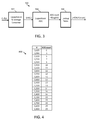
- Fig. 3 shows another illustrative embodiment of a fingerprint sensing system 300.
- the system 300 comprises a capacitance-to-voltage converter 302, a logarithmic analog-to-digital converter 304 operatively coupled to the capacitance-to-voltage converter 302, and a lookup table 306 operatively coupled to the logarithmic analog-to-digital converter 304.
- the capacitance-to-voltage converter 302 converts a measured capacitance, which may be regarded as a function of a valley depth z, into a voltage, which may thus be regarded as a function of the measured capacitance.
- the logarithmic analog-to-digital converter 304 converts the voltage into a digital signal, in particular a value ADC count .
- the lookup table 306 takes the value ADC count as input and outputs a value z representing the measured valley depth.
- the system 300 comprises a post-conversion unit configured to produce, for a given value ADC count of the digital signal, an associated precomputed output value z.
- the post-conversion unit includes a lookup table 306 comprising a plurality of digital signal values and associated precomputed output values.
- the look-up table 306 is configurable by a host processor. In this way, the fingerprint sensing system 300 may easily be tuned.
- the passivation capacitance C passivation may be determined by the passivation thickness and its k-factor, wherein the k-factor is the material-specific dielectric constant. This capacitance is relatively large.
- the coating capacitance C coating may be determined by the coating thickness and its k-factor, resulting in a capacitance that has the same order of magnitude as the capacitance C z .
- V cap b * c / a * b + z
- a logarithm with a base of 2 1/x in the log(2) domain may be expressed as: ⁇ ld V cap / c , wherein ld represents the logarithm with base 2 ( logarithmus dualis ).
- the value of 1/c may be pre-calculated in order to substitute division by multiplication.
- An ADC with logarithmic conversion function may now be applied which may combine sampling and logarithmization in one step.
- Fig. 5 shows an illustrative embodiment of a linearization function implementation 500.
- the implementation comprises the aforementioned barrel-shift left operation SHL.
- Fig. 6 shows an output of an analog-to-digital converter as a function 600 of the real valley depth z.
- the x-axis represents the sensor plate gap in ⁇ m
- the y-axis shows the obtained measurement value ADC count , in this example with an applied attenuation factor that may provide an option to store the value in a 4-bit variable.
- 4-bit variables may enable packing two 4-bit variables into one data byte which may reduce bandwidth requirements for data transfer to a host processor. Since the data transfer to the host processor is often a bottleneck in image capture time, this may also increase the image capture rate. Due to cut-off effects resulting from integer conversion in the logarithmic domain deviations from an ideal conversion may occur in the sensor plate distance readings. However, due to the nature of fingerprint image processing the impact of these deviations is neglectable.
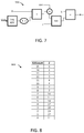
- Fig. 7 shows another illustrative embodiment of a linearization function implementation 700.
- a linearization function implementation in which an adjustment factor is used which may be useful if the logarithmic conversion has a base different from two. That is to say, in some embodiments logarithmization may be implemented on a base that is different from 2, which may give a finer sampling resolution. Since de-logarithmization in the binary domain may easily be achieved for a logarithm base of 2, the value provided by the logarithmic ADC may be adjusted to a base of 2 by applying an adjustment factor corr.
- the adjustment factor may be calculated as follows:
- the adjustment factor corr is a constant that may be pre-calculated. It is useful to choose the logarithm base such that corr may result in a value that supports easy integer calculations.
- fully pre-calculated terms "[1 SHL(A - ADCcount * corr)] - b" may be stored in the look-up table 306, which in that case may hold for every discrete ADC count one z-term that directly translates ADC count into the measured valley depth z. This approach simplifies the calculation of z:
- Fig. 8 shows an illustrative embodiment of a lookup table 800.
- the look-up table 800 comprises for every discrete ADC count one z-term that directly translates ADC count into the measured valley depth z. In this way, the calculation of the measured valley depth z is simplified.
- Fig. 9 shows an example of how the real valley depth differs from a measured valley depth.
- it shows on the x-axis the real valley depth in ⁇ m, and on the y-axis the measured valley depth in ⁇ m.
- Reference line 900 shows an exact correspondence between the real valley depth and the measured valley depth. That is to say, reference line 900 shows the measurement result of an ideal fingerprint sensing system.
- Line 902 shows the measured valley depth as a function of the real valley depth.
- the output is illustrated of a fingerprint sensing system implemented in accordance with the above-described embodiments. It can be seen that the output represented by line 902 is fairly linear. Thus, the output is relatively accurate while the need for computational resources is not too high. Furthermore, noise clipping has been applied for valley depths greater than 26 ⁇ m.
- Fig. 10 shows another example of how the real valley depth differs from a measured valley depth. Again, it shows on the x-axis the real valley depth in ⁇ m, and on the y-axis the measured valley depth in ⁇ m.
- Reference line 1000 shows an exact correspondence between the real valley depth and the measured valley depth. That is to say, reference line 1000 shows the measurement result of an ideal fingerprint sensing system.
- Line 1002 shows the measured valley depth as a function of the real valley depth.
- line 1002 represents the output of a fingerprint sensing system comprising a linear ADC. It can be seen that, in comparison to the output illustrated in Fig. 9 , the output represented by line 1002 deviates significantly from the ideal output represented by reference line 1000. In particular for large valley depths the output is not sufficiently accurate.
- the look-up table as shown in Fig. 8 may be stored in a volatile memory, such as a RAM, which enables installation of table data by a host processor. This approach may enable the host processor to adjust the look-up table according to application needs in real-time.
- a fast Fourier transformation is applied to the samples provided by the look-up table.
- the look-up table may be configured to provide output values that are powers of 2 which may simplify a consecutive FFT calculation because many coefficients may become 0. This may speed up the FFT calculation and hence save calculation resources and may reduce the power consumption.
- a logarithmic pipelined ADC may be utilized. The logarithmic conversion principle may simplify the ADC design because fewer subtractions are required compared to a linear ADC.
- a flash ADC may be utilized. In this configuration 15 comparators may be required for a 16 step logarithmic ADC.
- a switched capacitor voltage divider may be utilized to provide the reference voltage levels by charge division, thus making sure that non-integer factors are applied such that a monotonous conversion characteristic is achieved.
- hi-k material with a k-factor of 8 to 18 and above is used for the coating material in order to compensate for the coating thickness, thereby increasing the sensitivity of the sensor.
- Fig. 11 shows another illustrative embodiment of a conversion function 1100 of an analog-to-digital converter.
- the ADC may be an ADC with reciprocal conversion characteristic, followed by post-conversion unit including a lookup table for deriving z from the ADC reading ADC count .
- the reciprocal conversion characteristic may provide minimal quantization noise and may provide a direct linear representation of the sensor plate distance.
- the quantization noise is now solely determined by the variation of the comparator reference levels in the ADC. Reference level adjustment by trimming during manufacturing may be applied to minimize this sort of noise.
- the reciprocal ADC conversion characteristic may be best implemented by a flash ADC with fixed reference levels for the individual quantization levels.
- An example of an ADC conversion characteristic with a conversion range of 2V is shown in Fig. 11 . It is a characteristic of reciprocal ADCs that the comparator resolution may increase towards lower input voltages. This also means that the comparator gain may be increased towards lower input voltages, so that power may be saved for larger input voltages.
- the conversion function is made adjustable during production by means of, for example, laser trimming, flash programming or other suitable methods.
- the comparator gain is adapted to the input voltage level by adapting its bias/supply current.
- the non-linear conversion results may be provided to a micro-processing unit for applying the linearization calculation steps. This may be useful if a coarse scan at reduced quantization is required for time and power saving purposes.
- the systems and methods described herein may at least partly be embodied by a computer program or a plurality of computer programs, which may exist in a variety of forms both active and inactive in a single computer system or across multiple computer systems.
- they may exist as software program(s) comprised of program instructions in source code, object code, executable code or other formats for performing some of the steps.
- Any of the above may be embodied on a computer-readable medium, which may include storage devices and signals, in compressed or uncompressed form.
- the term “mobile device” refers to any type of portable electronic device, including a cellular telephone, a Personal Digital Assistant (PDA), smartphone, tablet etc.
- the term “computer” refers to any electronic device comprising a processor, such as a general-purpose central processing unit (CPU), a specific-purpose processor or a microcontroller.
- CPU central processing unit
- a computer is capable of receiving data (an input), of performing a sequence of predetermined operations thereupon, and of producing thereby a result in the form of information or signals (an output).
- the term “computer” will mean either a processor in particular or more generally a processor in association with an assemblage of interrelated elements contained within a single case or housing.
- processor or “processing unit” refers to a data processing circuit that may be a microprocessor, a co-processor, a microcontroller, a microcomputer, a central processing unit, a field programmable gate array (FPGA), a programmable logic circuit, and/or any circuit that manipulates signals (analog or digital) based on operational instructions that are stored in a memory.
- memory refers to a storage circuit or multiple storage circuits such as read-only memory, random access memory, volatile memory, non-volatile memory, static memory, dynamic memory, Flash memory, cache memory, and/or any circuit that stores digital information.
- a "computer-readable medium” or “storage medium” may be any means that can contain, store, communicate, propagate, or transport a computer program for use by or in connection with the instruction execution system, apparatus, or device.
- the computer-readable medium may be, for example but not limited to, an electronic, magnetic, optical, electromagnetic, infrared, or semiconductor system, apparatus, device, or propagation medium.
- the computer-readable medium may include the following: an electrical connection having one or more wires, a portable computer diskette, a random access memory (RAM), a read-only memory (ROM), an erasable programmable read-only memory (EPROM or Flash memory), an optical fiber, a portable compact disc read-only memory (CDROM), a digital versatile disc (DVD), a Blu-ray disc (BD), and a memory card.
- RAM random access memory
- ROM read-only memory
- EPROM or Flash memory erasable programmable read-only memory
- CDROM compact disc read-only memory
- DVD digital versatile disc
- BD Blu-ray disc
Landscapes
- Engineering & Computer Science (AREA)
- Human Computer Interaction (AREA)
- Physics & Mathematics (AREA)
- General Physics & Mathematics (AREA)
- Multimedia (AREA)
- Theoretical Computer Science (AREA)
- Image Input (AREA)
- Measurement Of Length, Angles, Or The Like Using Electric Or Magnetic Means (AREA)
- Measurement Of The Respiration, Hearing Ability, Form, And Blood Characteristics Of Living Organisms (AREA)
Abstract
Description
- The present disclosure relates to a fingerprint sensing system. Furthermore, the present disclosure relates to a corresponding fingerprint sensing method and to a corresponding computer program product.
- Today, many electronic devices and systems require a form of user authentication. For example, in a payment system, a smart card may be used to initiate a payment and to authenticate a user. In addition to conventional user authentication via a personal identification number (PIN), a smart card may also include a fingerprint sensor for capturing the user's fingerprint. In that case, the captured fingerprint may be used to ascertain that the smart card is presented to a terminal by its rightful owner, for example. However, capturing a user's fingerprint with sufficient accuracy may be difficult.
- According to a first aspect of the present disclosure, a fingerprint sensing system is provided, comprising: a sensing unit configured to measure a physical property of a sensing cell and to produce a voltage in dependence on said physical property; and an analog-to-digital converter configured to convert said voltage into a digital signal, wherein said analog-to-digital converter implements a non-linear conversion function.
- In one or more embodiments, the analog-to-digital converter implements a logarithmic conversion function.
- In one or more embodiments, the logarithmic conversion function has a base of two.
- In one or more embodiments, the system further comprises a post-conversion unit configured to produce, for a given value of the digital signal, an associated precomputed output value.
- In one or more embodiments, the post-conversion unit is configured to use, for producing said precomputed output value, a look-up table comprising a plurality of digital signal values and associated precomputed output values.
- In one or more embodiments, the look-up table is configurable by a host processor.
- In one or more embodiments, the system further comprises a transformation unit configured to perform a fast Fourier transformation on output values produced by the post-conversion unit.
- In one or more embodiments, the physical property represents the distance between a surface of the sensing cell and the surface of a finger.
- In one or more embodiments, the physical property is an electrical capacitance.
- In one or more embodiments, the analog-to-digital converter is a logarithmic pipelined analog-to-digital converter.
- In one or more embodiments, the analog-to-digital converter is a flash analog-to-digital converter.
- In one or more embodiments, the analog-to-digital converter has a reciprocal conversion characteristic.
- In one or more embodiments, a smart card comprises a system of the kind set forth.
- According to a second aspect of the present disclosure, a fingerprint sensing method is conceived, comprising: a sensing unit measures a physical property of a sensing cell and produces a voltage in dependence on said physical property; and an analog-to-digital converter that implements a non-linear conversion function converts said voltage into a digital signal.
- According to a third aspect of the present disclosure, a computer program product is provided, the computer program product comprising non-transient instructions which, when executed by a processing unit, cause said processing unit to carry out or control a method of the kind set forth.
- Embodiments will be described in more detail with reference to the appended drawings, in which:
-
Fig. 1 shows an example of a sensing cell; -
Fig. 2 shows an illustrative embodiment of a fingerprint sensing system; -
Fig. 3 shows another illustrative embodiment of a fingerprint sensing system; -
Fig. 4 shows an illustrative embodiment of a conversion function of an analog-to-digital converter; -
Fig. 5 shows an illustrative embodiment of a linearization function implementation; -
Fig. 6 shows an output of an analog-to-digital converter as a function of the valley depth; -
Fig. 7 shows another illustrative embodiment of a linearization function implementation; -
Fig. 8 shows an illustrative embodiment of a lookup table; -
Fig. 9 shows an example of how the real valley depth differs from a measured valley depth; -
Fig. 10 shows another example of how the real valley depth differs from a measured valley depth; -
Fig. 11 shows another illustrative embodiment of a conversion function of an analog-to-digital converter. -
Fig. 1 shows an example of asensing cell 100. Thesensing cell 100 may form part of a fingerprint sensing system, which may for example be embedded in a smart card. Such a fingerprint sensing system may comprise a plurality of sensing cells, which may be arranged in the form of a matrix, for example. Each sensing cell may have a physical property that may change in response to the proximity of an external object, for instance a human finger. In this example, thesensing cell 100 comprises asensor plate 102, apassivation layer 104 and acoating 106. In this case, the physical property of the sensing cell is an electrical capacitance that may change in dependence on the distance between the upper surface of thesensing cell 100 and the surface of ahuman finger 108. - In particular, the
sensor plate 102 is covered by apassivation layer 104 that may be made from silicon nitride. A protective scratch and wear protection in the form of acoating 106 is applied on thepassivation layer 104. While thepassivation layer 104 may have a thickness in the order of 1 µm to 3 µm, the typical thickness of thecoating 106 is in the order of 25 µm to 50 µm. The valley depth z, i.e. the distance between the surface of thesensing cell 100 and the surface of thefinger 108, is usually in the order of 25 µm. Thepassivation layer 104, thecoating 106 and the valley may have different dielectric constants, named k-factors. The k-factor of thepassivation layer 104 is in the order of 2-4, the k-factor of thecoating 106 is in the order of 2-4 and the k-factor of the valley is the k-factor of air, which is 1. The total capacitance of the sensing cell, which may be measured by a sensing unit (not shown), may be expressed as Cmeas:
- The capacitance Cmeas is normally a non-linear function of the valley depth z, and vice versa, with the characteristic of a reciprocal function. A fingerprint sensing system may use a measured capacitance Cmeas for determining the valley depth z between a particular cell and the finger. Accordingly, if measurements are taken from a plurality of sensing cells, a fingerprint's topology may be determined. Fingerprint sensors often utilize high-resolution linear analog-to-digital converters (ADCs) to generate a digital representation of the capacitance Cmeas. High-resolution ADCs consume processing time, die area and power. Furthermore, fingerprint sensors often apply low-pass-filtering in combination with high resolution sampling (e.g. 508dpi) to obtain images having sufficient quality for good fingerprint detection. One of the critical noise sources that degrades the signal-to-noise ratio is the quantization noise. The inventor has realized that, due to the nature of the measured capacitance Cmeas, a linear ADC may not represent an optimal solution when low quantization noise is required. If the quantization noise can be reduced, even fingerprint sensors with a lower resolution (e.g. 250dpi) may be used to provide a good three-dimensional resolution.
- Typically, for small valley depths, the resolution is high in the sense that different valley depths yield capacitance values which can be sufficiently distinguished from each other, while for larger valley depths, the resolution is low in the sense that different valley depths yield capacitance values which cannot be distinguished well from each other. Therefore, a linearization of the measurement result may be required. However, a linearization of the measurement result may require time-consuming post-processing operations which consume valuable computational resources in a fingerprint authentication system. Furthermore, in resource-constrained systems, it may even be impossible to implement such a linearization. Therefore, it may be desirable to reduce the linearization effort in order to reduce the required computational resources and furthermore to reduce the integral power consumption of a fingerprint sensor and authentication system. Furthermore, it may be desirable to reduce the effort required for analog-to-digital conversion in terms of quantization, power, speed and die area consumption.
- Therefore, in accordance with the present disclosure, a fingerprint sensing system is provided, comprising a sensing unit configured to measure a physical property of a sensing cell and to produce a voltage in dependence on said physical property, and an analog-to-digital converter configured to convert said voltage into a digital signal, wherein said analog-to-digital converter implements a non-linear conversion function. Furthermore, a corresponding fingerprint sensing method is conceived. In particular, the inventor has found that the use of an ADC having a non-linear conversion characteristic (i.e., implementing a non-linear conversion function) may reduce the amount of required computations, and thus the need for computational resources, while still enabling a linearization of the measurement result. In particular, the inventor has found that an ADC implementing a logarithmic conversion function may further reduce the amount of required computations while still enabling a linearization of the measurement result. In a practical and efficient implementation, the logarithmic conversion function has a base of two.
-
Fig. 2 shows an illustrative embodiment of afingerprint sensing system 200. Thefingerprint sensing system 200 comprises asensing unit 202 and a non-linear analog-to-digital converter 204 which are operatively coupled to each other. In operation, thesensing unit 202 measures a physical property, such as an electrical capacitance, from a sensing cell (not shown) and produces a voltage in dependence on the measured property. Furthermore, the non-linear analog-to-digital converter 204 converts the voltage into a digital signal. -
Fig. 3 shows another illustrative embodiment of afingerprint sensing system 300. In this example, thesystem 300 comprises a capacitance-to-voltage converter 302, a logarithmic analog-to-digital converter 304 operatively coupled to the capacitance-to-voltage converter 302, and a lookup table 306 operatively coupled to the logarithmic analog-to-digital converter 304. In operation, the capacitance-to-voltage converter 302 converts a measured capacitance, which may be regarded as a function of a valley depth z, into a voltage, which may thus be regarded as a function of the measured capacitance. The logarithmic analog-to-digital converter 304 converts the voltage into a digital signal, in particular a value ADCcount. The lookup table 306 takes the value ADCcount as input and outputs a value z representing the measured valley depth. - Thus, in this embodiment, the
system 300 comprises a post-conversion unit configured to produce, for a given value ADCcount of the digital signal, an associated precomputed output value z. In particular, the post-conversion unit includes a lookup table 306 comprising a plurality of digital signal values and associated precomputed output values. In this way, calculation efforts may be further reduced and therefore less computational resources may be required. The inventor has found that the use of alogarithmic ADC 304 in combination with a lookup table 306 enables a particularly efficient implementation of the aforementioned linearization. Furthermore, in one or more embodiments, the look-up table 306 is configurable by a host processor. In this way, thefingerprint sensing system 300 may easily be tuned. - A more detailed example embodiment may be described as follows. As mentioned above, the measured capacitance comprises the following components:

- Since both Cpassivation and Ccoating are defined during manufacturing of the fingerprint sensor these capacitances may be assumed as being constant within one fingerprint image scan, having the capacitance Cconst, expressed by its inverse value a as:


- The voltage Vcap provided by the capacitance-to-
voltage converter 302 may be regarded as linearly dependent on Cmeas with c being the conversion factor:

- Cmeas may now be expressed as a function of z:


- The measured valley depth z may now be obtained as follows:


- In accordance with the present disclosure the term (c Vcap) may be evaluated in the logarithmic domain:

- In case a logarithm with a base of 2 is used 1/x in the log(2) domain may be expressed as:

- This yields for z:

- In a practical and efficient implementation, the value of 1/c may be pre-calculated in order to substitute division by multiplication. An ADC with logarithmic conversion function may now be applied which may combine sampling and logarithmization in one step.
- In some embodiments the logarithmization may be implemented as:

-
Fig. 4 shows an illustrative embodiment of anon-linear conversion function 400 of an analog-to-digital converter. That is to say, in the particular example described here, the ADC conversion function may be defined by the values shown in the table depicted inFig. 4 . It is noted that ld (b) is a constant and maybe set to ld (b) = A. - This may yield:

- This power of 2 exponentiation may be realized by a shift-left operation:

-
Fig. 5 shows an illustrative embodiment of alinearization function implementation 500. The implementation comprises the aforementioned barrel-shift left operation SHL. -
Fig. 6 shows an output of an analog-to-digital converter as afunction 600 of the real valley depth z. In particular, it shows an example of the conversion of the sensor plate gap (i.e., the real valley depth) to its related digital value (i.e., the value ADCcount). The x-axis represents the sensor plate gap in µm, the y-axis shows the obtained measurement value ADCcount, in this example with an applied attenuation factor that may provide an option to store the value in a 4-bit variable. Using 4-bit variables may enable packing two 4-bit variables into one data byte which may reduce bandwidth requirements for data transfer to a host processor. Since the data transfer to the host processor is often a bottleneck in image capture time, this may also increase the image capture rate. Due to cut-off effects resulting from integer conversion in the logarithmic domain deviations from an ideal conversion may occur in the sensor plate distance readings. However, due to the nature of fingerprint image processing the impact of these deviations is neglectable. -
Fig. 7 shows another illustrative embodiment of alinearization function implementation 700. In particular, it shows a linearization function implementation in which an adjustment factor is used, which may be useful if the logarithmic conversion has a base different from two. That is to say, in some embodiments logarithmization may be implemented on a base that is different from 2, which may give a finer sampling resolution. Since de-logarithmization in the binary domain may easily be achieved for a logarithm base of 2, the value provided by the logarithmic ADC may be adjusted to a base of 2 by applying an adjustment factor corr. The adjustment factor may be calculated as follows: - log(x)base = ld(x) / ld(base),
wherein ld() is the logarithm withbase 2. Then:- ld(x) = ld(x)base * corr
- corr = ld(base)
- The adjustment factor corr is a constant that may be pre-calculated. It is useful to choose the logarithm base such that corr may result in a value that supports easy integer calculations. The valley depth z may now be obtained as follows:

- The resulting conversion steps are illustrated in Fig.. In some embodiments pre-calculated products "ADCcount * corr" may be stored in a table that holds for every discrete ADCcount one product term. This approach avoids implementation of a hardware multiplier and simplifies the multiplication to a table-lookup which is fast and does not consume resources. For a 16-
step logarithmization 15 memory locations are required (an ADC value of 0 will provide 0):
- Referring back to
Fig. 3 , in some embodiments fully pre-calculated terms "[1 SHL(A - ADCcount * corr)] - b" may be stored in the look-up table 306, which in that case may hold for every discrete ADCcount one z-term that directly translates ADCcount into the measured valley depth z. This approach simplifies the calculation of z: - z = lookup(ADCcount)
- In this way, an efficient and fast way of obtaining the measured valley depth z from the logarithmic ADC reading is provided, without a need for a hardware multiplier or a barrel shifter and furthermore utilizing the fact that z is solely a function of ADCcount. This approach is feasible because the discrete output of the logarithmic ADC has a limited definition space of [0, 1 ... samples]. For 32 discrete output values, for example, 31 terms need to be stored. If every term is represented by a 4-bit value two of these values may be packed into one byte, thereby reducing the required table to 16 bytes in the given example.
-
Fig. 8 shows an illustrative embodiment of a lookup table 800. As described with reference toFig. 7 above, the look-up table 800 comprises for every discrete ADCcount one z-term that directly translates ADCcount into the measured valley depth z. In this way, the calculation of the measured valley depth z is simplified. -
Fig. 9 shows an example of how the real valley depth differs from a measured valley depth. In particular, it shows on the x-axis the real valley depth in µm, and on the y-axis the measured valley depth in µm.Reference line 900 shows an exact correspondence between the real valley depth and the measured valley depth. That is to say,reference line 900 shows the measurement result of an ideal fingerprint sensing system.Line 902 shows the measured valley depth as a function of the real valley depth. Here, the output is illustrated of a fingerprint sensing system implemented in accordance with the above-described embodiments. It can be seen that the output represented byline 902 is fairly linear. Thus, the output is relatively accurate while the need for computational resources is not too high. Furthermore, noise clipping has been applied for valley depths greater than 26 µm. -
Fig. 10 shows another example of how the real valley depth differs from a measured valley depth. Again, it shows on the x-axis the real valley depth in µm, and on the y-axis the measured valley depth in µm.Reference line 1000 shows an exact correspondence between the real valley depth and the measured valley depth. That is to say,reference line 1000 shows the measurement result of an ideal fingerprint sensing system.Line 1002 shows the measured valley depth as a function of the real valley depth. In this example,line 1002 represents the output of a fingerprint sensing system comprising a linear ADC. It can be seen that, in comparison to the output illustrated inFig. 9 , the output represented byline 1002 deviates significantly from the ideal output represented byreference line 1000. In particular for large valley depths the output is not sufficiently accurate. - In some embodiments the look-up table as shown in
Fig. 8 may be stored in a volatile memory, such as a RAM, which enables installation of table data by a host processor. This approach may enable the host processor to adjust the look-up table according to application needs in real-time. Furthermore, in some embodiments the logarithm base may be calculated in dependence on the signal-to-noise ratio of the capacitance-to-voltage convertor 302 of the fingerprint sensing cell. In particular, for a given input voltage range Vrange and an S/N-ratio the noise level may be calculated as follows:
- The logarithm base may be calculated from the S/N ratio and the number of samples as follows:

- As an example, for a conversion voltage range of 2V, an S/N of 100 (40dB) and 16 steps the logarithm base may be:

- In some embodiments a fast Fourier transformation (FFT) is applied to the samples provided by the look-up table. The look-up table may be configured to provide output values that are powers of 2 which may simplify a consecutive FFT calculation because many coefficients may become 0. This may speed up the FFT calculation and hence save calculation resources and may reduce the power consumption. In some embodiments a logarithmic pipelined ADC may be utilized. The logarithmic conversion principle may simplify the ADC design because fewer subtractions are required compared to a linear ADC. In some embodiments a flash ADC may be utilized. In this
configuration 15 comparators may be required for a 16 step logarithmic ADC. A switched capacitor voltage divider may be utilized to provide the reference voltage levels by charge division, thus making sure that non-integer factors are applied such that a monotonous conversion characteristic is achieved. In some embodiments hi-k material with a k-factor of 8 to 18 and above is used for the coating material in order to compensate for the coating thickness, thereby increasing the sensitivity of the sensor. -
Fig. 11 shows another illustrative embodiment of aconversion function 1100 of an analog-to-digital converter. In particular, it shows aconversion function 1100 of an ADC with a reciprocal conversion characteristic. In some embodiments the ADC may be an ADC with reciprocal conversion characteristic, followed by post-conversion unit including a lookup table for deriving z from the ADC reading ADCcount. The reciprocal conversion characteristic may provide minimal quantization noise and may provide a direct linear representation of the sensor plate distance. The quantization noise is now solely determined by the variation of the comparator reference levels in the ADC. Reference level adjustment by trimming during manufacturing may be applied to minimize this sort of noise. The conversion characteristic of the ADC may be defined as:
- With a=16 for 16 quantization levels this may result in an accurate output. The reciprocal ADC conversion characteristic may be best implemented by a flash ADC with fixed reference levels for the individual quantization levels. An example of an ADC conversion characteristic with a conversion range of 2V is shown in
Fig. 11 . It is a characteristic of reciprocal ADCs that the comparator resolution may increase towards lower input voltages. This also means that the comparator gain may be increased towards lower input voltages, so that power may be saved for larger input voltages. - In some embodiments the conversion function is made adjustable during production by means of, for example, laser trimming, flash programming or other suitable methods. In some embodiments the comparator gain is adapted to the input voltage level by adapting its bias/supply current. Furthermore, in some embodiments the non-linear conversion results may be provided to a micro-processing unit for applying the linearization calculation steps. This may be useful if a coarse scan at reduced quantization is required for time and power saving purposes.
- The systems and methods described herein may at least partly be embodied by a computer program or a plurality of computer programs, which may exist in a variety of forms both active and inactive in a single computer system or across multiple computer systems. For example, they may exist as software program(s) comprised of program instructions in source code, object code, executable code or other formats for performing some of the steps. Any of the above may be embodied on a computer-readable medium, which may include storage devices and signals, in compressed or uncompressed form.
- As used herein, the term "mobile device" refers to any type of portable electronic device, including a cellular telephone, a Personal Digital Assistant (PDA), smartphone, tablet etc. Furthermore, the term "computer" refers to any electronic device comprising a processor, such as a general-purpose central processing unit (CPU), a specific-purpose processor or a microcontroller. A computer is capable of receiving data (an input), of performing a sequence of predetermined operations thereupon, and of producing thereby a result in the form of information or signals (an output). Depending on the context, the term "computer" will mean either a processor in particular or more generally a processor in association with an assemblage of interrelated elements contained within a single case or housing.
- The term "processor" or "processing unit" refers to a data processing circuit that may be a microprocessor, a co-processor, a microcontroller, a microcomputer, a central processing unit, a field programmable gate array (FPGA), a programmable logic circuit, and/or any circuit that manipulates signals (analog or digital) based on operational instructions that are stored in a memory. The term "memory" refers to a storage circuit or multiple storage circuits such as read-only memory, random access memory, volatile memory, non-volatile memory, static memory, dynamic memory, Flash memory, cache memory, and/or any circuit that stores digital information.
- As used herein, a "computer-readable medium" or "storage medium" may be any means that can contain, store, communicate, propagate, or transport a computer program for use by or in connection with the instruction execution system, apparatus, or device. The computer-readable medium may be, for example but not limited to, an electronic, magnetic, optical, electromagnetic, infrared, or semiconductor system, apparatus, device, or propagation medium. More specific examples (non-exhaustive list) of the computer-readable medium may include the following: an electrical connection having one or more wires, a portable computer diskette, a random access memory (RAM), a read-only memory (ROM), an erasable programmable read-only memory (EPROM or Flash memory), an optical fiber, a portable compact disc read-only memory (CDROM), a digital versatile disc (DVD), a Blu-ray disc (BD), and a memory card.
- It is noted that the embodiments above have been described with reference to different subject-matters. In particular, some embodiments may have been described with reference to method-type claims whereas other embodiments may have been described with reference to apparatus-type claims. However, a person skilled in the art will gather from the above that, unless otherwise indicated, in addition to any combination of features belonging to one type of subject-matter also any combination of features relating to different subject-matters, in particular a combination of features of the method-type claims and features of the apparatus-type claims, is considered to be disclosed with this document.
- Furthermore, it is noted that the drawings are schematic. In different drawings, similar or identical elements are provided with the same reference signs. Furthermore, it is noted that in an effort to provide a concise description of the illustrative embodiments, implementation details which fall into the customary practice of the skilled person may not have been described. It should be appreciated that in the development of any such implementation, as in any engineering or design project, numerous implementation-specific decisions must be made in order to achieve the developers' specific goals, such as compliance with system-related and business-related constraints, which may vary from one implementation to another. Moreover, it should be appreciated that such a development effort might be complex and time consuming, but would nevertheless be a routine undertaking of design, fabrication, and manufacture for those of ordinary skill.
- Finally, it is noted that the skilled person will be able to design many alternative embodiments without departing from the scope of the appended claims. In the claims, any reference sign placed between parentheses shall not be construed as limiting the claim. The word "comprise(s)" or "comprising" does not exclude the presence of elements or steps other than those listed in a claim. The word "a" or "an" preceding an element does not exclude the presence of a plurality of such elements. Measures recited in the claims may be implemented by means of hardware comprising several distinct elements and/or by means of a suitably programmed processor. In a device claim enumerating several means, several of these means may be embodied by one and the same item of hardware. The mere fact that certain measures are recited in mutually different dependent claims does not indicate that a combination of these measures cannot be used to advantage.
-
- 100
- sensing cell
- 102
- sensor plate
- 104
- passivation layer
- 106
- coating
- 108
- finger
- 200
- fingerprint sensing system
- 202
- sensing unit
- 204
- non-linear analog-to-digital converter
- 300
- fingerprint sensing system
- 302
- capacitance-to-voltage converter
- 304
- logarithmic analog-to-digital converter
- 306
- lookup table
- 400
- conversion function of analog-to-digital converter
- 500
- implementation of linearization function
- 600
- ADC output as function of valley depth
- 700
- implementation of linearization function
- 800
- lookup table
- 900
- reference line
- 902
- measured valley depth as function of real valley depth
- 1000
- reference line
- 1002
- measured valley depth as function of real valley depth
- 1100
- conversion function of analog-to-digital converter
Claims (15)
- A fingerprint sensing system, comprising:a sensing unit configured to measure a physical property of a sensing cell and to produce a voltage in dependence on said physical property;an analog-to-digital converter configured to convert said voltage into a digital signal, wherein said analog-to-digital converter implements a non-linear conversion function.
- The system of claim 1, wherein the analog-to-digital converter implements a logarithmic conversion function.
- The system of claim 2, wherein the logarithmic conversion function has a base of two.
- The system of any preceding claim, further comprising a post-conversion unit configured to produce, for a given value of the digital signal, an associated precomputed output value.
- The system of claim 4, wherein the post-conversion unit is configured to use, for producing said precomputed output value, a look-up table comprising a plurality of digital signal values and associated precomputed output values.
- The system of claim 5, wherein the look-up table is configurable by a host processor.
- The system of any one of claims 4 to 6, further comprising a transformation unit configured to perform a fast Fourier transformation on output values produced by the post-conversion unit.
- The system of any preceding claim, wherein the physical property represents the distance between a surface of the sensing cell and the surface of a finger.
- The system of any preceding claim, wherein the physical property is an electrical capacitance.
- The system of any preceding claim, wherein the analog-to-digital converter is a logarithmic pipelined analog-to-digital converter.
- The system of any preceding claim, wherein the analog-to-digital converter is a flash analog-to-digital converter.
- The system of any preceding claim, wherein the analog-to-digital converter has a reciprocal conversion characteristic.
- A smart card comprising the fingerprint sensing system of any preceding claim.
- A fingerprint sensing method, comprising:a sensing unit measures a physical property of a sensing cell and produces a voltage in dependence on said physical property;an analog-to-digital converter that implements a non-linear conversion function converts said voltage into a digital signal.
- A computer program product comprising non-transient instructions which, when executed by a processing unit, cause said processing unit to carry out or control the method of claim 14.
Priority Applications (3)
| Application Number | Priority Date | Filing Date | Title |
|---|---|---|---|
| EP16177943.4A EP3267358B1 (en) | 2016-07-05 | 2016-07-05 | Fingerprint sensing system and method |
| CN201710499673.XA CN107578242B (en) | 2016-07-05 | 2017-06-27 | Fingerprint sensing system and method |
| US15/642,272 US10482306B2 (en) | 2016-07-05 | 2017-07-05 | Fingerprint sensing system and method |
Applications Claiming Priority (1)
| Application Number | Priority Date | Filing Date | Title |
|---|---|---|---|
| EP16177943.4A EP3267358B1 (en) | 2016-07-05 | 2016-07-05 | Fingerprint sensing system and method |
Publications (2)
| Publication Number | Publication Date |
|---|---|
| EP3267358A1 true EP3267358A1 (en) | 2018-01-10 |
| EP3267358B1 EP3267358B1 (en) | 2021-10-13 |
Family
ID=56368862
Family Applications (1)
| Application Number | Title | Priority Date | Filing Date |
|---|---|---|---|
| EP16177943.4A Active EP3267358B1 (en) | 2016-07-05 | 2016-07-05 | Fingerprint sensing system and method |
Country Status (3)
| Country | Link |
|---|---|
| US (1) | US10482306B2 (en) |
| EP (1) | EP3267358B1 (en) |
| CN (1) | CN107578242B (en) |
Families Citing this family (2)
| Publication number | Priority date | Publication date | Assignee | Title |
|---|---|---|---|---|
| EP3232369B1 (en) | 2016-04-15 | 2021-06-16 | Nxp B.V. | Fingerprint authentication system and method |
| TWM608543U (en) * | 2020-03-02 | 2021-03-01 | 神盾股份有限公司 | Integrated spectrum sensing device for real-finger judgement |
Citations (1)
| Publication number | Priority date | Publication date | Assignee | Title |
|---|---|---|---|---|
| EP2403146A1 (en) * | 2010-06-29 | 2012-01-04 | University of Limerick | Low power analog to digital converter |
Family Cites Families (9)
| Publication number | Priority date | Publication date | Assignee | Title |
|---|---|---|---|---|
| TWI397862B (en) * | 2007-06-22 | 2013-06-01 | Mstar Semiconductor Inc | Fingerprint sensor |
| US9195877B2 (en) * | 2011-12-23 | 2015-11-24 | Synaptics Incorporated | Methods and devices for capacitive image sensing |
| US9361064B2 (en) * | 2013-09-10 | 2016-06-07 | Intel Corporation | Methods and systems to compensate for non-linearity of a stochastic system |
| CN103810479B (en) * | 2014-02-28 | 2019-04-05 | 成都费恩格尔微电子技术有限公司 | Fingerprint acquisition system and fingerprint information acquisition method |
| CN103778420B (en) * | 2014-02-28 | 2018-11-09 | 成都费恩格尔微电子技术有限公司 | fingerprint detection system with automatic gain control and automatic gain control method thereof |
| CN105447439B (en) * | 2015-02-13 | 2017-05-03 | 比亚迪股份有限公司 | Fingerprint detection circuit and electronic device |
| KR20160138917A (en) * | 2015-05-26 | 2016-12-06 | 크루셜텍 (주) | Smart card comprising fingerprint detecting device and method for driving the same |
| CN105389544B (en) * | 2015-10-21 | 2018-04-17 | 深圳市汇顶科技股份有限公司 | Output conversion circuit and fingerprint recognition system |
| CN205302320U (en) * | 2015-12-08 | 2016-06-08 | 北京集创北方科技有限公司 | Fingerprint identification device |
-
2016
- 2016-07-05 EP EP16177943.4A patent/EP3267358B1/en active Active
-
2017
- 2017-06-27 CN CN201710499673.XA patent/CN107578242B/en active Active
- 2017-07-05 US US15/642,272 patent/US10482306B2/en active Active
Patent Citations (1)
| Publication number | Priority date | Publication date | Assignee | Title |
|---|---|---|---|---|
| EP2403146A1 (en) * | 2010-06-29 | 2012-01-04 | University of Limerick | Low power analog to digital converter |
Non-Patent Citations (7)
| Title |
|---|
| "CMOS Telecom Data Converters", 1 January 2003, SPRINGER, article JORGE GUILHERME ET AL: "LOGARITHMIC A NALOGUE-TO-DIGITAL CONVERTERS Logarithmic Analogue-to-Digital Converters", pages: 241 - 275, XP055330319 * |
| "Integrated Smart Sensors", 31 December 1998, SPRINGER, ISBN: 978-1-4757-2890-3, article GERT VAN DER HORN ET AL: "Linearization based on look-up table", pages: 60 - 63, XP055361539 * |
| FRANCESCONI F ET AL: "A LOW POWER LOGARITHMIC A/D CONVERTER", 1996 IEEE INTERNATIONAL SYMPOSIUM ON CIRCUITS AND SYSTEMS (ISCAS). CIRCUITS AND SYSTEMS CONNECTING THE WORLD. ATLANTA, MAY 12 - 15, 1996; [IEEE INTERNATIONAL SYMPOSIUM ON CIRCUITS AND SYSTEMS (ISCAS)], NEW YORK, IEEE, US, 12 May 1996 (1996-05-12), pages 473 - 476, XP000825616, ISBN: 978-0-7803-3074-0, DOI: 10.1109/ISCAS.1996.539987 * |
| MITSUHIRO YAMADA: "A SWITCHED-CAPACITOR INTERFACE FOR CAPACITIVE PRESSURE SENSORS", IEEE TRANSACTIONS ON INSTRUMENTATION AND MEASUREMENT, IEEE SERVICE CENTER, PISCATAWAY, NJ, US, vol. 41, no. 1, 1 February 1992 (1992-02-01), pages 81 - 86, XP000296748, ISSN: 0018-9456, DOI: 10.1109/19.126637 * |
| MORIMURA H ET AL: "An advanced fingerprint sensor LSI and its application to a fingerprint identification system", 2002 SYMPOSIUM ON VLSI CIRCUITS. DIGEST OF TECHNICAL PAPERS. HONOLULU, JUNE 13 - 15, 2002; [SYMPOSIUM ON VLSI CIRCUITS], NEW YORK, NY : IEEE, US, 13 June 2002 (2002-06-13), pages 272 - 275, XP032408905, ISBN: 978-0-7803-7310-5, DOI: 10.1109/VLSIC.2002.1015103 * |
| NOBUHIRO SHIMOYAMA ET AL: "Evaluation of ESD hardness for fingerprint sensor LSIs", ELECTRICAL OVERSTRESS/ELECTROSTATIC DISCHARGE SYMPOSIUM, 2004. EOS/ESD '04, IEEE, PISCATAWAY, NJ, USA, 19 September 2004 (2004-09-19), pages 1 - 7, XP031534209, ISBN: 978-1-58537-063-4 * |
| SHIH-FANG CHEN ET AL: "Logarithmic CMOS image sensor through multi-resolution analog-to-digital conversion", VLSI TECHNOLOGY, SYSTEMS, AND APPLICATIONS, 2003 INTERNATIONAL SYMPOSI UM ON OCT. 6-8, 2003, PISCATAWAY, NJ, USA,IEEE, 6 October 2003 (2003-10-06), pages 231 - 234, XP010675875, ISBN: 978-0-7803-7765-3 * |
Also Published As
| Publication number | Publication date |
|---|---|
| CN107578242B (en) | 2023-07-25 |
| EP3267358B1 (en) | 2021-10-13 |
| CN107578242A (en) | 2018-01-12 |
| US20180012056A1 (en) | 2018-01-11 |
| US10482306B2 (en) | 2019-11-19 |
Similar Documents
| Publication | Publication Date | Title |
|---|---|---|
| EP3402074A1 (en) | Proximity sensor with nonlinear filter and method | |
| US20180225496A1 (en) | Capacitive fingerprint sensor | |
| US10579851B2 (en) | Fingerprint processing system and method | |
| US11499844B2 (en) | Environmental compensation method in proximity sensor and proximity sensor having improved environmental compensation performance | |
| US10482306B2 (en) | Fingerprint sensing system and method | |
| CN111256802A (en) | Calibration method of weighing device and weighing device | |
| CN106022271B (en) | Fingerprint acquisition method | |
| US6695471B2 (en) | Method and apparatus for measuring temperature of movable object | |
| Licciardo et al. | Ultra-tiny neural network for compensation of post-soldering thermal drift in mems pressure sensors | |
| US20220107237A1 (en) | Method for reducing the hysteresis error and the high frequency noise error of capacitive tactile sensors | |
| US11035902B2 (en) | Advanced fuel gauge | |
| US10102412B2 (en) | Fingerprint sensing with different capacitive configurations | |
| US8582926B2 (en) | Hand-held scanning system and method thereof | |
| US11038527B1 (en) | Electronic device and method for compressing sampled data | |
| JP2018515946A (en) | Fingerprint detection circuit and electronic device | |
| WO2024223361A1 (en) | Method for obtaining spectral data and sensor | |
| JP2021085881A (en) | Sensor for determining output value, method for evaluating sensor signal, and method for training output unit to evaluate sensor signal | |
| CN112082633A (en) | Weight measuring method for stabilizing weight value under human body shaking condition | |
| Bystrov et al. | Analysis of stroboscopic signal sampling for radar target detectors and range finders | |
| US10921362B1 (en) | Sensor for measurement of electrostatic potential without current loading and without mechanical chopping | |
| Didenko et al. | Polynomial and piece-wise linear approximation of smart transducer errors | |
| CN105260721A (en) | Fingerprint sensor calibration method and device | |
| CN105987787B (en) | Correcting device, modification method, program and capacitance-type pressure sensor | |
| US11221241B2 (en) | Measurement processing device, measurement processing method, and program | |
| US12535913B2 (en) | Touch signal detection apparatus for calibrating quantization error of touch signal |
Legal Events
| Date | Code | Title | Description |
|---|---|---|---|
| PUAI | Public reference made under article 153(3) epc to a published international application that has entered the european phase |
Free format text: ORIGINAL CODE: 0009012 |
|
| STAA | Information on the status of an ep patent application or granted ep patent |
Free format text: STATUS: THE APPLICATION HAS BEEN PUBLISHED |
|
| AK | Designated contracting states |
Kind code of ref document: A1 Designated state(s): AL AT BE BG CH CY CZ DE DK EE ES FI FR GB GR HR HU IE IS IT LI LT LU LV MC MK MT NL NO PL PT RO RS SE SI SK SM TR |
|
| AX | Request for extension of the european patent |
Extension state: BA ME |
|
| STAA | Information on the status of an ep patent application or granted ep patent |
Free format text: STATUS: REQUEST FOR EXAMINATION WAS MADE |
|
| 17P | Request for examination filed |
Effective date: 20180710 |
|
| RBV | Designated contracting states (corrected) |
Designated state(s): AL AT BE BG CH CY CZ DE DK EE ES FI FR GB GR HR HU IE IS IT LI LT LU LV MC MK MT NL NO PL PT RO RS SE SI SK SM TR |
|
| STAA | Information on the status of an ep patent application or granted ep patent |
Free format text: STATUS: EXAMINATION IS IN PROGRESS |
|
| 17Q | First examination report despatched |
Effective date: 20190524 |
|
| GRAP | Despatch of communication of intention to grant a patent |
Free format text: ORIGINAL CODE: EPIDOSNIGR1 |
|
| STAA | Information on the status of an ep patent application or granted ep patent |
Free format text: STATUS: GRANT OF PATENT IS INTENDED |
|
| INTG | Intention to grant announced |
Effective date: 20210707 |
|
| GRAS | Grant fee paid |
Free format text: ORIGINAL CODE: EPIDOSNIGR3 |
|
| GRAA | (expected) grant |
Free format text: ORIGINAL CODE: 0009210 |
|
| STAA | Information on the status of an ep patent application or granted ep patent |
Free format text: STATUS: THE PATENT HAS BEEN GRANTED |
|
| AK | Designated contracting states |
Kind code of ref document: B1 Designated state(s): AL AT BE BG CH CY CZ DE DK EE ES FI FR GB GR HR HU IE IS IT LI LT LU LV MC MK MT NL NO PL PT RO RS SE SI SK SM TR |
|
| REG | Reference to a national code |
Ref country code: GB Ref legal event code: FG4D |
|
| REG | Reference to a national code |
Ref country code: CH Ref legal event code: EP |
|
| REG | Reference to a national code |
Ref country code: DE Ref legal event code: R096 Ref document number: 602016064823 Country of ref document: DE |
|
| REG | Reference to a national code |
Ref country code: IE Ref legal event code: FG4D |
|
| REG | Reference to a national code |
Ref country code: AT Ref legal event code: REF Ref document number: 1438712 Country of ref document: AT Kind code of ref document: T Effective date: 20211115 |
|
| REG | Reference to a national code |
Ref country code: DE Ref legal event code: R079 Ref document number: 602016064823 Country of ref document: DE Free format text: PREVIOUS MAIN CLASS: G06K0009000000 Ipc: G06V0010000000 |
|
| REG | Reference to a national code |
Ref country code: LT Ref legal event code: MG9D |
|
| REG | Reference to a national code |
Ref country code: NL Ref legal event code: MP Effective date: 20211013 |
|
| REG | Reference to a national code |
Ref country code: AT Ref legal event code: MK05 Ref document number: 1438712 Country of ref document: AT Kind code of ref document: T Effective date: 20211013 |
|
| PG25 | Lapsed in a contracting state [announced via postgrant information from national office to epo] |
Ref country code: RS Free format text: LAPSE BECAUSE OF FAILURE TO SUBMIT A TRANSLATION OF THE DESCRIPTION OR TO PAY THE FEE WITHIN THE PRESCRIBED TIME-LIMIT Effective date: 20211013 Ref country code: LT Free format text: LAPSE BECAUSE OF FAILURE TO SUBMIT A TRANSLATION OF THE DESCRIPTION OR TO PAY THE FEE WITHIN THE PRESCRIBED TIME-LIMIT Effective date: 20211013 Ref country code: FI Free format text: LAPSE BECAUSE OF FAILURE TO SUBMIT A TRANSLATION OF THE DESCRIPTION OR TO PAY THE FEE WITHIN THE PRESCRIBED TIME-LIMIT Effective date: 20211013 Ref country code: BG Free format text: LAPSE BECAUSE OF FAILURE TO SUBMIT A TRANSLATION OF THE DESCRIPTION OR TO PAY THE FEE WITHIN THE PRESCRIBED TIME-LIMIT Effective date: 20220113 Ref country code: AT Free format text: LAPSE BECAUSE OF FAILURE TO SUBMIT A TRANSLATION OF THE DESCRIPTION OR TO PAY THE FEE WITHIN THE PRESCRIBED TIME-LIMIT Effective date: 20211013 |
|
| PG25 | Lapsed in a contracting state [announced via postgrant information from national office to epo] |
Ref country code: IS Free format text: LAPSE BECAUSE OF FAILURE TO SUBMIT A TRANSLATION OF THE DESCRIPTION OR TO PAY THE FEE WITHIN THE PRESCRIBED TIME-LIMIT Effective date: 20220213 Ref country code: SE Free format text: LAPSE BECAUSE OF FAILURE TO SUBMIT A TRANSLATION OF THE DESCRIPTION OR TO PAY THE FEE WITHIN THE PRESCRIBED TIME-LIMIT Effective date: 20211013 Ref country code: PT Free format text: LAPSE BECAUSE OF FAILURE TO SUBMIT A TRANSLATION OF THE DESCRIPTION OR TO PAY THE FEE WITHIN THE PRESCRIBED TIME-LIMIT Effective date: 20220214 Ref country code: PL Free format text: LAPSE BECAUSE OF FAILURE TO SUBMIT A TRANSLATION OF THE DESCRIPTION OR TO PAY THE FEE WITHIN THE PRESCRIBED TIME-LIMIT Effective date: 20211013 Ref country code: NO Free format text: LAPSE BECAUSE OF FAILURE TO SUBMIT A TRANSLATION OF THE DESCRIPTION OR TO PAY THE FEE WITHIN THE PRESCRIBED TIME-LIMIT Effective date: 20220113 Ref country code: NL Free format text: LAPSE BECAUSE OF FAILURE TO SUBMIT A TRANSLATION OF THE DESCRIPTION OR TO PAY THE FEE WITHIN THE PRESCRIBED TIME-LIMIT Effective date: 20211013 Ref country code: LV Free format text: LAPSE BECAUSE OF FAILURE TO SUBMIT A TRANSLATION OF THE DESCRIPTION OR TO PAY THE FEE WITHIN THE PRESCRIBED TIME-LIMIT Effective date: 20211013 Ref country code: HR Free format text: LAPSE BECAUSE OF FAILURE TO SUBMIT A TRANSLATION OF THE DESCRIPTION OR TO PAY THE FEE WITHIN THE PRESCRIBED TIME-LIMIT Effective date: 20211013 Ref country code: GR Free format text: LAPSE BECAUSE OF FAILURE TO SUBMIT A TRANSLATION OF THE DESCRIPTION OR TO PAY THE FEE WITHIN THE PRESCRIBED TIME-LIMIT Effective date: 20220114 Ref country code: ES Free format text: LAPSE BECAUSE OF FAILURE TO SUBMIT A TRANSLATION OF THE DESCRIPTION OR TO PAY THE FEE WITHIN THE PRESCRIBED TIME-LIMIT Effective date: 20211013 |
|
| REG | Reference to a national code |
Ref country code: DE Ref legal event code: R097 Ref document number: 602016064823 Country of ref document: DE |
|
| PG25 | Lapsed in a contracting state [announced via postgrant information from national office to epo] |
Ref country code: SM Free format text: LAPSE BECAUSE OF FAILURE TO SUBMIT A TRANSLATION OF THE DESCRIPTION OR TO PAY THE FEE WITHIN THE PRESCRIBED TIME-LIMIT Effective date: 20211013 Ref country code: SK Free format text: LAPSE BECAUSE OF FAILURE TO SUBMIT A TRANSLATION OF THE DESCRIPTION OR TO PAY THE FEE WITHIN THE PRESCRIBED TIME-LIMIT Effective date: 20211013 Ref country code: RO Free format text: LAPSE BECAUSE OF FAILURE TO SUBMIT A TRANSLATION OF THE DESCRIPTION OR TO PAY THE FEE WITHIN THE PRESCRIBED TIME-LIMIT Effective date: 20211013 Ref country code: EE Free format text: LAPSE BECAUSE OF FAILURE TO SUBMIT A TRANSLATION OF THE DESCRIPTION OR TO PAY THE FEE WITHIN THE PRESCRIBED TIME-LIMIT Effective date: 20211013 Ref country code: DK Free format text: LAPSE BECAUSE OF FAILURE TO SUBMIT A TRANSLATION OF THE DESCRIPTION OR TO PAY THE FEE WITHIN THE PRESCRIBED TIME-LIMIT Effective date: 20211013 Ref country code: CZ Free format text: LAPSE BECAUSE OF FAILURE TO SUBMIT A TRANSLATION OF THE DESCRIPTION OR TO PAY THE FEE WITHIN THE PRESCRIBED TIME-LIMIT Effective date: 20211013 |
|
| PLBE | No opposition filed within time limit |
Free format text: ORIGINAL CODE: 0009261 |
|
| STAA | Information on the status of an ep patent application or granted ep patent |
Free format text: STATUS: NO OPPOSITION FILED WITHIN TIME LIMIT |
|
| 26N | No opposition filed |
Effective date: 20220714 |
|
| PG25 | Lapsed in a contracting state [announced via postgrant information from national office to epo] |
Ref country code: AL Free format text: LAPSE BECAUSE OF FAILURE TO SUBMIT A TRANSLATION OF THE DESCRIPTION OR TO PAY THE FEE WITHIN THE PRESCRIBED TIME-LIMIT Effective date: 20211013 |
|
| PG25 | Lapsed in a contracting state [announced via postgrant information from national office to epo] |
Ref country code: SI Free format text: LAPSE BECAUSE OF FAILURE TO SUBMIT A TRANSLATION OF THE DESCRIPTION OR TO PAY THE FEE WITHIN THE PRESCRIBED TIME-LIMIT Effective date: 20211013 |
|
| PG25 | Lapsed in a contracting state [announced via postgrant information from national office to epo] |
Ref country code: MC Free format text: LAPSE BECAUSE OF FAILURE TO SUBMIT A TRANSLATION OF THE DESCRIPTION OR TO PAY THE FEE WITHIN THE PRESCRIBED TIME-LIMIT Effective date: 20211013 |
|
| REG | Reference to a national code |
Ref country code: CH Ref legal event code: PL |
|
| GBPC | Gb: european patent ceased through non-payment of renewal fee |
Effective date: 20220705 |
|
| REG | Reference to a national code |
Ref country code: BE Ref legal event code: MM Effective date: 20220731 |
|
| PG25 | Lapsed in a contracting state [announced via postgrant information from national office to epo] |
Ref country code: LU Free format text: LAPSE BECAUSE OF NON-PAYMENT OF DUE FEES Effective date: 20220705 Ref country code: LI Free format text: LAPSE BECAUSE OF NON-PAYMENT OF DUE FEES Effective date: 20220731 Ref country code: CH Free format text: LAPSE BECAUSE OF NON-PAYMENT OF DUE FEES Effective date: 20220731 |
|
| PG25 | Lapsed in a contracting state [announced via postgrant information from national office to epo] |
Ref country code: IT Free format text: LAPSE BECAUSE OF FAILURE TO SUBMIT A TRANSLATION OF THE DESCRIPTION OR TO PAY THE FEE WITHIN THE PRESCRIBED TIME-LIMIT Effective date: 20211013 Ref country code: GB Free format text: LAPSE BECAUSE OF NON-PAYMENT OF DUE FEES Effective date: 20220705 Ref country code: BE Free format text: LAPSE BECAUSE OF NON-PAYMENT OF DUE FEES Effective date: 20220731 |
|
| PG25 | Lapsed in a contracting state [announced via postgrant information from national office to epo] |
Ref country code: IE Free format text: LAPSE BECAUSE OF NON-PAYMENT OF DUE FEES Effective date: 20220705 |
|
| P01 | Opt-out of the competence of the unified patent court (upc) registered |
Effective date: 20230725 |
|
| PG25 | Lapsed in a contracting state [announced via postgrant information from national office to epo] |
Ref country code: HU Free format text: LAPSE BECAUSE OF FAILURE TO SUBMIT A TRANSLATION OF THE DESCRIPTION OR TO PAY THE FEE WITHIN THE PRESCRIBED TIME-LIMIT; INVALID AB INITIO Effective date: 20160705 |
|
| PG25 | Lapsed in a contracting state [announced via postgrant information from national office to epo] |
Ref country code: MK Free format text: LAPSE BECAUSE OF FAILURE TO SUBMIT A TRANSLATION OF THE DESCRIPTION OR TO PAY THE FEE WITHIN THE PRESCRIBED TIME-LIMIT Effective date: 20211013 Ref country code: CY Free format text: LAPSE BECAUSE OF FAILURE TO SUBMIT A TRANSLATION OF THE DESCRIPTION OR TO PAY THE FEE WITHIN THE PRESCRIBED TIME-LIMIT Effective date: 20211013 |
|
| PG25 | Lapsed in a contracting state [announced via postgrant information from national office to epo] |
Ref country code: MT Free format text: LAPSE BECAUSE OF FAILURE TO SUBMIT A TRANSLATION OF THE DESCRIPTION OR TO PAY THE FEE WITHIN THE PRESCRIBED TIME-LIMIT Effective date: 20211013 |
|
| PGFP | Annual fee paid to national office [announced via postgrant information from national office to epo] |
Ref country code: FR Payment date: 20250620 Year of fee payment: 10 |
|
| PGFP | Annual fee paid to national office [announced via postgrant information from national office to epo] |
Ref country code: DE Payment date: 20250620 Year of fee payment: 10 |
|
| PG25 | Lapsed in a contracting state [announced via postgrant information from national office to epo] |
Ref country code: TR Free format text: LAPSE BECAUSE OF FAILURE TO SUBMIT A TRANSLATION OF THE DESCRIPTION OR TO PAY THE FEE WITHIN THE PRESCRIBED TIME-LIMIT Effective date: 20211013 |