EP3264477B1 - Package device - Google Patents
Package device Download PDFInfo
- Publication number
- EP3264477B1 EP3264477B1 EP16195252.8A EP16195252A EP3264477B1 EP 3264477 B1 EP3264477 B1 EP 3264477B1 EP 16195252 A EP16195252 A EP 16195252A EP 3264477 B1 EP3264477 B1 EP 3264477B1
- Authority
- EP
- European Patent Office
- Prior art keywords
- chip
- area
- function area
- smd
- holder
- Prior art date
- Legal status (The legal status is an assumption and is not a legal conclusion. Google has not performed a legal analysis and makes no representation as to the accuracy of the status listed.)
- Active
Links
Images


Classifications
-
- H—ELECTRICITY
- H10—SEMICONDUCTOR DEVICES; ELECTRIC SOLID-STATE DEVICES NOT OTHERWISE PROVIDED FOR
- H10W—GENERIC PACKAGES, INTERCONNECTIONS, CONNECTORS OR OTHER CONSTRUCTIONAL DETAILS OF DEVICES COVERED BY CLASS H10
- H10W70/00—Package substrates; Interposers; Redistribution layers [RDL]
- H10W70/60—Insulating or insulated package substrates; Interposers; Redistribution layers
- H10W70/67—Insulating or insulated package substrates; Interposers; Redistribution layers characterised by their insulating layers or insulating parts
- H10W70/68—Shapes or dispositions thereof
-
- H—ELECTRICITY
- H10—SEMICONDUCTOR DEVICES; ELECTRIC SOLID-STATE DEVICES NOT OTHERWISE PROVIDED FOR
- H10W—GENERIC PACKAGES, INTERCONNECTIONS, CONNECTORS OR OTHER CONSTRUCTIONAL DETAILS OF DEVICES COVERED BY CLASS H10
- H10W78/00—Detachable holders for supporting packaged chips in operation
-
- H—ELECTRICITY
- H10—SEMICONDUCTOR DEVICES; ELECTRIC SOLID-STATE DEVICES NOT OTHERWISE PROVIDED FOR
- H10H—INORGANIC LIGHT-EMITTING SEMICONDUCTOR DEVICES HAVING POTENTIAL BARRIERS
- H10H20/00—Individual inorganic light-emitting semiconductor devices having potential barriers, e.g. light-emitting diodes [LED]
- H10H20/80—Constructional details
- H10H20/85—Packages
- H10H20/8506—Containers
-
- H—ELECTRICITY
- H10—SEMICONDUCTOR DEVICES; ELECTRIC SOLID-STATE DEVICES NOT OTHERWISE PROVIDED FOR
- H10W—GENERIC PACKAGES, INTERCONNECTIONS, CONNECTORS OR OTHER CONSTRUCTIONAL DETAILS OF DEVICES COVERED BY CLASS H10
- H10W70/00—Package substrates; Interposers; Redistribution layers [RDL]
- H10W70/60—Insulating or insulated package substrates; Interposers; Redistribution layers
- H10W70/67—Insulating or insulated package substrates; Interposers; Redistribution layers characterised by their insulating layers or insulating parts
- H10W70/69—Insulating materials thereof
- H10W70/695—Organic materials
-
- H—ELECTRICITY
- H10—SEMICONDUCTOR DEVICES; ELECTRIC SOLID-STATE DEVICES NOT OTHERWISE PROVIDED FOR
- H10W—GENERIC PACKAGES, INTERCONNECTIONS, CONNECTORS OR OTHER CONSTRUCTIONAL DETAILS OF DEVICES COVERED BY CLASS H10
- H10W76/00—Containers; Fillings or auxiliary members therefor; Seals
- H10W76/10—Containers or parts thereof
- H10W76/12—Containers or parts thereof characterised by their shape
- H10W76/15—Containers comprising an insulating or insulated base
-
- H—ELECTRICITY
- H10—SEMICONDUCTOR DEVICES; ELECTRIC SOLID-STATE DEVICES NOT OTHERWISE PROVIDED FOR
- H10H—INORGANIC LIGHT-EMITTING SEMICONDUCTOR DEVICES HAVING POTENTIAL BARRIERS
- H10H20/00—Individual inorganic light-emitting semiconductor devices having potential barriers, e.g. light-emitting diodes [LED]
- H10H20/052—Light-emitting semiconductor devices having Schottky type light-emitting regions; Light emitting semiconductor devices having Metal-Insulator-Semiconductor type light-emitting regions
-
- H—ELECTRICITY
- H10—SEMICONDUCTOR DEVICES; ELECTRIC SOLID-STATE DEVICES NOT OTHERWISE PROVIDED FOR
- H10W—GENERIC PACKAGES, INTERCONNECTIONS, CONNECTORS OR OTHER CONSTRUCTIONAL DETAILS OF DEVICES COVERED BY CLASS H10
- H10W70/00—Package substrates; Interposers; Redistribution layers [RDL]
- H10W70/60—Insulating or insulated package substrates; Interposers; Redistribution layers
- H10W70/67—Insulating or insulated package substrates; Interposers; Redistribution layers characterised by their insulating layers or insulating parts
- H10W70/68—Shapes or dispositions thereof
- H10W70/681—Shapes or dispositions thereof comprising holes not having chips therein, e.g. for outgassing, underfilling or bond wire passage
-
- H—ELECTRICITY
- H10—SEMICONDUCTOR DEVICES; ELECTRIC SOLID-STATE DEVICES NOT OTHERWISE PROVIDED FOR
- H10W—GENERIC PACKAGES, INTERCONNECTIONS, CONNECTORS OR OTHER CONSTRUCTIONAL DETAILS OF DEVICES COVERED BY CLASS H10
- H10W90/00—Package configurations
- H10W90/701—Package configurations characterised by the relative positions of pads or connectors relative to package parts
- H10W90/751—Package configurations characterised by the relative positions of pads or connectors relative to package parts of bond wires
- H10W90/756—Package configurations characterised by the relative positions of pads or connectors relative to package parts of bond wires between a chip and a stacked lead frame, conducting package substrate or heat sink
Definitions
- the present invention relates to the technical field of lamp beads, and particularly to a package device.
- SMD which is the abbreviation of Surface Mounted Device, is one of SMT (Surface Mount Technology) components.
- SMT Surface Mount Technology
- a micro SMD is a standard thin product.
- An SMD chip has a surface with solder bumps. Steps of the production process of the micro SMD comprise fabrication of a standard wafer, re-passivation of the wafer, deposition of eutectic solder bumps on an I/O bonding pad, back grinding (only used for thin products), coating of a protective package, testing by a wafer selection platform, laser labeling, packing into a form of tape and reel, and final assembly on a PCB by using a standard surface mount technology (SMT).
- SMT standard surface mount technology
- the micro SMD is a wafer-level chip scale package (WLCSP), which has the following features: a package size identical with a bare chip size; the smallest I/O pin; no need of underfill material; a wiring spacing of 0.5 mm; and no need of interposer between a chip and a PCB.
- WLCSP wafer-level chip scale package
- An SMD holder is configured to fix a chip to be packaged into a lamp bead.
- An SMD holder in the prior art is a hollow housing with one end opened and has sidewalls made from a nontransparent material. The bottom of the holder is sequentially divided into a first function area, an insulation area, and a second function area along a direction perpendicular to the sidewalls of the holder. The insulation area is made from a nontransparent material, and the first function area and the second function area adopt metal materials.
- the chip is fixed on the first function area and electrically connected to the first function area and the second function area, respectively, by solder wires, and the first function area and the second function area are electrically connected to a positive electrode and a negative electrode of a power source, respectively.
- the SMD holder in the prior art during use, has a lower light transmittance after the chip is powered on.
- Document US 2010/032709 A1 presents an SMD diode holding structure including a plastic housing and a plurality of metal holders.
- the metal holder has a base portion and a connecting pin portion.
- the top and bottom surfaces of the base portion are exposed to a function area and a notch.
- the top surface of one base portion in the function area is connected with an LED chip, and the bottom surface of another base portion in the notch is connected with the anti-ESD chip.
- the LED chip, the anti-ESD chip, and the base portion are connected with a conductive wire.
- the function area is covered with a first sealing compound, and the notch is covered with a second sealing compound.
- Document WO 2007/127029 A2 presents a light emitting diode including a package support and a semiconductor chip on the package support, with the chip including an active region that emits light in the visible portion of the spectrum.
- Metal contacts are in electrical communication with the chip on the package.
- a substantially transparent encapsulant covers the chip in the package.
- a phosphor in the encapsulant emits a frequency in the visible spectrum different from the frequency emitted by the chip and in response to the wavelength emitted by the chip.
- Document JP H07 235696 A presents a sheet metal forming one wiring pattern and affixed onto the rear of an insulating substrate, to which a through-hole is formed, and an LED chip is mounted on the sheet metal in the through-hole.
- the LED chip and another wiring pattern formed on the surface of the insulating substrate are connected by a metallic small-gage wire and sealed with a transparent resin in the structure of a chip part type LED.
- An object of the present invention is to provide a package device to address the technical problem of low transmittance of light from a chip existing in the prior art.
- the package device according to claim 1 provided by the present invention comprises an SMD holder, wherein the SMD holder is a hollow housing with one end opened; and the material of sidewalls of the SMD holder is transparent plastic.
- the package device further comprises a light emitting chip; a first function area, an insulation area, and a second function area are provided sequentially on an end surface of a closed end of the SMD holder; the chip is provided in the SMD holder; the chip is electrically connected to the first function area and the second function area, respectively.
- An area ratio of the first function area, the insulation area, and the second function area is 1 ⁇ 5:1:1, optionally, the area ratio of the first function area, the insulation area, and the second function area is 3 ⁇ 5:2:1.
- the first function area is provided with a through hole; and the chip is fixed in the through hole onto a fixing support of a transparent material, the fixing support being connected by its ends to an inner wall of the through hole.
- the material of the insulation area may be transparent plastic.
- inner sidewalls of the SMD holder may be gradually narrowed along a direction towards a closed end of the SMD holder.
- inner walls of the SMD holder may be provided with base coating.
- the chip may be provided thereon with fluorescent powder.
- the sidewalls of the SMD holder are connected integrally to the closed end of the SMD holder.
- first function area, the insulation area, and the second function area are connected integrally.
- a transparent material is provided as the material of the sidewalls of the SMD holder, and light generated after the chip is powered on can be partially transmitted out through the sidewalls of the SMD holder, avoiding blocking of the light generated after the chip is powered on by the sidewalls of the SMD holder, thereby increasing transmittance of light from the chip.
- orientation or positional relations indicated by the terms such as “center”, “up”, “down”, “left”, “right”, “vertical”, “horizontal”, “inside”, “outside” and the like are the orientation or positional relations based on those shown in the drawings, only for facilitating describing the present invention and simplifying the description, rather than indicating or implying that the related devices or elements must have a particular orientation or must be constructed or operated in the particular orientation, and therefore should not be construed as limiting the present invention.
- terms such as “first”, “second”, and “third” are only for the purpose of description, and should not be understood as indicating or implying to have importance in relativity.
- connection may be a fixed connection, or a detachable connection, or an integral connection; may be a mechanical connection or an electric connection, or may be a direct connection, or an indirect connection via an intermediate media, or internal communication between two elements.
- connection may be a fixed connection, or a detachable connection, or an integral connection; may be a mechanical connection or an electric connection, or may be a direct connection, or an indirect connection via an intermediate media, or internal communication between two elements.
- Fig. 1 is a structural schematic diagram of a package device provided by an example useful for understanding the invention; as shown in Fig. 1 , the package device provided by the example comprises an SMD holder 1, wherein the SMD holder 1 is a hollow housing with one end opened; and the material of sidewalls of the SMD holder 1 is transparent plastic.
- the material of the sidewalls of the SMD holder 1 can be any type of transparent plastics, for example PMMA (polymethyl methacrylate), PS (polystyrene plastic), PC (polycarbonate), ABS, or the like.
- PMMA polymethyl methacrylate
- PS polystyrene plastic
- PC polycarbonate
- ABS or the like.
- a transparent material is provided as the material of the sidewalls of the SMD holder 1, and light generated after a chip 5 is powered on can be partially transmitted out through the sidewalls of the SMD holder 1, avoiding blocking of the light generated after the chip 5 is powered on by the sidewalls of the SMD holder 1, thereby increasing transmittance of light from the chip 5, so as to improve the light transmittance of the SMD holder.
- the package device further comprises the chip 5; a first function area 4, an insulation area 3, and a second function area 2 are provided sequentially on an end surface of a closed end of the SMD holder 1; the chip 5 is provided in the SMD holder 1 and located on the first function area 4; the chip 5 is electrically connected to the first function area 4 and the second function area 2, respectively; and an area ratio of the first function area 4, the insulation area 3, and the second function area 2 is 1 ⁇ 5:1:1.
- the area ratio of the first function area 4, the insulation area 3, and the second function area 2 may be 3 ⁇ 5:2:1
- the area ratio of the first function area 4, the insulation area 3, and the second function area 2 may be any value in the range of 1 ⁇ 5:1:1, for example, 1:1:1, 2:1:1 or 5:1:1.
- the area ratio of the first function area 4, the insulation area 3, and the second function area 2 is 2:1:1. It is experimentally testified that when the area ratio of the first function area 4, the insulation area 3, and the second function area 2 is 2:1:1, the transmittance of light from the chip 5 is higher, while the chip 5 is fixed in a more stable manner to the first function area 4.
- the area ratio of the first function area 4, the insulation area 3, and the second function area 2 may be any value in the range of 3 ⁇ 5:2:1, for example, 3:2:1, 4:2:1 or 5:2:1.
- the area ratio of the first function area 4, the insulation area 3, and the second function area 2 is 4:2:1. It is experimentally testified that when the area ratio of the first function area 4, the insulation area 3, and the second function area 2 is 4:2:1, the transmittance of light from the chip 5 is higher, while the chip 5 is fixed in a more stable manner to the first function area 4.
- the first function area 4, the insulation area 3, and the second function area 2 can have various shapes, for example, a rectangular shape, an irregular shape, or the like.
- each of the first function area 4, the insulation area 3 and the second function area 2 is of a rectangular shape, and a width ratio of the first function area 4, the insulation area 3 and the second function area 2 is 1 ⁇ 5:1:1 or optionally 3 ⁇ 5:2:1.
- a regular shape can be conveniently machined and manufactured by a user.
- the material of the insulation area 3 may be transparent plastic, for example PMMA (polymethyl methacrylate), PS (polystyrene plastic), PC (polycarbonate), ABS, or the like.
- the material of insulation area 3 may also be nontransparent plastic, for example PE (polyethylene), PP (polypropylene), or the like.
- the insulation area 3 is made of transparent plastic so that light generated after the chip 5 is powered on is partially transmitted out from the insulation area 3, and the transparent plastic increases light transmittance of the insulation area 3, reduces blocking of the light from the chip 5 by the insulation area 3, and increases transmittance of light from the chip 5.
- the first function area 4, the insulation area 3 and the second function area 2 can be connected by various methods, for example adhesion, soldering, integral connection, or the like.
- the first function area 4, the insulation area 3, and the second function area 2 are integrally connected so as to enhance the strength of the connection of the first function area 4, the insulation area 3 and the second function area 2, avoid damage or breakage thereof due to impact by an external force, and prolong the service life of the SMD holder 1.
- the chip 5 can be electrically connected by means of welding to the first function area 4 and the second function area 2, respectively.
- the area ratio of the first function area 4, the insulation area 3, and the second function area 2 is set to be 1 ⁇ 5:1:1, and it is experimentally testified that when the area ratio of the first function area 4, the insulation area 3, and the second function area 2 is set to be 1 ⁇ 5:1:1, the transparency of the chip 5 can be further increased while the chip 5 is fixed firmly onto the first function area 4.
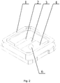
- Fig. 2 is a structural schematic diagram of a package device provided by an example of the present invention, and, as shown in Fig. 2 , based on the example described above, the first function area 4 is provided with a through hole 6, and the chip 5 is fixed in the through hole 6.
- the through hole 6 can be of various shapes, for example, a circular shape, a rectangular shape, an irregular shape, or the like.
- a fixing support made of a transparent material is provided in the through hole 6.
- the chip 5 is fixed onto the fixing support, and electrically connected to the first function area 4 and the second function area 2, respectively.
- the fixing support may be in various structural forms, for example, the fixing support is cross-shaped, ends of the fixing support are connected to an inner wall of the through hole 6, respectively, and the chip 5 is fixed at a central portion of the fixing support.
- the fixing support is arc-shaped, both ends of the fixing support are connected to the inner wall of the through hole 6, and the chip 5 is fixed at the topmost end of the fixing support.
- the fixing support and the first function area 4 can be connected by various methods, for example, adhesion, fusion welding, integral connection, or the like.
- the fixing support and the first function area 4 are integrally connected so as to enhance the strength of the connection of the fixing support and the first function area 4, avoid damage or breakage of the fixing support and the first function area 4 due to impact or collision by an external force, and prolong the service life of the package device.
- the through hole 6 is provided in the first function area 4, and the chip 5 is provided in the through hole 6, so that light generated after the chip 5 is powered on can be transmitted out directly, avoiding blocking of light of the chip 5 by the first function area 4 when the chip 5 is provided on the first function area 4, and further increasing the transmittance of light from the chip 5.
- the material of the insulation area 3 is transparent plastic.
- the transparent plastic material may be of various types, for example PMMA (polymethyl methacrylate), PS (polystyrene plastic), PC (polycarbonate), ABS, or the like.
- the material of the insulation area 3 is set to be transparent plastic, light generated after the chip 5 is powered on is partially transmitted out from the insulation area 3, and the transparent plastic increases light transmittance of the insulation area 3, reduces blocking of the light of the chip 5 by the insulation area 3, and further increases transmittance of light from the chip 5.
- the chip 5 is provided on the insulation area 3, the first function area and the second function area are connected through solder wires, and light generated after the chip 5 is powered on is transmitted out from the insulation area 3, further increasing transmittance of light from the chip 5.
- inner sidewalls of the SMD holder 1 are gradually narrowed along a direction towards the closed end of the SMD holder 1.
- the inner sidewalls of the SMD holder 1 are provided to be gradually narrowed along the direction towards the closed end of the SMD holder 1, that is to say, an opening formed by the inner sidewalls of the SMD holder 1 is gradually enlarged along a direction away from the closed end.
- the light of the chip 5 is gradually emitted along the inner sidewalls of the SMD holder 1, which increases coverage of the light emitted by the chip 5 inside the holder, thereby increasing an irradiated area of the light of the package device.
- an end of the inner sidewall of the SMD holder 1 away from the closed end of the SMD holder 1 has a section shape of a rectangle; and an end of the inner sidewall of the SMD holder 1 close to the closed end of the SMD holder 1 has a section shape of a trapezoid which has a shorter base close to the closed end of the SMD holder 1.
- the inner sidewall of the SMD holder 1 is configured to have an end with a section in the shape of a rectangle and the other end with a section in the shape of a trapezoid which has a shorter base close to the closed end of the holder, so that light of the chip 5 can be emitted in parallel along the inner sidewalls of the holder, thereby allowing the chips 5 in a plurality of SMD holders 1 to emit light in parallel along fixed directions, further allowing light of the package device to irradiate according to directions and angles preset by a user, and improving the applicability of the package device.
- the base coating can be made of various materials, for example, polysiloxanes, silanes, acrylic resins, epoxy resins, methyl carbamates, or the like, or a mixture of two or more of the above-mentioned materials.
- the inner walls of the SMD holder 1 are provided with a base coating layer, wherein the base coating can enhance both the strength of bonding between the SMD holder 1 and the pouring sealant and the strength of bonding between the chip 5 and the pouring sealant, thereby avoiding breakage of the package device due to impact by an external force, and prolonging the service life of the package device.
- the chip 5 is provided with fluorescent powder.
- the chip 5 is provided thereon with fluorescent powder, which makes the colors of the chip 5 combined better to improve softness and brightness of lamplight and avoid irritation to human eyes by the lamplight so as to make people feel comfortable when seeing the light and to improve the comfort of people during use.
- the user also can provide fluorescent powder of different colors according to needs so that the lamplight has different colors, improving the applicability of the package device.
- the sidewalls of the SMD holder 1 are connected integrally to the closed end of the SMD holder.
- the sidewalls and the closed end of the SMD holder 1 are provided to be connected integrally, thus the strength of the connection of the sidewalls and the closed end of the SMD holder can be enhanced, thereby avoiding damage or breakage thereof due to impact by an external force, and prolonging the service life of the SMD holder 1.
- the first function area 4, the insulation area 3, and the second function area 2 are connected integrally.
- the first function area 4, the insulation area 3, and the second function area 2 are provided to be connected integrally, thus the strength of the connection of the first function area 4, the insulation area 3 and the second function area 2 can be enhanced, thereby avoiding damage or breakage thereof due to impact by an external force, and prolonging the service life of the SMD holder 1.
Landscapes
- Structures Or Materials For Encapsulating Or Coating Semiconductor Devices Or Solid State Devices (AREA)
- Packaging Frangible Articles (AREA)
- Led Device Packages (AREA)
Description
- The present invention relates to the technical field of lamp beads, and particularly to a package device.
- SMD, which is the abbreviation of Surface Mounted Device, is one of SMT (Surface Mount Technology) components. In a primary stage of production of an electronic circuit board, through hole assembly is carried out completely manually. After the first batch of automated machines have been launched, some simple pin elements can be placed thereby, however, complicated elements still need to be placed manually for wave soldering. Its assembly density is high, and an electronic product obtained has a small volume, the volume and weight of a surface mounted element are only about 1/10 of those of a traditional element mounted by insertion, so it has a light weight, high reliability, strong shock resistance, low soldering defect rate, and excellent high frequency characteristics, reduces electromagnetic and radio-frequency interference, is easy to achieve automation, has high production efficiency, reduces cost by up to 30% to 50%, and saves materials, energy, devices, manual labor, time, and so on.
- A micro SMD is a standard thin product. An SMD chip has a surface with solder bumps. Steps of the production process of the micro SMD comprise fabrication of a standard wafer, re-passivation of the wafer, deposition of eutectic solder bumps on an I/O bonding pad, back grinding (only used for thin products), coating of a protective package, testing by a wafer selection platform, laser labeling, packing into a form of tape and reel, and final assembly on a PCB by using a standard surface mount technology (SMT). The micro SMD is a wafer-level chip scale package (WLCSP), which has the following features: a package size identical with a bare chip size; the smallest I/O pin; no need of underfill material; a wiring spacing of 0.5 mm; and no need of interposer between a chip and a PCB.
- An SMD holder is configured to fix a chip to be packaged into a lamp bead. An SMD holder in the prior art is a hollow housing with one end opened and has sidewalls made from a nontransparent material. The bottom of the holder is sequentially divided into a first function area, an insulation area, and a second function area along a direction perpendicular to the sidewalls of the holder. The insulation area is made from a nontransparent material, and the first function area and the second function area adopt metal materials. The chip is fixed on the first function area and electrically connected to the first function area and the second function area, respectively, by solder wires, and the first function area and the second function area are electrically connected to a positive electrode and a negative electrode of a power source, respectively. However, the SMD holder in the prior art, during use, has a lower light transmittance after the chip is powered on.
- Document
US 2010/032709 A1 presents an SMD diode holding structure including a plastic housing and a plurality of metal holders. The metal holder has a base portion and a connecting pin portion. The top and bottom surfaces of the base portion are exposed to a function area and a notch. The top surface of one base portion in the function area is connected with an LED chip, and the bottom surface of another base portion in the notch is connected with the anti-ESD chip. The LED chip, the anti-ESD chip, and the base portion are connected with a conductive wire. The function area is covered with a first sealing compound, and the notch is covered with a second sealing compound. - Document
WO 2007/127029 A2 presents a light emitting diode including a package support and a semiconductor chip on the package support, with the chip including an active region that emits light in the visible portion of the spectrum. Metal contacts are in electrical communication with the chip on the package. A substantially transparent encapsulant covers the chip in the package. A phosphor in the encapsulant emits a frequency in the visible spectrum different from the frequency emitted by the chip and in response to the wavelength emitted by the chip. - Document
JP H07 235696 A - An object of the present invention is to provide a package device to address the technical problem of low transmittance of light from a chip existing in the prior art.
- The package device according to
claim 1 provided by the present invention comprises an SMD holder, wherein the SMD holder is a hollow housing with one end opened; and the material of sidewalls of the SMD holder is transparent plastic. - Further, the package device further comprises a light emitting chip; a first function area, an insulation area, and a second function area are provided sequentially on an end surface of a closed end of the SMD holder; the chip is provided in the SMD holder; the chip is electrically connected to the first function area and the second function area, respectively. An area ratio of the first function area, the insulation area, and the second function area is 1∼5:1:1, optionally, the area ratio of the first function area, the insulation area, and the second function area is 3∼5:2:1.
- Further, the first function area is provided with a through hole; and the chip is fixed in the through hole onto a fixing support of a transparent material, the fixing support being connected by its ends to an inner wall of the through hole.
- Further, the material of the insulation area may be transparent plastic.
- Further, inner sidewalls of the SMD holder may be gradually narrowed along a direction towards a closed end of the SMD holder.
- Further, inner walls of the SMD holder may be provided with base coating. Further, the chip may be provided thereon with fluorescent powder.
- Further, the sidewalls of the SMD holder are connected integrally to the closed end of the SMD holder.
- Further, the first function area, the insulation area, and the second function area are connected integrally.
- In the package device provided by the present invention, a transparent material is provided as the material of the sidewalls of the SMD holder, and light generated after the chip is powered on can be partially transmitted out through the sidewalls of the SMD holder, avoiding blocking of the light generated after the chip is powered on by the sidewalls of the SMD holder, thereby increasing transmittance of light from the chip.
- In order to illustrate the technical solutions of specific embodiments of the present invention or the prior art more clearly, accompanying drawings required for use in the description of the specific embodiments or the prior art will be introduced briefly below. Obviously, the drawings described below are illustrative of some embodiments of the present invention, and those skilled in the art could derive other drawings from these drawings without any inventive efforts.
-
Fig. 1 is a structural schematic diagram of a package device provided by an example useful for understanding the invention. -
Fig. 2 is a structural schematic diagram of a package device provided by an example of the present invention. -
Fig. 3 is a structural schematic diagram of a package device provided by another example useful for understanding the invention. -
- 1: SMD holder; 2: second function area: 3: insulation area 4: first function area: 5: chip; 6: through hole
- Technical solutions of the present invention will be described below clearly and fully with reference to the drawings, and it is apparent that the examples described are some, but not all of the examples of the present invention. All the other examples obtained by those skilled in the art from the examples of the present invention without any inventive efforts fall within the scope of the present invention.
- In the description of the present invention, it should be noted that orientation or positional relations indicated by the terms such as "center", "up", "down", "left", "right", "vertical", "horizontal", "inside", "outside" and the like are the orientation or positional relations based on those shown in the drawings, only for facilitating describing the present invention and simplifying the description, rather than indicating or implying that the related devices or elements must have a particular orientation or must be constructed or operated in the particular orientation, and therefore should not be construed as limiting the present invention. In addition, terms such as "first", "second", and "third" are only for the purpose of description, and should not be understood as indicating or implying to have importance in relativity.
- In the description of the present invention, it should be noted that, unless otherwise expressly specified or defined, the terms "mounted", "coupled", and "connected" should be understood broadly, for example, a connection may be a fixed connection, or a detachable connection, or an integral connection; may be a mechanical connection or an electric connection, or may be a direct connection, or an indirect connection via an intermediate media, or internal communication between two elements. The specific meanings of the above-mentioned terms in the present invention could be understood by those skilled in the art according to specific situations.
-
Fig. 1 is a structural schematic diagram of a package device provided by an example useful for understanding the invention; as shown inFig. 1 , the package device provided by the example comprises anSMD holder 1, wherein theSMD holder 1 is a hollow housing with one end opened; and the material of sidewalls of theSMD holder 1 is transparent plastic. - Here, the material of the sidewalls of the
SMD holder 1 can be any type of transparent plastics, for example PMMA (polymethyl methacrylate), PS (polystyrene plastic), PC (polycarbonate), ABS, or the like. - In the package device provided by the example, a transparent material is provided as the material of the sidewalls of the
SMD holder 1, and light generated after achip 5 is powered on can be partially transmitted out through the sidewalls of theSMD holder 1, avoiding blocking of the light generated after thechip 5 is powered on by the sidewalls of theSMD holder 1, thereby increasing transmittance of light from thechip 5, so as to improve the light transmittance of the SMD holder. - As shown in
Fig. 1 , based on the example described above, the package device further comprises thechip 5; afirst function area 4, aninsulation area 3, and asecond function area 2 are provided sequentially on an end surface of a closed end of theSMD holder 1; thechip 5 is provided in theSMD holder 1 and located on thefirst function area 4; thechip 5 is electrically connected to thefirst function area 4 and thesecond function area 2, respectively; and an area ratio of thefirst function area 4, theinsulation area 3, and thesecond function area 2 is 1∼5:1:1. Optionally, the area ratio of thefirst function area 4, theinsulation area 3, and thesecond function area 2 may be 3∼5:2:1 - Here, the area ratio of the
first function area 4, theinsulation area 3, and thesecond function area 2 may be any value in the range of 1∼5:1:1, for example, 1:1:1, 2:1:1 or 5:1:1. Preferably, the area ratio of thefirst function area 4, theinsulation area 3, and thesecond function area 2 is 2:1:1. It is experimentally testified that when the area ratio of thefirst function area 4, theinsulation area 3, and thesecond function area 2 is 2:1:1, the transmittance of light from thechip 5 is higher, while thechip 5 is fixed in a more stable manner to thefirst function area 4. Optionally, the area ratio of thefirst function area 4, theinsulation area 3, and thesecond function area 2 may be any value in the range of 3∼5:2:1, for example, 3:2:1, 4:2:1 or 5:2:1. Preferably, the area ratio of thefirst function area 4, theinsulation area 3, and thesecond function area 2 is 4:2:1. It is experimentally testified that when the area ratio of thefirst function area 4, theinsulation area 3, and thesecond function area 2 is 4:2:1, the transmittance of light from thechip 5 is higher, while thechip 5 is fixed in a more stable manner to thefirst function area 4. - The
first function area 4, theinsulation area 3, and thesecond function area 2 can have various shapes, for example, a rectangular shape, an irregular shape, or the like. Preferably, each of thefirst function area 4, theinsulation area 3 and thesecond function area 2 is of a rectangular shape, and a width ratio of thefirst function area 4, theinsulation area 3 and thesecond function area 2 is 1∼5:1:1 or optionally 3∼5:2:1. A regular shape can be conveniently machined and manufactured by a user. - The material of the
insulation area 3 may be transparent plastic, for example PMMA (polymethyl methacrylate), PS (polystyrene plastic), PC (polycarbonate), ABS, or the like. The material ofinsulation area 3 may also be nontransparent plastic, for example PE (polyethylene), PP (polypropylene), or the like. Preferably, theinsulation area 3 is made of transparent plastic so that light generated after thechip 5 is powered on is partially transmitted out from theinsulation area 3, and the transparent plastic increases light transmittance of theinsulation area 3, reduces blocking of the light from thechip 5 by theinsulation area 3, and increases transmittance of light from thechip 5. - The
first function area 4, theinsulation area 3 and thesecond function area 2 can be connected by various methods, for example adhesion, soldering, integral connection, or the like. Preferably, thefirst function area 4, theinsulation area 3, and thesecond function area 2 are integrally connected so as to enhance the strength of the connection of thefirst function area 4, theinsulation area 3 and thesecond function area 2, avoid damage or breakage thereof due to impact by an external force, and prolong the service life of theSMD holder 1. - Moreover, the
chip 5 can be electrically connected by means of welding to thefirst function area 4 and thesecond function area 2, respectively. - In the present example, the area ratio of the
first function area 4, theinsulation area 3, and thesecond function area 2 is set to be 1∼5:1:1, and it is experimentally testified that when the area ratio of thefirst function area 4, theinsulation area 3, and thesecond function area 2 is set to be 1∼5:1:1, the transparency of thechip 5 can be further increased while thechip 5 is fixed firmly onto thefirst function area 4. -
Fig. 2 is a structural schematic diagram of a package device provided by an example of the present invention, and, as shown inFig. 2 , based on the example described above, thefirst function area 4 is provided with a throughhole 6, and thechip 5 is fixed in the throughhole 6. - Here, the through
hole 6 can be of various shapes, for example, a circular shape, a rectangular shape, an irregular shape, or the like. - Also, a fixing support made of a transparent material is provided in the through
hole 6. Thechip 5 is fixed onto the fixing support, and electrically connected to thefirst function area 4 and thesecond function area 2, respectively. The fixing support may be in various structural forms, for example, the fixing support is cross-shaped, ends of the fixing support are connected to an inner wall of the throughhole 6, respectively, and thechip 5 is fixed at a central portion of the fixing support. For another example, the fixing support is arc-shaped, both ends of the fixing support are connected to the inner wall of the throughhole 6, and thechip 5 is fixed at the topmost end of the fixing support. - The fixing support and the
first function area 4 can be connected by various methods, for example, adhesion, fusion welding, integral connection, or the like. Preferably, the fixing support and thefirst function area 4 are integrally connected so as to enhance the strength of the connection of the fixing support and thefirst function area 4, avoid damage or breakage of the fixing support and thefirst function area 4 due to impact or collision by an external force, and prolong the service life of the package device. - In the present example, the through
hole 6 is provided in thefirst function area 4, and thechip 5 is provided in the throughhole 6, so that light generated after thechip 5 is powered on can be transmitted out directly, avoiding blocking of light of thechip 5 by thefirst function area 4 when thechip 5 is provided on thefirst function area 4, and further increasing the transmittance of light from thechip 5. - As shown in
Figs. 1 and2 , based on the example described above, further, the material of theinsulation area 3 is transparent plastic. - Here, the transparent plastic material may be of various types, for example PMMA (polymethyl methacrylate), PS (polystyrene plastic), PC (polycarbonate), ABS, or the like.
- In the present example, the material of the
insulation area 3 is set to be transparent plastic, light generated after thechip 5 is powered on is partially transmitted out from theinsulation area 3, and the transparent plastic increases light transmittance of theinsulation area 3, reduces blocking of the light of thechip 5 by theinsulation area 3, and further increases transmittance of light from thechip 5. - As shown in
Fig. 3 , in an example not covered by the claimed invention thechip 5 is provided on theinsulation area 3, the first function area and the second function area are connected through solder wires, and light generated after thechip 5 is powered on is transmitted out from theinsulation area 3, further increasing transmittance of light from thechip 5. - As shown in
Fig. 1 , based on the example described above, further, inner sidewalls of theSMD holder 1 are gradually narrowed along a direction towards the closed end of theSMD holder 1. - In the present example, the inner sidewalls of the
SMD holder 1 are provided to be gradually narrowed along the direction towards the closed end of theSMD holder 1, that is to say, an opening formed by the inner sidewalls of theSMD holder 1 is gradually enlarged along a direction away from the closed end. The light of thechip 5 is gradually emitted along the inner sidewalls of theSMD holder 1, which increases coverage of the light emitted by thechip 5 inside the holder, thereby increasing an irradiated area of the light of the package device. - Based on the example described above, further, an end of the inner sidewall of the
SMD holder 1 away from the closed end of theSMD holder 1 has a section shape of a rectangle; and an end of the inner sidewall of theSMD holder 1 close to the closed end of theSMD holder 1 has a section shape of a trapezoid which has a shorter base close to the closed end of theSMD holder 1. - In the present example, the inner sidewall of the
SMD holder 1 is configured to have an end with a section in the shape of a rectangle and the other end with a section in the shape of a trapezoid which has a shorter base close to the closed end of the holder, so that light of thechip 5 can be emitted in parallel along the inner sidewalls of the holder, thereby allowing thechips 5 in a plurality ofSMD holders 1 to emit light in parallel along fixed directions, further allowing light of the package device to irradiate according to directions and angles preset by a user, and improving the applicability of the package device. - Based on the example described above, further inner walls of the
SMD holder 1 are provided with base coating. - Here, the base coating can be made of various materials, for example, polysiloxanes, silanes, acrylic resins, epoxy resins, methyl carbamates, or the like, or a mixture of two or more of the above-mentioned materials.
- In the present example, after the
chip 5 is fixed inside the holder, it is necessary to put pouring sealant into the holder. The inner walls of theSMD holder 1 are provided with a base coating layer, wherein the base coating can enhance both the strength of bonding between theSMD holder 1 and the pouring sealant and the strength of bonding between thechip 5 and the pouring sealant, thereby avoiding breakage of the package device due to impact by an external force, and prolonging the service life of the package device. - Based on the example described above, further, the
chip 5 is provided with fluorescent powder. - In the present example, the
chip 5 is provided thereon with fluorescent powder, which makes the colors of thechip 5 combined better to improve softness and brightness of lamplight and avoid irritation to human eyes by the lamplight so as to make people feel comfortable when seeing the light and to improve the comfort of people during use. The user also can provide fluorescent powder of different colors according to needs so that the lamplight has different colors, improving the applicability of the package device. - As shown in
Figs. 1 and2 , based on the example described above, further, the sidewalls of theSMD holder 1 are connected integrally to the closed end of the SMD holder. - In the present example, the sidewalls and the closed end of the
SMD holder 1 are provided to be connected integrally, thus the strength of the connection of the sidewalls and the closed end of the SMD holder can be enhanced, thereby avoiding damage or breakage thereof due to impact by an external force, and prolonging the service life of theSMD holder 1. - As shown in
Figs. 1 and2 , based on the example described above, further, thefirst function area 4, theinsulation area 3, and thesecond function area 2 are connected integrally. - In the present example, the
first function area 4, theinsulation area 3, and thesecond function area 2 are provided to be connected integrally, thus the strength of the connection of thefirst function area 4, theinsulation area 3 and thesecond function area 2 can be enhanced, thereby avoiding damage or breakage thereof due to impact by an external force, and prolonging the service life of theSMD holder 1. - Finally, it should be noted that the above-mentioned examples are merely used to describe the technical solutions of the present invention and are not intended to limit the invention.
Claims (9)
- A package device, comprising a Surface Mounted Device, SMD, holder (1);
wherein the SMD holder (1) is a hollow housing with one end opened; and the material of sidewalls of the SMD holder (1) is transparent plastic; the device further comprising a light emitting chip (5);
wherein a first function area (4), an insulation area (3), and a second function area (2) are provided sequentially on an end surface of a closed end of the SMD holder (1); wherein the chip (5) is electrically connected to the first function area (4) and the second function area (2), characterized in that the first function area (4) is provided with a through hole (6), wherein the chip (5) is fixed onto a fixing support of a transparent material, the fixing support being connected to an inner wall of the through hole (6), wherein
an area ratio of the first function area (4), the insulation area (3), and the second function area (2) is 1∼5:1:1. - The package device according to claim 1, characterized in that the material of the insulation area (3) is transparent plastic.
- The package device according to claim 1, characterized in that inner sidewalls of the SMD holder (1) are gradually narrowed along a direction towards a closed end of the SMD holder (1).
- The package device according to claim 1, characterized in that inner walls of the SMD holder (1) are provided with base coating.
- The package device according to claim 1, characterized in that the chip (5) is provided with fluorescent powder thereon.
- The package device according to any one of claims 1-5, characterized in that the sidewalls of the SMD holder (1) are connected integrally to a closed end of the SMD holder (1).
- The package device according to any one of claims 1-6, characterized in that the first function area (4), the insulation area (3), and the second function area (2) are connected integrally.
- The package device according to any one of claims 1-7, characterized in that the fixing support is cross-shaped, and the chip (5) is fixed at a central portion of the fixing support, wherein the ends of the fixing support are connected to the inner wall of the through hole (6).
- The package device according to any one of claims 1-7, characterized in that the fixing support is arc-shaped, and the chip (5) is fixed at the topmost end of the fixing support, wherein the ends of the fixing support are connected to the inner wall of the through hole (6) .
Applications Claiming Priority (1)
| Application Number | Priority Date | Filing Date | Title |
|---|---|---|---|
| CN201610508514.7A CN105977217A (en) | 2016-06-29 | 2016-06-29 | Packaging device |
Publications (2)
| Publication Number | Publication Date |
|---|---|
| EP3264477A1 EP3264477A1 (en) | 2018-01-03 |
| EP3264477B1 true EP3264477B1 (en) | 2021-08-25 |
Family
ID=56954501
Family Applications (1)
| Application Number | Title | Priority Date | Filing Date |
|---|---|---|---|
| EP16195252.8A Active EP3264477B1 (en) | 2016-06-29 | 2016-10-24 | Package device |
Country Status (3)
| Country | Link |
|---|---|
| US (1) | US10068826B2 (en) |
| EP (1) | EP3264477B1 (en) |
| CN (1) | CN105977217A (en) |
Citations (1)
| Publication number | Priority date | Publication date | Assignee | Title |
|---|---|---|---|---|
| JPH07235696A (en) * | 1994-02-25 | 1995-09-05 | Sharp Corp | Chip component type LED and manufacturing method thereof |
Family Cites Families (12)
| Publication number | Priority date | Publication date | Assignee | Title |
|---|---|---|---|---|
| DE10125374C1 (en) * | 2001-05-23 | 2003-01-16 | Osram Opto Semiconductors Gmbh | Housing for an electromagnetic radiation-emitting semiconductor chip and method for the production thereof |
| CN100369278C (en) * | 2003-09-19 | 2008-02-13 | 松下电器产业株式会社 | semiconductor light emitting device |
| CN2901584Y (en) * | 2006-04-03 | 2007-05-16 | 一诠精密工业股份有限公司 | Improvement of the structure of the plastic seat of the SMD light-emitting diode bracket |
| US8969908B2 (en) * | 2006-04-04 | 2015-03-03 | Cree, Inc. | Uniform emission LED package |
| EP3422425B1 (en) * | 2006-04-24 | 2022-02-23 | CreeLED, Inc. | Side-view surface mount white led |
| CN2935478Y (en) * | 2006-08-01 | 2007-08-15 | 一诠精密工业股份有限公司 | Light-transmitting surface-mounted LED holder structure |
| CN201007995Y (en) * | 2006-09-29 | 2008-01-16 | 厦门市三安光电股份有限公司 | 360 degree light-emitting LED lamp |
| TW200820463A (en) * | 2006-10-25 | 2008-05-01 | Lighthouse Technology Co Ltd | Light-improving SMD diode holder and package thereof |
| JP2008226378A (en) * | 2007-03-14 | 2008-09-25 | Matsushita Electric Ind Co Ltd | Semiconductor device, manufacturing method thereof, and optical pickup module |
| US8378287B2 (en) * | 2007-06-27 | 2013-02-19 | Koninklijke Philips Electronics N.V. | Optical sensor module including a diode laser and a substrate transparent to radiation emitted by the diode laser and a method for manufacturing an optical sensor module |
| CN201450026U (en) * | 2009-07-09 | 2010-05-05 | 深圳富达金五金塑胶有限公司 | SMD light emitting diode (LED) bracket |
| KR20160112761A (en) * | 2015-03-20 | 2016-09-28 | 삼성전자주식회사 | Light module and illumination apparatus comprising one-body type molding substrate, and method for fabricating the light module |
-
2016
- 2016-06-29 CN CN201610508514.7A patent/CN105977217A/en active Pending
- 2016-10-24 EP EP16195252.8A patent/EP3264477B1/en active Active
- 2016-10-26 US US15/334,393 patent/US10068826B2/en active Active
Patent Citations (1)
| Publication number | Priority date | Publication date | Assignee | Title |
|---|---|---|---|---|
| JPH07235696A (en) * | 1994-02-25 | 1995-09-05 | Sharp Corp | Chip component type LED and manufacturing method thereof |
Also Published As
| Publication number | Publication date |
|---|---|
| US10068826B2 (en) | 2018-09-04 |
| US20180005913A1 (en) | 2018-01-04 |
| CN105977217A (en) | 2016-09-28 |
| EP3264477A1 (en) | 2018-01-03 |
Similar Documents
| Publication | Publication Date | Title |
|---|---|---|
| US8203164B2 (en) | Light emitting diode package | |
| KR100637476B1 (en) | Side light emitting diode and method of manufacturing the same | |
| US9897266B2 (en) | Light source module and lighting apparatus including the same | |
| CN101582476B (en) | Light emitting diode and support module thereof | |
| EP2860778A1 (en) | Multi-area light emitting diode, light emitting device package including the diode and lighting apparatus including the package | |
| EP3410498A1 (en) | Light emitting element package | |
| US8405181B2 (en) | High brightness and high contrast plastic leaded chip carrier LED | |
| JP2014049764A (en) | Side emission type light-emitting diode package and manufacturing method therefor | |
| US8569080B2 (en) | Method for packaging light emitting diode | |
| EP2346103A2 (en) | Light emitting device and backlight unit | |
| US10347803B2 (en) | Light emitting device package and light system including the same | |
| TW201208138A (en) | Light emitting device package | |
| EP2978031B1 (en) | Light-emitting device for surface mounting | |
| US10068826B2 (en) | Package device | |
| EP2341284A2 (en) | Illumination device | |
| JP2007005722A (en) | Envelope for optical semiconductor element and optical semiconductor device using the same | |
| CN206179846U (en) | Packaging component | |
| KR101459555B1 (en) | Light emitting device | |
| CN206179847U (en) | Packaging component | |
| KR100792034B1 (en) | Side emitting diode | |
| CN105957839A (en) | Encapsulation device | |
| US9204558B2 (en) | Method for manufacturing packaged light emitting diode | |
| US10309586B1 (en) | Light bulb apparatus with graphite cap | |
| KR101902399B1 (en) | Light emitting device | |
| CN204901406U (en) | AC light-emitting diode lamp structure |
Legal Events
| Date | Code | Title | Description |
|---|---|---|---|
| PUAI | Public reference made under article 153(3) epc to a published international application that has entered the european phase |
Free format text: ORIGINAL CODE: 0009012 |
|
| STAA | Information on the status of an ep patent application or granted ep patent |
Free format text: STATUS: REQUEST FOR EXAMINATION WAS MADE |
|
| 17P | Request for examination filed |
Effective date: 20161024 |
|
| AK | Designated contracting states |
Kind code of ref document: A1 Designated state(s): AL AT BE BG CH CY CZ DE DK EE ES FI FR GB GR HR HU IE IS IT LI LT LU LV MC MK MT NL NO PL PT RO RS SE SI SK SM TR |
|
| AX | Request for extension of the european patent |
Extension state: BA ME |
|
| RBV | Designated contracting states (corrected) |
Designated state(s): AL AT BE BG CH CY CZ DE DK EE ES FI FR GB GR HR HU IE IS IT LI LT LU LV MC MK MT NL NO PL PT RO RS SE SI SK SM TR |
|
| RAP1 | Party data changed (applicant data changed or rights of an application transferred) |
Owner name: SHANGYOU JIAYI LIGHTING PRODUCT CO., LTD. |
|
| STAA | Information on the status of an ep patent application or granted ep patent |
Free format text: STATUS: EXAMINATION IS IN PROGRESS |
|
| 17Q | First examination report despatched |
Effective date: 20200710 |
|
| GRAP | Despatch of communication of intention to grant a patent |
Free format text: ORIGINAL CODE: EPIDOSNIGR1 |
|
| STAA | Information on the status of an ep patent application or granted ep patent |
Free format text: STATUS: GRANT OF PATENT IS INTENDED |
|
| INTG | Intention to grant announced |
Effective date: 20210324 |
|
| GRAS | Grant fee paid |
Free format text: ORIGINAL CODE: EPIDOSNIGR3 |
|
| GRAA | (expected) grant |
Free format text: ORIGINAL CODE: 0009210 |
|
| STAA | Information on the status of an ep patent application or granted ep patent |
Free format text: STATUS: THE PATENT HAS BEEN GRANTED |
|
| AK | Designated contracting states |
Kind code of ref document: B1 Designated state(s): AL AT BE BG CH CY CZ DE DK EE ES FI FR GB GR HR HU IE IS IT LI LT LU LV MC MK MT NL NO PL PT RO RS SE SI SK SM TR |
|
| REG | Reference to a national code |
Ref country code: CH Ref legal event code: EP |
|
| REG | Reference to a national code |
Ref country code: IE Ref legal event code: FG4D Ref country code: AT Ref legal event code: REF Ref document number: 1424702 Country of ref document: AT Kind code of ref document: T Effective date: 20210915 |
|
| REG | Reference to a national code |
Ref country code: DE Ref legal event code: R096 Ref document number: 602016062655 Country of ref document: DE |
|
| REG | Reference to a national code |
Ref country code: NL Ref legal event code: FP |
|
| REG | Reference to a national code |
Ref country code: LT Ref legal event code: MG9D |
|
| REG | Reference to a national code |
Ref country code: AT Ref legal event code: MK05 Ref document number: 1424702 Country of ref document: AT Kind code of ref document: T Effective date: 20210825 |
|
| PG25 | Lapsed in a contracting state [announced via postgrant information from national office to epo] |
Ref country code: HR Free format text: LAPSE BECAUSE OF FAILURE TO SUBMIT A TRANSLATION OF THE DESCRIPTION OR TO PAY THE FEE WITHIN THE PRESCRIBED TIME-LIMIT Effective date: 20210825 Ref country code: RS Free format text: LAPSE BECAUSE OF FAILURE TO SUBMIT A TRANSLATION OF THE DESCRIPTION OR TO PAY THE FEE WITHIN THE PRESCRIBED TIME-LIMIT Effective date: 20210825 Ref country code: SE Free format text: LAPSE BECAUSE OF FAILURE TO SUBMIT A TRANSLATION OF THE DESCRIPTION OR TO PAY THE FEE WITHIN THE PRESCRIBED TIME-LIMIT Effective date: 20210825 Ref country code: BG Free format text: LAPSE BECAUSE OF FAILURE TO SUBMIT A TRANSLATION OF THE DESCRIPTION OR TO PAY THE FEE WITHIN THE PRESCRIBED TIME-LIMIT Effective date: 20211125 Ref country code: AT Free format text: LAPSE BECAUSE OF FAILURE TO SUBMIT A TRANSLATION OF THE DESCRIPTION OR TO PAY THE FEE WITHIN THE PRESCRIBED TIME-LIMIT Effective date: 20210825 Ref country code: LT Free format text: LAPSE BECAUSE OF FAILURE TO SUBMIT A TRANSLATION OF THE DESCRIPTION OR TO PAY THE FEE WITHIN THE PRESCRIBED TIME-LIMIT Effective date: 20210825 Ref country code: PT Free format text: LAPSE BECAUSE OF FAILURE TO SUBMIT A TRANSLATION OF THE DESCRIPTION OR TO PAY THE FEE WITHIN THE PRESCRIBED TIME-LIMIT Effective date: 20211227 Ref country code: NO Free format text: LAPSE BECAUSE OF FAILURE TO SUBMIT A TRANSLATION OF THE DESCRIPTION OR TO PAY THE FEE WITHIN THE PRESCRIBED TIME-LIMIT Effective date: 20211125 Ref country code: ES Free format text: LAPSE BECAUSE OF FAILURE TO SUBMIT A TRANSLATION OF THE DESCRIPTION OR TO PAY THE FEE WITHIN THE PRESCRIBED TIME-LIMIT Effective date: 20210825 Ref country code: FI Free format text: LAPSE BECAUSE OF FAILURE TO SUBMIT A TRANSLATION OF THE DESCRIPTION OR TO PAY THE FEE WITHIN THE PRESCRIBED TIME-LIMIT Effective date: 20210825 |
|
| PG25 | Lapsed in a contracting state [announced via postgrant information from national office to epo] |
Ref country code: PL Free format text: LAPSE BECAUSE OF FAILURE TO SUBMIT A TRANSLATION OF THE DESCRIPTION OR TO PAY THE FEE WITHIN THE PRESCRIBED TIME-LIMIT Effective date: 20210825 Ref country code: LV Free format text: LAPSE BECAUSE OF FAILURE TO SUBMIT A TRANSLATION OF THE DESCRIPTION OR TO PAY THE FEE WITHIN THE PRESCRIBED TIME-LIMIT Effective date: 20210825 Ref country code: GR Free format text: LAPSE BECAUSE OF FAILURE TO SUBMIT A TRANSLATION OF THE DESCRIPTION OR TO PAY THE FEE WITHIN THE PRESCRIBED TIME-LIMIT Effective date: 20211126 |
|
| PG25 | Lapsed in a contracting state [announced via postgrant information from national office to epo] |
Ref country code: DK Free format text: LAPSE BECAUSE OF FAILURE TO SUBMIT A TRANSLATION OF THE DESCRIPTION OR TO PAY THE FEE WITHIN THE PRESCRIBED TIME-LIMIT Effective date: 20210825 |
|
| REG | Reference to a national code |
Ref country code: DE Ref legal event code: R097 Ref document number: 602016062655 Country of ref document: DE |
|
| REG | Reference to a national code |
Ref country code: CH Ref legal event code: PL |
|
| PG25 | Lapsed in a contracting state [announced via postgrant information from national office to epo] |
Ref country code: SM Free format text: LAPSE BECAUSE OF FAILURE TO SUBMIT A TRANSLATION OF THE DESCRIPTION OR TO PAY THE FEE WITHIN THE PRESCRIBED TIME-LIMIT Effective date: 20210825 Ref country code: SK Free format text: LAPSE BECAUSE OF FAILURE TO SUBMIT A TRANSLATION OF THE DESCRIPTION OR TO PAY THE FEE WITHIN THE PRESCRIBED TIME-LIMIT Effective date: 20210825 Ref country code: RO Free format text: LAPSE BECAUSE OF FAILURE TO SUBMIT A TRANSLATION OF THE DESCRIPTION OR TO PAY THE FEE WITHIN THE PRESCRIBED TIME-LIMIT Effective date: 20210825 Ref country code: EE Free format text: LAPSE BECAUSE OF FAILURE TO SUBMIT A TRANSLATION OF THE DESCRIPTION OR TO PAY THE FEE WITHIN THE PRESCRIBED TIME-LIMIT Effective date: 20210825 Ref country code: CZ Free format text: LAPSE BECAUSE OF FAILURE TO SUBMIT A TRANSLATION OF THE DESCRIPTION OR TO PAY THE FEE WITHIN THE PRESCRIBED TIME-LIMIT Effective date: 20210825 Ref country code: AL Free format text: LAPSE BECAUSE OF FAILURE TO SUBMIT A TRANSLATION OF THE DESCRIPTION OR TO PAY THE FEE WITHIN THE PRESCRIBED TIME-LIMIT Effective date: 20210825 |
|
| REG | Reference to a national code |
Ref country code: BE Ref legal event code: MM Effective date: 20211031 |
|
| PG25 | Lapsed in a contracting state [announced via postgrant information from national office to epo] |
Ref country code: MC Free format text: LAPSE BECAUSE OF FAILURE TO SUBMIT A TRANSLATION OF THE DESCRIPTION OR TO PAY THE FEE WITHIN THE PRESCRIBED TIME-LIMIT Effective date: 20210825 |
|
| PLBE | No opposition filed within time limit |
Free format text: ORIGINAL CODE: 0009261 |
|
| STAA | Information on the status of an ep patent application or granted ep patent |
Free format text: STATUS: NO OPPOSITION FILED WITHIN TIME LIMIT |
|
| PG25 | Lapsed in a contracting state [announced via postgrant information from national office to epo] |
Ref country code: LU Free format text: LAPSE BECAUSE OF NON-PAYMENT OF DUE FEES Effective date: 20211024 Ref country code: BE Free format text: LAPSE BECAUSE OF NON-PAYMENT OF DUE FEES Effective date: 20211031 |
|
| 26N | No opposition filed |
Effective date: 20220527 |
|
| PG25 | Lapsed in a contracting state [announced via postgrant information from national office to epo] |
Ref country code: SI Free format text: LAPSE BECAUSE OF FAILURE TO SUBMIT A TRANSLATION OF THE DESCRIPTION OR TO PAY THE FEE WITHIN THE PRESCRIBED TIME-LIMIT Effective date: 20210825 Ref country code: LI Free format text: LAPSE BECAUSE OF NON-PAYMENT OF DUE FEES Effective date: 20211031 Ref country code: CH Free format text: LAPSE BECAUSE OF NON-PAYMENT OF DUE FEES Effective date: 20211031 |
|
| PG25 | Lapsed in a contracting state [announced via postgrant information from national office to epo] |
Ref country code: IE Free format text: LAPSE BECAUSE OF NON-PAYMENT OF DUE FEES Effective date: 20211024 |
|
| PG25 | Lapsed in a contracting state [announced via postgrant information from national office to epo] |
Ref country code: HU Free format text: LAPSE BECAUSE OF FAILURE TO SUBMIT A TRANSLATION OF THE DESCRIPTION OR TO PAY THE FEE WITHIN THE PRESCRIBED TIME-LIMIT; INVALID AB INITIO Effective date: 20161024 |
|
| PG25 | Lapsed in a contracting state [announced via postgrant information from national office to epo] |
Ref country code: CY Free format text: LAPSE BECAUSE OF FAILURE TO SUBMIT A TRANSLATION OF THE DESCRIPTION OR TO PAY THE FEE WITHIN THE PRESCRIBED TIME-LIMIT Effective date: 20210825 |
|
| PG25 | Lapsed in a contracting state [announced via postgrant information from national office to epo] |
Ref country code: MK Free format text: LAPSE BECAUSE OF FAILURE TO SUBMIT A TRANSLATION OF THE DESCRIPTION OR TO PAY THE FEE WITHIN THE PRESCRIBED TIME-LIMIT Effective date: 20210825 |
|
| PG25 | Lapsed in a contracting state [announced via postgrant information from national office to epo] |
Ref country code: TR Free format text: LAPSE BECAUSE OF FAILURE TO SUBMIT A TRANSLATION OF THE DESCRIPTION OR TO PAY THE FEE WITHIN THE PRESCRIBED TIME-LIMIT Effective date: 20210825 |
|
| PG25 | Lapsed in a contracting state [announced via postgrant information from national office to epo] |
Ref country code: MT Free format text: LAPSE BECAUSE OF FAILURE TO SUBMIT A TRANSLATION OF THE DESCRIPTION OR TO PAY THE FEE WITHIN THE PRESCRIBED TIME-LIMIT Effective date: 20210825 |
|
| REG | Reference to a national code |
Ref country code: DE Ref legal event code: R079 Ref document number: 602016062655 Country of ref document: DE Free format text: PREVIOUS MAIN CLASS: H01L0033480000 Ipc: H10H0020850000 |
|
| PGFP | Annual fee paid to national office [announced via postgrant information from national office to epo] |
Ref country code: NL Payment date: 20251023 Year of fee payment: 10 |
|
| PGFP | Annual fee paid to national office [announced via postgrant information from national office to epo] |
Ref country code: DE Payment date: 20251020 Year of fee payment: 10 |
|
| PGFP | Annual fee paid to national office [announced via postgrant information from national office to epo] |
Ref country code: GB Payment date: 20251024 Year of fee payment: 10 |
|
| PGFP | Annual fee paid to national office [announced via postgrant information from national office to epo] |
Ref country code: IT Payment date: 20251031 Year of fee payment: 10 |
|
| PGFP | Annual fee paid to national office [announced via postgrant information from national office to epo] |
Ref country code: FR Payment date: 20251017 Year of fee payment: 10 |