EP3264465A1 - Bendable display device - Google Patents
Bendable display device Download PDFInfo
- Publication number
- EP3264465A1 EP3264465A1 EP17178277.4A EP17178277A EP3264465A1 EP 3264465 A1 EP3264465 A1 EP 3264465A1 EP 17178277 A EP17178277 A EP 17178277A EP 3264465 A1 EP3264465 A1 EP 3264465A1
- Authority
- EP
- European Patent Office
- Prior art keywords
- display panel
- area
- display
- cutout
- display device
- Prior art date
- Legal status (The legal status is an assumption and is not a legal conclusion. Google has not performed a legal analysis and makes no representation as to the accuracy of the status listed.)
- Granted
Links
Images









Classifications
-
- G—PHYSICS
- G02—OPTICS
- G02F—OPTICAL DEVICES OR ARRANGEMENTS FOR THE CONTROL OF LIGHT BY MODIFICATION OF THE OPTICAL PROPERTIES OF THE MEDIA OF THE ELEMENTS INVOLVED THEREIN; NON-LINEAR OPTICS; FREQUENCY-CHANGING OF LIGHT; OPTICAL LOGIC ELEMENTS; OPTICAL ANALOGUE/DIGITAL CONVERTERS
- G02F1/00—Devices or arrangements for the control of the intensity, colour, phase, polarisation or direction of light arriving from an independent light source, e.g. switching, gating or modulating; Non-linear optics
- G02F1/01—Devices or arrangements for the control of the intensity, colour, phase, polarisation or direction of light arriving from an independent light source, e.g. switching, gating or modulating; Non-linear optics for the control of the intensity, phase, polarisation or colour
- G02F1/13—Devices or arrangements for the control of the intensity, colour, phase, polarisation or direction of light arriving from an independent light source, e.g. switching, gating or modulating; Non-linear optics for the control of the intensity, phase, polarisation or colour based on liquid crystals, e.g. single liquid crystal display cells
- G02F1/133—Constructional arrangements; Operation of liquid crystal cells; Circuit arrangements
- G02F1/1333—Constructional arrangements; Manufacturing methods
- G02F1/133305—Flexible substrates, e.g. plastics, organic film
-
- G—PHYSICS
- G02—OPTICS
- G02F—OPTICAL DEVICES OR ARRANGEMENTS FOR THE CONTROL OF LIGHT BY MODIFICATION OF THE OPTICAL PROPERTIES OF THE MEDIA OF THE ELEMENTS INVOLVED THEREIN; NON-LINEAR OPTICS; FREQUENCY-CHANGING OF LIGHT; OPTICAL LOGIC ELEMENTS; OPTICAL ANALOGUE/DIGITAL CONVERTERS
- G02F1/00—Devices or arrangements for the control of the intensity, colour, phase, polarisation or direction of light arriving from an independent light source, e.g. switching, gating or modulating; Non-linear optics
- G02F1/01—Devices or arrangements for the control of the intensity, colour, phase, polarisation or direction of light arriving from an independent light source, e.g. switching, gating or modulating; Non-linear optics for the control of the intensity, phase, polarisation or colour
- G02F1/13—Devices or arrangements for the control of the intensity, colour, phase, polarisation or direction of light arriving from an independent light source, e.g. switching, gating or modulating; Non-linear optics for the control of the intensity, phase, polarisation or colour based on liquid crystals, e.g. single liquid crystal display cells
- G02F1/133—Constructional arrangements; Operation of liquid crystal cells; Circuit arrangements
- G02F1/1333—Constructional arrangements; Manufacturing methods
- G02F1/1345—Conductors connecting electrodes to cell terminals
- G02F1/13458—Terminal pads
-
- G—PHYSICS
- G06—COMPUTING OR CALCULATING; COUNTING
- G06F—ELECTRIC DIGITAL DATA PROCESSING
- G06F1/00—Details not covered by groups G06F3/00 - G06F13/00 and G06F21/00
- G06F1/16—Constructional details or arrangements
- G06F1/1613—Constructional details or arrangements for portable computers
- G06F1/1633—Constructional details or arrangements of portable computers not specific to the type of enclosures covered by groups G06F1/1615 - G06F1/1626
- G06F1/1637—Details related to the display arrangement, including those related to the mounting of the display in the housing
- G06F1/1652—Details related to the display arrangement, including those related to the mounting of the display in the housing the display being flexible, e.g. mimicking a sheet of paper, or rollable
-
- H—ELECTRICITY
- H05—ELECTRIC TECHNIQUES NOT OTHERWISE PROVIDED FOR
- H05K—PRINTED CIRCUITS; CASINGS OR CONSTRUCTIONAL DETAILS OF ELECTRIC APPARATUS; MANUFACTURE OF ASSEMBLAGES OF ELECTRICAL COMPONENTS
- H05K1/00—Printed circuits
- H05K1/02—Details
- H05K1/0277—Bendability or stretchability details
- H05K1/028—Bending or folding regions of flexible printed circuits
-
- H—ELECTRICITY
- H10—SEMICONDUCTOR DEVICES; ELECTRIC SOLID-STATE DEVICES NOT OTHERWISE PROVIDED FOR
- H10K—ORGANIC ELECTRIC SOLID-STATE DEVICES
- H10K59/00—Integrated devices, or assemblies of multiple devices, comprising at least one organic light-emitting element covered by group H10K50/00
- H10K59/10—OLED displays
- H10K59/12—Active-matrix OLED [AMOLED] displays
- H10K59/129—Chiplets
-
- H—ELECTRICITY
- H10—SEMICONDUCTOR DEVICES; ELECTRIC SOLID-STATE DEVICES NOT OTHERWISE PROVIDED FOR
- H10K—ORGANIC ELECTRIC SOLID-STATE DEVICES
- H10K77/00—Constructional details of devices covered by this subclass and not covered by groups H10K10/80, H10K30/80, H10K50/80 or H10K59/80
- H10K77/10—Substrates, e.g. flexible substrates
- H10K77/111—Flexible substrates
-
- G—PHYSICS
- G06—COMPUTING OR CALCULATING; COUNTING
- G06F—ELECTRIC DIGITAL DATA PROCESSING
- G06F1/00—Details not covered by groups G06F3/00 - G06F13/00 and G06F21/00
- G06F1/16—Constructional details or arrangements
- G06F1/1601—Constructional details related to the housing of computer displays, e.g. of CRT monitors, of flat displays
-
- G—PHYSICS
- G06—COMPUTING OR CALCULATING; COUNTING
- G06F—ELECTRIC DIGITAL DATA PROCESSING
- G06F1/00—Details not covered by groups G06F3/00 - G06F13/00 and G06F21/00
- G06F1/16—Constructional details or arrangements
- G06F1/1613—Constructional details or arrangements for portable computers
- G06F1/1615—Constructional details or arrangements for portable computers with several enclosures having relative motions, each enclosure supporting at least one I/O or computing function
- G06F1/1616—Constructional details or arrangements for portable computers with several enclosures having relative motions, each enclosure supporting at least one I/O or computing function with folding flat displays, e.g. laptop computers or notebooks having a clamshell configuration, with body parts pivoting to an open position around an axis parallel to the plane they define in closed position
-
- G—PHYSICS
- G09—EDUCATION; CRYPTOGRAPHY; DISPLAY; ADVERTISING; SEALS
- G09G—ARRANGEMENTS OR CIRCUITS FOR CONTROL OF INDICATING DEVICES USING STATIC MEANS TO PRESENT VARIABLE INFORMATION
- G09G2380/00—Specific applications
- G09G2380/02—Flexible displays
-
- H—ELECTRICITY
- H10—SEMICONDUCTOR DEVICES; ELECTRIC SOLID-STATE DEVICES NOT OTHERWISE PROVIDED FOR
- H10D—INORGANIC ELECTRIC SEMICONDUCTOR DEVICES
- H10D86/00—Integrated devices formed in or on insulating or conducting substrates, e.g. formed in silicon-on-insulator [SOI] substrates or on stainless steel or glass substrates
- H10D86/40—Integrated devices formed in or on insulating or conducting substrates, e.g. formed in silicon-on-insulator [SOI] substrates or on stainless steel or glass substrates characterised by multiple TFTs
- H10D86/411—Integrated devices formed in or on insulating or conducting substrates, e.g. formed in silicon-on-insulator [SOI] substrates or on stainless steel or glass substrates characterised by multiple TFTs characterised by materials, geometry or structure of the substrates
-
- H—ELECTRICITY
- H10—SEMICONDUCTOR DEVICES; ELECTRIC SOLID-STATE DEVICES NOT OTHERWISE PROVIDED FOR
- H10D—INORGANIC ELECTRIC SEMICONDUCTOR DEVICES
- H10D86/00—Integrated devices formed in or on insulating or conducting substrates, e.g. formed in silicon-on-insulator [SOI] substrates or on stainless steel or glass substrates
- H10D86/40—Integrated devices formed in or on insulating or conducting substrates, e.g. formed in silicon-on-insulator [SOI] substrates or on stainless steel or glass substrates characterised by multiple TFTs
- H10D86/441—Interconnections, e.g. scanning lines
-
- H—ELECTRICITY
- H10—SEMICONDUCTOR DEVICES; ELECTRIC SOLID-STATE DEVICES NOT OTHERWISE PROVIDED FOR
- H10D—INORGANIC ELECTRIC SEMICONDUCTOR DEVICES
- H10D86/00—Integrated devices formed in or on insulating or conducting substrates, e.g. formed in silicon-on-insulator [SOI] substrates or on stainless steel or glass substrates
- H10D86/40—Integrated devices formed in or on insulating or conducting substrates, e.g. formed in silicon-on-insulator [SOI] substrates or on stainless steel or glass substrates characterised by multiple TFTs
- H10D86/60—Integrated devices formed in or on insulating or conducting substrates, e.g. formed in silicon-on-insulator [SOI] substrates or on stainless steel or glass substrates characterised by multiple TFTs wherein the TFTs are in active matrices
-
- H—ELECTRICITY
- H10—SEMICONDUCTOR DEVICES; ELECTRIC SOLID-STATE DEVICES NOT OTHERWISE PROVIDED FOR
- H10K—ORGANIC ELECTRIC SOLID-STATE DEVICES
- H10K2102/00—Constructional details relating to the organic devices covered by this subclass
- H10K2102/301—Details of OLEDs
- H10K2102/311—Flexible OLED
-
- H—ELECTRICITY
- H10—SEMICONDUCTOR DEVICES; ELECTRIC SOLID-STATE DEVICES NOT OTHERWISE PROVIDED FOR
- H10K—ORGANIC ELECTRIC SOLID-STATE DEVICES
- H10K59/00—Integrated devices, or assemblies of multiple devices, comprising at least one organic light-emitting element covered by group H10K50/00
- H10K59/10—OLED displays
-
- H—ELECTRICITY
- H10—SEMICONDUCTOR DEVICES; ELECTRIC SOLID-STATE DEVICES NOT OTHERWISE PROVIDED FOR
- H10K—ORGANIC ELECTRIC SOLID-STATE DEVICES
- H10K59/00—Integrated devices, or assemblies of multiple devices, comprising at least one organic light-emitting element covered by group H10K50/00
- H10K59/10—OLED displays
- H10K59/12—Active-matrix OLED [AMOLED] displays
- H10K59/131—Interconnections, e.g. wiring lines or terminals
-
- Y—GENERAL TAGGING OF NEW TECHNOLOGICAL DEVELOPMENTS; GENERAL TAGGING OF CROSS-SECTIONAL TECHNOLOGIES SPANNING OVER SEVERAL SECTIONS OF THE IPC; TECHNICAL SUBJECTS COVERED BY FORMER USPC CROSS-REFERENCE ART COLLECTIONS [XRACs] AND DIGESTS
- Y02—TECHNOLOGIES OR APPLICATIONS FOR MITIGATION OR ADAPTATION AGAINST CLIMATE CHANGE
- Y02E—REDUCTION OF GREENHOUSE GAS [GHG] EMISSIONS, RELATED TO ENERGY GENERATION, TRANSMISSION OR DISTRIBUTION
- Y02E10/00—Energy generation through renewable energy sources
- Y02E10/50—Photovoltaic [PV] energy
- Y02E10/549—Organic PV cells
Definitions
- Exemplary embodiments of the present invention relate to a display device, and more particularly to a bendable display device.
- Display devices such as an organic light emitting device and a liquid crystal display may be manufactured by generating a plurality of layers and elements on a substrate.
- the substrate of the display device may include glass.
- a glass substrate may be relatively rigid, relatively heavy and may break.
- Display devices may include a relatively flexible substrate that is relatively light, relatively strong against impacts, and may be relatively easily deformed.
- a display device including a flexible substrate may be manufactured to bend at an edge where a pad portion to which a flexible printed circuit film (FPC) for transmitting signals is positioned, thus creating a relatively small dead space.
- FPC flexible printed circuit film
- One or more exemplary embodiments of the present invention provide a display device including a flexible substrate having increased reliability of a bending area and a pad area.
- An exemplary embodiment of the present invention provides a display device including a bendable display panel including a substrate and a plurality of pad portions on the substrate.
- the substrate includes a cutout between adjacent pad portions of the plurality of pad portions.
- the cutout may be dimensioned and positioned to at least partially isolate movement of a first pad portion from movement of a second pad portion when the bendable display panel is bent.
- the display panel may include a display area displaying an image and a non-display area adjacent to the display area.
- the plurality of pad portions may be arranged along a first direction in the non-display area, and the cutout may extend in a second direction crossing the first direction.
- the cutout may extend in the second direction from an edge of the display panel opposite the display area of the display panel.
- the display panel may include a bending area between the display area and the pad portions, and the bending area may be bendable with respect to a bending axis extending in the first direction.
- the bending area may include a plurality of wires, and the plurality of wires may extend along the second direction.
- the display panel may include a plurality of fan-outs between the pad portions and the bending area, and the cutout may extend to a region between neighboring fan-outs.
- the display device may include at least one flexible printed circuit film disposed on the pad portions.
- An integrated circuit chip may be disposed on the flexible printed circuit film.
- the cutout may penetrate the display panel in a thickness direction of the display panel.
- An exemplary embodiment of the present invention provides a display device including a display panel including a display area displaying an image and a non-display area including a plurality of pad portions. At least one flexible printed circuit film is disposed on each of the plurality of pad portions. The pad portions are arranged along a first direction. The display panel includes a cutout between adjacent pad portions of the plurality of pad portions. The cutout extends in a second direction crossing the first direction.
- the display panel may include a bending area between the display area and the pad portions, and the bending area may include a plurality of wires extending along the second direction.
- the bending area may be bendable with respect to a bending axis extending in the first direction.
- a flexible printed circuit film may be disposed on each of the pad portions.
- a driving circuit chip may be disposed on each of the flexible printed circuit films.
- the cutout may extend in the second direction from an edge of the display panel opposite the display area of the display panel.
- the display panel may include a plurality of fan-outs between the pad portions and the bending area, and the cutout may extend to a region between neighboring fan-outs.
- a plane shape of an end portion of the cutout facing the display area of the display panel may be pointed, may be polygonal or may be round.
- the cutout may penetrate the display panel in a thickness direction of the display panel.
- An exemplary embodiment of the present invention provides a display device including a display panel including a display area displaying an image and a non-display area including a pad portion.
- a flexible printed circuit film is disposed on the pad portion.
- the pad portion includes a plurality of pads arranged along a first direction.
- the display panel includes a cutout formed between adjacent pads and extending in a second direction crossing the first direction.
- the display panel may include a bending area between the display area and the pad portion, and the bending area may include a plurality of wires extending along the second direction.
- the bending area may be bendable with respect to a bending axis extending in the first direction.
- the cutout may be formed along the second direction from an edge of the display panel opposite the display area of the display panel.
- the cutout may be formed in the second direction and may extend beyond the edge of the display panel by a predetermined distance in the pad portion.
- the cutout may penetrate the display panel in a thickness direction of the display panel.
- the cutout may be formed along a thickness direction of the display panel from a top surface of the display panel to a depth above a bottom surface of the display panel.
- the display panel may include a substrate.
- the pad portion may be positioned on a first side of the substrate, and a protection film may be positioned on a second side of the substrate.
- the cutout may penetrate the substrate and may be formed through part of the protection film.
- application of a force to the wires in the bending area in a direction different from a bending direction may be controlled, and generation of cracks of the wires in the bending area may be reduced or prevented.
- a generation of waviness may be reduced or prevented in the pad area of the display panel.
- FIG. 1 is a top plan view of a display device that is not bent according to an exemplary embodiment of the present invention.
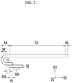
- FIG. 2 is a side view of the display device shown in FIG. 1 that is bent.
- the display device may include a display panel 10 and at least one flexible printed circuit film 50 connected to the display panel 10.
- the display panel 10 may include a display area (DA) displaying an image, and a non-display area (NA) in which elements and/or wires (W) generating various signals applied to the display area (DA) and/or transmitting the various signals are disposed.
- the non-display area may be adjacent to the display area (DA).
- pixels PX may be arranged in a matrix in the display area (DA) of the display panel 10.
- signal lines including gate lines and data lines may be disposed.
- the gate lines may extend in a first direction D1 (e.g., a row direction), and the data lines may extend in a second direction D2 (e.g., a column direction) crossing the first direction D1.
- the gate lines may extend in the same direction as the data lines, for example, in the second direction D2.
- At least one gate line and at least one data line may be connected to each of the pixels PX.
- Each pixel PX may receive a gate signal and a data signal from the signal lines.
- driving voltage lines may extend, for example, in the second direction D2 and may transmit a driving voltage to the pixel PX.
- the driving voltage lines may be positioned in the display area (DA).
- the non-display area (NA) of the display panel 10 may include a pad area (PA) including pad portions (PP) receiving signals from outside of the display panel 10.
- Each of the pad portions (PP) may include pads arranged, for example, in the first direction D1 at a predetermined interval.
- the pad portions (PP) may be disposed on an edge of the display panel 10 along the first direction D1 at a predetermined interval.
- a cutout (C) may be formed between the neighboring pad portions (PP). As an example, before the display panel 10 is bent, the cutouts (C) may be formed in the second direction D2 toward the display area (DA) from the edge of the display panel 10.
- a formation direction of the cutout (C) is not limited to the second direction D2, and the cutout (C) may be formed in a direction that is oblique to the second direction D2.
- the cutout (C) may fully penetrate the display panel 10 in a third direction D3 that is a thickness direction of the display panel 10.
- neighboring pad portions (PP) may be partially separated from each other along the first direction D1 by the cutouts (C).
- C the cutouts
- a pad portion of the pad portions (PP) is bent, it might not affect a neighboring pad portion (PP).
- stress applied to an area near a pad portion of the pad portions (PP) may be reduced or eliminated.
- stress on wires (W) positioned in a bending area (BA) of the display panel 10 may be reduced or eliminated and thus an occurrence of cracks in the wires (W) may be reduced or eliminated.
- the cutouts (C) may be formed by cutting the display panel 10 by use of laser beams or a knife, or by etching the display panel 10 through a photolithography process.
- a first end of the flexible printed circuit film 50 may be connected to each pad portion (PP).
- An anisotropic conductive film may be disposed between the pad portions (PP) and the flexible printed circuit film 50.
- the flexible printed circuit film 50 may include a second end connected to a printed circuit board and transmitting signals such as control signals or image data.
- a driving device generating and/or processing various signals for driving the display panel 10 may be positioned in the non-display area (NA) of the display panel 10 (e.g., on the flexible printed circuit film 50).
- the driving device may be disposed on the printed circuit board.
- the driving device may include a data driver applying a data signal to the data line, a gate driver applying a gate signal to the gate line, and a signal controller controlling the data driver and the gate driver.
- the data driver may be an integrated circuit chip of a plurality of integrated circuit chips 500 disposed on the flexible printed circuit film 50.
- Each of the integrated circuit chips 500 may be connected as a tape carrier package to a pad portion of the pad portions (PP).
- the data driver may be positioned between the display area (DA) and the pad area (PA).
- the gate driver may be positioned in the non-display area (NA) on edges of the display panel 10 (e.g., on left/right sides of the display panel 10 along the first direction).
- the gate driver may be an integrated circuit chip of the integrated circuit chips 500.
- the signal controller may be an integrated circuit chip of integrated circuit chips 500 and may be connected to the printed circuit board. The signal controller may transmit control signals through the flexible printed circuit film 50.
- the display panel 10 includes the bending area (BA) between the display area (DA) and the pad area (PA).
- the bending area (BA) may an area extending along the display panel 10 in the first direction D1.
- the display panel 10 may be bent along a bending axis (X), which is substantially parallel with the first direction D1.
- the flexible printed circuit films 50 may be positioned behind the display area (DA) when the display panel 10 is bent.
- the bending area (BA) may be in the display area (DA) and the non-display area (NA); however exemplary embodiments of the present invention are not limited thereto.
- the bending area (BA) may be entirely in the non-display area (NA).
- a fan out area (FOA) may be between the bending area (BA) and the pad area (PA).
- the fan out area (FOA) may be positioned along the first direction D1.
- the fan out area (FOA) may include a plurality of fan-outs (FO).
- Wires (W) connected to the pads of the pad portions (PP) may be adjacent to the fan-outs (FO).
- the fan-outs (FO) may be positioned at a predetermined interval along the first direction D1. A separation between adjacent fan-outs (FO) may become gradually narrower along the second direction from the pad portions (PP) toward the display area (DA) of the display panel 10.
- the wires (W) may pass through the fan-out area (FOA) and the bending area (BA) and may be connected to various signal lines such as data lines.
- the wires (W) may extend in the second direction D2 in the bending area (BA) and may be substantially perpendicular to the bending axis (X).
- the cutouts (C) positioned in the pad area (PA) may extend to a region between adjacent fan-outs (FO) of the fan out area (FOA). Thus, stress applied in the fan out area (FOA) when the display panel 10 is bent may be reduced or eliminated.
- the wires (W) are not positioned in the region in which the cutouts (C) are formed.
- cutouts (C) according to an exemplary embodiment of the present invention will be described in more detail below with reference to FIG. 3 and FIG. 4 .
- FIG. 3 illustrates a comparative example of a region R1 of FIG. 1 .
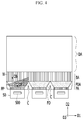
- FIG. 4 illustrates an exemplary embodiment of the region R1 of FIG. 1 .
- a flexible printed circuit film 50 on which an integrated circuit chip 500 is disposed may be connected to each pad portion (PP).
- a region near the pad portion (PP) may be folded in an undesired manner because of weight of the integrated circuit chip 500, and thus the folded region may be relatively wide.
- an adjacent pad portion of the pad portions (PP) may also be folded in a folding direction (DF).
- the folding direction (DF) may cross a bending direction (DB) of the bending area (BA).
- the wires (W) (e.g., a second wire portion 179 illustrated, for example, in FIG. 10 ) in the bending area (BA) may be configured to well withstand a stress in the bending direction (DB), but not in another direction than the bending direction (DB), and thus when stress is applied in the folding direction (DF) traversing the bending direction (DB), for example, the stress may cause the wires (W) to crack or short-circuit. Additionally, a relatively wide folding region may result in a plurality of wires (W) being damaged.
- the cutout (C) may be formed between neighboring pad portions (PP).
- the flexible printed circuit film 50 on which the integrated circuit chip 500 is disposed may be connected to a corresponding pad portion (PP), and the region near the pad portion (PP) to which the flexible printed circuit film 50 is bonded may be undesirably folded by the weight of the integrated circuit chip 500.
- the region near a pad portion of the pad portions (PP) is folded, such folding does not extend to adjacent pad portions (PP) but is blocked by the cutout (C).
- the folding may be limited to the region corresponding to one pad portion (PP), and the folding direction (DF) may substantially correspond to the bending direction (DB) of the bending area (BA).
- the cutout (C) may extend to a space between the fan-outs (FO) of the fan out area (FOA) from the edge of the display panel 10 thus further reducing an influence of folding a first pad portion on adjacent pad portions (PP).
- the cutout (C) may have a V shape (or a plane shape of a triangle) that becomes narrower and pointed at an end of the V shaped cutout closer to the display area DA of the display panel; however exemplary embodiments of the present invention are not limited thereto.
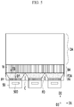
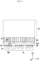
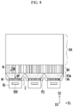
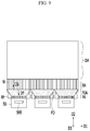
- the cutout (C) according to some exemplary embodiments of the present invention will be described in more detail below with reference to FIG. 5 to FIG. 9 .
- FIG. 5 , FIG. 6 , FIG. 7 , FIG. 8 , and FIG. 9 each respectively illustrates an exemplary embodiment of a region R1 of FIG. 1 .
- the cutout (C) may have a plane shape of a rectangle with a substantially constant width.
- the cutout (C) may have a substantially rectangular shape in which an end of the cutout (C) closest to the display area DA of the display panel is rounded.
- the cutout (C) may have a plane shape of a semicircle or may have a plane shape of a semi-ellipse.
- the cutout (C) may have a plane shape of a light bulb.
- the cutout (C) may have various shapes between the neighboring pad portions (PP), and the cutout (C) reduces or prevents the folding influence of a pad portion of the pad portions (PP) from being applied to adjacent pad portions (PP). Thus damage to the wires (W) in the bending area (BA) may be reduced or eliminated. Cutouts (C) may be formed between each pair of adjacent pad portions (PP), or cutouts (C) between some pad portions (PP) may be omitted.
- a stacked configuration of the display device will be described below in more detail with reference to the pixel PX of the non-display area (NA) and the display area (DA) in which the bending area (BA) and the pad area (PA) are provided.
- FIG. 10 illustrates an exemplary embodiment of a cross-section with respect to a line X-X' in FIG. 1 .
- FIG. 11 illustrates an exemplary embodiment of a cross-section with respect to a line XI-XI' in FIG. 1 .
- FIG. 12 illustrates an exemplary embodiment of a cross-section of a pixel area in FIG. 1 .
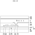
- FIG. 13 illustrates another exemplary embodiment of a cross-section of a pixel area in FIG. 1 .
- FIG. 12 exemplifies a case in which the display device is an organic light emitting device
- FIG. 13 exemplifies a case in which the display device is a liquid crystal display.
- Configurations of FIG. 10 and FIG. 11 may be applied to display devices according to other exemplary embodiments of the present invention, regardless of the type of the display device.
- An organic light emitting device according to an exemplary embodiment of the present invention will be described below in more detail with reference to FIG. 10 , FIG. 11 , and FIG. 12 .
- Technical features that are the same as those described above may be omitted, and thus duplicative descriptions may be omitted.
- the display panel 10 may include a substrate 110 and a plurality of layers disposed on the substrate 110.
- the substrate 110 may be a flexible substrate including a transparent polymer film.
- the substrate 110 may include a plastic such as polyimide, polyamide, or polyethylene terephthalate.
- the substrate 110 may include a buffer layer.
- the buffer layer may reduce or prevent a penetration of impurities or moisture into the substrate 110.
- the buffer layer may be formed on substantially the entire substrate 110, except for in the bending area (BA).
- a semiconductor 131 of a transistor may be disposed on the substrate 110.
- a gate insulating layer 140 may be disposed on the semiconductor 131.
- the semiconductor 131 may include a source region, a drain region, and a channel region between the source and drain regions.
- the semiconductor 131 may include polysilicon, an oxide semiconductor, or amorphous silicon.
- the gate insulating layer 140 may be formed by stacking inorganic insulating materials such as a silicon oxide or a silicon nitride. The gate insulating layer 140 need not be provided in the bending area (BA).
- the gate insulating layer 140 may be positioned in a region overlapping a first pad layer 127 or a gate conductor such as a gate electrode 124, and it need not be positioned in the pad area (PA).
- PA pad area
- the first pad layer 127 of a pad (P), a first wire portion 129 of the wire (W), and a gate conductor including the gate electrode 124 of the transistor (TR) may be positioned on the gate insulating layer 140.
- the first pad layer 127, the first wire portion 129, and the gate electrode 124 may be formed by stacking one or more conductive materials such as copper (Cu), aluminum (Al), silver (Ag), molybdenum (Mo), chromium (Cr), tantalum (Ta), or titanium (Ti) on the substrate 110 and patterning the one or more stacked conductive materials.
- An interlayer insulating layer 160 may be disposed on the first pad layer 127, the first wire portion 129, and the gate electrode 124.
- the interlayer insulating layer 160 may include an inorganic material.
- the interlayer insulating layer 160 need not be positioned in the bending area (BA).
- a second pad layer 177 of the pad (P), a second wire portion 179 of the wire (W), and a data conductor including a source electrode 173 and a drain electrode 175 of the transistor (TR) may be disposed on the interlayer insulating layer 160.
- the second pad layer 177 may overlap the first pad layer 127 and may be connected to the first pad layer 127 through a contact hole formed in the interlayer insulating layer 160.
- the second wire portion 179 may cross the bending area (BA) and may extend beyond the bending area (BA).
- the second wire portion 179 may be connected to an extension of the first pad layer 127 through first contact holes formed in the interlayer insulating layer 160 and may be connected to the first wire portion 129 through second contact holes formed in the interlayer insulating layer 160.
- the source electrode 173 and the drain electrode 175 may be connected to the source region and the drain region of the semiconductor 131, respectively, through contact holes formed in the interlayer insulating layer 160 and the gate insulating layer 140.
- the data conductor may include a metal such as copper (Cu), aluminum (Al), silver (Ag), molybdenum (Mo), chromium (Cr), gold (Au), platinum (Pt), palladium (Pd), tantalum (Ta), tungsten (W), titanium (Ti), or nickel (Ni), or a metal alloy thereof.
- the data conductor may include aluminum with a relatively low Young's modulus or an aluminum-based metal such as an aluminum alloy.
- the second pad layer 177 and the second wire portion 179 may be formed of the same material forming the data conductor.
- the second wire portion 179 of the wire (W) positioned in the bending area (BA) may experience a relatively low amount of stress during bending of the display panel, and thus an occurrence of a short-circuit during or after bending of the display panel may be reduced or eliminated.
- a protective layer 165 may be positioned between the substrate 110 and the second wire portion 179.
- the protective layer 165 may include an organic material.
- a passivation layer 180 may be disposed on the second wire portion 179, the source electrode 173, and the drain electrode 175.
- the passivation layer 180 may include an organic material.
- the second wire portion 179 may be positioned between the protective layer 165 and the passivation layer 180.
- damage to the second wire portion 179 may be reduced or prevented by the protective layer 165 and the passivation layer 180 when is the second wire portion 179 is bent.
- the passivation layer 180 need not be positioned in the pad area (PA), or the passivation layer 180 may be positioned between the adjacent pads (P).
- a pixel electrode 191 may be disposed on the passivation layer 180.
- the pixel electrode 191 may be connected to the drain electrode 175 through the contact hole formed in the passivation layer 180 and may receive a data signal.
- a pixel definition layer 360 may be disposed on the passivation layer 180 and on at least a part of the pixel electrode 191.
- the pixel definition layer 360 may include an opening overlapping the pixel electrode 191.
- an emission layer 370 may be disposed on the pixel electrode 191
- a common electrode 270 may be disposed on the emission layer 370.
- the pixel electrode 191, the emission layer 370, and the common electrode 270 may form an organic light emitting diode.
- the pixel electrode 191 may be an anode of the organic light emitting diode
- the common electrode 270 may be a cathode of the organic light emitting diode.
- the common electrode 270 may include a transparent conductive material such as an indium tin oxide (ITO) or an indium zinc oxide (IZO).
- An encapsulation layer 390 protecting the organic light emitting diode may be disposed on the common electrode 270.
- the encapsulation layer 390 may include at least one organic material layer and/or at least one inorganic material layer.
- the pixel definition layer 360 and the encapsulation layer 390 might not be positioned on the pad portion (PP), thus exposing the pad (P).
- the pixel definition layer 360 may be provided in the bending area (BA), and the encapsulation layer 390 need not be provided therein.
- a bending protection layer releasing and protecting against tensile stress of the second portion 179 of the wire (W) may be positioned on the pixel definition layer 360.
- the flexible printed circuit film 50 including bumps (B) may be positioned on the pad portion (PP).
- An anisotropic conductive film including conductive particles may be positioned between the pad (P) and the flexible printed circuit film 50.
- the anisotropic conductive film may bond the flexible printed circuit film 50 to the pad portion (PP) and electrically connect the pad (P) and the bump (B).
- a protection film 300 may be positioned below the substrate 110.
- the protection film 300 may be attached to the substrate 110 by an adhesive layer 30 such as a pressure sensitive adhesive (PSA) or an optically clear adhesive (OCA).
- PSA pressure sensitive adhesive
- OCA optically clear adhesive
- the protection film 300 may be a polymer film, and it may include a plastic such as polyethylene terephthalate, polyethylene naphthalate, polyethylene sulfide, polyethylene, or polyimide.
- the protection film 300 need not be positioned in the bending area (BA), which may reduce a bending stress of the bending area (BA).
- the cutout (C) may be formed between adjacent pad portions (PP). Each of the cutouts (C) may penetrate the display panel 10 in a third direction D3.
- the third direction D3 may be a thickness direction of the display panel 10.
- the cutouts (C) may be formed in the substrate 110, the insulating layers 140 and 160, and the protection film 300.
- the gate electrode 124 of the transistor (TR) may be disposed on the substrate 110, and the gate insulating layer 140 may be disposed on the gate electrode 124.
- a semiconductor 154 may be disposed on the gate insulating layer 140, and the source electrode 173 and the drain electrode 175 of the transistor (TR) may be disposed on the semiconductor 154.
- the passivation layer 180 may be disposed on the source electrode 173 and the drain electrode 175, and the pixel electrode 191 may be disposed on the passivation layer 180.
- the pixel electrode 191 may be connected to the drain electrode 175 through the contact hole formed in the passivation layer 180 and may receive a data signal.
- a liquid crystal layer 3 including liquid crystal molecules 31 may be disposed on the pixel electrode 191, and an insulating layer 210 sealing the liquid crystal layer 3 may be positioned on the liquid crystal layer 3.
- the insulating layer 210 may have substantially a same shape as a shape of the substrate 110.
- the common electrode 270 may provide an electric field to the liquid crystal layer 3 together with the pixel electrode 191.
- the common electrode 270 and the pixel electrode 191 may control a directional orientation of the liquid crystal molecules 31.
- An alignment layer may be positioned between the pixel electrode 191 and the liquid crystal layer 3 and between the liquid crystal layer 3 and the common electrode 270.
- the common electrode 270 may be positioned between the substrate 110 and the liquid crystal layer 3.
- a display device according to a further exemplary embodiment of the present invention will be described in more detail below with reference to FIG. 14 to FIG. 18 .
- the same constituent elements or features as in the above-described exemplary embodiments might not be described again, and thus redundant descriptions may be omitted.
- FIG. 14 is a top plan view of a display device that is not bent according to an exemplary embodiment of the present invention.
- FIG. 15 illustrates an exemplary embodiment of a region R2 of FIG. 14 .
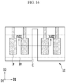
- FIG. 16 illustrates an exemplary embodiment of a region R2 of FIG. 14 .
- FIG. 17 illustrates an exemplary embodiment of a cross-section along a line XVII-XVII' of FIG. 15 .
- FIG. 18 illustrates an exemplary embodiment of a cross-section along a line XVIII-XVIII' of FIG. 16 .
- the display device may include the display panel 10 and the flexible printed circuit film 50 connected to the display panel 10.
- the display panel 10 may include the display area (DA) in which pixels PX are positioned, and the non-display area (NA) adjacent to the display area (DA).
- the non-display area (NA) may include the bending area (BA), the fan out area (FOA), and the pad area (PA).
- the display panel 10 may be bent with respect to the bending axis (X), which may be substantially parallel with the first direction D1 in the bending area (BA).
- the integrated circuit chip 500 may be disposed on the flexible printed circuit film 50.
- the integrated circuit chips 500 may be disposed in the non-display area (NA) of the display panel 10, for example, between the pad area (PA) and the bending area (BA).
- the pad portions (PP) may be positioned along the first direction D1 in the pad area (PA) on the edge of the display panel 10.
- the pad portions (PP) may include pads (P) disposed at a predetermined interval along the first direction D1.
- a plurality of flexible printed circuit films 50 may be connected to the display panel 10.
- Each of the flexible printed circuit films 50 may include a pad portion (PP).
- the display panel according to one or more exemplary embodiments of the present invention may be a relatively small display panel.
- a plurality of pad portions (PP) may be disposed in the pad area (PA), and a single flexible printed circuit film 50 may disposed on each of the pad portions.
- the cutouts (C) may be formed between adjacent pads (P).
- the cutouts (C) may be formed in the display panel 10, and may also be formed in the flexible printed circuit film 50.
- the flexible printed circuit film 50 may be connected to the pad portion (PP) the cutout (C) may penetrate the display panel 10 and the flexible printed circuit film 50.
- FIG. 15 and FIG. 16 show the display panel 10 excluding the flexible printed circuit film 50 in the region R2 of FIG. 14 .
- the cutout (C) may be formed substantially along the second direction D2 from an edge of the pad portion (PP) opposite the display area DA of the display panel 10 toward the display area DA of the display panel 10.
- the cutout (C) may be formed from a point outside the pad portion (PP) opposite the display area DA of the display panel 10 and toward the display area DA of the display panel 10.
- FIG. 17 and FIG. 18 illustrate cross-sections of cutouts (C) in the third direction D3, which may be a thickness direction of the display panel 10.
- the cutouts (C) may be generated in the thickness direction of the display panel 10 from an upper side of the display panel 10 to a predetermined depth.
- the cutout (C) may penetrate the substrate 110 and the adhesive layer 30 from the insulating layers 140 and 160 of the substrate 110 to reach part of the protection film 300.
- the cutout (C) may fully penetrate the display panel 10 from the upper side of the display panel 10 to the protection film 300.
- the pad area (PA) may be thinner than the display area (DA), and thus the pad portion (PP) may be exposed. Thus, the pad area (PA) may have relatively low stiffness, which may result in waviness of the pad area.
- the cutout (C) may reduce or eliminate stress applied to the pad area (PA), which may reduce or eliminate a generation of waviness.
Landscapes
- Physics & Mathematics (AREA)
- Engineering & Computer Science (AREA)
- Nonlinear Science (AREA)
- General Physics & Mathematics (AREA)
- Optics & Photonics (AREA)
- Mathematical Physics (AREA)
- Chemical & Material Sciences (AREA)
- Crystallography & Structural Chemistry (AREA)
- Computer Hardware Design (AREA)
- Theoretical Computer Science (AREA)
- Microelectronics & Electronic Packaging (AREA)
- General Engineering & Computer Science (AREA)
- Human Computer Interaction (AREA)
- Devices For Indicating Variable Information By Combining Individual Elements (AREA)
- Electroluminescent Light Sources (AREA)
- Manufacturing & Machinery (AREA)
- Liquid Crystal (AREA)
Abstract
Description
- This application claims priority under 35 U.S.C. §119 to Korean Patent Application No.
10-2016-0080852 - Exemplary embodiments of the present invention relate to a display device, and more particularly to a bendable display device.
- Display devices such as an organic light emitting device and a liquid crystal display may be manufactured by generating a plurality of layers and elements on a substrate. The substrate of the display device may include glass. A glass substrate may be relatively rigid, relatively heavy and may break. Display devices may include a relatively flexible substrate that is relatively light, relatively strong against impacts, and may be relatively easily deformed.
- A display device including a flexible substrate may be manufactured to bend at an edge where a pad portion to which a flexible printed circuit film (FPC) for transmitting signals is positioned, thus creating a relatively small dead space. When the dead space is reduced, a bezel width of the display device may be reduced and usage of an inner space of the display device may be increased, and thus the display device may be relatively small.
- One or more exemplary embodiments of the present invention provide a display device including a flexible substrate having increased reliability of a bending area and a pad area.
- An exemplary embodiment of the present invention provides a display device including a bendable display panel including a substrate and a plurality of pad portions on the substrate. The substrate includes a cutout between adjacent pad portions of the plurality of pad portions.
- The cutout may be dimensioned and positioned to at least partially isolate movement of a first pad portion from movement of a second pad portion when the bendable display panel is bent.
- The display panel may include a display area displaying an image and a non-display area adjacent to the display area. The plurality of pad portions may be arranged along a first direction in the non-display area, and the cutout may extend in a second direction crossing the first direction.
- The cutout may extend in the second direction from an edge of the display panel opposite the display area of the display panel.
- The display panel may include a bending area between the display area and the pad portions, and the bending area may be bendable with respect to a bending axis extending in the first direction.
- The bending area may include a plurality of wires, and the plurality of wires may extend along the second direction.
- The display panel may include a plurality of fan-outs between the pad portions and the bending area, and the cutout may extend to a region between neighboring fan-outs.
- The display device may include at least one flexible printed circuit film disposed on the pad portions. An integrated circuit chip may be disposed on the flexible printed circuit film.
- The cutout may penetrate the display panel in a thickness direction of the display panel.
- An exemplary embodiment of the present invention provides a display device including a display panel including a display area displaying an image and a non-display area including a plurality of pad portions. At least one flexible printed circuit film is disposed on each of the plurality of pad portions. The pad portions are arranged along a first direction. The display panel includes a cutout between adjacent pad portions of the plurality of pad portions. The cutout extends in a second direction crossing the first direction.
- The display panel may include a bending area between the display area and the pad portions, and the bending area may include a plurality of wires extending along the second direction.
- The bending area may be bendable with respect to a bending axis extending in the first direction.
- A flexible printed circuit film may be disposed on each of the pad portions. A driving circuit chip may be disposed on each of the flexible printed circuit films.
- The cutout may extend in the second direction from an edge of the display panel opposite the display area of the display panel.
- The display panel may include a plurality of fan-outs between the pad portions and the bending area, and the cutout may extend to a region between neighboring fan-outs.
- A plane shape of an end portion of the cutout facing the display area of the display panel may be pointed, may be polygonal or may be round.
- The cutout may penetrate the display panel in a thickness direction of the display panel.
- An exemplary embodiment of the present invention provides a display device including a display panel including a display area displaying an image and a non-display area including a pad portion. A flexible printed circuit film is disposed on the pad portion. The pad portion includes a plurality of pads arranged along a first direction. The display panel includes a cutout formed between adjacent pads and extending in a second direction crossing the first direction.
- The display panel may include a bending area between the display area and the pad portion, and the bending area may include a plurality of wires extending along the second direction.
- The bending area may be bendable with respect to a bending axis extending in the first direction.
- The cutout may be formed along the second direction from an edge of the display panel opposite the display area of the display panel.
- The cutout may be formed in the second direction and may extend beyond the edge of the display panel by a predetermined distance in the pad portion.
- The cutout may penetrate the display panel in a thickness direction of the display panel.
- The cutout may be formed along a thickness direction of the display panel from a top surface of the display panel to a depth above a bottom surface of the display panel.
- The display panel may include a substrate. The pad portion may be positioned on a first side of the substrate, and a protection film may be positioned on a second side of the substrate. The cutout may penetrate the substrate and may be formed through part of the protection film.
- According to an exemplary embodiment of the present invention, application of a force to the wires in the bending area in a direction different from a bending direction may be controlled, and generation of cracks of the wires in the bending area may be reduced or prevented. A generation of waviness may be reduced or prevented in the pad area of the display panel.
- The above and other features of the inventive concept will become more apparent by describing in detail exemplary embodiments thereof, with reference to the accompanying, in which:
-
FIG. 1 is a top plan view of a display device that is not bent according to an exemplary embodiment of the present invention. -
FIG. 2 is a side view of the display device shown inFIG. 1 that is bent. -
FIG. 3 illustrates a comparative example of a region R1 ofFIG. 1 . -
FIG. 4 illustrates an exemplary embodiment of a region R1 ofFIG. 1 . -
FIG. 5 ,FIG. 6 ,FIG. 7 ,FIG. 8 , andFIG. 9 each respectively illustrates an exemplary embodiment of a region R1 ofFIG. 1 . -
FIG. 10 illustrates s an exemplary embodiment of a cross-section with respect to a line X-X' inFIG. 1 . -
FIG. 11 illustrates an exemplary embodiment of a cross-section with respect to a line XI-XI' inFIG. 1 . -
FIG. 12 illustrates an exemplary embodiment of a cross-section of a pixel area inFIG. 1 . -
FIG. 13 illustrates an exemplary embodiment of a cross-section of a pixel area inFIG. 1 . -
FIG. 14 is a top plan view of a display device that is not bent according to an exemplary embodiment of the present invention. -
FIG. 15 illustrates an exemplary embodiment of a region R2 ofFIG. 14 . -
FIG. 16 illustrates an exemplary embodiment of a region R2 ofFIG. 14 . -
FIG. 17 illustrates an exemplary embodiment of a cross-section along a line XVII-XVII' ofFIG. 15 . -
FIG. 18 illustrates an exemplary embodiment of a cross-section along a line XVIII-XVIII' ofFIG. 16 . - Exemplary embodiments of the present invention will be described in more detail below with reference to the accompanying drawings, in which exemplary embodiments of the preset invention are shown. As those skilled in the art would realize, the described embodiments may be modified in various different ways, all without departing from the spirit or scope of the present invention.
- In the drawings, the thicknesses of layers, films, panels, or regions may be exaggerated for clarity. Like reference numerals may refer to like elements throughout the specification and drawings. It will be understood that when an element such as a layer, film, region, or substrate is referred to as being "on" another element, it may be directly on the other element or intervening elements may be present.
- It will be understood that when an element such as a layer, film, region, or substrate is referred to as being "on" another element, it may be directly on the other element or intervening elements may also be present.
- A display device according to an exemplary embodiment of the present invention will be described in more detail below with reference to accompanying drawings.
-
FIG. 1 is a top plan view of a display device that is not bent according to an exemplary embodiment of the present invention.FIG. 2 is a side view of the display device shown inFIG. 1 that is bent. - Referring to
FIG. 1 , the display device may include adisplay panel 10 and at least one flexible printedcircuit film 50 connected to thedisplay panel 10. - The
display panel 10 may include a display area (DA) displaying an image, and a non-display area (NA) in which elements and/or wires (W) generating various signals applied to the display area (DA) and/or transmitting the various signals are disposed. The non-display area may be adjacent to the display area (DA). - As an example, pixels PX may be arranged in a matrix in the display area (DA) of the
display panel 10. In the display area (DA), signal lines including gate lines and data lines may be disposed. The gate lines may extend in a first direction D1 (e.g., a row direction), and the data lines may extend in a second direction D2 (e.g., a column direction) crossing the first direction D1. Alternatively, the gate lines may extend in the same direction as the data lines, for example, in the second direction D2. - At least one gate line and at least one data line may be connected to each of the pixels PX. Each pixel PX may receive a gate signal and a data signal from the signal lines. Regarding the organic light emitting device, driving voltage lines may extend, for example, in the second direction D2 and may transmit a driving voltage to the pixel PX. The driving voltage lines may be positioned in the display area (DA).
- The non-display area (NA) of the
display panel 10 may include a pad area (PA) including pad portions (PP) receiving signals from outside of thedisplay panel 10. Each of the pad portions (PP) may include pads arranged, for example, in the first direction D1 at a predetermined interval. The pad portions (PP) may be disposed on an edge of thedisplay panel 10 along the first direction D1 at a predetermined interval. A cutout (C) may be formed between the neighboring pad portions (PP). As an example, before thedisplay panel 10 is bent, the cutouts (C) may be formed in the second direction D2 toward the display area (DA) from the edge of thedisplay panel 10. However, a formation direction of the cutout (C) is not limited to the second direction D2, and the cutout (C) may be formed in a direction that is oblique to the second direction D2. The cutout (C) may fully penetrate thedisplay panel 10 in a third direction D3 that is a thickness direction of thedisplay panel 10. - Regarding the pad area (PA) of the
display panel 10, neighboring pad portions (PP) may be partially separated from each other along the first direction D1 by the cutouts (C). Thus, when a pad portion of the pad portions (PP) is bent, it might not affect a neighboring pad portion (PP). Thus, stress applied to an area near a pad portion of the pad portions (PP) may be reduced or eliminated. For example, stress on wires (W) positioned in a bending area (BA) of thedisplay panel 10 may be reduced or eliminated and thus an occurrence of cracks in the wires (W) may be reduced or eliminated. - As an example, the cutouts (C) may be formed by cutting the
display panel 10 by use of laser beams or a knife, or by etching thedisplay panel 10 through a photolithography process. - A first end of the flexible printed
circuit film 50 may be connected to each pad portion (PP). An anisotropic conductive film may be disposed between the pad portions (PP) and the flexible printedcircuit film 50. As an example, the flexible printedcircuit film 50 may include a second end connected to a printed circuit board and transmitting signals such as control signals or image data. - A driving device generating and/or processing various signals for driving the
display panel 10 may be positioned in the non-display area (NA) of the display panel 10 (e.g., on the flexible printed circuit film 50). The driving device may be disposed on the printed circuit board. The driving device may include a data driver applying a data signal to the data line, a gate driver applying a gate signal to the gate line, and a signal controller controlling the data driver and the gate driver. - The data driver may be an integrated circuit chip of a plurality of
integrated circuit chips 500 disposed on the flexible printedcircuit film 50. Each of theintegrated circuit chips 500 may be connected as a tape carrier package to a pad portion of the pad portions (PP). The data driver may be positioned between the display area (DA) and the pad area (PA). The gate driver may be positioned in the non-display area (NA) on edges of the display panel 10 (e.g., on left/right sides of thedisplay panel 10 along the first direction). As an example, the gate driver may be an integrated circuit chip of the integrated circuit chips 500. The signal controller may be an integrated circuit chip ofintegrated circuit chips 500 and may be connected to the printed circuit board. The signal controller may transmit control signals through the flexible printedcircuit film 50. - The
display panel 10 includes the bending area (BA) between the display area (DA) and the pad area (PA). The bending area (BA) may an area extending along thedisplay panel 10 in the first direction D1. Thedisplay panel 10 may be bent along a bending axis (X), which is substantially parallel with the first direction D1. As an example, the flexible printedcircuit films 50 may be positioned behind the display area (DA) when thedisplay panel 10 is bent. According to an exemplary embodiment of the present invention, the bending area (BA) may be in the display area (DA) and the non-display area (NA); however exemplary embodiments of the present invention are not limited thereto. For example, the bending area (BA) may be entirely in the non-display area (NA). - A fan out area (FOA) may be between the bending area (BA) and the pad area (PA). The fan out area (FOA) may be positioned along the first direction D1. The fan out area (FOA) may include a plurality of fan-outs (FO). Wires (W) connected to the pads of the pad portions (PP) may be adjacent to the fan-outs (FO). The fan-outs (FO) may be positioned at a predetermined interval along the first direction D1. A separation between adjacent fan-outs (FO) may become gradually narrower along the second direction from the pad portions (PP) toward the display area (DA) of the
display panel 10. The wires (W) may pass through the fan-out area (FOA) and the bending area (BA) and may be connected to various signal lines such as data lines. When thedisplay panel 10 is not bent, the wires (W) may extend in the second direction D2 in the bending area (BA) and may be substantially perpendicular to the bending axis (X). The cutouts (C) positioned in the pad area (PA) may extend to a region between adjacent fan-outs (FO) of the fan out area (FOA). Thus, stress applied in the fan out area (FOA) when thedisplay panel 10 is bent may be reduced or eliminated. The wires (W) are not positioned in the region in which the cutouts (C) are formed. - The cutouts (C) according to an exemplary embodiment of the present invention will be described in more detail below with reference to
FIG. 3 andFIG. 4 . -
FIG. 3 illustrates a comparative example of a region R1 ofFIG. 1 .FIG. 4 illustrates an exemplary embodiment of the region R1 ofFIG. 1 . - Referring to
FIG. 3 , a case in which a cutout is not formed between adjacent pad portions (PP) is illustrated. A flexible printedcircuit film 50 on which anintegrated circuit chip 500 is disposed may be connected to each pad portion (PP). During a process for transferring or bending the display device, a region near the pad portion (PP) may be folded in an undesired manner because of weight of theintegrated circuit chip 500, and thus the folded region may be relatively wide. For example, when the region near a pad portion of the pad portions (PP) is folded, an adjacent pad portion of the pad portions (PP) may also be folded in a folding direction (DF). The folding direction (DF) may cross a bending direction (DB) of the bending area (BA). The wires (W) (e.g., asecond wire portion 179 illustrated, for example, inFIG. 10 ) in the bending area (BA) may be configured to well withstand a stress in the bending direction (DB), but not in another direction than the bending direction (DB), and thus when stress is applied in the folding direction (DF) traversing the bending direction (DB), for example, the stress may cause the wires (W) to crack or short-circuit. Additionally, a relatively wide folding region may result in a plurality of wires (W) being damaged. - Referring to
FIG. 4 , the cutout (C) may be formed between neighboring pad portions (PP). The flexible printedcircuit film 50 on which theintegrated circuit chip 500 is disposed may be connected to a corresponding pad portion (PP), and the region near the pad portion (PP) to which the flexible printedcircuit film 50 is bonded may be undesirably folded by the weight of theintegrated circuit chip 500. However, according to an exemplary embodiment of the present invention, when the region near a pad portion of the pad portions (PP) is folded, such folding does not extend to adjacent pad portions (PP) but is blocked by the cutout (C). Thus, the folding may be limited to the region corresponding to one pad portion (PP), and the folding direction (DF) may substantially correspond to the bending direction (DB) of the bending area (BA). When the folding direction (DF) substantially corresponds to the bending direction (DB), the cracking of the wires (W) may be reduced or eliminated. The cutout (C) may extend to a space between the fan-outs (FO) of the fan out area (FOA) from the edge of thedisplay panel 10 thus further reducing an influence of folding a first pad portion on adjacent pad portions (PP). - The cutout (C) may have a V shape (or a plane shape of a triangle) that becomes narrower and pointed at an end of the V shaped cutout closer to the display area DA of the display panel; however exemplary embodiments of the present invention are not limited thereto. The cutout (C) according to some exemplary embodiments of the present invention will be described in more detail below with reference to
FIG. 5 to FIG. 9 . -
FIG. 5 ,FIG. 6 ,FIG. 7 ,FIG. 8 , andFIG. 9 each respectively illustrates an exemplary embodiment of a region R1 ofFIG. 1 . - Referring to
FIG. 5 , the cutout (C) may have a plane shape of a rectangle with a substantially constant width. Referring toFIG. 6 , the cutout (C) may have a substantially rectangular shape in which an end of the cutout (C) closest to the display area DA of the display panel is rounded. Referring toFIG. 7 andFIG. 8 , the cutout (C) may have a plane shape of a semicircle or may have a plane shape of a semi-ellipse. Referring toFIG. 9 , the cutout (C) may have a plane shape of a light bulb. According to some exemplary embodiments of the present invention, the cutout (C) may have various shapes between the neighboring pad portions (PP), and the cutout (C) reduces or prevents the folding influence of a pad portion of the pad portions (PP) from being applied to adjacent pad portions (PP). Thus damage to the wires (W) in the bending area (BA) may be reduced or eliminated. Cutouts (C) may be formed between each pair of adjacent pad portions (PP), or cutouts (C) between some pad portions (PP) may be omitted. - A stacked configuration of the display device according to some exemplary embodiments of the present invention will be described below in more detail with reference to the pixel PX of the non-display area (NA) and the display area (DA) in which the bending area (BA) and the pad area (PA) are provided.
-
FIG. 10 illustrates an exemplary embodiment of a cross-section with respect to a line X-X' inFIG. 1 .FIG. 11 illustrates an exemplary embodiment of a cross-section with respect to a line XI-XI' inFIG. 1 .FIG. 12 illustrates an exemplary embodiment of a cross-section of a pixel area inFIG. 1 .FIG. 13 illustrates another exemplary embodiment of a cross-section of a pixel area inFIG. 1 . -
FIG. 12 exemplifies a case in which the display device is an organic light emitting device, andFIG. 13 exemplifies a case in which the display device is a liquid crystal display. Configurations ofFIG. 10 andFIG. 11 may be applied to display devices according to other exemplary embodiments of the present invention, regardless of the type of the display device. An organic light emitting device according to an exemplary embodiment of the present invention will be described below in more detail with reference toFIG. 10 ,FIG. 11 , andFIG. 12 . Technical features that are the same as those described above may be omitted, and thus duplicative descriptions may be omitted. - Referring to
FIG. 10 ,FIG. 11 , andFIG. 12 , thedisplay panel 10 may include asubstrate 110 and a plurality of layers disposed on thesubstrate 110. - The
substrate 110 may be a flexible substrate including a transparent polymer film. For example, thesubstrate 110 may include a plastic such as polyimide, polyamide, or polyethylene terephthalate. - The
substrate 110 may include a buffer layer. The buffer layer may reduce or prevent a penetration of impurities or moisture into thesubstrate 110. The buffer layer may be formed on substantially theentire substrate 110, except for in the bending area (BA). - A
semiconductor 131 of a transistor (TR) may be disposed on thesubstrate 110. Agate insulating layer 140 may be disposed on thesemiconductor 131. Thesemiconductor 131 may include a source region, a drain region, and a channel region between the source and drain regions. Thesemiconductor 131 may include polysilicon, an oxide semiconductor, or amorphous silicon. Thegate insulating layer 140 may be formed by stacking inorganic insulating materials such as a silicon oxide or a silicon nitride. Thegate insulating layer 140 need not be provided in the bending area (BA). According to an exemplary embodiment of the present invention, thegate insulating layer 140 may be positioned in a region overlapping afirst pad layer 127 or a gate conductor such as agate electrode 124, and it need not be positioned in the pad area (PA). - The
first pad layer 127 of a pad (P), afirst wire portion 129 of the wire (W), and a gate conductor including thegate electrode 124 of the transistor (TR) may be positioned on thegate insulating layer 140. Thefirst pad layer 127, thefirst wire portion 129, and thegate electrode 124 may be formed by stacking one or more conductive materials such as copper (Cu), aluminum (Al), silver (Ag), molybdenum (Mo), chromium (Cr), tantalum (Ta), or titanium (Ti) on thesubstrate 110 and patterning the one or more stacked conductive materials. - An interlayer insulating
layer 160 may be disposed on thefirst pad layer 127, thefirst wire portion 129, and thegate electrode 124. The interlayer insulatinglayer 160 may include an inorganic material. The interlayer insulatinglayer 160 need not be positioned in the bending area (BA). - A
second pad layer 177 of the pad (P), asecond wire portion 179 of the wire (W), and a data conductor including asource electrode 173 and adrain electrode 175 of the transistor (TR) may be disposed on theinterlayer insulating layer 160. Thesecond pad layer 177 may overlap thefirst pad layer 127 and may be connected to thefirst pad layer 127 through a contact hole formed in theinterlayer insulating layer 160. Thesecond wire portion 179 may cross the bending area (BA) and may extend beyond the bending area (BA). Thesecond wire portion 179 may be connected to an extension of thefirst pad layer 127 through first contact holes formed in theinterlayer insulating layer 160 and may be connected to thefirst wire portion 129 through second contact holes formed in theinterlayer insulating layer 160. Thesource electrode 173 and thedrain electrode 175 may be connected to the source region and the drain region of thesemiconductor 131, respectively, through contact holes formed in theinterlayer insulating layer 160 and thegate insulating layer 140. As an example, the data conductor may include a metal such as copper (Cu), aluminum (Al), silver (Ag), molybdenum (Mo), chromium (Cr), gold (Au), platinum (Pt), palladium (Pd), tantalum (Ta), tungsten (W), titanium (Ti), or nickel (Ni), or a metal alloy thereof. For example, the data conductor may include aluminum with a relatively low Young's modulus or an aluminum-based metal such as an aluminum alloy. Thesecond pad layer 177 and thesecond wire portion 179 may be formed of the same material forming the data conductor. Thus, thesecond wire portion 179 of the wire (W) positioned in the bending area (BA) may experience a relatively low amount of stress during bending of the display panel, and thus an occurrence of a short-circuit during or after bending of the display panel may be reduced or eliminated. - In the bending area (BA), a
protective layer 165 may be positioned between thesubstrate 110 and thesecond wire portion 179. Theprotective layer 165 may include an organic material. - A
passivation layer 180 may be disposed on thesecond wire portion 179, thesource electrode 173, and thedrain electrode 175. Thepassivation layer 180 may include an organic material. In the bending area (BA), thesecond wire portion 179 may be positioned between theprotective layer 165 and thepassivation layer 180. Thus, damage to thesecond wire portion 179 may be reduced or prevented by theprotective layer 165 and thepassivation layer 180 when is thesecond wire portion 179 is bent. Thepassivation layer 180 need not be positioned in the pad area (PA), or thepassivation layer 180 may be positioned between the adjacent pads (P). - A
pixel electrode 191 may be disposed on thepassivation layer 180. Thepixel electrode 191 may be connected to thedrain electrode 175 through the contact hole formed in thepassivation layer 180 and may receive a data signal. - A
pixel definition layer 360 may be disposed on thepassivation layer 180 and on at least a part of thepixel electrode 191. Thepixel definition layer 360 may include an opening overlapping thepixel electrode 191. In the opening of thepixel definition layer 360, anemission layer 370 may be disposed on thepixel electrode 191, and acommon electrode 270 may be disposed on theemission layer 370. Thepixel electrode 191, theemission layer 370, and thecommon electrode 270 may form an organic light emitting diode. Thepixel electrode 191 may be an anode of the organic light emitting diode, and thecommon electrode 270 may be a cathode of the organic light emitting diode. Thecommon electrode 270 may include a transparent conductive material such as an indium tin oxide (ITO) or an indium zinc oxide (IZO). Anencapsulation layer 390 protecting the organic light emitting diode may be disposed on thecommon electrode 270. Theencapsulation layer 390 may include at least one organic material layer and/or at least one inorganic material layer. - The
pixel definition layer 360 and theencapsulation layer 390 might not be positioned on the pad portion (PP), thus exposing the pad (P). Thepixel definition layer 360 may be provided in the bending area (BA), and theencapsulation layer 390 need not be provided therein. In the bending area (BA), a bending protection layer releasing and protecting against tensile stress of thesecond portion 179 of the wire (W) may be positioned on thepixel definition layer 360. - The flexible printed
circuit film 50 including bumps (B) may be positioned on the pad portion (PP). An anisotropic conductive film including conductive particles may be positioned between the pad (P) and the flexible printedcircuit film 50. The anisotropic conductive film may bond the flexible printedcircuit film 50 to the pad portion (PP) and electrically connect the pad (P) and the bump (B). - A
protection film 300 may be positioned below thesubstrate 110. Theprotection film 300 may be attached to thesubstrate 110 by anadhesive layer 30 such as a pressure sensitive adhesive (PSA) or an optically clear adhesive (OCA). Theprotection film 300 may be a polymer film, and it may include a plastic such as polyethylene terephthalate, polyethylene naphthalate, polyethylene sulfide, polyethylene, or polyimide. Theprotection film 300 need not be positioned in the bending area (BA), which may reduce a bending stress of the bending area (BA). - Referring to
FIG. 11 , the cutout (C) may be formed between adjacent pad portions (PP). Each of the cutouts (C) may penetrate thedisplay panel 10 in a third direction D3. The third direction D3 may be a thickness direction of thedisplay panel 10. Thus, the cutouts (C) may be formed in thesubstrate 110, the insulatinglayers protection film 300. - Referring to
FIG. 13 , thegate electrode 124 of the transistor (TR) may be disposed on thesubstrate 110, and thegate insulating layer 140 may be disposed on thegate electrode 124. Asemiconductor 154 may be disposed on thegate insulating layer 140, and thesource electrode 173 and thedrain electrode 175 of the transistor (TR) may be disposed on thesemiconductor 154. - The
passivation layer 180 may be disposed on thesource electrode 173 and thedrain electrode 175, and thepixel electrode 191 may be disposed on thepassivation layer 180. Thepixel electrode 191 may be connected to thedrain electrode 175 through the contact hole formed in thepassivation layer 180 and may receive a data signal. - A
liquid crystal layer 3 including liquid crystal molecules 31 may be disposed on thepixel electrode 191, and an insulatinglayer 210 sealing theliquid crystal layer 3 may be positioned on theliquid crystal layer 3. The insulatinglayer 210 may have substantially a same shape as a shape of thesubstrate 110. - The
common electrode 270 may provide an electric field to theliquid crystal layer 3 together with thepixel electrode 191. Thecommon electrode 270 and thepixel electrode 191 may control a directional orientation of the liquid crystal molecules 31. An alignment layer may be positioned between thepixel electrode 191 and theliquid crystal layer 3 and between theliquid crystal layer 3 and thecommon electrode 270. - According to an exemplary embodiment of the present invention, the
common electrode 270 may be positioned between thesubstrate 110 and theliquid crystal layer 3. - A display device according to a further exemplary embodiment of the present invention will be described in more detail below with reference to
FIG. 14 to FIG. 18 . The same constituent elements or features as in the above-described exemplary embodiments might not be described again, and thus redundant descriptions may be omitted. -
FIG. 14 is a top plan view of a display device that is not bent according to an exemplary embodiment of the present invention.FIG. 15 illustrates an exemplary embodiment of a region R2 ofFIG. 14 .FIG. 16 illustrates an exemplary embodiment of a region R2 ofFIG. 14 .FIG. 17 illustrates an exemplary embodiment of a cross-section along a line XVII-XVII' ofFIG. 15 .FIG. 18 illustrates an exemplary embodiment of a cross-section along a line XVIII-XVIII' ofFIG. 16 . - Referring to
FIG. 14 , the display device may include thedisplay panel 10 and the flexible printedcircuit film 50 connected to thedisplay panel 10. - The
display panel 10 may include the display area (DA) in which pixels PX are positioned, and the non-display area (NA) adjacent to the display area (DA). The non-display area (NA) may include the bending area (BA), the fan out area (FOA), and the pad area (PA). Thedisplay panel 10 may be bent with respect to the bending axis (X), which may be substantially parallel with the first direction D1 in the bending area (BA). Theintegrated circuit chip 500 may be disposed on the flexible printedcircuit film 50. Theintegrated circuit chips 500 may be disposed in the non-display area (NA) of thedisplay panel 10, for example, between the pad area (PA) and the bending area (BA). - The pad portions (PP) may be positioned along the first direction D1 in the pad area (PA) on the edge of the
display panel 10. The pad portions (PP) may include pads (P) disposed at a predetermined interval along the first direction D1. In an exemplary embodiment of the present invention, a plurality of flexible printedcircuit films 50 may be connected to thedisplay panel 10. Each of the flexible printedcircuit films 50 may include a pad portion (PP). The display panel according to one or more exemplary embodiments of the present invention may be a relatively small display panel. According to an exemplary embodiment of the present invention, a plurality of pad portions (PP) may be disposed in the pad area (PA), and a single flexible printedcircuit film 50 may disposed on each of the pad portions. - The cutouts (C) may be formed between adjacent pads (P). The cutouts (C) may be formed in the
display panel 10, and may also be formed in the flexible printedcircuit film 50. For example, the flexible printedcircuit film 50 may be connected to the pad portion (PP) the cutout (C) may penetrate thedisplay panel 10 and the flexible printedcircuit film 50. -
FIG. 15 andFIG. 16 show thedisplay panel 10 excluding the flexible printedcircuit film 50 in the region R2 ofFIG. 14 . Referring toFIG. 15 , the cutout (C) may be formed substantially along the second direction D2 from an edge of the pad portion (PP) opposite the display area DA of thedisplay panel 10 toward the display area DA of thedisplay panel 10. Referring toFIG. 16 , the cutout (C) may be formed from a point outside the pad portion (PP) opposite the display area DA of thedisplay panel 10 and toward the display area DA of thedisplay panel 10. -
FIG. 17 andFIG. 18 illustrate cross-sections of cutouts (C) in the third direction D3, which may be a thickness direction of thedisplay panel 10. The cutouts (C) may be generated in the thickness direction of thedisplay panel 10 from an upper side of thedisplay panel 10 to a predetermined depth. For example, referring toFIG. 17 , the cutout (C) may penetrate thesubstrate 110 and theadhesive layer 30 from the insulatinglayers substrate 110 to reach part of theprotection film 300. Referring toFIG. 18 , the cutout (C) may fully penetrate thedisplay panel 10 from the upper side of thedisplay panel 10 to theprotection film 300. - The pad area (PA) may be thinner than the display area (DA), and thus the pad portion (PP) may be exposed. Thus, the pad area (PA) may have relatively low stiffness, which may result in waviness of the pad area. When the cutout (C) is generated in the pad area (PA) according to an exemplary embodiment of the present invention, the cutout (C) may reduce or eliminate stress applied to the pad area (PA), which may reduce or eliminate a generation of waviness.
- While the present invention has been shown and described with reference to the exemplary embodiments thereof, it will be apparent to those of ordinary skill in the art that various changes in form and detail may be made thereto without departing from the scope of the present invention.
Claims (12)
- A display device comprising:a bendable display panel (10) including a substrate (110) and a plurality of pad portions (PP) on the substrate (110),wherein the substrate (110) includes a cutout (C) between adjacent pad portions (PP) of the plurality of pad portions (PP).
- The display device of claim 1, wherein
the display panel (10) includes a display area (DA) for displaying an image and a non-display area (NA) adjacent to the display area (DA),
the plurality of pad portions (PP) are arranged along a first direction (D1) in the non-display area (NA), and
the cutout (C) extends in a second direction (D2) crossing the first direction (D1). - The display device of claim 2, wherein
the cutout (C) extends in the second direction (D2) from an edge of the non -display rea (NA) of the display panel (10) towards the display area (DA) of the display panel (10). - The display device of one of claims 2 and 3, wherein
the display panel (10) includes a bending area (BA) between the display area (DA) and the pad portions (PP), and
the bending area (BA) is bendable with respect to a bending axis (X) extending in the first direction (D1). - The display device of claim 4, wherein
the bending area (BA) includes a plurality of wires (W), and
the plurality of wires (W) extend along the second direction (D2). - The display device of one of claims 4 and 5, wherein
the display panel (10) includes a plurality of fan-outs (FO) between the pad portions (PP) and the bending area (BA), and
the cutout (C) extends to a region between neighboring fan-outs (FO). - The display device of one of the preceding claims, further comprising:at least one flexible printed circuit film (50) disposed on each of the pad portions (PP).
- The display device of claim 7, further comprising:an integrated circuit chip (500) disposed on each of the flexible printed circuit films (50).
- The display device of one of the preceding claims, wherein
the cutout (C) penetrates the display panel (10) in a thickness direction (D3) of the display panel (10). - The display device of one of claims 1-8, wherein
the cutout (C) is formed along a thickness direction (D3) of the display panel (10) from a top surface of the display panel to a depth above a bottom surface of the display panel. - The display device of claim 10, further comprising
a protection film (300) attached to a surface of the substrate (110) opposite to the surface on which the pad portions (PP) are formed,
wherein the cutout (C) extends through the substrate (110) and a part of the protection film (300) in a thickness direction (D3) of the display panel (10). - The display device of one of the preceding claims, wherein
a plane shape of an end portion of the cutout (C) facing the display area (DA) of the display panel (10) is pointed, polygonal, or round.
Applications Claiming Priority (1)
| Application Number | Priority Date | Filing Date | Title |
|---|---|---|---|
| KR1020160080852A KR102659601B1 (en) | 2016-06-28 | 2016-06-28 | Display device |
Publications (2)
| Publication Number | Publication Date |
|---|---|
| EP3264465A1 true EP3264465A1 (en) | 2018-01-03 |
| EP3264465B1 EP3264465B1 (en) | 2021-01-06 |
Family
ID=59315385
Family Applications (1)
| Application Number | Title | Priority Date | Filing Date |
|---|---|---|---|
| EP17178277.4A Active EP3264465B1 (en) | 2016-06-28 | 2017-06-28 | Bendable display device |
Country Status (5)
| Country | Link |
|---|---|
| US (1) | US10719103B2 (en) |
| EP (1) | EP3264465B1 (en) |
| KR (1) | KR102659601B1 (en) |
| CN (1) | CN107544172B (en) |
| TW (1) | TWI747916B (en) |
Families Citing this family (28)
| Publication number | Priority date | Publication date | Assignee | Title |
|---|---|---|---|---|
| US11031573B2 (en) * | 2017-11-30 | 2021-06-08 | Wuhan China Star Optoelectronics Semiconductor Display Technology Co., Ltd. | Encapsulation layer of flexible display panel and flexible display |
| KR102403929B1 (en) * | 2018-02-23 | 2022-06-02 | 삼성디스플레이 주식회사 | Display device and method of manufacturing the same |
| KR102529077B1 (en) * | 2018-03-06 | 2023-05-09 | 삼성디스플레이 주식회사 | Display device |
| CN108304097B (en) * | 2018-04-13 | 2021-04-23 | 业成科技(成都)有限公司 | Curved touch module structure and bonding method thereof |
| CN108598142B (en) * | 2018-06-28 | 2020-11-17 | 上海天马微电子有限公司 | Flexible display substrate, flexible display panel and flexible display device |
| KR102497285B1 (en) | 2018-07-03 | 2023-02-08 | 삼성디스플레이 주식회사 | Display apparatus comprising display unit including an indented shape |
| KR102649145B1 (en) * | 2018-09-18 | 2024-03-21 | 삼성디스플레이 주식회사 | display device |
| WO2020065989A1 (en) * | 2018-09-28 | 2020-04-02 | シャープ株式会社 | Rollable electronic device |
| KR102598831B1 (en) * | 2018-10-04 | 2023-11-03 | 엘지디스플레이 주식회사 | Stretchable display device |
| CN112638576A (en) * | 2018-12-21 | 2021-04-09 | 深圳市柔宇科技股份有限公司 | Fixing method of metal sheet and flexible display device |
| CN109917593B (en) * | 2019-02-22 | 2022-05-13 | 京东方科技集团股份有限公司 | Display panel, preparation method thereof and display device |
| KR20200108139A (en) * | 2019-03-06 | 2020-09-17 | 삼성디스플레이 주식회사 | Display device and method for manufacturing the same |
| WO2020196745A1 (en) * | 2019-03-27 | 2020-10-01 | パナソニックIpマネジメント株式会社 | Stretchable circuit board |
| CN109950222B (en) * | 2019-03-28 | 2021-08-31 | 京东方科技集团股份有限公司 | A flexible display panel and display device |
| KR102840571B1 (en) * | 2019-05-09 | 2025-07-30 | 삼성디스플레이 주식회사 | Display device |
| US11444120B2 (en) * | 2020-01-14 | 2022-09-13 | Au Optronics Corporation | Display apparatus and method of fabricating the same |
| CN111292620A (en) * | 2020-02-24 | 2020-06-16 | 京东方科技集团股份有限公司 | A display panel, its manufacturing method, and display device |
| KR102783279B1 (en) * | 2020-07-07 | 2025-03-20 | 삼성디스플레이 주식회사 | Display panel and manufacturing method for the same |
| CN114342083B (en) * | 2020-08-10 | 2025-10-10 | 京东方科技集团股份有限公司 | Display substrate and display device |
| JP7503959B2 (en) * | 2020-08-11 | 2024-06-21 | 株式会社ジャパンディスプレイ | Display device |
| KR102922576B1 (en) * | 2020-08-31 | 2026-02-06 | 삼성디스플레이 주식회사 | Display device and manufacturing method for the same |
| KR102722114B1 (en) * | 2020-12-29 | 2024-10-28 | 엘지디스플레이 주식회사 | Display Device |
| KR20230035177A (en) * | 2021-09-03 | 2023-03-13 | 삼성디스플레이 주식회사 | Display device |
| WO2023184162A1 (en) * | 2022-03-29 | 2023-10-05 | 京东方科技集团股份有限公司 | Display module and vehicle-mounted display device |
| JP2023152427A (en) * | 2022-04-04 | 2023-10-17 | 凸版印刷株式会社 | light control sheet |
| CN115394201B (en) * | 2022-08-29 | 2023-11-17 | 京东方科技集团股份有限公司 | Display panel and display device |
| KR20240094242A (en) * | 2022-12-15 | 2024-06-25 | 삼성디스플레이 주식회사 | Circuit board and display device including the same |
| KR20250045524A (en) | 2023-09-25 | 2025-04-02 | 삼성디스플레이 주식회사 | display device |
Citations (3)
| Publication number | Priority date | Publication date | Assignee | Title |
|---|---|---|---|---|
| US20020067456A1 (en) * | 2000-10-26 | 2002-06-06 | Hironobu Tatsumi | Liquid crystal display element |
| US20130161661A1 (en) * | 2011-12-22 | 2013-06-27 | Sony Corporation | Circuit board, display module, and electronic apparatus |
| US20140239277A1 (en) * | 2013-02-25 | 2014-08-28 | Samsung Display Co., Ltd. | Display device |
Family Cites Families (16)
| Publication number | Priority date | Publication date | Assignee | Title |
|---|---|---|---|---|
| US5436745A (en) * | 1994-02-23 | 1995-07-25 | Ois Optical Imaging Systems, Inc. | Flex circuit board for liquid crystal display |
| KR20040062197A (en) | 2002-12-31 | 2004-07-07 | 엘지.필립스 엘시디 주식회사 | Tape carrier package cover structure |
| JP4938239B2 (en) * | 2004-04-23 | 2012-05-23 | シャープ株式会社 | Display device |
| KR20080039699A (en) * | 2006-11-01 | 2008-05-07 | 삼성전자주식회사 | Circuit board and display device including the same |
| JP4360405B2 (en) | 2007-01-05 | 2009-11-11 | エプソンイメージングデバイス株式会社 | Electro-optical device and electronic apparatus |
| CN102243383A (en) * | 2010-05-10 | 2011-11-16 | 瀚宇彩晶股份有限公司 | Fan-out signal line structure and display panel |
| KR101697972B1 (en) * | 2011-08-24 | 2017-01-20 | 엘지디스플레이 주식회사 | Flexible Display Device |
| CN103367947A (en) * | 2012-04-10 | 2013-10-23 | 宸鸿科技(厦门)有限公司 | Connection structure |
| KR102009657B1 (en) | 2012-10-31 | 2019-08-12 | 엘지디스플레이 주식회사 | Flexible display panel and fabricating method thereof, media display terminal |
| KR102117890B1 (en) | 2012-12-28 | 2020-06-02 | 엘지디스플레이 주식회사 | Flexible display device and method for manufacturing the same |
| KR102081650B1 (en) * | 2013-04-10 | 2020-02-26 | 엘지디스플레이 주식회사 | Flexible display device and method of manufacturing the same |
| KR102046426B1 (en) | 2013-07-12 | 2019-12-03 | 삼성디스플레이 주식회사 | Display device and method of manufacturing the same |
| US9196848B2 (en) | 2013-07-12 | 2015-11-24 | Samsung Display Co., Ltd. | Display device and method of manufacturing the same |
| TWI494822B (en) * | 2013-12-06 | 2015-08-01 | Au Optronics Corp | Touch display device with flexible circuit module |
| US10582612B2 (en) * | 2014-06-30 | 2020-03-03 | Lg Display Co., Ltd. | Flexible display device with reduced bend stress wires and manufacturing method for the same |
| CN104464524A (en) * | 2015-01-06 | 2015-03-25 | 京东方科技集团股份有限公司 | Display substrate, display panel and display device |
-
2016
- 2016-06-28 KR KR1020160080852A patent/KR102659601B1/en active Active
-
2017
- 2017-06-07 US US15/616,434 patent/US10719103B2/en active Active
- 2017-06-28 CN CN201710507554.4A patent/CN107544172B/en active Active
- 2017-06-28 TW TW106121673A patent/TWI747916B/en active
- 2017-06-28 EP EP17178277.4A patent/EP3264465B1/en active Active
Patent Citations (3)
| Publication number | Priority date | Publication date | Assignee | Title |
|---|---|---|---|---|
| US20020067456A1 (en) * | 2000-10-26 | 2002-06-06 | Hironobu Tatsumi | Liquid crystal display element |
| US20130161661A1 (en) * | 2011-12-22 | 2013-06-27 | Sony Corporation | Circuit board, display module, and electronic apparatus |
| US20140239277A1 (en) * | 2013-02-25 | 2014-08-28 | Samsung Display Co., Ltd. | Display device |
Also Published As
| Publication number | Publication date |
|---|---|
| EP3264465B1 (en) | 2021-01-06 |
| US20170371376A1 (en) | 2017-12-28 |
| KR20180002108A (en) | 2018-01-08 |
| TWI747916B (en) | 2021-12-01 |
| TW201802782A (en) | 2018-01-16 |
| US10719103B2 (en) | 2020-07-21 |
| CN107544172A (en) | 2018-01-05 |
| CN107544172B (en) | 2022-12-20 |
| KR102659601B1 (en) | 2024-04-22 |
Similar Documents
| Publication | Publication Date | Title |
|---|---|---|
| EP3264465B1 (en) | Bendable display device | |
| KR102529077B1 (en) | Display device | |
| KR102433889B1 (en) | Display device | |
| US10712780B2 (en) | Display device | |
| EP3644372B1 (en) | Display device | |
| US10886326B2 (en) | Display device | |
| US12213374B2 (en) | Display device | |
| US10547025B2 (en) | Display device | |
| CN109994646B (en) | display device | |
| CN107464887A (en) | Flexible display apparatus | |
| CN111668393B (en) | Display device and method of manufacturing the same | |
| US20180011369A1 (en) | Display device having a connection member secured in place by a conductive layer | |
| CN107665873B (en) | Integrated circuit chip and display device including same |
Legal Events
| Date | Code | Title | Description |
|---|---|---|---|
| PUAI | Public reference made under article 153(3) epc to a published international application that has entered the european phase |
Free format text: ORIGINAL CODE: 0009012 |
|
| STAA | Information on the status of an ep patent application or granted ep patent |
Free format text: STATUS: THE APPLICATION HAS BEEN PUBLISHED |
|
| AK | Designated contracting states |
Kind code of ref document: A1 Designated state(s): AL AT BE BG CH CY CZ DE DK EE ES FI FR GB GR HR HU IE IS IT LI LT LU LV MC MK MT NL NO PL PT RO RS SE SI SK SM TR |
|
| AX | Request for extension of the european patent |
Extension state: BA ME |
|
| STAA | Information on the status of an ep patent application or granted ep patent |
Free format text: STATUS: REQUEST FOR EXAMINATION WAS MADE |
|
| 17P | Request for examination filed |
Effective date: 20180601 |
|
| RBV | Designated contracting states (corrected) |
Designated state(s): AL AT BE BG CH CY CZ DE DK EE ES FI FR GB GR HR HU IE IS IT LI LT LU LV MC MK MT NL NO PL PT RO RS SE SI SK SM TR |
|
| STAA | Information on the status of an ep patent application or granted ep patent |
Free format text: STATUS: EXAMINATION IS IN PROGRESS |
|
| 17Q | First examination report despatched |
Effective date: 20191008 |
|
| GRAP | Despatch of communication of intention to grant a patent |
Free format text: ORIGINAL CODE: EPIDOSNIGR1 |
|
| STAA | Information on the status of an ep patent application or granted ep patent |
Free format text: STATUS: GRANT OF PATENT IS INTENDED |
|
| INTG | Intention to grant announced |
Effective date: 20200803 |
|
| GRAS | Grant fee paid |
Free format text: ORIGINAL CODE: EPIDOSNIGR3 |
|
| GRAA | (expected) grant |
Free format text: ORIGINAL CODE: 0009210 |
|
| STAA | Information on the status of an ep patent application or granted ep patent |
Free format text: STATUS: THE PATENT HAS BEEN GRANTED |
|
| AK | Designated contracting states |
Kind code of ref document: B1 Designated state(s): AL AT BE BG CH CY CZ DE DK EE ES FI FR GB GR HR HU IE IS IT LI LT LU LV MC MK MT NL NO PL PT RO RS SE SI SK SM TR |
|
| REG | Reference to a national code |
Ref country code: GB Ref legal event code: FG4D |
|
| REG | Reference to a national code |
Ref country code: AT Ref legal event code: REF Ref document number: 1353296 Country of ref document: AT Kind code of ref document: T Effective date: 20210115 Ref country code: CH Ref legal event code: EP |
|
| REG | Reference to a national code |
Ref country code: DE Ref legal event code: R096 Ref document number: 602017030791 Country of ref document: DE |
|
| REG | Reference to a national code |
Ref country code: IE Ref legal event code: FG4D |
|
| REG | Reference to a national code |
Ref country code: NL Ref legal event code: FP |
|
| REG | Reference to a national code |
Ref country code: AT Ref legal event code: MK05 Ref document number: 1353296 Country of ref document: AT Kind code of ref document: T Effective date: 20210106 |
|
| REG | Reference to a national code |
Ref country code: LT Ref legal event code: MG9D |
|
| PG25 | Lapsed in a contracting state [announced via postgrant information from national office to epo] |
Ref country code: LT Free format text: LAPSE BECAUSE OF FAILURE TO SUBMIT A TRANSLATION OF THE DESCRIPTION OR TO PAY THE FEE WITHIN THE PRESCRIBED TIME-LIMIT Effective date: 20210106 Ref country code: BG Free format text: LAPSE BECAUSE OF FAILURE TO SUBMIT A TRANSLATION OF THE DESCRIPTION OR TO PAY THE FEE WITHIN THE PRESCRIBED TIME-LIMIT Effective date: 20210406 Ref country code: HR Free format text: LAPSE BECAUSE OF FAILURE TO SUBMIT A TRANSLATION OF THE DESCRIPTION OR TO PAY THE FEE WITHIN THE PRESCRIBED TIME-LIMIT Effective date: 20210106 Ref country code: FI Free format text: LAPSE BECAUSE OF FAILURE TO SUBMIT A TRANSLATION OF THE DESCRIPTION OR TO PAY THE FEE WITHIN THE PRESCRIBED TIME-LIMIT Effective date: 20210106 Ref country code: GR Free format text: LAPSE BECAUSE OF FAILURE TO SUBMIT A TRANSLATION OF THE DESCRIPTION OR TO PAY THE FEE WITHIN THE PRESCRIBED TIME-LIMIT Effective date: 20210407 Ref country code: NO Free format text: LAPSE BECAUSE OF FAILURE TO SUBMIT A TRANSLATION OF THE DESCRIPTION OR TO PAY THE FEE WITHIN THE PRESCRIBED TIME-LIMIT Effective date: 20210406 Ref country code: PT Free format text: LAPSE BECAUSE OF FAILURE TO SUBMIT A TRANSLATION OF THE DESCRIPTION OR TO PAY THE FEE WITHIN THE PRESCRIBED TIME-LIMIT Effective date: 20210506 |
|
| PG25 | Lapsed in a contracting state [announced via postgrant information from national office to epo] |
Ref country code: AT Free format text: LAPSE BECAUSE OF FAILURE TO SUBMIT A TRANSLATION OF THE DESCRIPTION OR TO PAY THE FEE WITHIN THE PRESCRIBED TIME-LIMIT Effective date: 20210106 Ref country code: RS Free format text: LAPSE BECAUSE OF FAILURE TO SUBMIT A TRANSLATION OF THE DESCRIPTION OR TO PAY THE FEE WITHIN THE PRESCRIBED TIME-LIMIT Effective date: 20210106 Ref country code: LV Free format text: LAPSE BECAUSE OF FAILURE TO SUBMIT A TRANSLATION OF THE DESCRIPTION OR TO PAY THE FEE WITHIN THE PRESCRIBED TIME-LIMIT Effective date: 20210106 Ref country code: PL Free format text: LAPSE BECAUSE OF FAILURE TO SUBMIT A TRANSLATION OF THE DESCRIPTION OR TO PAY THE FEE WITHIN THE PRESCRIBED TIME-LIMIT Effective date: 20210106 Ref country code: SE Free format text: LAPSE BECAUSE OF FAILURE TO SUBMIT A TRANSLATION OF THE DESCRIPTION OR TO PAY THE FEE WITHIN THE PRESCRIBED TIME-LIMIT Effective date: 20210106 |
|
| PG25 | Lapsed in a contracting state [announced via postgrant information from national office to epo] |
Ref country code: IS Free format text: LAPSE BECAUSE OF FAILURE TO SUBMIT A TRANSLATION OF THE DESCRIPTION OR TO PAY THE FEE WITHIN THE PRESCRIBED TIME-LIMIT Effective date: 20210506 |
|
| REG | Reference to a national code |
Ref country code: DE Ref legal event code: R097 Ref document number: 602017030791 Country of ref document: DE |
|
| PG25 | Lapsed in a contracting state [announced via postgrant information from national office to epo] |
Ref country code: EE Free format text: LAPSE BECAUSE OF FAILURE TO SUBMIT A TRANSLATION OF THE DESCRIPTION OR TO PAY THE FEE WITHIN THE PRESCRIBED TIME-LIMIT Effective date: 20210106 Ref country code: CZ Free format text: LAPSE BECAUSE OF FAILURE TO SUBMIT A TRANSLATION OF THE DESCRIPTION OR TO PAY THE FEE WITHIN THE PRESCRIBED TIME-LIMIT Effective date: 20210106 Ref country code: SM Free format text: LAPSE BECAUSE OF FAILURE TO SUBMIT A TRANSLATION OF THE DESCRIPTION OR TO PAY THE FEE WITHIN THE PRESCRIBED TIME-LIMIT Effective date: 20210106 |
|
| PLBE | No opposition filed within time limit |
Free format text: ORIGINAL CODE: 0009261 |
|
| STAA | Information on the status of an ep patent application or granted ep patent |
Free format text: STATUS: NO OPPOSITION FILED WITHIN TIME LIMIT |
|
| PG25 | Lapsed in a contracting state [announced via postgrant information from national office to epo] |
Ref country code: DK Free format text: LAPSE BECAUSE OF FAILURE TO SUBMIT A TRANSLATION OF THE DESCRIPTION OR TO PAY THE FEE WITHIN THE PRESCRIBED TIME-LIMIT Effective date: 20210106 Ref country code: RO Free format text: LAPSE BECAUSE OF FAILURE TO SUBMIT A TRANSLATION OF THE DESCRIPTION OR TO PAY THE FEE WITHIN THE PRESCRIBED TIME-LIMIT Effective date: 20210106 Ref country code: SK Free format text: LAPSE BECAUSE OF FAILURE TO SUBMIT A TRANSLATION OF THE DESCRIPTION OR TO PAY THE FEE WITHIN THE PRESCRIBED TIME-LIMIT Effective date: 20210106 |
|
| 26N | No opposition filed |
Effective date: 20211007 |
|
| PG25 | Lapsed in a contracting state [announced via postgrant information from national office to epo] |
Ref country code: MC Free format text: LAPSE BECAUSE OF FAILURE TO SUBMIT A TRANSLATION OF THE DESCRIPTION OR TO PAY THE FEE WITHIN THE PRESCRIBED TIME-LIMIT Effective date: 20210106 Ref country code: AL Free format text: LAPSE BECAUSE OF FAILURE TO SUBMIT A TRANSLATION OF THE DESCRIPTION OR TO PAY THE FEE WITHIN THE PRESCRIBED TIME-LIMIT Effective date: 20210106 Ref country code: ES Free format text: LAPSE BECAUSE OF FAILURE TO SUBMIT A TRANSLATION OF THE DESCRIPTION OR TO PAY THE FEE WITHIN THE PRESCRIBED TIME-LIMIT Effective date: 20210106 |
|
| REG | Reference to a national code |
Ref country code: CH Ref legal event code: PL |
|
| PG25 | Lapsed in a contracting state [announced via postgrant information from national office to epo] |
Ref country code: SI Free format text: LAPSE BECAUSE OF FAILURE TO SUBMIT A TRANSLATION OF THE DESCRIPTION OR TO PAY THE FEE WITHIN THE PRESCRIBED TIME-LIMIT Effective date: 20210106 |
|
| REG | Reference to a national code |
Ref country code: BE Ref legal event code: MM Effective date: 20210630 |
|
| PG25 | Lapsed in a contracting state [announced via postgrant information from national office to epo] |
Ref country code: LU Free format text: LAPSE BECAUSE OF NON-PAYMENT OF DUE FEES Effective date: 20210628 |
|
| PG25 | Lapsed in a contracting state [announced via postgrant information from national office to epo] |
Ref country code: LI Free format text: LAPSE BECAUSE OF NON-PAYMENT OF DUE FEES Effective date: 20210630 Ref country code: IT Free format text: LAPSE BECAUSE OF FAILURE TO SUBMIT A TRANSLATION OF THE DESCRIPTION OR TO PAY THE FEE WITHIN THE PRESCRIBED TIME-LIMIT Effective date: 20210106 Ref country code: IE Free format text: LAPSE BECAUSE OF NON-PAYMENT OF DUE FEES Effective date: 20210628 Ref country code: CH Free format text: LAPSE BECAUSE OF NON-PAYMENT OF DUE FEES Effective date: 20210630 |
|
| PG25 | Lapsed in a contracting state [announced via postgrant information from national office to epo] |
Ref country code: IS Free format text: LAPSE BECAUSE OF FAILURE TO SUBMIT A TRANSLATION OF THE DESCRIPTION OR TO PAY THE FEE WITHIN THE PRESCRIBED TIME-LIMIT Effective date: 20210506 |
|
| PG25 | Lapsed in a contracting state [announced via postgrant information from national office to epo] |
Ref country code: BE Free format text: LAPSE BECAUSE OF NON-PAYMENT OF DUE FEES Effective date: 20210630 |
|
| PG25 | Lapsed in a contracting state [announced via postgrant information from national office to epo] |
Ref country code: HU Free format text: LAPSE BECAUSE OF FAILURE TO SUBMIT A TRANSLATION OF THE DESCRIPTION OR TO PAY THE FEE WITHIN THE PRESCRIBED TIME-LIMIT; INVALID AB INITIO Effective date: 20170628 |
|
| P01 | Opt-out of the competence of the unified patent court (upc) registered |
Effective date: 20230516 |
|
| PG25 | Lapsed in a contracting state [announced via postgrant information from national office to epo] |
Ref country code: CY Free format text: LAPSE BECAUSE OF FAILURE TO SUBMIT A TRANSLATION OF THE DESCRIPTION OR TO PAY THE FEE WITHIN THE PRESCRIBED TIME-LIMIT Effective date: 20210106 |
|
| PG25 | Lapsed in a contracting state [announced via postgrant information from national office to epo] |
Ref country code: MK Free format text: LAPSE BECAUSE OF FAILURE TO SUBMIT A TRANSLATION OF THE DESCRIPTION OR TO PAY THE FEE WITHIN THE PRESCRIBED TIME-LIMIT Effective date: 20210106 |
|
| PG25 | Lapsed in a contracting state [announced via postgrant information from national office to epo] |
Ref country code: MT Free format text: LAPSE BECAUSE OF FAILURE TO SUBMIT A TRANSLATION OF THE DESCRIPTION OR TO PAY THE FEE WITHIN THE PRESCRIBED TIME-LIMIT Effective date: 20210106 |
|
| REG | Reference to a national code |
Ref country code: DE Ref legal event code: R079 Ref document number: 602017030791 Country of ref document: DE Free format text: PREVIOUS MAIN CLASS: H01L0027120000 Ipc: H10D0086000000 |
|
| PGFP | Annual fee paid to national office [announced via postgrant information from national office to epo] |
Ref country code: NL Payment date: 20250520 Year of fee payment: 9 |
|
| PGFP | Annual fee paid to national office [announced via postgrant information from national office to epo] |
Ref country code: DE Payment date: 20250520 Year of fee payment: 9 |
|
| PGFP | Annual fee paid to national office [announced via postgrant information from national office to epo] |
Ref country code: GB Payment date: 20250520 Year of fee payment: 9 |
|
| PGFP | Annual fee paid to national office [announced via postgrant information from national office to epo] |
Ref country code: FR Payment date: 20250521 Year of fee payment: 9 |
|
| PG25 | Lapsed in a contracting state [announced via postgrant information from national office to epo] |
Ref country code: TR Free format text: LAPSE BECAUSE OF FAILURE TO SUBMIT A TRANSLATION OF THE DESCRIPTION OR TO PAY THE FEE WITHIN THE PRESCRIBED TIME-LIMIT Effective date: 20210106 |