EP3264447A1 - Ldmos transistor and fabrication method thereof - Google Patents
Ldmos transistor and fabrication method thereof Download PDFInfo
- Publication number
- EP3264447A1 EP3264447A1 EP17177487.0A EP17177487A EP3264447A1 EP 3264447 A1 EP3264447 A1 EP 3264447A1 EP 17177487 A EP17177487 A EP 17177487A EP 3264447 A1 EP3264447 A1 EP 3264447A1
- Authority
- EP
- European Patent Office
- Prior art keywords
- region
- ions
- approximately
- type
- drain
- Prior art date
- Legal status (The legal status is an assumption and is not a legal conclusion. Google has not performed a legal analysis and makes no representation as to the accuracy of the status listed.)
- Withdrawn
Links
Images


Classifications
-
- H—ELECTRICITY
- H10—SEMICONDUCTOR DEVICES; ELECTRIC SOLID-STATE DEVICES NOT OTHERWISE PROVIDED FOR
- H10D—INORGANIC ELECTRIC SEMICONDUCTOR DEVICES
- H10D30/00—Field-effect transistors [FET]
- H10D30/60—Insulated-gate field-effect transistors [IGFET]
- H10D30/64—Double-diffused metal-oxide semiconductor [DMOS] FETs
- H10D30/65—Lateral DMOS [LDMOS] FETs
-
- H—ELECTRICITY
- H10—SEMICONDUCTOR DEVICES; ELECTRIC SOLID-STATE DEVICES NOT OTHERWISE PROVIDED FOR
- H10D—INORGANIC ELECTRIC SEMICONDUCTOR DEVICES
- H10D30/00—Field-effect transistors [FET]
- H10D30/01—Manufacture or treatment
- H10D30/021—Manufacture or treatment of FETs having insulated gates [IGFET]
- H10D30/0221—Manufacture or treatment of FETs having insulated gates [IGFET] having asymmetry in the channel direction, e.g. lateral high-voltage MISFETs having drain offset region or extended-drain MOSFETs [EDMOS]
-
- H—ELECTRICITY
- H10—SEMICONDUCTOR DEVICES; ELECTRIC SOLID-STATE DEVICES NOT OTHERWISE PROVIDED FOR
- H10D—INORGANIC ELECTRIC SEMICONDUCTOR DEVICES
- H10D30/00—Field-effect transistors [FET]
- H10D30/01—Manufacture or treatment
- H10D30/021—Manufacture or treatment of FETs having insulated gates [IGFET]
- H10D30/028—Manufacture or treatment of FETs having insulated gates [IGFET] of double-diffused metal oxide semiconductor [DMOS] FETs
- H10D30/0281—Manufacture or treatment of FETs having insulated gates [IGFET] of double-diffused metal oxide semiconductor [DMOS] FETs of lateral DMOS [LDMOS] FETs
-
- H—ELECTRICITY
- H10—SEMICONDUCTOR DEVICES; ELECTRIC SOLID-STATE DEVICES NOT OTHERWISE PROVIDED FOR
- H10D—INORGANIC ELECTRIC SEMICONDUCTOR DEVICES
- H10D30/00—Field-effect transistors [FET]
- H10D30/60—Insulated-gate field-effect transistors [IGFET]
- H10D30/601—Insulated-gate field-effect transistors [IGFET] having lightly-doped drain or source extensions, e.g. LDD IGFETs or DDD IGFETs
- H10D30/603—Insulated-gate field-effect transistors [IGFET] having lightly-doped drain or source extensions, e.g. LDD IGFETs or DDD IGFETs having asymmetry in the channel direction, e.g. lateral high-voltage MISFETs having drain offset region or extended drain IGFETs [EDMOS]
-
- H—ELECTRICITY
- H10—SEMICONDUCTOR DEVICES; ELECTRIC SOLID-STATE DEVICES NOT OTHERWISE PROVIDED FOR
- H10D—INORGANIC ELECTRIC SEMICONDUCTOR DEVICES
- H10D62/00—Semiconductor bodies, or regions thereof, of devices having potential barriers
- H10D62/10—Shapes, relative sizes or dispositions of the regions of the semiconductor bodies; Shapes of the semiconductor bodies
- H10D62/113—Isolations within a component, i.e. internal isolations
- H10D62/115—Dielectric isolations, e.g. air gaps
- H10D62/116—Dielectric isolations, e.g. air gaps adjoining the input or output regions of field-effect devices, e.g. adjoining source or drain regions
-
- H—ELECTRICITY
- H10—SEMICONDUCTOR DEVICES; ELECTRIC SOLID-STATE DEVICES NOT OTHERWISE PROVIDED FOR
- H10D—INORGANIC ELECTRIC SEMICONDUCTOR DEVICES
- H10D62/00—Semiconductor bodies, or regions thereof, of devices having potential barriers
- H10D62/10—Shapes, relative sizes or dispositions of the regions of the semiconductor bodies; Shapes of the semiconductor bodies
- H10D62/13—Semiconductor regions connected to electrodes carrying current to be rectified, amplified or switched, e.g. source or drain regions
- H10D62/149—Source or drain regions of field-effect devices
- H10D62/151—Source or drain regions of field-effect devices of IGFETs
-
- H—ELECTRICITY
- H10—SEMICONDUCTOR DEVICES; ELECTRIC SOLID-STATE DEVICES NOT OTHERWISE PROVIDED FOR
- H10D—INORGANIC ELECTRIC SEMICONDUCTOR DEVICES
- H10D62/00—Semiconductor bodies, or regions thereof, of devices having potential barriers
- H10D62/10—Shapes, relative sizes or dispositions of the regions of the semiconductor bodies; Shapes of the semiconductor bodies
- H10D62/13—Semiconductor regions connected to electrodes carrying current to be rectified, amplified or switched, e.g. source or drain regions
- H10D62/149—Source or drain regions of field-effect devices
- H10D62/151—Source or drain regions of field-effect devices of IGFETs
- H10D62/152—Source regions of DMOS transistors
- H10D62/153—Impurity concentrations or distributions
-
- H—ELECTRICITY
- H10—SEMICONDUCTOR DEVICES; ELECTRIC SOLID-STATE DEVICES NOT OTHERWISE PROVIDED FOR
- H10D—INORGANIC ELECTRIC SEMICONDUCTOR DEVICES
- H10D62/00—Semiconductor bodies, or regions thereof, of devices having potential barriers
- H10D62/10—Shapes, relative sizes or dispositions of the regions of the semiconductor bodies; Shapes of the semiconductor bodies
- H10D62/13—Semiconductor regions connected to electrodes carrying current to be rectified, amplified or switched, e.g. source or drain regions
- H10D62/149—Source or drain regions of field-effect devices
- H10D62/151—Source or drain regions of field-effect devices of IGFETs
- H10D62/152—Source regions of DMOS transistors
- H10D62/154—Dispositions
-
- H—ELECTRICITY
- H10—SEMICONDUCTOR DEVICES; ELECTRIC SOLID-STATE DEVICES NOT OTHERWISE PROVIDED FOR
- H10D—INORGANIC ELECTRIC SEMICONDUCTOR DEVICES
- H10D62/00—Semiconductor bodies, or regions thereof, of devices having potential barriers
- H10D62/10—Shapes, relative sizes or dispositions of the regions of the semiconductor bodies; Shapes of the semiconductor bodies
- H10D62/13—Semiconductor regions connected to electrodes carrying current to be rectified, amplified or switched, e.g. source or drain regions
- H10D62/149—Source or drain regions of field-effect devices
- H10D62/151—Source or drain regions of field-effect devices of IGFETs
- H10D62/156—Drain regions of DMOS transistors
- H10D62/157—Impurity concentrations or distributions
-
- H—ELECTRICITY
- H10—SEMICONDUCTOR DEVICES; ELECTRIC SOLID-STATE DEVICES NOT OTHERWISE PROVIDED FOR
- H10D—INORGANIC ELECTRIC SEMICONDUCTOR DEVICES
- H10D62/00—Semiconductor bodies, or regions thereof, of devices having potential barriers
- H10D62/10—Shapes, relative sizes or dispositions of the regions of the semiconductor bodies; Shapes of the semiconductor bodies
- H10D62/13—Semiconductor regions connected to electrodes carrying current to be rectified, amplified or switched, e.g. source or drain regions
- H10D62/149—Source or drain regions of field-effect devices
- H10D62/151—Source or drain regions of field-effect devices of IGFETs
- H10D62/156—Drain regions of DMOS transistors
- H10D62/158—Dispositions
-
- H—ELECTRICITY
- H10—SEMICONDUCTOR DEVICES; ELECTRIC SOLID-STATE DEVICES NOT OTHERWISE PROVIDED FOR
- H10D—INORGANIC ELECTRIC SEMICONDUCTOR DEVICES
- H10D62/00—Semiconductor bodies, or regions thereof, of devices having potential barriers
- H10D62/10—Shapes, relative sizes or dispositions of the regions of the semiconductor bodies; Shapes of the semiconductor bodies
- H10D62/17—Semiconductor regions connected to electrodes not carrying current to be rectified, amplified or switched, e.g. channel regions
- H10D62/393—Body regions of DMOS transistors or IGBTs
-
- H—ELECTRICITY
- H10—SEMICONDUCTOR DEVICES; ELECTRIC SOLID-STATE DEVICES NOT OTHERWISE PROVIDED FOR
- H10D—INORGANIC ELECTRIC SEMICONDUCTOR DEVICES
- H10D62/00—Semiconductor bodies, or regions thereof, of devices having potential barriers
- H10D62/80—Semiconductor bodies, or regions thereof, of devices having potential barriers characterised by the materials
- H10D62/83—Semiconductor bodies, or regions thereof, of devices having potential barriers characterised by the materials being Group IV materials, e.g. B-doped Si or undoped Ge
- H10D62/834—Semiconductor bodies, or regions thereof, of devices having potential barriers characterised by the materials being Group IV materials, e.g. B-doped Si or undoped Ge further characterised by the dopants
-
- H—ELECTRICITY
- H10—SEMICONDUCTOR DEVICES; ELECTRIC SOLID-STATE DEVICES NOT OTHERWISE PROVIDED FOR
- H10P—GENERIC PROCESSES OR APPARATUS FOR THE MANUFACTURE OR TREATMENT OF DEVICES COVERED BY CLASS H10
- H10P30/00—Ion implantation into wafers, substrates or parts of devices
- H10P30/20—Ion implantation into wafers, substrates or parts of devices into semiconductor materials, e.g. for doping
- H10P30/202—Ion implantation into wafers, substrates or parts of devices into semiconductor materials, e.g. for doping characterised by the semiconductor materials
- H10P30/204—Ion implantation into wafers, substrates or parts of devices into semiconductor materials, e.g. for doping characterised by the semiconductor materials into Group IV semiconductors
-
- H—ELECTRICITY
- H10—SEMICONDUCTOR DEVICES; ELECTRIC SOLID-STATE DEVICES NOT OTHERWISE PROVIDED FOR
- H10P—GENERIC PROCESSES OR APPARATUS FOR THE MANUFACTURE OR TREATMENT OF DEVICES COVERED BY CLASS H10
- H10P30/00—Ion implantation into wafers, substrates or parts of devices
- H10P30/20—Ion implantation into wafers, substrates or parts of devices into semiconductor materials, e.g. for doping
- H10P30/21—Ion implantation into wafers, substrates or parts of devices into semiconductor materials, e.g. for doping of electrically active species
-
- H—ELECTRICITY
- H10—SEMICONDUCTOR DEVICES; ELECTRIC SOLID-STATE DEVICES NOT OTHERWISE PROVIDED FOR
- H10P—GENERIC PROCESSES OR APPARATUS FOR THE MANUFACTURE OR TREATMENT OF DEVICES COVERED BY CLASS H10
- H10P30/00—Ion implantation into wafers, substrates or parts of devices
- H10P30/20—Ion implantation into wafers, substrates or parts of devices into semiconductor materials, e.g. for doping
- H10P30/22—Ion implantation into wafers, substrates or parts of devices into semiconductor materials, e.g. for doping using masks
- H10P30/221—Ion implantation into wafers, substrates or parts of devices into semiconductor materials, e.g. for doping using masks characterised by the angle between the ion beam and the mask
-
- H—ELECTRICITY
- H10—SEMICONDUCTOR DEVICES; ELECTRIC SOLID-STATE DEVICES NOT OTHERWISE PROVIDED FOR
- H10P—GENERIC PROCESSES OR APPARATUS FOR THE MANUFACTURE OR TREATMENT OF DEVICES COVERED BY CLASS H10
- H10P30/00—Ion implantation into wafers, substrates or parts of devices
- H10P30/20—Ion implantation into wafers, substrates or parts of devices into semiconductor materials, e.g. for doping
- H10P30/222—Ion implantation into wafers, substrates or parts of devices into semiconductor materials, e.g. for doping characterised by the angle between the ion beam and the crystal planes or the main crystal surface
-
- H—ELECTRICITY
- H10—SEMICONDUCTOR DEVICES; ELECTRIC SOLID-STATE DEVICES NOT OTHERWISE PROVIDED FOR
- H10W—GENERIC PACKAGES, INTERCONNECTIONS, CONNECTORS OR OTHER CONSTRUCTIONAL DETAILS OF DEVICES COVERED BY CLASS H10
- H10W10/00—Isolation regions in semiconductor bodies between components of integrated devices
- H10W10/01—Manufacture or treatment
- H10W10/011—Manufacture or treatment of isolation regions comprising dielectric materials
- H10W10/014—Manufacture or treatment of isolation regions comprising dielectric materials using trench refilling with dielectric materials, e.g. shallow trench isolations
-
- H—ELECTRICITY
- H10—SEMICONDUCTOR DEVICES; ELECTRIC SOLID-STATE DEVICES NOT OTHERWISE PROVIDED FOR
- H10W—GENERIC PACKAGES, INTERCONNECTIONS, CONNECTORS OR OTHER CONSTRUCTIONAL DETAILS OF DEVICES COVERED BY CLASS H10
- H10W10/00—Isolation regions in semiconductor bodies between components of integrated devices
- H10W10/10—Isolation regions comprising dielectric materials
- H10W10/17—Isolation regions comprising dielectric materials formed using trench refilling with dielectric materials, e.g. shallow trench isolations
-
- H—ELECTRICITY
- H10—SEMICONDUCTOR DEVICES; ELECTRIC SOLID-STATE DEVICES NOT OTHERWISE PROVIDED FOR
- H10D—INORGANIC ELECTRIC SEMICONDUCTOR DEVICES
- H10D62/00—Semiconductor bodies, or regions thereof, of devices having potential barriers
- H10D62/10—Shapes, relative sizes or dispositions of the regions of the semiconductor bodies; Shapes of the semiconductor bodies
- H10D62/17—Semiconductor regions connected to electrodes not carrying current to be rectified, amplified or switched, e.g. channel regions
- H10D62/213—Channel regions of field-effect devices
- H10D62/221—Channel regions of field-effect devices of FETs
- H10D62/235—Channel regions of field-effect devices of FETs of IGFETs
- H10D62/299—Channel regions of field-effect devices of FETs of IGFETs having lateral doping variations
- H10D62/307—Channel regions of field-effect devices of FETs of IGFETs having lateral doping variations the doping variations being parallel to the channel lengths
-
- H—ELECTRICITY
- H10—SEMICONDUCTOR DEVICES; ELECTRIC SOLID-STATE DEVICES NOT OTHERWISE PROVIDED FOR
- H10P—GENERIC PROCESSES OR APPARATUS FOR THE MANUFACTURE OR TREATMENT OF DEVICES COVERED BY CLASS H10
- H10P30/00—Ion implantation into wafers, substrates or parts of devices
- H10P30/20—Ion implantation into wafers, substrates or parts of devices into semiconductor materials, e.g. for doping
- H10P30/208—Ion implantation into wafers, substrates or parts of devices into semiconductor materials, e.g. for doping of electrically inactive species
Definitions
- the present invention generally relates to the field of semiconductor manufacturing technology and, more particularly, relates to a Lateral Double-Diffused MOSFET (LDMOS) transistor and a method of forming the LDMOS transistor.
- LDMOS Lateral Double-Diffused MOSFET
- LDMOS transistors may have many advantages over VDMOS transistors. For example, LDMOS transistors may have better thermal and frequency stability, higher gain and ruggedness, lower feedback capacitance and thermal resistance, as well as constant input impedance and a simpler bias current circuitry.
- a typical N-type LDMOS structure is shown in Figure 1 . It includes a semiconductor substrate (not shown) and a P-well 100 created in the semiconductor substrate; an N-type drift region 101 formed within the P-well 100; a shallow trench isolation structure 104 formed within the N-type drift region 101 for increasing the channel length of the LDMOS transistor, which may in turn increase the breakdown voltage of the LDMOS transistor; a P-type body region 106 formed within the P-well 100 on side of the N-type drift region 101; a gate structure 105 formed on the semiconductor substrate where the gate structure 105 laterally on the P-type body region 106 and the N-type Drift region 101 and covers a portion of the shallow trench isolation structure 104.
- the gate structure 105 may include a gate dielectric layer formed on the semiconductor substrate, a gate electrode formed on the gate dielectric layer, and sidewall spacers formed on both sides of the gate dielectric layer and the gate electrode.
- a drain region 103 is formed in the N-type drift region 101 along with a source region 102 formed in the p-type body region 106, where the source region 102 and the drain region 103 are located on two sides of the gate structure, respectively, and adjacent to the gate structure 105. Both the source region 102 and the drain region 103 are formed with N-type doping.
- a first aspect of the present invention provides a method of forming a lateral double-diffused MOSFET transistor.
- a shallow trench isolation structure is formed in a semiconductor substrate.
- a drift region is formed in the semiconductor substrate, the drift region surrounding the shallow trench isolation structure.
- a body region is formed in the semiconductor substrate and distanced from the drift region.
- a gate structure is formed on a portion of each of the body region, the drift region, and the shallow trench isolation structure.
- a drain region is formed in the drift region on one side of the gate structure.
- a source region is formed in the body region on another side of the gate structure.
- a first shallow doped region is formed in the drain region and the drift region to surround the shallow trench isolation structure, the first shallow doped region having a same doping type as for the drain region and a depth less than the drain region and the drift region.
- the method further includes: performing a single-angle ion implantation process for forming the first shallow doped region without rotating the semiconductor substrate, the single-angle ion implantation process injecting ions in a direction from the drain region toward the source region with a first angle between an implanted ion incident direction and a normal to a surface of the semiconductor substrate.
- the first shallow doped region has a depth of approximately 10nm ⁇ 50nm and an ion doping concentration of approximately 1E18 atom/cm3 to 1E19 atom/cm3.
- the method further includes: forming a second doped region in the source region simultaneously when forming the first shallow doped region, wherein the second doped region has a first distance away from an adjacent side of the gate structure; and the second doped region has a same doping type as that of the source region and a depth less than the source region.
- the LDMOS transistor is a P-type LDMOS transistor.
- the doping type of the body region is N-type.
- the doping type of the drift region is P-type.
- the doping type of the drain region is P-type.
- the doping type of the first shallow doped region is P-type.
- the doping type of the source region is P-type.
- BF2 ions or B ions are implanted to form the first shallow doped region using a single-angle ion implantation process.
- the method further includes: employing an implantation angle of approximately 15° to 40°, an implantation dose of approximately 1E13 atoms/cm2 to 1E14 atoms/cm2, and an implantation energy of approximately 5Kev to 40Kev for implanting BF2 ions or B ions.
- the method further includes: implanting diffusion-preventing ions during the single-angle ion implantation process, wherein the diffusion-preventing ions include C ions or N ions.
- the method further includes: employing an implantation angle of approximately 15° to 40°, an implantation dose of approximately 5E12 atoms/cm2 to 5E15 atoms/cm2, and an implantation energy of approximately 0.5Kev to 20Kev for implanting C ions or N ions.
- a source-drain ion implantation process is performed for forming the source region and the drain region, the source-drain ion implantation process implanting one or more of B ions, BF2 ions, Ga ions and In ions with an implantation angle of approximately 0° ⁇ 5°, an implantation dose of approximately 5E13 atoms/cm2 to 5E15 atoms/cm2, and an implantation energy of approximately 6Kev to 50Kev.
- the LDMOS transistor is an N-type LDMOS transistor.
- the doping type of the body region is P-type.
- the doping type of the drift region is N-type.
- the doping type of the drain region is N-type.
- the doping type of the first shallow doped region is N-type.
- the doping type of the source region is N-type.
- P ions or As ions are implanted to form the first shallow doped region using a single-angle ion implantation process.
- the method further includes: employing an implantation angle of approximately 15° to 40°, an implantation dose of approximately 1E13 atoms/cm2 to 1E14 atoms/cm2, and an implantation energy of approximately 8Kev to 45Kev for implanting P ions or As ions.
- the method further includes: implanting diffusion-preventing ions during the single-angle ion implantation process, wherein the diffusion-preventing ions include C ions or N ions.
- the method further includes: employing an implantation angle of approximately 15° to 40°, an implantation dose of approximately 5E12 atoms/cm2 to 5E15 atoms/cm2, and an implantation energy of approximately 0.5Kev to 20Kev for implanting C ions or N ions.
- a source-drain ion implantation process is performed in forming the source region and the drain region, the source-drain ion implantation process implanting one or more of P ions, As ions, and Sb ions with an implantation angle of approximately 0° ⁇ 5°, an implantation dose of approximately 5E13 atoms/cm2 to 5E15 atoms/cm2, and an implantation energy of approximately 12Kev to 50Kev.
- a second aspect of the present invention provides an LDMOS transistor.
- the LDMOS transistor includes a semiconductor substrate; a shallow trench isolation structure in the semiconductor substrate; a drift region located in the semiconductor substrate and surrounding the shallow trench isolation structure; a body region located in the semiconductor substrate and distanced from the drift region; a gate structure on a portion of each of the body region, the drift region, and the shallow trench isolation structure; a drain region located in the drift region on one side of the gate structure; a source region located in the body region on an other side of the gate structure; and a first shallow doped region located in the drain region and in the drift region to surround the shallow trench isolation structure, the first shallow doped region having a same doping type as that of the drain region and a depth less than the drain region and the drift region.
- the first shallow doped region has a depth of approximately 10nm ⁇ 50nm and an ion doping concentration of approximately 1E18 atom/cm3 to 1E19 atom/cm3.
- LDMOS transistor further includes: a second doped region in the source region, wherein: the second doped region has a first distance away from an adjacent side of the gate structure and has a depth less than the source region.
- the first shallow doped region further includes diffusion-preventing ions.
- the diffusion-preventing ions include C ions or N ions.
- a transistor according to the second aspect of the present invention may be obtained by a method according to the first aspect of the present invention.
- the performance of existing LDMOS transistors still needs to be improved.
- the operating current of the existing LDMOS transistors still needs to be increased.
- the operating current of an LDMOS transistor may be limited by an on-resistance between the source region and the drain region of the LDMOS transistor and may be difficult to be increased further.
- it may be possible to increase the operating current by decreasing the size (e.g., length) of the channel between the source and drain regions or by increasing the doping dose in the source and drain regions, the corresponding breakdown voltage of the LDMOS transistor may be reduced and may cause short channel effects or other effects on electrical properties.
- the channel threshold voltage is usually adjusted by a uniform channel surface ion implantation process.
- This ion implantation process may result in a large channel resistance that may suppress the operating current of the LDMOS transistor.
- the accumulation distribution of the impurity ions may lead to local high resistance in the drift region and the drain region, and may affect the channel threshold voltage and operating current. While adjusting channel ion implantation may reduce the threshold voltage to improve the operating current, it would be difficult to make the operating voltage and operating current meet the requirements at the same time and to improve the uniformity of the impurity ion distribution.
- the present invention provides an LDMOS transistor and a method of forming the same.
- the method of forming the LDMOS transistor may include forming a first shallow doped region in the drain region adjacent to one side of the gate structure and in the drift region adjacent to the bottom of the gate structure.
- the first shallow doped region and the drain region may have a same doping type.
- the depth of the first shallow doped region may be less than the depth of the drain region and the depth of the drift region.
- the presence of the first shallow doped region as disclosed herein may improve the accumulation distribution of impurity ions in the drift region and the drain region caused by the existence of the shallow trench isolation structure (STI), and may increase the uniformity of the impurity ion distribution in the drain region surrounding the shallow trench isolation structure and the drift region, and reduce the resistance in the vicinity of the surface of both the drain region and the drift region while preventing the impact of the local high resistance regions on the threshold voltage.
- STI shallow trench isolation structure
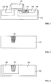
- Figures 2-7 illustrate cross-section structures of an exemplary LDMOS transistor corresponding to certain stages of the fabrication process consistent with the disclosed embodiments.
- Figure 8 illustrates an exemplary method for forming an LDMOS transistor consistent with the disclosed embodiments.
- a semiconductor substrate 200 is provided as a platform for forming an LDMOS transistor (e.g., Step 802 in Figure 8 ).
- the semiconductor substrate 200 may be made of any appropriate type of semiconductor materials, such as silicon (Si), germanium (Ge), silicon germanium (SiGe), carborundum (SiC), silicon on insulator (SOI), germanium on insulator (GOI), or gallium arsenide and other Group III-V compounds, or a combination thereof.
- the semiconductor substrate 200 is a silicon substrate.
- a shallow trench isolation structure 201 may be formed in the semiconductor substrate 200 (e.g., Step 804 in Figure 8 ) for increasing the channel length of the LDMOS transistor, which may in turn increase the breakdown voltage of the LDMOS transistor.
- the shallow trench isolation structure 201 may be formed by forming a mask layer (not shown) on the semiconductor substrate 200.
- the mask layer may have an opening to expose a surface of the semiconductor substrate 200.
- a groove may be formed in the semiconductor substrate 200 by etching along the opening in the mask layer.
- an insulation material layer may be formed that covers the mask layer and fills the groove. The insulation material layer may be planarized until the surface of the semiconductor substrate 200 is exposed and the shallow trench isolation structure 201 is formed in the groove.
- the shallow trench isolation structure 201 may have a single-layer structure or a multi-layer (e.g., having two or more layers) stack structure.
- the multi-layer stack structure may be a two-layer stack structure, for example, including a pad layer formed on the side and bottom surfaces of the groove and a filling layer formed on the pad layer to fill up the groove.
- the pad layer may be a silicon oxide layer and the filling layer may be a silicon nitride layer.
- a drift region 203 may be formed in the semiconductor substrate 200, and the drift region 203 may surround the shallow trench isolation structure 201 (e.g., Step 806 in Figure 8 ).
- a well region 202 may also be formed in the semiconductor substrate 200.
- the drift region 203 is then formed in the well region 202.
- the depth of the drift region 203 may be less than the depth of the well region 202.
- the well region 202 may be formed prior to forming the shallow trench isolation structure 201. Alternatively, the well region 202 may be formed after the shallow trench isolation structure 201 is formed.
- the well region 202 and the drift region 203 may be formed by an ion implantation process, and a mask layer may be formed on the semiconductor substrate 200 prior to forming the drift region 203.
- the mask layer may have an opening to expose a region of the semiconductor substrate 200 for the ion implantation.
- the well region 202 may be doped with N-type ions and the drift region 203 may be doped with P-type ions in forming a P-type LDMOS transistor.
- the well region 202 may be doped with P-type ions and the drift region 203 may be doped with N-type ions in forming an N-type LDMOS transistor.
- the N-type ions may include one or more of phosphorus ions, arsenic ions and antimony ions; and the P-type ions may include one or more of boron ions, indium ions and gallium ions.
- a body region 208 may be formed in the semiconductor substrate 200 on a side of the drift region 203 (e.g., Step 808 in Figure 8 ).
- the body region 208 may be formed by an ion implantation process.
- the body region 208 may be doped with N-type ions in forming a P-type LDMOS transistor.
- the body region 208 may be doped with P-type ions in forming an N-type LDMOS transistor.
- the N-type ions may include one or more of phosphorus ions, arsenic ions and antimony ions; and the P-type ions may include one or more of boron ions, indium ions and gallium ions.
- the body region 208 may be formed after the drift region 203 is formed. In other embodiments, the body region 208 may be formed prior to forming the drift region 203.
- a gate structure 207 may be formed on the semiconductor substrate 200.
- the gate structure 207 may cover a portion of the body region 208, a portion of the well region 202, a portion of the drift region 203, and a portion of the shallow trench isolation structure 201 (e.g., Step 810 in Figure 8 ).
- the gate structure 207 may include a gate dielectric layer 204 formed on the semiconductor substrate 200 and a gate electrode 206 formed on the gate dielectric layer 204.
- the gate dielectric layer 204 may be made of silicon oxide and the gate electrode 206 may be made of poly silicon.
- the gate structure 207 may be formed by: forming a gate dielectric material layer overlying the surface of the semiconductor substrate 200; forming a gate electrode material layer on the gate dielectric material layer; and etching the gate electrode material layer and the gate dielectric material layer to form the gate dielectric layer 204 on a portion of the body region 208, a portion of the drift region 203, a portion of the shallow trench isolation structure 201, and a surface portion of the semiconductor substrate 200 between the drift region 203 and the body region 208. After etching, the gate electrode 206 is formed on the gate dielectric layer 204.
- the gate dielectric layer 204 may be made of any appropriate material with high K value, such as HfO 2 , TiO 2 , HfZrO, HfSiNO or any combination thereof. Other materials may also be used according to various embodiments.
- the gate electrode 206 may be made of any appropriate metal, such as W, Cu, Al or any combination thereof. Other materials may also be used according to various embodiments.
- the gate structure 207 may be formed by a gate-last process.
- sidewall spacers 205 may be formed on both sides of the gate dielectric layer 204 and the gate electrode 206.
- the sidewall spacers 205 may protect both sides of the gate electrode 206 from being damaged when forming a first shallow doped region using an implantation process during the subsequent fabrication steps.
- the sidewall spacers 205 may control a location of a source region that may be subsequently formed in the body region 208.
- the sidewall spacers 205 may include a single-layer structure or a multi-layer (e.g., having two or more layers) structure.
- the sidewall spacers 205 may be made of silicon oxide, silicon nitride or other suitable materials.
- a drain region 209 may be formed in the drift region 203 adjacent to one side of the gate structure 207 (e.g., Step 812 in Figure 8 ); and a source region 210 may be formed in the body region 208 adjacent to the other side of the gate structure 207 (e.g., Step 814 in Figure 8 ).
- the drain region 209 and the source region 210 may be formed by a source-drain ion implantation process.
- the drain region 209 and the source region 210 may be doped with P-type ions in forming a P-type LDMOS transistor.
- the drain region 209 and the source region 210 may be doped with N-type ions in forming an N-type LDMOS transistor.
- the N-type ions may include one or more of phosphorus (P) ions, arsenic (As) ions and antimony (Sb) ions; and the P-type ions may include one or more of boron (B) ions, boron fluoride (BF 2 ) ions, indium (In) ions and gallium (Ga) ions.
- the implanted ions during the source-drain ion implantation process include one or more of B ions, BF 2 ions, Ga ions or In ions
- an implantation angle of approximately 0° ⁇ 5°, an implantation dose of approximately 5E13 atoms/cm 2 to 5E15 atoms/cm 2 , and an implantation energy of approximately 6Kev to 50Kev may be applied.
- the implanted ions during the source-drain ion implantation process include one or more of P ions, As ions, or Sb ions
- an implantation angle of approximately 0° ⁇ 5°, an implantation dose of approximately 5E13 atoms/cm 2 to 5E15 atoms/cm 2 , and an implantation energy of approximately 12Kev to 50Kev may be applied.
- a first shallow doped region 211 may be formed in the drain region 209 adjacent to one side of the gate structure 207 and in the drift region 203 adjacent to the bottom of the gate structure 207 (e.g., Step 816 in Figure 8 ).
- the first shallow doped region 211 and the drain region 209 may have a same doping type.
- the depth of the first shallow doped region 211 may be less than the depth of the drain region 209 and the depth of the drift region 203.
- the first shallow doped region 211 may include two portions, one portion located in the drain region 209 on one side of the gate structure 207 and the other portion located in the drift region 203 under the bottom of the gate structure 207.
- the first shallow doped region 211 may surround the shallow trench isolation structure 201.
- the formed first shallow doped region 211 may be used to improve the accumulation distribution of impurity ions, increase the uniformity of the impurity ion distribution in the drain region 209 and the drift region 203 surrounding the shallow trench isolation structure 201, and reduce the resistance in the vicinity of the surface of both the drain region 209 and the drift region 203 while preventing the impact of the local high resistance regions on the threshold voltage.
- the LDMOS transistor when the LDMOS transistor is in operating mode, the on-resistance of the channel between the drain region 209 and the source region 210 may be reduced. Therefore, when applying a same supply voltage to the drain region 209, the operating current of the disclosed LDMOS transistor may be increased compared to existing LDMOS transistors.
- the first shallow doped region 211 may have a depth of approximately 10 nm ⁇ 50 nm from a surface of the semiconductor substrate 200 and an ion doping concentration of approximately 1E18 atom/cm 3 to 1E19 atom/cm 3 .
- the first shallow doped region 211 may better improve the accumulation distribution of impurity ions due to the existence of the shallow trench isolation structure (STI) 201 in the drift region 203 and the drain region 209, increase the uniformity of the impurity ion distribution in the drain region 209 and the drift region 203 surrounding the shallow trench isolation structure 201, and reduce the resistance in the vicinity of the surface of both the drain region 209 and the drift region 203 while preventing the impact of the local high resistance regions on the threshold voltage.
- the depth of the first shallow doped region 211 refers to the vertical distance between the surface of the semiconductor substrate 200 and the bottom boundary of the first shallow doped region 211.
- the first shallow doped region 211 may be formed using a single-angle ion implantation process 21.
- implanted ions may be injected in a direction from the drain region 209 toward the source region 210.
- the implanted ion incident direction may have a first angle 31 made with the normal to the surface of the semiconductor substrate 200 as shown in Figure 7 , where the semiconductor substrate 200 is not rotated during the single-angle ion implantation process.
- Portions of the first shallow doped region 211 may be formed simultaneously in the vicinity of the surface of the drain region 209 on one side of the gate structure 207 and in the vicinity of the surface of the drift region 203 under the bottom of the gate structure 207 using the single-angle ion implantation.
- the process in forming the first shallow doped region 211 may be simplified.
- a mask layer may be formed on the semiconductor substrate 200 and the gate structure 207 prior to performing the single-angle ion implantation process.
- the mask layer may have an opening to expose the surface of the drain region 209 and the sidewall spacer 205 on the shallow trench isolation structure 201.
- the mask layer may be used as a mask for the single-angle ion implantation process.
- the first shallow doped region 211 may be doped with P-type ions in forming a P-type LDMOS transistor.
- BF 2 ions or B ions may be implanted using the single-angle ion implantation process.
- an implantation angle of approximately 15° ⁇ 40°, an implantation dose of approximately 1E13 atoms/cm 2 to 1E14 atoms/cm 2 , and implantation energy of approximately 5Kev to 40Kev may be applied.
- the implantation angle may be set to be 15°, 20°, 30°, or 35°; the implantation dose may be set to be 2E13 atoms/cm 2 , 3E13 atoms/cm 2 , 4E13 atoms/cm 2 , 5E13 atom /cm 2 , 6E13 atoms/cm 2 , 7E13 atoms/cm 2 , 8E13 atoms/cm 2 , or 9E13 atoms/cm 2 ; and the implantation energy may be set to be 10Kev, 15Kev, 20Kev, 25Kev, 30Kev, or 35Kev.
- the formed first shallow doped region 211 may have high space accuracy.
- the first shallow doped region 211 may effectively increase the uniformity of the impurity ion distribution in the drain region 209 and the drift region 203 surrounding the shallow trench isolation structure 201, and reduce the resistance in the vicinity of the surface of both the drain region 209 and the drift region 203.
- F ions therein may prevent the diffusion of B ions into the semiconductor substrate 200 between the drift region 203 and the body region 208 and, thus, may prevent short channel effects.
- diffusion-preventing ions such as C ions or N ions may also be implanted in the single-angle ion implantation process.
- the implanted C ions or N ions may prevent the diffusion of the implanted B ions into the semiconductor substrate 200 between the drift region 203 and the body region 208 and, thus, may prevent short channel effects.
- an implantation angle of approximately 15° ⁇ 40°, an implantation dose of approximately 5E12 atoms/cm 2 to 5E 15 atoms/cm 2 , and an implantation energy of approximately 0.5Kev to 20Kev may be applied.
- the implantation angle may be set to 10°, 20°, 30°, or 35°; the implantation dose may be set to 6E12 atoms/cm 2 , 9E12 atoms/cm 2 , 2E13 atoms/cm 2 , 5E13 atoms/cm 2 , 8E13 atoms/cm 2 , 9E13 atoms/cm 2 , 2E15 atoms/cm 2 , or 4E15 atoms/cm 2 ; and the implantation energy may be set to 1Kev, 2Kev, 5Kev, 10Kev, 12Kev, 14Kev, 15Kev, 17Kev, 18Kev, or 19Kev.
- the position of the implanted C ions or N ions may correspond to the location of the first shallow doped region 211 and the electrical properties of the first shallow doped region 211 is not affected.
- the implanted C ions or N ions may effectively prevent the diffusion of B ions in the first shallow doped region 211.
- the first shallow doped region 211 may be doped with N-type ions in forming an N-type LDMOS transistor.
- P ions or As ions may be implanted using the single-angle ion implantation process.
- an implantation angle of approximately 15° ⁇ 40°, an implantation dose of approximately 1E13 atoms/cm 2 to 1E14 atoms/cm 2 , and an implantation energy of approximately 8Kev to 45Kev may be applied.
- the formed first shallow doped region 211 may have high space accuracy.
- the first shallow doped region 211 may effectively increase the uniformity of the impurity ion distribution in the drain region 209 and the drift region 203 surrounding the shallow trench isolation structure 201, and reduce the resistance in the vicinity of the surface of both the drain region 209 and the drift region 203.
- diffusion-preventing ions such as C ions or N ions may also be implanted using the single-angle ion implantation process.
- the implanted C ions or N ions may prevent the diffusion of the implanted P ions or As ions from the first shallow doped region 211 into the semiconductor substrate 200 between the drift region 203 and the body region 208 and, thus, may prevent short channel effects.
- an implantation angle of approximately 15° ⁇ 40°, an implantation dose of approximately 5E12 atoms/cm 2 to 5E15 atoms/cm 2 , and implantation energy of approximately 0.5Kev to 20Kev may be applied.
- the position of the implanted C ions or N ions may correspond to the location of the first shallow doped region 211 and the electrical properties of the first shallow doped region 211 is not affected.
- the implanted C ions or N ions may effectively prevent the diffusion of P ions or As ions in the first shallow doped region 211.
- a second doped region 212 may be formed simultaneously in the source region 210.
- the doping type of the second doped region 212 may be the same as the doping type of the source region 210.
- the depth of the second doped region 212 may be less than the depth of the source region 210, and the second doped region 212 may have a first distance away from the adjacent sidewall spacer of the gate structure 207.
- the gate structure 207 may block a portion of the impurity ions to be injected toward the source region during the single-angle ion implantation process.
- the second doped region 212 may be formed away from the sidewall spacer 205 of the gate structure 207. That is, the body region 208 under the bottom of the gate structure 207 and the source region 210 will not be implanted with an inverted type of impurity ions, so as to reduce the resistance in the vicinity of the surface of the source region 210 while preventing short channel effects.
- the second doped region 212 may be implanted with ions same as for the first shallow doped region 211, e.g., by the single-angle ion implantation process.
- the second doped region 212 may also include diffusion-preventing ions, such as C ions or N ions.
- an annealing process may be performed to activate the doping ions.
- the annealing temperature may be in a range of approximately 900 °C ⁇ 1100 °C, and the annealing time may be in a range of approximately 10 seconds to 30 seconds.
- the first shallow doped region 211 may be formed in the drain region 209 on one side of the gate structure 207 and in the drift region 203 under the bottom of the gate structure 207.
- the first shallow doped region 211 may be formed prior to forming the gate structure 207.
- the first shallow doped region 211 may be formed by: forming a drift region 203 in the semiconductor substrate 200, the drift region 203 surrounding the shallow trench isolation structure 201; forming a first shallow doped region 211 in the drift region 203, the first shallow doped region 211 surrounding the shallow trench isolation structure 201, where the first shallow doped region 211 may have the same doping type as that of the drain region 209 and the depth of the first shallow doped region 211 may be less than the depth of the drift region 203; forming a body region 208 in the semiconductor substrate 200 on a side of the drift region 203; forming a gate structure 207 on a portion of the body region 208, a portion of the drift region 203, a portion of the well region 202 in the semiconductor substrate 200, and a portion of the shallow trench isolation structure 201; forming a drain region 209 in the drift region 203 adjacent to one side of the gate structure 207
- the first shallow doped region 211 is formed before the formation of the gate structure 207, the impact of the gate structure 207 on the position, the concentration of impurity ions and the uniformity of the distribution of impurity ions of the first shallow doped region 211 may be prevented. Thus, the position accuracy of the first shallow doped region 211 and the uniformity of the impurity ion distribution in the first shallow doped region 211 may be improved.
- the first shallow doped region 211 may be formed by an ion implantation process. A same mask may be used in forming the first shallow doped region 211 and the drift region 203. Although a non-zero implantation angle is used for forming the first shallow doped region 211 as described above, the first shallow doped region 211 may be formed by an ion implantation having a 0° incident angle (the implantation direction is perpendicular to the semiconductor substrate surface). Other process features are substantially the same as those described for forming the first shallow doped region 211 in the present invention. It is to be noted that, in this embodiment, the other features of the respective structures may also be referred to the features of the corresponding structures in the present invention, and the description thereof will not be repeated herein.
- the LDMOS transistor may include: a semiconductor substrate 200; a shallow trench isolation structure 201 located in the semiconductor substrate 200; a drift region 203 located in the semiconductor substrate 200, the drift region 203 surrounding the shallow trench isolation structure 201; a body region 208 located in the semiconductor substrate 200 on a side of the drift region 203; a gate structure 207 on a portion of the body region 208, a portion of the drift region 203, and a portion of the shallow trench isolation structure 201; a drain region 209 located in the drift region 203 on one side of the gate structure 207; a source region 210 located in the body region 208 on the other side of the gate structure 207; and a first shallow doped region 211 located in the drain region 209 on one side of the gate structure 207 and in the drift region 203 under the bottom of the gate structure 207.
- the doping type of the first shallow doped region 211 may be the same as that of the drain region 20
- the first shallow doped region 211 may have a depth of approximately 10nm ⁇ 50nm and an ion doping concentration of approximately 1E18 atom/cm 3 to 1E19atom/cm 3 .
- the doping type of the body region 208 is N-type
- the doping type of the drift region 203 is P-type
- the doping type of the drain region 209 is P-type
- the doping type of the shallow doped region 211 is P-type
- the doping type of the source region 210 is P-type.
- the doping type of the body region 208 is P-type
- the doping type of the drift region 203 is N-type
- the doping type of the drain region 209 is N-type
- the doping type of the shallow doped region 211 is N-type
- the doping type of the source region 210 is N-type.
Landscapes
- Insulated Gate Type Field-Effect Transistor (AREA)
- Chemical & Material Sciences (AREA)
- Crystallography & Structural Chemistry (AREA)
Abstract
Description
- This application claims the priority of Chinese patent application No.
CN201610504769.6, filed on June 30, 2016 - The present invention generally relates to the field of semiconductor manufacturing technology and, more particularly, relates to a Lateral Double-Diffused MOSFET (LDMOS) transistor and a method of forming the LDMOS transistor.
- In the semiconductor industry, there are mainly two types of power MOSFET, namely a Vertical Double-Diffused MOSFET (VDMOS) and a Lateral Double-Diffused MOSFET (LDMOS). Among them, LDMOS transistors may have many advantages over VDMOS transistors. For example, LDMOS transistors may have better thermal and frequency stability, higher gain and ruggedness, lower feedback capacitance and thermal resistance, as well as constant input impedance and a simpler bias current circuitry.
- A typical N-type LDMOS structure is shown in
Figure 1 . It includes a semiconductor substrate (not shown) and a P-well 100 created in the semiconductor substrate; an N-type drift region 101 formed within the P-well 100; a shallowtrench isolation structure 104 formed within the N-type drift region 101 for increasing the channel length of the LDMOS transistor, which may in turn increase the breakdown voltage of the LDMOS transistor; a P-type body region 106 formed within the P-well 100 on side of the N-type drift region 101; agate structure 105 formed on the semiconductor substrate where thegate structure 105 laterally on the P-type body region 106 and the N-type Driftregion 101 and covers a portion of the shallowtrench isolation structure 104. Thegate structure 105 may include a gate dielectric layer formed on the semiconductor substrate, a gate electrode formed on the gate dielectric layer, and sidewall spacers formed on both sides of the gate dielectric layer and the gate electrode. Adrain region 103 is formed in the N-type drift region 101 along with asource region 102 formed in the p-type body region 106, where thesource region 102 and thedrain region 103 are located on two sides of the gate structure, respectively, and adjacent to thegate structure 105. Both thesource region 102 and thedrain region 103 are formed with N-type doping. - It is an object of the present invention to provide a transistor and a corresponding fabrication method which may solve one or more problems of the current LDMOS transistors, in particular can improve the performance of the existing LDMOS transistors , for example, in which the operating current of the existing LDMOS transistors can be increased.
- The object is achieved by the features of the respective independent claims. Further embodiments are defined in the respective dependent claims.
- A first aspect of the present invention provides a method of forming a lateral double-diffused MOSFET transistor. In the method, a shallow trench isolation structure is formed in a semiconductor substrate. A drift region is formed in the semiconductor substrate, the drift region surrounding the shallow trench isolation structure. A body region is formed in the semiconductor substrate and distanced from the drift region. A gate structure is formed on a portion of each of the body region, the drift region, and the shallow trench isolation structure. A drain region is formed in the drift region on one side of the gate structure. A source region is formed in the body region on another side of the gate structure. A first shallow doped region is formed in the drain region and the drift region to surround the shallow trench isolation structure, the first shallow doped region having a same doping type as for the drain region and a depth less than the drain region and the drift region.
- Preferably, the method further includes: performing a single-angle ion implantation process for forming the first shallow doped region without rotating the semiconductor substrate, the single-angle ion implantation process injecting ions in a direction from the drain region toward the source region with a first angle between an implanted ion incident direction and a normal to a surface of the semiconductor substrate.
- Preferably, the first shallow doped region has a depth of approximately 10nm∼50nm and an ion doping concentration of approximately 1E18 atom/cm3 to 1E19 atom/cm3.
- Preferably, the method further includes: forming a second doped region in the source region simultaneously when forming the first shallow doped region, wherein the second doped region has a first distance away from an adjacent side of the gate structure; and the second doped region has a same doping type as that of the source region and a depth less than the source region.
- According to a first particular embodiment, the LDMOS transistor is a P-type LDMOS transistor.
- Preferably, the doping type of the body region is N-type.
- Preferably, the doping type of the drift region is P-type.
- Preferably, the doping type of the drain region is P-type.
- Preferably, the doping type of the first shallow doped region is P-type.
- Preferably, the doping type of the source region is P-type.
- Preferably, BF2 ions or B ions are implanted to form the first shallow doped region using a single-angle ion implantation process.
- Preferably, the method further includes: employing an implantation angle of approximately 15° to 40°, an implantation dose of approximately 1E13 atoms/cm2 to 1E14 atoms/cm2, and an implantation energy of approximately 5Kev to 40Kev for implanting BF2 ions or B ions.
- Preferably, the method further includes: implanting diffusion-preventing ions during the single-angle ion implantation process, wherein the diffusion-preventing ions include C ions or N ions.
- Preferably, the method further includes: employing an implantation angle of approximately 15° to 40°, an implantation dose of approximately 5E12 atoms/cm2 to 5E15 atoms/cm2, and an implantation energy of approximately 0.5Kev to 20Kev for implanting C ions or N ions.
- Preferably, a source-drain ion implantation process is performed for forming the source region and the drain region, the source-drain ion implantation process implanting one or more of B ions, BF2 ions, Ga ions and In ions with an implantation angle of approximately 0°∼5°, an implantation dose of approximately 5E13 atoms/cm2 to 5E15 atoms/cm2, and an implantation energy of approximately 6Kev to 50Kev.
- According to second particular embodiment, the LDMOS transistor is an N-type LDMOS transistor.
- Preferably, the doping type of the body region is P-type.
- Preferably, the doping type of the drift region is N-type.
- Preferably, the doping type of the drain region is N-type.
- Preferably, the doping type of the first shallow doped region is N-type.
- Preferably, the doping type of the source region is N-type.
- Preferably, P ions or As ions are implanted to form the first shallow doped region using a single-angle ion implantation process.
- Preferably, the method further includes: employing an implantation angle of approximately 15° to 40°, an implantation dose of approximately 1E13 atoms/cm2 to 1E14 atoms/cm2, and an implantation energy of approximately 8Kev to 45Kev for implanting P ions or As ions.
- Preferably, the method further includes: implanting diffusion-preventing ions during the single-angle ion implantation process, wherein the diffusion-preventing ions include C ions or N ions.
- Preferably, the method further includes: employing an implantation angle of approximately 15° to 40°, an implantation dose of approximately 5E12 atoms/cm2 to 5E15 atoms/cm2, and an implantation energy of approximately 0.5Kev to 20Kev for implanting C ions or N ions.
- Preferably, a source-drain ion implantation process is performed in forming the source region and the drain region, the source-drain ion implantation process implanting one or more of P ions, As ions, and Sb ions with an implantation angle of approximately 0°∼5°, an implantation dose of approximately 5E13 atoms/cm2 to 5E15 atoms/cm2, and an implantation energy of approximately 12Kev to 50Kev.
- A second aspect of the present invention provides an LDMOS transistor. The LDMOS transistor includes a semiconductor substrate; a shallow trench isolation structure in the semiconductor substrate; a drift region located in the semiconductor substrate and surrounding the shallow trench isolation structure; a body region located in the semiconductor substrate and distanced from the drift region; a gate structure on a portion of each of the body region, the drift region, and the shallow trench isolation structure; a drain region located in the drift region on one side of the gate structure; a source region located in the body region on an other side of the gate structure; and a first shallow doped region located in the drain region and in the drift region to surround the shallow trench isolation structure, the first shallow doped region having a same doping type as that of the drain region and a depth less than the drain region and the drift region.
- Preferably, the first shallow doped region has a depth of approximately 10nm∼50nm and an ion doping concentration of approximately 1E18 atom/cm3 to 1E19 atom/cm3.
- Preferably, LDMOS transistor further includes: a second doped region in the source region, wherein: the second doped region has a first distance away from an adjacent side of the gate structure and has a depth less than the source region.
- Preferably, the first shallow doped region further includes diffusion-preventing ions.
- Preferably, the diffusion-preventing ions include C ions or N ions.
- A transistor according to the second aspect of the present invention may be obtained by a method according to the first aspect of the present invention.
- Other aspects of the present invention can be understood by those skilled in the art in light of the description, the claims, and the drawings of the present invention.
- The following drawings are merely examples for illustrative purposes according to various disclosed embodiments and are not intended to limit the present invention.
-
Figure 1 illustrates an existing LDMOS transistor; -
Figures 2-7 illustrate cross-section structures of an exemplary LDMOS transistor corresponding to certain stages of the fabrication process consistent with the disclosed embodiments; and -
Figure 8 illustrates an exemplary method for forming an LDMOS transistor consistent with the disclosed embodiments. - As stated in the background section, the performance of existing LDMOS transistors still needs to be improved. For example, the operating current of the existing LDMOS transistors still needs to be increased.
- In current technologies, the operating current of an LDMOS transistor may be limited by an on-resistance between the source region and the drain region of the LDMOS transistor and may be difficult to be increased further. Although it may be possible to increase the operating current by decreasing the size (e.g., length) of the channel between the source and drain regions or by increasing the doping dose in the source and drain regions, the corresponding breakdown voltage of the LDMOS transistor may be reduced and may cause short channel effects or other effects on electrical properties.
- Furthermore, it is found that when a current process is used to form the source and drain regions by an ion implantation, the channel threshold voltage is usually adjusted by a uniform channel surface ion implantation process. This ion implantation process may result in a large channel resistance that may suppress the operating current of the LDMOS transistor. In the meantime, due to the existence of the shallow trench isolation structure (STI) in the drift region and the drain region using the current process, the accumulation distribution of the impurity ions (uneven distribution of impurity ions) may lead to local high resistance in the drift region and the drain region, and may affect the channel threshold voltage and operating current. While adjusting channel ion implantation may reduce the threshold voltage to improve the operating current, it would be difficult to make the operating voltage and operating current meet the requirements at the same time and to improve the uniformity of the impurity ion distribution.
- The present invention provides an LDMOS transistor and a method of forming the same. The method of forming the LDMOS transistor may include forming a first shallow doped region in the drain region adjacent to one side of the gate structure and in the drift region adjacent to the bottom of the gate structure. The first shallow doped region and the drain region may have a same doping type. The depth of the first shallow doped region may be less than the depth of the drain region and the depth of the drift region.
- The presence of the first shallow doped region as disclosed herein may improve the accumulation distribution of impurity ions in the drift region and the drain region caused by the existence of the shallow trench isolation structure (STI), and may increase the uniformity of the impurity ion distribution in the drain region surrounding the shallow trench isolation structure and the drift region, and reduce the resistance in the vicinity of the surface of both the drain region and the drift region while preventing the impact of the local high resistance regions on the threshold voltage. Thus, when the LDMOS transistor is in operating mode, the on-resistance of the channel between the drain region and the source region may be reduced. Therefore, when applying a same supply voltage to the drain region, the operating current of the LDMOS transistor may be increased compared to using existing technologies. Further, by forming a first shallow doped region, the disclosed transistor and method may effectively prevent the impact of the local high resistance regions on the effective channel and reduce short channel effects while improving the channel doing uniformity through the impurity supplement principle.
- The foregoing and other objects, features and advantages of the present invention will become more apparent from the following detailed description when taken in conjunction with the accompanying drawings. While the embodiments of the present invention are described in detail, the illustrations are not exaggerated in a generalized scale for convenience of explanation, and the illustrations are merely exemplary and should not limit the present invention. In addition, the actual fabrication should include the length, width and depth of the three-dimensional parameters.
-
Figures 2-7 illustrate cross-section structures of an exemplary LDMOS transistor corresponding to certain stages of the fabrication process consistent with the disclosed embodiments.Figure 8 illustrates an exemplary method for forming an LDMOS transistor consistent with the disclosed embodiments. - As shown in
Figure 2 , asemiconductor substrate 200 is provided as a platform for forming an LDMOS transistor (e.g., Step 802 inFigure 8 ). Thesemiconductor substrate 200 may be made of any appropriate type of semiconductor materials, such as silicon (Si), germanium (Ge), silicon germanium (SiGe), carborundum (SiC), silicon on insulator (SOI), germanium on insulator (GOI), or gallium arsenide and other Group III-V compounds, or a combination thereof. In one embodiment, thesemiconductor substrate 200 is a silicon substrate. - A shallow
trench isolation structure 201 may be formed in the semiconductor substrate 200 (e.g., Step 804 inFigure 8 ) for increasing the channel length of the LDMOS transistor, which may in turn increase the breakdown voltage of the LDMOS transistor. - In one embodiment, the shallow
trench isolation structure 201 may be formed by forming a mask layer (not shown) on thesemiconductor substrate 200. The mask layer may have an opening to expose a surface of thesemiconductor substrate 200. Then, a groove may be formed in thesemiconductor substrate 200 by etching along the opening in the mask layer. Further, an insulation material layer may be formed that covers the mask layer and fills the groove. The insulation material layer may be planarized until the surface of thesemiconductor substrate 200 is exposed and the shallowtrench isolation structure 201 is formed in the groove. - The shallow
trench isolation structure 201 may have a single-layer structure or a multi-layer (e.g., having two or more layers) stack structure. In one embodiment, the multi-layer stack structure may be a two-layer stack structure, for example, including a pad layer formed on the side and bottom surfaces of the groove and a filling layer formed on the pad layer to fill up the groove. In one embodiment, the pad layer may be a silicon oxide layer and the filling layer may be a silicon nitride layer. - As shown in
Figure 3 , adrift region 203 may be formed in thesemiconductor substrate 200, and thedrift region 203 may surround the shallow trench isolation structure 201 (e.g.,Step 806 inFigure 8 ). - Before forming the
drift region 203, awell region 202 may also be formed in thesemiconductor substrate 200. Thedrift region 203 is then formed in thewell region 202. The depth of thedrift region 203 may be less than the depth of thewell region 202. Thewell region 202 may be formed prior to forming the shallowtrench isolation structure 201. Alternatively, thewell region 202 may be formed after the shallowtrench isolation structure 201 is formed. - In one embodiment, the
well region 202 and thedrift region 203 may be formed by an ion implantation process, and a mask layer may be formed on thesemiconductor substrate 200 prior to forming thedrift region 203. The mask layer may have an opening to expose a region of thesemiconductor substrate 200 for the ion implantation. In one embodiment, thewell region 202 may be doped with N-type ions and thedrift region 203 may be doped with P-type ions in forming a P-type LDMOS transistor. In another embodiment, thewell region 202 may be doped with P-type ions and thedrift region 203 may be doped with N-type ions in forming an N-type LDMOS transistor. The N-type ions may include one or more of phosphorus ions, arsenic ions and antimony ions; and the P-type ions may include one or more of boron ions, indium ions and gallium ions. - As shown in
Figure 4 , abody region 208 may be formed in thesemiconductor substrate 200 on a side of the drift region 203 (e.g., Step 808 inFigure 8 ). Thebody region 208 may be formed by an ion implantation process. In one embodiment, thebody region 208 may be doped with N-type ions in forming a P-type LDMOS transistor. In another embodiment, thebody region 208 may be doped with P-type ions in forming an N-type LDMOS transistor. The N-type ions may include one or more of phosphorus ions, arsenic ions and antimony ions; and the P-type ions may include one or more of boron ions, indium ions and gallium ions. - In some embodiments, the
body region 208 may be formed after thedrift region 203 is formed. In other embodiments, thebody region 208 may be formed prior to forming thedrift region 203. - As shown in
Figure 5 , agate structure 207 may be formed on thesemiconductor substrate 200. Thegate structure 207 may cover a portion of thebody region 208, a portion of thewell region 202, a portion of thedrift region 203, and a portion of the shallow trench isolation structure 201 (e.g., Step 810 inFigure 8 ). - In one embodiment, the
gate structure 207 may include agate dielectric layer 204 formed on thesemiconductor substrate 200 and agate electrode 206 formed on thegate dielectric layer 204. - In one embodiment, the
gate dielectric layer 204 may be made of silicon oxide and thegate electrode 206 may be made of poly silicon. Thegate structure 207 may be formed by: forming a gate dielectric material layer overlying the surface of thesemiconductor substrate 200; forming a gate electrode material layer on the gate dielectric material layer; and etching the gate electrode material layer and the gate dielectric material layer to form thegate dielectric layer 204 on a portion of thebody region 208, a portion of thedrift region 203, a portion of the shallowtrench isolation structure 201, and a surface portion of thesemiconductor substrate 200 between thedrift region 203 and thebody region 208. After etching, thegate electrode 206 is formed on thegate dielectric layer 204. - In other embodiments, the
gate dielectric layer 204 may be made of any appropriate material with high K value, such as HfO2, TiO2, HfZrO, HfSiNO or any combination thereof. Other materials may also be used according to various embodiments. Additionally, thegate electrode 206 may be made of any appropriate metal, such as W, Cu, Al or any combination thereof. Other materials may also be used according to various embodiments. In one embodiment, thegate structure 207 may be formed by a gate-last process. - Further, in one embodiment,
sidewall spacers 205 may be formed on both sides of thegate dielectric layer 204 and thegate electrode 206. The sidewall spacers 205 may protect both sides of thegate electrode 206 from being damaged when forming a first shallow doped region using an implantation process during the subsequent fabrication steps. Moreover, thesidewall spacers 205 may control a location of a source region that may be subsequently formed in thebody region 208. The sidewall spacers 205 may include a single-layer structure or a multi-layer (e.g., having two or more layers) structure. The sidewall spacers 205 may be made of silicon oxide, silicon nitride or other suitable materials. - As shown in
Figure 6 , adrain region 209 may be formed in thedrift region 203 adjacent to one side of the gate structure 207 (e.g., Step 812 inFigure 8 ); and asource region 210 may be formed in thebody region 208 adjacent to the other side of the gate structure 207 (e.g., Step 814 inFigure 8 ). - The
drain region 209 and thesource region 210 may be formed by a source-drain ion implantation process. In one embodiment, thedrain region 209 and thesource region 210 may be doped with P-type ions in forming a P-type LDMOS transistor. In another embodiment, thedrain region 209 and thesource region 210 may be doped with N-type ions in forming an N-type LDMOS transistor. The N-type ions may include one or more of phosphorus (P) ions, arsenic (As) ions and antimony (Sb) ions; and the P-type ions may include one or more of boron (B) ions, boron fluoride (BF2) ions, indium (In) ions and gallium (Ga) ions. - In one embodiment, when the implanted ions during the source-drain ion implantation process include one or more of B ions, BF2 ions, Ga ions or In ions, an implantation angle of approximately 0°∼5°, an implantation dose of approximately 5E13 atoms/cm2 to 5E15 atoms/cm2, and an implantation energy of approximately 6Kev to 50Kev may be applied.
- In another embodiment, when the implanted ions during the source-drain ion implantation process include one or more of P ions, As ions, or Sb ions, an implantation angle of approximately 0°∼5°, an implantation dose of approximately 5E13 atoms/cm2 to 5E15 atoms/cm2, and an implantation energy of approximately 12Kev to 50Kev may be applied.
- As shown in
Figure 7 , a first shallow dopedregion 211 may be formed in thedrain region 209 adjacent to one side of thegate structure 207 and in thedrift region 203 adjacent to the bottom of the gate structure 207 (e.g., Step 816 inFigure 8 ). The first shallow dopedregion 211 and thedrain region 209 may have a same doping type. The depth of the first shallow dopedregion 211 may be less than the depth of thedrain region 209 and the depth of thedrift region 203. - The first shallow doped
region 211 may include two portions, one portion located in thedrain region 209 on one side of thegate structure 207 and the other portion located in thedrift region 203 under the bottom of thegate structure 207. The first shallow dopedregion 211 may surround the shallowtrench isolation structure 201. While the existence of the shallow trench isolation (STI)structure 201 may often lead to an accumulation distribution of impurity ions in thedrift region 203 and thedrain region 209, the formed first shallow dopedregion 211 may be used to improve the accumulation distribution of impurity ions, increase the uniformity of the impurity ion distribution in thedrain region 209 and thedrift region 203 surrounding the shallowtrench isolation structure 201, and reduce the resistance in the vicinity of the surface of both thedrain region 209 and thedrift region 203 while preventing the impact of the local high resistance regions on the threshold voltage. Thus, when the LDMOS transistor is in operating mode, the on-resistance of the channel between thedrain region 209 and thesource region 210 may be reduced. Therefore, when applying a same supply voltage to thedrain region 209, the operating current of the disclosed LDMOS transistor may be increased compared to existing LDMOS transistors. - In one embodiment, the first shallow doped
region 211 may have a depth of approximately 10 nm ∼ 50 nm from a surface of thesemiconductor substrate 200 and an ion doping concentration of approximately 1E18 atom/cm3 to 1E19 atom/cm3. Thus, the first shallow dopedregion 211 may better improve the accumulation distribution of impurity ions due to the existence of the shallow trench isolation structure (STI) 201 in thedrift region 203 and thedrain region 209, increase the uniformity of the impurity ion distribution in thedrain region 209 and thedrift region 203 surrounding the shallowtrench isolation structure 201, and reduce the resistance in the vicinity of the surface of both thedrain region 209 and thedrift region 203 while preventing the impact of the local high resistance regions on the threshold voltage. It should be noted that the depth of the first shallow dopedregion 211 refers to the vertical distance between the surface of thesemiconductor substrate 200 and the bottom boundary of the first shallow dopedregion 211. - The first shallow doped
region 211 may be formed using a single-angleion implantation process 21. In the single-angle ion implantation process, implanted ions may be injected in a direction from thedrain region 209 toward thesource region 210. The implanted ion incident direction may have afirst angle 31 made with the normal to the surface of thesemiconductor substrate 200 as shown inFigure 7 , where thesemiconductor substrate 200 is not rotated during the single-angle ion implantation process. Portions of the first shallow dopedregion 211 may be formed simultaneously in the vicinity of the surface of thedrain region 209 on one side of thegate structure 207 and in the vicinity of the surface of thedrift region 203 under the bottom of thegate structure 207 using the single-angle ion implantation. Thus, the process in forming the first shallow dopedregion 211 may be simplified. - In one embodiment, a mask layer may be formed on the
semiconductor substrate 200 and thegate structure 207 prior to performing the single-angle ion implantation process. The mask layer may have an opening to expose the surface of thedrain region 209 and thesidewall spacer 205 on the shallowtrench isolation structure 201. The mask layer may be used as a mask for the single-angle ion implantation process. - The first shallow doped
region 211 may be doped with P-type ions in forming a P-type LDMOS transistor. In one embodiment, BF2 ions or B ions may be implanted using the single-angle ion implantation process. When BF2 ions are being implanted, an implantation angle of approximately 15°∼40°, an implantation dose of approximately 1E13 atoms/cm2 to 1E14 atoms/cm2, and implantation energy of approximately 5Kev to 40Kev may be applied. For example, the implantation angle may be set to be 15°, 20°, 30°, or 35°; the implantation dose may be set to be 2E13 atoms/cm2, 3E13 atoms/cm2, 4E13 atoms/cm2, 5E13 atom /cm2, 6E13 atoms/cm2, 7E13 atoms/cm2, 8E13 atoms/cm2, or 9E13 atoms/cm2; and the implantation energy may be set to be 10Kev, 15Kev, 20Kev, 25Kev, 30Kev, or 35Kev. Thus, the formed first shallow dopedregion 211 may have high space accuracy. The first shallow dopedregion 211 may effectively increase the uniformity of the impurity ion distribution in thedrain region 209 and thedrift region 203 surrounding the shallowtrench isolation structure 201, and reduce the resistance in the vicinity of the surface of both thedrain region 209 and thedrift region 203. In addition, when the implanted ions are BF2 ions, F ions therein may prevent the diffusion of B ions into thesemiconductor substrate 200 between thedrift region 203 and thebody region 208 and, thus, may prevent short channel effects. - In another embodiment, in addition to BF2 ions or B ions, diffusion-preventing ions such as C ions or N ions may also be implanted in the single-angle ion implantation process. The implanted C ions or N ions may prevent the diffusion of the implanted B ions into the
semiconductor substrate 200 between thedrift region 203 and thebody region 208 and, thus, may prevent short channel effects. When C ions or N ions are being implanted, an implantation angle of approximately 15°∼40°, an implantation dose of approximately 5E12 atoms/cm2 to 5E15 atoms/cm2, and an implantation energy of approximately 0.5Kev to 20Kev may be applied. For example, the implantation angle may be set to 10°, 20°, 30°, or 35°; the implantation dose may be set to 6E12 atoms/cm2, 9E12 atoms/cm2, 2E13 atoms/cm2, 5E13 atoms/cm2, 8E13 atoms/cm2, 9E13 atoms/cm2, 2E15 atoms/cm2, or 4E15 atoms/cm2; and the implantation energy may be set to 1Kev, 2Kev, 5Kev, 10Kev, 12Kev, 14Kev, 15Kev, 17Kev, 18Kev, or 19Kev. Thus, the position of the implanted C ions or N ions may correspond to the location of the first shallow dopedregion 211 and the electrical properties of the first shallow dopedregion 211 is not affected. In addition, the implanted C ions or N ions may effectively prevent the diffusion of B ions in the first shallow dopedregion 211. - In yet another embodiment, the first shallow doped
region 211 may be doped with N-type ions in forming an N-type LDMOS transistor. P ions or As ions may be implanted using the single-angle ion implantation process. When P ions or As ions are being implanted, an implantation angle of approximately 15°∼40°, an implantation dose of approximately 1E13 atoms/cm2 to 1E14 atoms/cm2, and an implantation energy of approximately 8Kev to 45Kev may be applied. Thus, the formed first shallow dopedregion 211 may have high space accuracy. The first shallow dopedregion 211 may effectively increase the uniformity of the impurity ion distribution in thedrain region 209 and thedrift region 203 surrounding the shallowtrench isolation structure 201, and reduce the resistance in the vicinity of the surface of both thedrain region 209 and thedrift region 203. - In one embodiment, in addition to P ions or As ions, diffusion-preventing ions such as C ions or N ions may also be implanted using the single-angle ion implantation process. The implanted C ions or N ions may prevent the diffusion of the implanted P ions or As ions from the first shallow doped
region 211 into thesemiconductor substrate 200 between thedrift region 203 and thebody region 208 and, thus, may prevent short channel effects. When C ions or N ions are being implanted, an implantation angle of approximately 15° ∼ 40°, an implantation dose of approximately 5E12 atoms/cm2 to 5E15 atoms/cm2, and implantation energy of approximately 0.5Kev to 20Kev may be applied. Thus, the position of the implanted C ions or N ions may correspond to the location of the first shallow dopedregion 211 and the electrical properties of the first shallow dopedregion 211 is not affected. In addition, the implanted C ions or N ions may effectively prevent the diffusion of P ions or As ions in the first shallow dopedregion 211. - In other embodiments, when the first shallow doped
region 211 is formed using the single-angle ion implantation process, a seconddoped region 212 may be formed simultaneously in thesource region 210. The doping type of the seconddoped region 212 may be the same as the doping type of thesource region 210. The depth of the seconddoped region 212 may be less than the depth of thesource region 210, and the seconddoped region 212 may have a first distance away from the adjacent sidewall spacer of thegate structure 207. Since the seconddoped region 212 may be formed simultaneously with the first shallow dopedregion 211 and thesemiconductor substrate 200 is not rotated, thegate structure 207 may block a portion of the impurity ions to be injected toward the source region during the single-angle ion implantation process. Thus, the seconddoped region 212 may be formed away from thesidewall spacer 205 of thegate structure 207. That is, thebody region 208 under the bottom of thegate structure 207 and thesource region 210 will not be implanted with an inverted type of impurity ions, so as to reduce the resistance in the vicinity of the surface of thesource region 210 while preventing short channel effects. - In various embodiments, the second
doped region 212 may be implanted with ions same as for the first shallow dopedregion 211, e.g., by the single-angle ion implantation process. For example, the seconddoped region 212 may also include diffusion-preventing ions, such as C ions or N ions. - After the single-angle ion implantation process, an annealing process may be performed to activate the doping ions. In one embodiment, the annealing temperature may be in a range of approximately 900 °C ∼ 1100 °C, and the annealing time may be in a range of approximately 10 seconds to 30 seconds.
- As such, after the
gate structure 207 is formed, the first shallow dopedregion 211 may be formed in thedrain region 209 on one side of thegate structure 207 and in thedrift region 203 under the bottom of thegate structure 207. - In one embodiment, the first shallow doped
region 211 may be formed prior to forming thegate structure 207. The first shallow dopedregion 211 may be formed by: forming adrift region 203 in thesemiconductor substrate 200, thedrift region 203 surrounding the shallowtrench isolation structure 201; forming a first shallow dopedregion 211 in thedrift region 203, the first shallow dopedregion 211 surrounding the shallowtrench isolation structure 201, where the first shallow dopedregion 211 may have the same doping type as that of thedrain region 209 and the depth of the first shallow dopedregion 211 may be less than the depth of thedrift region 203; forming abody region 208 in thesemiconductor substrate 200 on a side of thedrift region 203; forming agate structure 207 on a portion of thebody region 208, a portion of thedrift region 203, a portion of thewell region 202 in thesemiconductor substrate 200, and a portion of the shallowtrench isolation structure 201; forming adrain region 209 in thedrift region 203 adjacent to one side of thegate structure 207, the depth of thedrain region 209 being greater than the depth of the first shallow dopedregion 211 but less than the depth of thedrift region 203; and forming asource region 210 in thebody region 208 on the other side of thegate structure 207. In this embodiment, since the first shallow dopedregion 211 is formed before the formation of thegate structure 207, the impact of thegate structure 207 on the position, the concentration of impurity ions and the uniformity of the distribution of impurity ions of the first shallow dopedregion 211 may be prevented. Thus, the position accuracy of the first shallow dopedregion 211 and the uniformity of the impurity ion distribution in the first shallow dopedregion 211 may be improved. - The first shallow doped
region 211 may be formed by an ion implantation process. A same mask may be used in forming the first shallow dopedregion 211 and thedrift region 203. Although a non-zero implantation angle is used for forming the first shallow dopedregion 211 as described above, the first shallow dopedregion 211 may be formed by an ion implantation having a 0° incident angle (the implantation direction is perpendicular to the semiconductor substrate surface). Other process features are substantially the same as those described for forming the first shallow dopedregion 211 in the present invention. It is to be noted that, in this embodiment, the other features of the respective structures may also be referred to the features of the corresponding structures in the present invention, and the description thereof will not be repeated herein. - The present invention also provides an LDMOS transistor. As shown in
Figure 7 , in one embodiment, the LDMOS transistor may include: asemiconductor substrate 200; a shallowtrench isolation structure 201 located in thesemiconductor substrate 200; adrift region 203 located in thesemiconductor substrate 200, thedrift region 203 surrounding the shallowtrench isolation structure 201; abody region 208 located in thesemiconductor substrate 200 on a side of thedrift region 203; agate structure 207 on a portion of thebody region 208, a portion of thedrift region 203, and a portion of the shallowtrench isolation structure 201; adrain region 209 located in thedrift region 203 on one side of thegate structure 207; asource region 210 located in thebody region 208 on the other side of thegate structure 207; and a first shallow dopedregion 211 located in thedrain region 209 on one side of thegate structure 207 and in thedrift region 203 under the bottom of thegate structure 207. The doping type of the first shallow dopedregion 211 may be the same as that of thedrain region 209, and the depth of the first shallow dopedregion 211 is less than that of thedrain region 209 and thedrift region 203. - The first shallow doped
region 211 may have a depth of approximately 10nm∼50nm and an ion doping concentration of approximately 1E18 atom/cm3 to 1E19atom/cm3. - When the LDMOS transistor is a P-type LDMOS transistor, the doping type of the
body region 208 is N-type, the doping type of thedrift region 203 is P-type, the doping type of thedrain region 209 is P-type, the doping type of the shallowdoped region 211 is P-type, and the doping type of thesource region 210 is P-type. - When the LDMOS transistor is an N-type LDMOS transistor, the doping type of the
body region 208 is P-type, the doping type of thedrift region 203 is N-type, the doping type of thedrain region 209 is N-type, the doping type of the shallowdoped region 211 is N-type, and the doping type of thesource region 210 is N-type. - It should be noted that, other features and descriptions regarding the LDMOS transistor are referred to the corresponding features and descriptions for forming the LDMOS transistor in the present invention.
Claims (15)
- A method of forming a lateral double-diffused MOSFET, LDMOS, transistor, comprising:forming a shallow trench isolation structure in a semiconductor substrate;forming a drift region in the semiconductor substrate, the drift region surrounding the shallow trench isolation structure;forming a body region in the semiconductor substrate and distanced from the drift region;forming a gate structure on a portion of each of the body region, the drift region, and the shallow trench isolation structure;forming a drain region in the drift region on one side of the gate structure;forming a source region in the body region on an other side of the gate structure; andforming a first shallow doped region in the drain region and the drift region to surround the shallow trench isolation structure, the first shallow doped region having a same doping type as for the drain region and a depth less than the drain region and the drift region.
- The method according to claim 1, further including:performing a single-angle ion implantation process for forming the first shallow doped region without rotating the semiconductor substrate, the single-angle ion implantation process injecting ions in a direction from the drain region toward the source region with a first angle between an implanted ion incident direction and a normal to a surface of the semiconductor substrate; andwherein preferably, the first shallow doped region has a depth of approximately 10nm∼50nm and an ion doping concentration of approximately 1E18 atom/cm3 to 1E19 atom/cm3.
- The method according to claim 2, further including:forming a second doped region in the source region simultaneously when forming the first shallow doped region,wherein the second doped region has a first distance away from an adjacent side of the gate structure; andthe second doped region has a same doping type as that of the source region and a depth less than the source region.
- The method according to anyone of the claims 1-3, wherein:the LDMOS transistor is a P-type LDMOS transistor;the doping type of the body region is N-type;the doping type of the drift region is P-type;the doping type of the drain region is P-type;the doping type of the first shallow doped region is P-type; andthe doping type of the source region is P-type.
- The method according to claim 4, wherein:BF2 ions or B ions are implanted to form the first shallow doped region using a single-angle ion implantation process.
- The method according to claim 5, further including:employing an implantation angle of approximately 15° to 40°, an implantation dose of approximately 1E13 atoms/cm2 to 1E14 atoms/cm2, and an implantation energy of approximately 5Kev to 40Kev for implanting BF2 ions or B ions; and/orimplanting diffusion-preventing ions during the single-angle ion implantation process, wherein the diffusion-preventing ions include C ions or N ions, wherein preferably at least one of an implantation angle is approximately 15° to 40°, an implantation dose of approximately 5E12 atoms/cm2 to 5E15 atoms/cm2, and an implantation energy is approximately 0.5Kev to 20Kev for implanting C ions or N ions.
- The method according to claim 4, wherein:a source-drain ion implantation process is performed for forming the source region and the drain region, the source-drain ion implantation process implanting one or more of B ions, BF2 ions, Ga ions and In ions with an implantation angle of approximately 0°∼5°, an implantation dose of approximately 5E13 atoms/cm2 to 5E15 atoms/cm2, and an implantation energy of approximately 6Kev to 50Kev.
- The method according to anyone of the claims 1-3, wherein:the LDMOS transistor is an N-type LDMOS transistor;the doping type of the body region is P-type;the doping type of the drift region is N-type;the doping type of the drain region is N-type;the doping type of the first shallow doped region is N-type; andthe doping type of the source region is N-type.
- The method according to claim 8, wherein:P ions or As ions are implanted to form the first shallow doped region using a single-angle ion implantation process.
- The method according to claim 9, further including:employing an implantation angle of approximately 15° to 40°, an implantation dose of approximately 1E13 atoms/cm2 to 1E14 atoms/cm2, and an implantation energy of approximately 8Kev to 45Kev for implanting P ions or As ions; and/orimplanting diffusion-preventing ions during the single-angle ion implantation process, wherein the diffusion-preventing ions include C ions or N ions; wherein preferably at least one of an implantation angle is approximately 15° to 40°, an implantation dose is approximately 5E12 atoms/cm2 to 5E15 atoms/cm2, and an implantation energy is approximately 0.5Kev to 20Kev for implanting C ions or N ions.
- The method according to claim 8, wherein:a source-drain ion implantation process is performed in forming the source region and the drain region, the source-drain ion implantation process implanting one or more of P ions, As ions, and Sb ions with an implantation angle of approximately 0°∼5°, an implantation dose of approximately 5E13 atoms/cm2 to 5E15 atoms/cm2, and an implantation energy of approximately 12Kev to 50Kev.
- An LDMOS transistor, comprising:a semiconductor substrate;a shallow trench isolation structure in the semiconductor substrate;a drift region located in the semiconductor substrate and surrounding the shallow trench isolation structure;a body region located in the semiconductor substrate and distanced from the drift region;a gate structure on a portion of each of the body region, the drift region, and the shallow trench isolation structure;a drain region located in the drift region on one side of the gate structure;a source region located in the body region on an other side of the gate structure; anda first shallow doped region located in the drain region and in the drift region to surround the shallow trench isolation structure, the first shallow doped region having a same doping type as that of the drain region and a depth less than the drain region and the drift region.
- The LDMOS transistor according to claim 12, wherein:the first shallow doped region has a depth of approximately 10nm∼50nm and an ion doping concentration of approximately 1E18 atom/cm3 to 1E19 atom/cm3.
- The LDMOS transistor according to claim 12 or 13, wherein:the first shallow doped region further includes diffusion-preventing ions, and the diffusion-preventing ions include C ions or N ions.
- The LDMOS transistor according to anyone of the claims 1-14, further including:a second doped region in the source region, wherein:the second doped region has a first distance away from an adjacent side of the gate structure and has a depth less than the source region.
Applications Claiming Priority (1)
| Application Number | Priority Date | Filing Date | Title |
|---|---|---|---|
| CN201610504769.6A CN107564816B (en) | 2016-06-30 | 2016-06-30 | LDMOS transistor and method of forming the same |
Publications (1)
| Publication Number | Publication Date |
|---|---|
| EP3264447A1 true EP3264447A1 (en) | 2018-01-03 |
Family
ID=59215571
Family Applications (1)
| Application Number | Title | Priority Date | Filing Date |
|---|---|---|---|
| EP17177487.0A Withdrawn EP3264447A1 (en) | 2016-06-30 | 2017-06-22 | Ldmos transistor and fabrication method thereof |
Country Status (3)
| Country | Link |
|---|---|
| US (1) | US10002960B2 (en) |
| EP (1) | EP3264447A1 (en) |
| CN (1) | CN107564816B (en) |
Cited By (3)
| Publication number | Priority date | Publication date | Assignee | Title |
|---|---|---|---|---|
| EP3282487A1 (en) * | 2016-08-12 | 2018-02-14 | Semiconductor Manufacturing International Corporation (Shanghai) | Semiconductor structure and fabrication method thereof |
| CN113497124A (en) * | 2020-04-07 | 2021-10-12 | 长鑫存储技术有限公司 | Semiconductor device and method for manufacturing the same |
| CN120730780A (en) * | 2025-08-14 | 2025-09-30 | 浙江创芯集成电路有限公司 | Semiconductor structure and method for forming the same |
Families Citing this family (10)
| Publication number | Priority date | Publication date | Assignee | Title |
|---|---|---|---|---|
| CN111354792B (en) * | 2018-12-20 | 2023-09-12 | 中芯国际集成电路制造(上海)有限公司 | LDMOS device and formation method thereof, semiconductor device formation method |
| US11367788B2 (en) * | 2019-05-23 | 2022-06-21 | Mediatek Inc. | Semiconductor device structure |
| CN112530805B (en) * | 2019-09-19 | 2022-04-05 | 无锡华润上华科技有限公司 | Transverse double-diffusion metal oxide semiconductor device, manufacturing method and electronic device |
| CN111785774B (en) * | 2020-06-15 | 2023-08-22 | 上海华虹宏力半导体制造有限公司 | CMOS device in BCD process and manufacturing method thereof |
| CN111968916B (en) * | 2020-08-12 | 2023-08-22 | 无锡先仁智芯微电子技术有限公司 | Manufacturing method of LDMOS structure |
| CN114256348A (en) * | 2020-09-22 | 2022-03-29 | 中芯国际集成电路制造(上海)有限公司 | Semiconductor device and method of forming the same |
| CN114256131B (en) * | 2020-09-23 | 2025-08-19 | 无锡华润上华科技有限公司 | Method for preparing semiconductor structure and semiconductor structure |
| CN114823340B (en) * | 2021-01-29 | 2026-01-23 | 中芯国际集成电路制造(上海)有限公司 | Semiconductor structure and forming method thereof |
| CN115020237B (en) * | 2022-06-09 | 2026-02-17 | 上海积塔半导体有限公司 | Semiconductor device structure and preparation method thereof |
| CN115513285A (en) * | 2022-11-22 | 2022-12-23 | 广州粤芯半导体技术有限公司 | Semiconductor device and method for manufacturing the same |
Citations (4)
| Publication number | Priority date | Publication date | Assignee | Title |
|---|---|---|---|---|
| US6599782B1 (en) * | 2000-01-20 | 2003-07-29 | Sanyo Electric Co., Ltd. | Semiconductor device and method of fabricating thereof |
| US20040251492A1 (en) * | 2003-06-13 | 2004-12-16 | John Lin | LDMOS transistors and methods for making the same |
| US20140042537A1 (en) * | 2012-08-13 | 2014-02-13 | Infineon Technologies Ag | Semiconductor Device and Method of Making the Same |
| US20160043217A1 (en) * | 2014-08-07 | 2016-02-11 | Texas Instruments Incorporated | Methods and Apparatus for LDMOS Devices with Cascaded Resurf Implants and Double Buffers |
Family Cites Families (1)
| Publication number | Priority date | Publication date | Assignee | Title |
|---|---|---|---|---|
| CN105448979B (en) * | 2014-06-12 | 2018-07-10 | 中芯国际集成电路制造(上海)有限公司 | Horizontal dual pervasion field effect pipe and forming method thereof |
-
2016
- 2016-06-30 CN CN201610504769.6A patent/CN107564816B/en active Active
-
2017
- 2017-02-20 US US15/436,905 patent/US10002960B2/en active Active
- 2017-06-22 EP EP17177487.0A patent/EP3264447A1/en not_active Withdrawn
Patent Citations (4)
| Publication number | Priority date | Publication date | Assignee | Title |
|---|---|---|---|---|
| US6599782B1 (en) * | 2000-01-20 | 2003-07-29 | Sanyo Electric Co., Ltd. | Semiconductor device and method of fabricating thereof |
| US20040251492A1 (en) * | 2003-06-13 | 2004-12-16 | John Lin | LDMOS transistors and methods for making the same |
| US20140042537A1 (en) * | 2012-08-13 | 2014-02-13 | Infineon Technologies Ag | Semiconductor Device and Method of Making the Same |
| US20160043217A1 (en) * | 2014-08-07 | 2016-02-11 | Texas Instruments Incorporated | Methods and Apparatus for LDMOS Devices with Cascaded Resurf Implants and Double Buffers |
Non-Patent Citations (1)
| Title |
|---|
| SWAIN PEEYUSHA SAURABHA ET AL: "On the Geometrically Dependent Quasi-Saturation and gm Reduction in Advanced DeMOS Transistors", IEEE TRANSACTIONS ON ELECTRON DEVICES, IEEE SERVICE CENTER, PISACATAWAY, NJ, US, vol. 63, no. 4, 1 April 2016 (2016-04-01), pages 1621 - 1629, XP011603968, ISSN: 0018-9383, [retrieved on 20160322], DOI: 10.1109/TED.2016.2528282 * |
Cited By (4)
| Publication number | Priority date | Publication date | Assignee | Title |
|---|---|---|---|---|
| EP3282487A1 (en) * | 2016-08-12 | 2018-02-14 | Semiconductor Manufacturing International Corporation (Shanghai) | Semiconductor structure and fabrication method thereof |
| CN113497124A (en) * | 2020-04-07 | 2021-10-12 | 长鑫存储技术有限公司 | Semiconductor device and method for manufacturing the same |
| CN113497124B (en) * | 2020-04-07 | 2023-08-11 | 长鑫存储技术有限公司 | Semiconductor device and manufacturing method thereof |
| CN120730780A (en) * | 2025-08-14 | 2025-09-30 | 浙江创芯集成电路有限公司 | Semiconductor structure and method for forming the same |
Also Published As
| Publication number | Publication date |
|---|---|
| CN107564816A (en) | 2018-01-09 |
| US10002960B2 (en) | 2018-06-19 |
| US20180006148A1 (en) | 2018-01-04 |
| CN107564816B (en) | 2020-05-08 |
Similar Documents
| Publication | Publication Date | Title |
|---|---|---|
| US10002960B2 (en) | LDMOS transistor and fabrication method thereof | |
| US9536742B2 (en) | Lateral double-diffused MOSFET and fabrication method thereof | |
| US9633854B2 (en) | MOSFET and method for manufacturing the same | |
| CN103000671B (en) | MOSFET and its manufacturing method | |
| US7602037B2 (en) | High voltage semiconductor devices and methods for fabricating the same | |
| JP7432071B2 (en) | Semiconductor device and its manufacturing method | |
| EP3282487A1 (en) | Semiconductor structure and fabrication method thereof | |
| EP3249697A1 (en) | An ldmos transistor, esd device, and fabrication method thereof | |
| US10833174B2 (en) | Transistor devices with extended drain regions located in trench sidewalls | |
| EP3252803A1 (en) | Method for reducing n-type finfet source and drain resistance | |
| US20200235237A1 (en) | Ldmos device and method for manufacturing same | |
| EP3806161B1 (en) | Silicon carbide device with an implantation tail compensation region | |
| CN110120346A (en) | Ldmos transistor and its manufacturing method | |
| CN107026202B (en) | High-voltage MOSFET, semiconductor structure and method of making the same | |
| US9735012B2 (en) | Short-channel nFET device | |
| US8933512B2 (en) | MOSFET and method for manufacturing the same | |
| US10186598B2 (en) | Semiconductor structure and fabrication method thereof | |
| CN108574014B (en) | LDMOS device and manufacturing method thereof | |
| US8716799B2 (en) | Mosfet | |
| CN106158657A (en) | The forming method of MOS transistor | |
| US8673701B2 (en) | Semiconductor structure and method for manufacturing the same | |
| KR20190140204A (en) | Method of fabricating a high voltage semiconductor device | |
| CN114649261A (en) | Semiconductor structure and forming method thereof | |
| US10672903B2 (en) | Semiconductor device with drain active area | |
| CN102842603A (en) | MOSFET and its manufacturing method |
Legal Events
| Date | Code | Title | Description |
|---|---|---|---|
| PUAI | Public reference made under article 153(3) epc to a published international application that has entered the european phase |
Free format text: ORIGINAL CODE: 0009012 |
|
| STAA | Information on the status of an ep patent application or granted ep patent |
Free format text: STATUS: THE APPLICATION HAS BEEN PUBLISHED |
|
| AK | Designated contracting states |
Kind code of ref document: A1 Designated state(s): AL AT BE BG CH CY CZ DE DK EE ES FI FR GB GR HR HU IE IS IT LI LT LU LV MC MK MT NL NO PL PT RO RS SE SI SK SM TR |
|
| AX | Request for extension of the european patent |
Extension state: BA ME |
|
| STAA | Information on the status of an ep patent application or granted ep patent |
Free format text: STATUS: REQUEST FOR EXAMINATION WAS MADE |
|
| 17P | Request for examination filed |
Effective date: 20180604 |
|
| RBV | Designated contracting states (corrected) |
Designated state(s): AL AT BE BG CH CY CZ DE DK EE ES FI FR GB GR HR HU IE IS IT LI LT LU LV MC MK MT NL NO PL PT RO RS SE SI SK SM TR |
|
| RAP1 | Party data changed (applicant data changed or rights of an application transferred) |
Owner name: SEMICONDUCTOR MANUFACTURING INTERNATIONAL (BEIJING Owner name: SEMICONDUCTOR MANUFACTURING INTERNATIONAL (SHANGHA |
|
| STAA | Information on the status of an ep patent application or granted ep patent |
Free format text: STATUS: EXAMINATION IS IN PROGRESS |
|
| 17Q | First examination report despatched |
Effective date: 20200407 |
|
| STAA | Information on the status of an ep patent application or granted ep patent |
Free format text: STATUS: THE APPLICATION IS DEEMED TO BE WITHDRAWN |
|
| 18D | Application deemed to be withdrawn |
Effective date: 20200618 |