EP3263983A1 - A method of producing lighting devices and corresponding device - Google Patents
A method of producing lighting devices and corresponding device Download PDFInfo
- Publication number
- EP3263983A1 EP3263983A1 EP17177797.2A EP17177797A EP3263983A1 EP 3263983 A1 EP3263983 A1 EP 3263983A1 EP 17177797 A EP17177797 A EP 17177797A EP 3263983 A1 EP3263983 A1 EP 3263983A1
- Authority
- EP
- European Patent Office
- Prior art keywords
- light
- radiation source
- light radiation
- circuitry
- permeable
- Prior art date
- Legal status (The legal status is an assumption and is not a legal conclusion. Google has not performed a legal analysis and makes no representation as to the accuracy of the status listed.)
- Granted
Links
Images

Classifications
-
- F—MECHANICAL ENGINEERING; LIGHTING; HEATING; WEAPONS; BLASTING
- F21—LIGHTING
- F21V—FUNCTIONAL FEATURES OR DETAILS OF LIGHTING DEVICES OR SYSTEMS THEREOF; STRUCTURAL COMBINATIONS OF LIGHTING DEVICES WITH OTHER ARTICLES, NOT OTHERWISE PROVIDED FOR
- F21V31/00—Gas-tight or water-tight arrangements
- F21V31/04—Provision of filling media
-
- F—MECHANICAL ENGINEERING; LIGHTING; HEATING; WEAPONS; BLASTING
- F21—LIGHTING
- F21K—NON-ELECTRIC LIGHT SOURCES USING LUMINESCENCE; LIGHT SOURCES USING ELECTROCHEMILUMINESCENCE; LIGHT SOURCES USING CHARGES OF COMBUSTIBLE MATERIAL; LIGHT SOURCES USING SEMICONDUCTOR DEVICES AS LIGHT-GENERATING ELEMENTS; LIGHT SOURCES NOT OTHERWISE PROVIDED FOR
- F21K9/00—Light sources using semiconductor devices as light-generating elements, e.g. using light-emitting diodes [LED] or lasers
- F21K9/90—Methods of manufacture
-
- F—MECHANICAL ENGINEERING; LIGHTING; HEATING; WEAPONS; BLASTING
- F21—LIGHTING
- F21S—NON-PORTABLE LIGHTING DEVICES; SYSTEMS THEREOF; VEHICLE LIGHTING DEVICES SPECIALLY ADAPTED FOR VEHICLE EXTERIORS
- F21S4/00—Lighting devices or systems using a string or strip of light sources
- F21S4/20—Lighting devices or systems using a string or strip of light sources with light sources held by or within elongate supports
- F21S4/22—Lighting devices or systems using a string or strip of light sources with light sources held by or within elongate supports flexible or deformable, e.g. into a curved shape
-
- F—MECHANICAL ENGINEERING; LIGHTING; HEATING; WEAPONS; BLASTING
- F21—LIGHTING
- F21V—FUNCTIONAL FEATURES OR DETAILS OF LIGHTING DEVICES OR SYSTEMS THEREOF; STRUCTURAL COMBINATIONS OF LIGHTING DEVICES WITH OTHER ARTICLES, NOT OTHERWISE PROVIDED FOR
- F21V15/00—Protecting lighting devices from damage
- F21V15/01—Housings, e.g. material or assembling of housing parts
-
- F—MECHANICAL ENGINEERING; LIGHTING; HEATING; WEAPONS; BLASTING
- F21—LIGHTING
- F21V—FUNCTIONAL FEATURES OR DETAILS OF LIGHTING DEVICES OR SYSTEMS THEREOF; STRUCTURAL COMBINATIONS OF LIGHTING DEVICES WITH OTHER ARTICLES, NOT OTHERWISE PROVIDED FOR
- F21V23/00—Arrangement of electric circuit elements in or on lighting devices
- F21V23/003—Arrangement of electric circuit elements in or on lighting devices the elements being electronics drivers or controllers for operating the light source, e.g. for a LED array
- F21V23/004—Arrangement of electric circuit elements in or on lighting devices the elements being electronics drivers or controllers for operating the light source, e.g. for a LED array arranged on a substrate, e.g. a printed circuit board
- F21V23/005—Arrangement of electric circuit elements in or on lighting devices the elements being electronics drivers or controllers for operating the light source, e.g. for a LED array arranged on a substrate, e.g. a printed circuit board the substrate is supporting also the light source
-
- F—MECHANICAL ENGINEERING; LIGHTING; HEATING; WEAPONS; BLASTING
- F21—LIGHTING
- F21Y—INDEXING SCHEME ASSOCIATED WITH SUBCLASSES F21K, F21L, F21S and F21V, RELATING TO THE FORM OR THE KIND OF THE LIGHT SOURCES OR OF THE COLOUR OF THE LIGHT EMITTED
- F21Y2103/00—Elongate light sources, e.g. fluorescent tubes
- F21Y2103/10—Elongate light sources, e.g. fluorescent tubes comprising a linear array of point-like light-generating elements
-
- F—MECHANICAL ENGINEERING; LIGHTING; HEATING; WEAPONS; BLASTING
- F21—LIGHTING
- F21Y—INDEXING SCHEME ASSOCIATED WITH SUBCLASSES F21K, F21L, F21S and F21V, RELATING TO THE FORM OR THE KIND OF THE LIGHT SOURCES OR OF THE COLOUR OF THE LIGHT EMITTED
- F21Y2107/00—Light sources with three-dimensionally disposed light-generating elements
- F21Y2107/70—Light sources with three-dimensionally disposed light-generating elements on flexible or deformable supports or substrates, e.g. for changing the light source into a desired form
-
- F—MECHANICAL ENGINEERING; LIGHTING; HEATING; WEAPONS; BLASTING
- F21—LIGHTING
- F21Y—INDEXING SCHEME ASSOCIATED WITH SUBCLASSES F21K, F21L, F21S and F21V, RELATING TO THE FORM OR THE KIND OF THE LIGHT SOURCES OR OF THE COLOUR OF THE LIGHT EMITTED
- F21Y2115/00—Light-generating elements of semiconductor light sources
- F21Y2115/10—Light-emitting diodes [LED]
Definitions
- the description relates to lighting devices.
- One or more embodiments may refer to lighting devices employing electrically-powered light radiation sources, such as solid-state light radiation sources, e.g. LED sources.
- electrically-powered light radiation sources such as solid-state light radiation sources, e.g. LED sources.
- Flexible LED modules especially protected (sealed) modules, may have all the electrical and electronic components (LEDs, resistors, capacitors, LED drivers, etc., i.e. in general the circuitry associated to the light radiation sources) mounted on one and the same side of the support board, which is configured as a Printed Circuit Board (PCB).
- PCB Printed Circuit Board
- This circuitry may come in dark-coloured (e.g. black) packages; as they are visible by the end user, when the LED module is off they may be perceived as dark spots, with an unpleasant appearance.
- dark-coloured e.g. black
- said modules may be subject to colour shift phenomena (i.e. a shift in the emission wavelength) caused by the different reflection coefficients of the lens optionally associated to a LED and of the sealing mass deposited on the module.
- colour shift phenomena i.e. a shift in the emission wavelength
- This problem may lead to a difficulty in implementing flexible and sealed LED modules having a warm and white Correlated Colour Temperature (CCT), with values amounting e.g. to 2000 K, 2400 K and 2700 K).
- CCT Correlated Colour Temperature
- the aesthetic appearance may be improved by resorting to two process steps in order to implement the sealing.
- the first step consists in covering the whole board surface with a material such as white silicone, the dark (black) components being therefore covered by said silicone layer and being invisible (masked) from the outside, while the Light Emitting Surface (LES) of the LEDs is left uncovered and therefore is not coated by said white layer.
- the LEDs may be chosen so that they are sufficiently "raised” with respect to the other components, so that they are not covered during this process step.
- the second process step involves coating the whole board surface (already covered with the light or white silicone) with a transparent silicone, so as to favour an efficient light transmission through said transparent layer, while achieving the desired protection degree (e.g. Ingress Protection, IP, degree).
- desired protection degree e.g. Ingress Protection, IP, degree
- Another possible solution for improving the aesthetic appearance may involve requiring from the supplier components having a light-coloured, e.g. white, package. Some suppliers, however, may not be able to meet such needs which, at any rate, are likely to involve an increased cost of the related components.
- the sealing layer may include a transparent elastomer material, having a reflection coefficient similar to the one of the LED lens.
- this transparent elastomer material may be costly and may lead to a significant increase in the overall price when it is deposited on the whole surface of the module.
- Still another solution may consist in depositing, above the transparent layer and on the whole surface of the module, a layer of diffusive particles. Also this solution, however, may involve higher costs.
- One or more embodiments aim at overcoming the previously outlined drawbacks.
- said object may be achieved thanks to a method having the features set forth in the claims that follow.
- One or more embodiments may also concern a corresponding device.
- One or more embodiments propose various solutions for producing flexible protected modules, e.g. LED modules, wherein only the LEDs are visible from the outside. Moreover, the conditions of low thermal colour shift are promoted.
- One or more embodiments may e.g. envisage:
- One or more embodiments may envisage the use of an elongate, e.g. ribbon-shaped, flexible lighting module, denoted as 10 and shown in the annexed Figures in cross section.
- said module 10 may be considered as an element of indeterminate length, optionally adapted to be cut to length according to the application and usage needs.
- said module 10 may include (in this respect, see e.g. the portion denoted as a) in Figures 1 , 2 and 3 ) :
- reference 160 denotes electrical junctions (e.g. soldering) between the electrically conductive lines 120 and the LEDs 14 and/or the circuitry 16 which, in one or more embodiments, may be mounted onto support or substrate 12 via an SMT mounting process.
- electrical junctions e.g. soldering
- module 10 For simplicity of illustration, in the remaining portions of Figures 1 , 2 and 3 , the only components of module 10 which are shown are the support 12, the light radiation source(s) 14 and the circuitry 16.
- reference 18 denotes a generally channel-shaped housing or casing, including e.g. an elastomer material: this may be e.g. a white-coloured silicone elastomer.
- Housing 18 is destined to host module 10 therein, with the possible application of one or more masses of sealing material (20 and 22 in the Figures) adapted to impart protection features against the penetration of external agents (e.g. an IP degree protection) to the lighting device.
- external agents e.g. an IP degree protection
- One or more embodiments may envisage the use of a first material 20, e.g. a light-coloured elastomer (having any reflection index), generally light-impermeable, destined to be deposited into the channel profile of housing 18, with the exception of the area or region wherein the light radiation source(s) 14 are located.
- a first material e.g. a light-coloured elastomer (having any reflection index), generally light-impermeable
- said area or region is adapted to be filled with a light-permeable material 22, e.g. a transparent elastomer, and/or to embed light-diffusive particles.
- a light-permeable material 22 e.g. a transparent elastomer
- elastomer 22 may have a reflection index matched to the reflection index of lens 140, optionally provided on the light radiation source(s) 14.
- module 10 may be arranged within housing 18 as exemplified in portion b) of Figures 1 to 3 , and it may be fixed in that position through an adhesive layer 24.
- Figures 1 to 3 exemplify possible embodiments adapted to differ in one or more features: the presence of a certain feature exemplified in one of the Figures 1 to 3 does not exclude the application of that same feature in one or more embodiments exemplified in other Figures.
- a protective shell or screen 26 e.g. of a non-stick material.
- shell or screen 26 may have a hollow shape (so that it may contain an aeriform mass surrounding source 14).
- a shell or screen 26 may be chosen having a flared shape, e.g. the shape of a truncated cone flaring in the direction away from source 14.
- shell 26 may have a height, orthogonally to the bottom plane of housing 18, approximatively equal or optionally superior to the corresponding dimension (again, the "height") of the side walls of housing 18.
- the sealing material 20 may be introduced into housing 18 so that it covers components 16 (which are assumed as being dark, e.g. black), so that the latter components are masked from the outside thanks to the generally light-coloured, e.g. white, sealing mass 20.
- shell or screen 26 may be removed (this operation may be made easier by the optional non-stick properties of the material of shell 26), and this may be followed by the introduction of the second sealing mass 22 in the position occupied by source(s) 14, i.e. in the portion of the inner cavity of housing 18 from which screen 26 has been removed and which now is uncovered.
- Mass 22 may complete the sealing, i.e. the protection of the device against the penetration of foreign agents; because it is light-permeable (e.g. including a transparent silicone material), mass 22 may achieve said sealing/protection effect without hampering the propagation of the light radiation output from the source(s) 14 in operation.
- sealing masses 20 and 22 may undergo (e.g. thermal) curing.
- housing 18 with sealing masses 20 (light-impermeable) and 22 (light-permeable) may take place in a so to say inverted sequence with respect to what is exemplified in Figure 1 .
- a shell or screen 26 once again adapted to be hollow, so as to form e.g. a dome to protect source(s) 14.
- shell or screen 26 may be provided with at least one injection nozzle 26a, through which (see e.g. the sequence of portions c) and d) of Figure 2 ) the light-permeable sealing mass 22 may be injected, so as to fill the internal space of shell 26 above source(s) 14.
- shell or screen 26 may be comprised of a non-stick material, so as to favour the removal of screen 26 (see portion e) of Figure 2 ), so that around source(s) 14 it is possible to preserve a mass of light-permeable sealing material 22.
- material 22 does not hamper the propagation of the light radiation emitted by source (s) 14.
- material 22 (which may optionally be already cured) may protect source(s) 14 when the sealing mass 20 is introduced into housing 18, as exemplified in portion f) of Figure 2 .
- the sealing mass 20 (which may be cured) forms a masking layer which hides the circuit components 16 from the outside.
- the light-permeable mass 22 allows the light radiation output from source(s) 14 to propagate towards the outside.
- mass 20 may round off the sealing, i.e. the protection of the device from penetration of external agents and in addition, because it is light-impermeable (e.g. because it is comprised of white silicone material), it may mask components 16 from the outside.
- sealing masses 20 and 22 may be subjected to curing (e.g. thermal curing), either with subsequent treatments, carried out discretely for mass 22 and for mass 20, or in one combined curing step of both materials 20 and 22.
- curing e.g. thermal curing
- shell 26 may be chosen with such dimensions that the mass of material 22 formed therein has a "height" superior to the height of the side walls of housing 18, so that mass 22 forms a dome projecting from the plane of the masking mass 20, the possibility being given (for mass 22) of performing an optical shaping action on the light radiation beam emitted by source(s) 14.
- shell or screen 26 may instead be left in position.
- a fixing line 26b e.g. of an adhesive material, so as to enable the fixation on module 10 of shell or screen 26, which is adapted to include a light-permeable material.
- screen or shell 26 may be imparted with optical properties, e.g. the features of a lens adapted to shape the light radiation beam emitted by source(s) 14.
- fixing shell or screen 26 may be achieved via a slight pressure exerted during mounting and/or thanks to curing line 26b, which may include e.g. curable adhesive material.
- mass 20 is adapted to perform, in combination with shell 26 left in place, the function of protecting device 10 from external agents. Because it is light-impermeable (e.g. because it includes white silicone material), mass 20 may moreover perform a masking action of components 16 from the outside.
- Said effect of sealing/protection may be achieved without hampering the propagation of the light radiation emitted by source(s) 14 in operation, because source(s) 14 are located within shell or screen 26, which is light-permeable.
- One or more embodiments may therefore concern a method of producing lighting devices, the method including:
- said light-permeable cover may include a hollow body of light-permeable material which encloses said at least one light radiation source, optionally leaving a space around said at least one light radiation source.
- One or more embodiments may include providing said sealing mass of light-impermeable material by sealingly enclosing said light-permeable cover that covers said at least one light radiation source.
- a lighting device may include:
- said light-permeable cover may include light-permeable material introduced (e.g. 26a) into said channel-shaped housing.
- said light-permeable cover may include a body of light-permeable material that encloses said at least one light radiation source, optionally leaving a space around said light radiation source.
Landscapes
- Engineering & Computer Science (AREA)
- General Engineering & Computer Science (AREA)
- Manufacturing & Machinery (AREA)
- Physics & Mathematics (AREA)
- Microelectronics & Electronic Packaging (AREA)
- Optics & Photonics (AREA)
- Arrangement Of Elements, Cooling, Sealing, Or The Like Of Lighting Devices (AREA)
- Led Device Packages (AREA)
Abstract
- providing a channel-shaped housing (18),
- arranging in said housing (18) a lighting module (10) with at least one electrically-powered light radiation source (14), e.g. a LED source, and circuitry (16) coupled (120) with the light radiation source(s) (14), the light radiation source(s) (14) and the circuitry (16) facing towards the opening of the channel-shaped housing (12),
- providing a light-permeable cover (22, 26) that covers the light radiation source(s) (14) and leaves the associated circuitry (16) uncovered, and
- providing a sealing mass of light-impermeable material (20) which masks the circuitry (16), with the light radiation emitted from the light radiation source(s) (14) being adapted to propagate through the light-permeable cover (22, 26).
Description
- The description relates to lighting devices.
- One or more embodiments may refer to lighting devices employing electrically-powered light radiation sources, such as solid-state light radiation sources, e.g. LED sources.
- Flexible LED modules, especially protected (sealed) modules, may have all the electrical and electronic components (LEDs, resistors, capacitors, LED drivers, etc., i.e. in general the circuitry associated to the light radiation sources) mounted on one and the same side of the support board, which is configured as a Printed Circuit Board (PCB).
- This circuitry may come in dark-coloured (e.g. black) packages; as they are visible by the end user, when the LED module is off they may be perceived as dark spots, with an unpleasant appearance.
- Moreover, said modules may be subject to colour shift phenomena (i.e. a shift in the emission wavelength) caused by the different reflection coefficients of the lens optionally associated to a LED and of the sealing mass deposited on the module. This problem may lead to a difficulty in implementing flexible and sealed LED modules having a warm and white Correlated Colour Temperature (CCT), with values amounting e.g. to 2000 K, 2400 K and 2700 K).
- The aesthetic appearance may be improved by resorting to two process steps in order to implement the sealing.
- The first step consists in covering the whole board surface with a material such as white silicone, the dark (black) components being therefore covered by said silicone layer and being invisible (masked) from the outside, while the Light Emitting Surface (LES) of the LEDs is left uncovered and therefore is not coated by said white layer. To this end, the LEDs may be chosen so that they are sufficiently "raised" with respect to the other components, so that they are not covered during this process step. However, this implies a limitation in the selection of the LEDs because, e.g., the designer may not be able to choose the best LEDs as regards performance, reliability and cost.
- The second process step involves coating the whole board surface (already covered with the light or white silicone) with a transparent silicone, so as to favour an efficient light transmission through said transparent layer, while achieving the desired protection degree (e.g. Ingress Protection, IP, degree).
- Another possible solution for improving the aesthetic appearance may involve requiring from the supplier components having a light-coloured, e.g. white, package. Some suppliers, however, may not be able to meet such needs which, at any rate, are likely to involve an increased cost of the related components.
- As regards the colour shift of the emitted radiation, the sealing layer may include a transparent elastomer material, having a reflection coefficient similar to the one of the LED lens. However, this transparent elastomer material may be costly and may lead to a significant increase in the overall price when it is deposited on the whole surface of the module.
- Still another solution may consist in depositing, above the transparent layer and on the whole surface of the module, a layer of diffusive particles. Also this solution, however, may involve higher costs.
- One or more embodiments aim at overcoming the previously outlined drawbacks.
- According to one or more embodiments, said object may be achieved thanks to a method having the features set forth in the claims that follow.
- One or more embodiments may also concern a corresponding device.
- The claims are an integral part of the technical teaching provided herein with reference to the embodiments.
- One or more embodiments lead to the achievement of one or more of the following advantages:
- virtually only the LEDs are visible in the final product,
- it is possible to adapt to a wide range of LEDs and electrical/electronic components, so as to favour the use and the implementation of low cost LED modules;
- it is possible to reduce and virtually eliminate the emission colour shift due to the difference between the reflection coefficients of the LED lenses and of the transparent sealing mass of the module.
- One or more embodiments will now be described, by way of non-limiting example only, with reference to the annexed Figures, wherein:
-
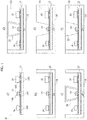
Figure 1 , including portions denoted with letters from a) to f), shows steps of a method according to embodiments, -
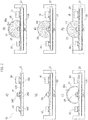
Figure 2 , including portions denoted with letters from a) to f), shows steps of a method according to embodiments, and -
Figure 3 , including portions denoted with letters from a) to e), shows steps of a method according to embodiments. - It will be appreciated that, for clarity and simplicity of illustration, the various parts and components shown in the Figures may not be drawn to scale.
- In the following description, various specific details are given to provide a thorough understanding of various exemplary embodiments of the present specification. The embodiments may be practiced without one or several specific details, or with other methods, components, materials, etc. In other instances, well-known structures, materials or operations are not shown or described in detail to avoid obscuring various aspects of the embodiments.
- Reference throughout this specification to "one embodiment" or "an embodiment" means that a particular feature, structure, or characteristic described in connection with the embodiment is included in at least one embodiment. Thus, the possible appearances of the phrases "in one embodiment" or "in an embodiment" in various places throughout this specification are not necessarily all referring to the same embodiment. Furthermore, particular features, structures, or characteristics may be combined in any suitable manner in one or more embodiments.
- The headings provided herein are for convenience only, and therefore do not interpret the extent of protection or scope of the embodiments.
- One or more embodiments propose various solutions for producing flexible protected modules, e.g. LED modules, wherein only the LEDs are visible from the outside. Moreover, the conditions of low thermal colour shift are promoted.
- One or more embodiments may e.g. envisage:
- the selective deposition of a light-coloured elastomer material (e.g. white silicone) onto a support such as a Flexible Printed Circuit (FPC), only covering the associated electrical/electronic circuitry without touching the LEDs,
- a selective deposition of a transparent elastomer material (e.g. silicone) onto the LEDs, and
- resorting to a special material composition and/or structure for the transparent elastomer which is adapted to enclose the LEDs.
- One or more embodiments may envisage the use of an elongate, e.g. ribbon-shaped, flexible lighting module, denoted as 10 and shown in the annexed Figures in cross section.
- As regards the present specification, said
module 10 may be considered as an element of indeterminate length, optionally adapted to be cut to length according to the application and usage needs. - According to criteria known in themselves (which makes it unnecessary to provide a detailed description thereof), said
module 10 may include (in this respect, see e.g. the portion denoted as a) inFigures 1 ,2 and3 ) : - an elongate, e.g. ribbon-shaped, and flexible substrate or
support 12, which may include e.g. a Flexible Printed Circuit (FPC), with electricallyconductive lines 120 provided e.g. on the front face (above in the Figures) ofsubstrate 12, - one or more electrically-powered
light radiation sources 14, adapted to include solid-state light radiation sources such as e.g. LED sources, optionally with alens 140 associated thereto, and - one or more electrical and/or
electronic circuit components 16 coupled to thelight radiation sources 14 through the electricallyconductive lines 120, having a supply and/or driving function. - In portion a) of
Figures 1 ,2 and3 ,reference 160 denotes electrical junctions (e.g. soldering) between the electricallyconductive lines 120 and theLEDs 14 and/or thecircuitry 16 which, in one or more embodiments, may be mounted onto support orsubstrate 12 via an SMT mounting process. - For simplicity of illustration, in the remaining portions of
Figures 1 ,2 and3 , the only components ofmodule 10 which are shown are thesupport 12, the light radiation source(s) 14 and thecircuitry 16. - In the Figures,
reference 18 denotes a generally channel-shaped housing or casing, including e.g. an elastomer material: this may be e.g. a white-coloured silicone elastomer. -
Housing 18 is destined tohost module 10 therein, with the possible application of one or more masses of sealing material (20 and 22 in the Figures) adapted to impart protection features against the penetration of external agents (e.g. an IP degree protection) to the lighting device. - One or more embodiments may envisage the use of a
first material 20, e.g. a light-coloured elastomer (having any reflection index), generally light-impermeable, destined to be deposited into the channel profile ofhousing 18, with the exception of the area or region wherein the light radiation source(s) 14 are located. - In one or more embodiments, said area or region is adapted to be filled with a light-
permeable material 22, e.g. a transparent elastomer, and/or to embed light-diffusive particles. - In one or more embodiments,
elastomer 22 may have a reflection index matched to the reflection index oflens 140, optionally provided on the light radiation source(s) 14. - For example, in one or more embodiments,
module 10 may be arranged withinhousing 18 as exemplified in portion b) ofFigures 1 to 3 , and it may be fixed in that position through anadhesive layer 24. - Starting from the portion denoted as c),
Figures 1 to 3 exemplify possible embodiments adapted to differ in one or more features: the presence of a certain feature exemplified in one of theFigures 1 to 3 does not exclude the application of that same feature in one or more embodiments exemplified in other Figures. - In one or more embodiments as exemplified in portion c) of
Figure 1 , around the or eachlight radiation source 14 there may be provided a protective shell orscreen 26, e.g. of a non-stick material. - In one or more embodiments, shell or
screen 26 may have a hollow shape (so that it may contain an aeriform mass surrounding source 14). - In one or more embodiments, a shell or
screen 26 may be chosen having a flared shape, e.g. the shape of a truncated cone flaring in the direction away fromsource 14. - In one or more embodiments,
shell 26 may have a height, orthogonally to the bottom plane ofhousing 18, approximatively equal or optionally superior to the corresponding dimension (again, the "height") of the side walls ofhousing 18. - As exemplified in portion d) of
Figure 1 , in one or more embodiments the sealingmaterial 20 may be introduced intohousing 18 so that it covers components 16 (which are assumed as being dark, e.g. black), so that the latter components are masked from the outside thanks to the generally light-coloured, e.g. white, sealingmass 20. - In a step exemplified in portion e) of
Figure 1 , shell orscreen 26 may be removed (this operation may be made easier by the optional non-stick properties of the material of shell 26), and this may be followed by the introduction of the second sealingmass 22 in the position occupied by source(s) 14, i.e. in the portion of the inner cavity ofhousing 18 from which screen 26 has been removed and which now is uncovered. -
Mass 22 may complete the sealing, i.e. the protection of the device against the penetration of foreign agents; because it is light-permeable (e.g. including a transparent silicone material),mass 22 may achieve said sealing/protection effect without hampering the propagation of the light radiation output from the source(s) 14 in operation. - In one or more embodiments, sealing
masses - This may take place via subsequent treatments, carried out either in discrete ways and times for
mass 20 andmass 22, or in a single combined curing of bothmaterials - In one or more embodiments, as exemplified in
Figure 2 (wherein parts and elements corresponding to parts and elements previously described with reference toFigure 1 are denoted by the same references, therefore making it unnecessary to repeat a detailed description thereof), the filling ofhousing 18 with sealing masses 20 (light-impermeable) and 22 (light-permeable) may take place in a so to say inverted sequence with respect to what is exemplified inFigure 1 . - In the embodiments exemplified in
Figure 2 , oncemodule 10 is arranged in housing 18 (see portions a) and b) ofFigure 2 ), on the light radiation source (s) 14 there may be arranged a shell orscreen 26, once again adapted to be hollow, so as to form e.g. a dome to protect source(s) 14. - In one or more embodiments, shell or
screen 26 may be provided with at least oneinjection nozzle 26a, through which (see e.g. the sequence of portions c) and d) ofFigure 2 ) the light-permeable sealing mass 22 may be injected, so as to fill the internal space ofshell 26 above source(s) 14. - In one or more embodiments, shell or
screen 26 may be comprised of a non-stick material, so as to favour the removal of screen 26 (see portion e) ofFigure 2 ), so that around source(s) 14 it is possible to preserve a mass of light-permeable sealing material 22. - In one or more embodiments,
material 22 does not hamper the propagation of the light radiation emitted by source (s) 14. At the same time, material 22 (which may optionally be already cured) may protect source(s) 14 when the sealingmass 20 is introduced intohousing 18, as exemplified in portion f) ofFigure 2 . - Also in this case, the sealing mass 20 (which may be cured) forms a masking layer which hides the
circuit components 16 from the outside. Moreover, the light-permeable mass 22 allows the light radiation output from source(s) 14 to propagate towards the outside. - In this case,
mass 20 may round off the sealing, i.e. the protection of the device from penetration of external agents and in addition, because it is light-impermeable (e.g. because it is comprised of white silicone material), it may maskcomponents 16 from the outside. - In one or more embodiments, sealing
masses mass 22 and formass 20, or in one combined curing step of bothmaterials - As exemplified in
Figure 2 , in one or more embodiments shell 26 may be chosen with such dimensions that the mass ofmaterial 22 formed therein has a "height" superior to the height of the side walls ofhousing 18, so thatmass 22 forms a dome projecting from the plane of the maskingmass 20, the possibility being given (for mass 22) of performing an optical shaping action on the light radiation beam emitted by source(s) 14. - In one or more embodiments, as exemplified in
Figure 3 (wherein, once again, parts or elements corresponding to parts or elements already described with reference toFigures 1 and2 are denoted with the same references, which makes it unnecessary to repeat a corresponding detailed description) shell orscreen 26 may instead be left in position. - To this end, in one or more embodiments, once
module 10 has been arranged within housing 18 (portions a) and b) ofFigure 3 ), around source(s) there may be arranged afixing line 26b, e.g. of an adhesive material, so as to enable the fixation onmodule 10 of shell orscreen 26, which is adapted to include a light-permeable material. - In one or more embodiments, screen or
shell 26 may be imparted with optical properties, e.g. the features of a lens adapted to shape the light radiation beam emitted by source(s) 14. - In one or more embodiments, fixing shell or
screen 26 may be achieved via a slight pressure exerted during mounting and/or thanks to curingline 26b, which may include e.g. curable adhesive material. - After positioning screen 26 (portion d) of
Figure 3 ) it is possible to apply the light-impermeable sealing mass denoted as 20, adapted to perform a masking function ofcomponents 16. - In one or more embodiments as exemplified in
Figure 3 , it is possible to perform one single curing step of material 20 (which may optionally lead to curingline 26b as well). - In one or more embodiments,
mass 20 is adapted to perform, in combination withshell 26 left in place, the function of protectingdevice 10 from external agents. Because it is light-impermeable (e.g. because it includes white silicone material),mass 20 may moreover perform a masking action ofcomponents 16 from the outside. - Said effect of sealing/protection may be achieved without hampering the propagation of the light radiation emitted by source(s) 14 in operation, because source(s) 14 are located within shell or
screen 26, which is light-permeable. - One or more embodiments may therefore concern a method of producing lighting devices, the method including:
- providing a channel-shaped housing (e.g. 18),
- arranging in said housing a lighting module (e.g. 10) with at least one electrically-powered light radiation source (e.g. 14) and circuitry (e.g. 16) coupled (e.g. through lines 120) with said at least one light radiation source, said at least one light radiation source and said circuitry facing towards the opening of the channel-shaped housing,
- providing a light-permeable cover (e.g. 22, 26) that covers said at least one light radiation source and leaves said circuitry uncovered, and
- providing a sealing mass of light-impermeable material (e.g. 20) in said channel-shaped housing, said sealing mass masking said circuitry, with the light radiation emitted from said at least one light radiation source being adapted to propagate through said light-permeable cover.
- One or more embodiments may include:
- providing a temporary screen (e.g. 26) covering said at least one light radiation source and leaving said circuitry uncovered,
- providing said sealing mass of light-impermeable material with said at least one light radiation source covered by said temporary screen,
- removing said temporary screen, and
- filling the free space resulting from removing said temporary screen with a filling of light-permeable material.
- One or more embodiments may include:
- providing a temporary screen covering said at least one light radiation source and leaving said circuitry uncovered, said temporary screen including a hollow body,
- injecting (e.g. 26a) into said hollow body light-permeable material, thus providing a light-permeable cover that covers said at least one light radiation source and leaves said circuitry uncovered, and
- removing said temporary screen after injecting said light-permeable material into said hollow body.
- In one or more embodiments, said light-permeable cover may include a hollow body of light-permeable material which encloses said at least one light radiation source, optionally leaving a space around said at least one light radiation source.
- One or more embodiments may include providing said sealing mass of light-impermeable material by sealingly enclosing said light-permeable cover that covers said at least one light radiation source.
- In one or more embodiments:
- said at least one electrically-powered light radiation source may include a LED source, and/or
- with said at least one electrically-powered light radiation source there may be associated a lens (e.g. 140), with said light-permeable cover having a reflection coefficient matched to the reflection coefficient of said lens.
- In one or more embodiments, a lighting device may include:
- a channel-shaped housing,
- a lighting module arranged in said channel-shaped housing, said lighting module (10) having at least one electrically-powered light radiation source and circuitry coupled with said at least one light radiation source, the at least one light radiation source and the circuitry facing towards the opening of the channel shape of the housing,
- a light-permeable cover that covers said at least one light radiation source and leaves said circuitry uncovered, and
- a sealing mass of light-impermeable material that covers said circuitry, wherein said circuitry is masked by said light-impermeable material.
- In one or more embodiments, said light-permeable cover may include light-permeable material introduced (e.g. 26a) into said channel-shaped housing.
- In one or more embodiments, said light-permeable cover may include a body of light-permeable material that encloses said at least one light radiation source, optionally leaving a space around said light radiation source.
- In one or more embodiments:
- said at least one electrically powered light radiation source may include a LED source, and/or
- with said at least one electrically powered light radiation source there may be associated a lens, with said light-permeable cover having a reflection coefficient matched to the reflection coefficient of said lens.
- Without prejudice to the basic principles, the details and the embodiments may vary, even appreciably, with respect to what has been described herein by way of non-limiting example only, without departing from the extent of protection.
- The extent of protection is defined by the annexed claims.
Claims (10)
- A method of producing lighting devices, the method including:- providing a channel-shaped housing (18),- arranging in said housing (18) a lighting module (10) with at least one electrically-powered light radiation source (14) and circuitry (16) coupled (120) with said at least one light radiation source (14), said at least one light radiation source (14) and said circuitry (16) facing towards the opening of the channel-shaped housing (12),- providing a light-permeable cover (22, 26) that covers said at least one light radiation source (14) and leaves said circuitry (16) uncovered, and- providing a sealing mass of light-impermeable material (20) in said channel-shaped housing (18), said sealing mass (20) masking said circuitry (16) with the light radiation from said at least one light radiation source (14) propagating through said light permeable cover (22, 26).
- The method of claim 1, including:- providing a temporary shield (26) covering said at least one light radiation source (14) and leaving said circuitry uncovered (16),- providing said sealing mass of light-impermeable material (20) with said at least one light radiation source (14) covered by said temporary shield (26),- removing said temporary shield (26), and- filling the free space resulting from removing said temporary screen (26) with a filling of light-permeable material (22).
- The method of claim 1, including:- providing a temporary shield (26) covering said at least one light radiation source (14) and leaving said circuitry uncovered (16), said temporary shield (26) including a hollow body,- injecting (26a) into said hollow body (26) light permeable material (22) providing a light-permeable cover that covers said at least one light radiation source (14) and leaves said circuitry (16) uncovered, and- removing said temporary shield (26) after injecting (26a) said light permeable material (22) into said hollow body.
- The method of claim 1, wherein said light-permeable cover includes a hollow body (26) of light-permeable material which encloses said at least one light radiation source (14), preferably by leaving a space around said at least one light radiation source (14).
- The method of any of the preceding claims, including providing said sealing mass of light-impermeable material (20) by sealingly enclosing said light-permeable cover (22, 26) that covers said at least one light radiation source (14).
- The method of any of the preceding claims, wherein:- said at least one electrically powered light radiation source (14) includes a LED light source, and/or- with said at least one electrically powered light radiation source (14) there is associated a lens (140) with said light-permeable cover (22) having a reflection coefficient matched to the reflection coefficient of said lens (140).
- A lighting device, including:- a channel-shaped housing (18),- a lighting module (10) arranged in said channel-shaped housing (18), said lighting module (10) with at least one electrically-powered light radiation source (14) and circuitry (16) coupled with said at least one light radiation source (14), the at least one light radiation source (14) and the circuitry (16) facing towards the opening of the channel shape of the housing (18),- a light-permeable cover (22, 26) that covers said at least one light radiation source (14) and leaves said circuitry (16) uncovered, and- a sealing mass of light-impermeable material (20) that covers said circuitry (16), wherein said circuitry (16) is masked by said light-impermeable material.
- The lighting device of claim 7, wherein said light-permeable cover includes light-permeable material (22) input (26a) into said channel-shaped housing.
- The lighting device of claim 7, wherein said light-permeable cover includes a body (26) of light-permeable material that encloses said at least one light radiation source (14), preferably by leaving a space around said light radiation source (14).
- The lighting device of any of claims 7 to 9, wherein:- said at least one electrically powered light radiation source (14) includes a LED light source, and/or- with said at least one electrically powered light radiation source (14) there is associated a lens (140) with said light-permeable cover (22) having a reflection coefficient matched to the reflection coefficient of said lens (140).
Applications Claiming Priority (1)
| Application Number | Priority Date | Filing Date | Title |
|---|---|---|---|
| ITUA20164709 | 2016-06-28 |
Publications (2)
| Publication Number | Publication Date |
|---|---|
| EP3263983A1 true EP3263983A1 (en) | 2018-01-03 |
| EP3263983B1 EP3263983B1 (en) | 2019-05-15 |
Family
ID=57750423
Family Applications (1)
| Application Number | Title | Priority Date | Filing Date |
|---|---|---|---|
| EP17177797.2A Active EP3263983B1 (en) | 2016-06-28 | 2017-06-26 | A method of producing lighting devices and corresponding device |
Country Status (1)
| Country | Link |
|---|---|
| EP (1) | EP3263983B1 (en) |
Cited By (2)
| Publication number | Priority date | Publication date | Assignee | Title |
|---|---|---|---|---|
| EP3431862A1 (en) * | 2017-07-21 | 2019-01-23 | OSRAM GmbH | A method for manufacturing a lighting device and corresponding device |
| EP3821168A1 (en) * | 2018-07-09 | 2021-05-19 | Linxens Holding | Flexible luminous device |
Citations (6)
| Publication number | Priority date | Publication date | Assignee | Title |
|---|---|---|---|---|
| US6505955B1 (en) * | 1996-11-25 | 2003-01-14 | Oy Modular Technology Group Engineering Ltd. | Method for production of conducting element and conducting element |
| JP2009194026A (en) * | 2008-02-12 | 2009-08-27 | Stanley Electric Co Ltd | Light emitting device and manufacturing method thereof |
| US20100142180A1 (en) * | 2009-03-24 | 2010-06-10 | Bridgelux, Inc. | Light emitting diode source with protective barrier |
| DE102012222093A1 (en) * | 2012-12-03 | 2014-06-05 | Osram Gmbh | Lighting device e.g. LED module has conversion transparent protective cover which is covered on light-emitting surface in which translucent diffusing layer is arranged with translucent matrix material having scattering particles |
| EP2892078A1 (en) * | 2013-12-30 | 2015-07-08 | OSRAM GmbH | A lighting device and corresponding method |
| US20150338080A1 (en) * | 2014-05-22 | 2015-11-26 | Moore Holding Group, LLC | Rugged light assembly having improved resiliency and method for making the same |
-
2017
- 2017-06-26 EP EP17177797.2A patent/EP3263983B1/en active Active
Patent Citations (6)
| Publication number | Priority date | Publication date | Assignee | Title |
|---|---|---|---|---|
| US6505955B1 (en) * | 1996-11-25 | 2003-01-14 | Oy Modular Technology Group Engineering Ltd. | Method for production of conducting element and conducting element |
| JP2009194026A (en) * | 2008-02-12 | 2009-08-27 | Stanley Electric Co Ltd | Light emitting device and manufacturing method thereof |
| US20100142180A1 (en) * | 2009-03-24 | 2010-06-10 | Bridgelux, Inc. | Light emitting diode source with protective barrier |
| DE102012222093A1 (en) * | 2012-12-03 | 2014-06-05 | Osram Gmbh | Lighting device e.g. LED module has conversion transparent protective cover which is covered on light-emitting surface in which translucent diffusing layer is arranged with translucent matrix material having scattering particles |
| EP2892078A1 (en) * | 2013-12-30 | 2015-07-08 | OSRAM GmbH | A lighting device and corresponding method |
| US20150338080A1 (en) * | 2014-05-22 | 2015-11-26 | Moore Holding Group, LLC | Rugged light assembly having improved resiliency and method for making the same |
Cited By (2)
| Publication number | Priority date | Publication date | Assignee | Title |
|---|---|---|---|---|
| EP3431862A1 (en) * | 2017-07-21 | 2019-01-23 | OSRAM GmbH | A method for manufacturing a lighting device and corresponding device |
| EP3821168A1 (en) * | 2018-07-09 | 2021-05-19 | Linxens Holding | Flexible luminous device |
Also Published As
| Publication number | Publication date |
|---|---|
| EP3263983B1 (en) | 2019-05-15 |
Similar Documents
| Publication | Publication Date | Title |
|---|---|---|
| US6988819B2 (en) | Lamp housing containing an integrated LED support structure | |
| CN106016121A (en) | Light source unit, method of manufacturing the same, and vehicle lamp | |
| US9324928B2 (en) | Lighting device and corresponding method | |
| RU2011134605A (en) | LAMP CAP AND LED LAMP WITH SUCH CAP | |
| JP2015222832A (en) | Explosion-proof led module | |
| JP2010524269A5 (en) | ||
| CN102270414A (en) | Display apparatus and method for producing the same | |
| EP3263983B1 (en) | A method of producing lighting devices and corresponding device | |
| US20210270429A1 (en) | Light string package structure | |
| US20160334090A1 (en) | Connector for lighting devices and corresponding method | |
| CN107013814B (en) | LED signal module | |
| KR100746598B1 (en) | LED display board and manufacturing method thereof | |
| CN106716005A (en) | Substrate for a light module with metal strip used as shielding, a heat screen and/or an optical reflector | |
| CN109417116A (en) | LED lamp system | |
| JP6541444B2 (en) | Display device and display unit | |
| WO2015190431A1 (en) | Led unit | |
| TW200603448A (en) | Optical communication module | |
| EP3404317B1 (en) | A lighting device and corresponding method | |
| CN107611243B (en) | Display unit and display device | |
| NL2028757B1 (en) | Explosion safe illumination unit and method for manufacturing an explosion safe illumination unit | |
| KR102394587B1 (en) | Multiple structure of In-mold electronics and method producing the same | |
| CN111758168B (en) | Sealed device with light engine | |
| JP2011193033A (en) | Infrared data communication module | |
| US20160126430A1 (en) | Light-emitting device with hardened encapsulant islands | |
| US12317656B2 (en) | Light emitting device |
Legal Events
| Date | Code | Title | Description |
|---|---|---|---|
| PUAI | Public reference made under article 153(3) epc to a published international application that has entered the european phase |
Free format text: ORIGINAL CODE: 0009012 |
|
| STAA | Information on the status of an ep patent application or granted ep patent |
Free format text: STATUS: THE APPLICATION HAS BEEN PUBLISHED |
|
| AK | Designated contracting states |
Kind code of ref document: A1 Designated state(s): AL AT BE BG CH CY CZ DE DK EE ES FI FR GB GR HR HU IE IS IT LI LT LU LV MC MK MT NL NO PL PT RO RS SE SI SK SM TR |
|
| AX | Request for extension of the european patent |
Extension state: BA ME |
|
| RAP1 | Party data changed (applicant data changed or rights of an application transferred) |
Owner name: OSRAM S.P.A. - SOCIETA' RIUNITE OSRAM EDISON CLERI Owner name: OSRAM GMBH |
|
| STAA | Information on the status of an ep patent application or granted ep patent |
Free format text: STATUS: REQUEST FOR EXAMINATION WAS MADE |
|
| 17P | Request for examination filed |
Effective date: 20180625 |
|
| RBV | Designated contracting states (corrected) |
Designated state(s): AL AT BE BG CH CY CZ DE DK EE ES FI FR GB GR HR HU IE IS IT LI LT LU LV MC MK MT NL NO PL PT RO RS SE SI SK SM TR |
|
| GRAP | Despatch of communication of intention to grant a patent |
Free format text: ORIGINAL CODE: EPIDOSNIGR1 |
|
| STAA | Information on the status of an ep patent application or granted ep patent |
Free format text: STATUS: GRANT OF PATENT IS INTENDED |
|
| RIC1 | Information provided on ipc code assigned before grant |
Ipc: F21Y 103/10 20160101ALN20180921BHEP Ipc: F21S 4/22 20160101ALI20180921BHEP Ipc: F21V 15/01 20060101ALN20180921BHEP Ipc: F21Y 107/70 20160101ALN20180921BHEP Ipc: F21V 23/00 20150101ALN20180921BHEP Ipc: F21V 31/04 20060101AFI20180921BHEP Ipc: F21K 9/90 20160101ALI20180921BHEP Ipc: F21Y 115/10 20160101ALN20180921BHEP |
|
| INTG | Intention to grant announced |
Effective date: 20181026 |
|
| RAP1 | Party data changed (applicant data changed or rights of an application transferred) |
Owner name: OSRAM S.P.A. - SOCIETA' RIUNITE OSRAM EDISON CLERI Owner name: OSRAM GMBH |
|
| GRAS | Grant fee paid |
Free format text: ORIGINAL CODE: EPIDOSNIGR3 |
|
| GRAJ | Information related to disapproval of communication of intention to grant by the applicant or resumption of examination proceedings by the epo deleted |
Free format text: ORIGINAL CODE: EPIDOSDIGR1 |
|
| GRAL | Information related to payment of fee for publishing/printing deleted |
Free format text: ORIGINAL CODE: EPIDOSDIGR3 |
|
| STAA | Information on the status of an ep patent application or granted ep patent |
Free format text: STATUS: REQUEST FOR EXAMINATION WAS MADE |
|
| GRAP | Despatch of communication of intention to grant a patent |
Free format text: ORIGINAL CODE: EPIDOSNIGR1 |
|
| STAA | Information on the status of an ep patent application or granted ep patent |
Free format text: STATUS: GRANT OF PATENT IS INTENDED |
|
| INTC | Intention to grant announced (deleted) | ||
| RIC1 | Information provided on ipc code assigned before grant |
Ipc: F21K 9/90 20160101ALI20190221BHEP Ipc: F21V 23/00 20150101ALN20190221BHEP Ipc: F21Y 103/10 20160101ALN20190221BHEP Ipc: F21Y 107/70 20160101ALN20190221BHEP Ipc: F21V 15/01 20060101ALN20190221BHEP Ipc: F21S 4/22 20160101ALI20190221BHEP Ipc: F21Y 115/10 20160101ALN20190221BHEP Ipc: F21V 31/04 20060101AFI20190221BHEP |
|
| INTG | Intention to grant announced |
Effective date: 20190305 |
|
| RIC1 | Information provided on ipc code assigned before grant |
Ipc: F21Y 107/70 20160101ALN20190225BHEP Ipc: F21V 31/04 20060101AFI20190225BHEP Ipc: F21K 9/90 20160101ALI20190225BHEP Ipc: F21Y 115/10 20160101ALN20190225BHEP Ipc: F21Y 103/10 20160101ALN20190225BHEP Ipc: F21V 15/01 20060101ALN20190225BHEP Ipc: F21V 23/00 20150101ALN20190225BHEP Ipc: F21S 4/22 20160101ALI20190225BHEP |
|
| GRAA | (expected) grant |
Free format text: ORIGINAL CODE: 0009210 |
|
| STAA | Information on the status of an ep patent application or granted ep patent |
Free format text: STATUS: THE PATENT HAS BEEN GRANTED |
|
| AK | Designated contracting states |
Kind code of ref document: B1 Designated state(s): AL AT BE BG CH CY CZ DE DK EE ES FI FR GB GR HR HU IE IS IT LI LT LU LV MC MK MT NL NO PL PT RO RS SE SI SK SM TR |
|
| REG | Reference to a national code |
Ref country code: CH Ref legal event code: EP |
|
| REG | Reference to a national code |
Ref country code: IE Ref legal event code: FG4D |
|
| REG | Reference to a national code |
Ref country code: DE Ref legal event code: R096 Ref document number: 602017003838 Country of ref document: DE |
|
| REG | Reference to a national code |
Ref country code: NL Ref legal event code: MP Effective date: 20190515 |
|
| REG | Reference to a national code |
Ref country code: LT Ref legal event code: MG4D |
|
| PG25 | Lapsed in a contracting state [announced via postgrant information from national office to epo] |
Ref country code: NL Free format text: LAPSE BECAUSE OF FAILURE TO SUBMIT A TRANSLATION OF THE DESCRIPTION OR TO PAY THE FEE WITHIN THE PRESCRIBED TIME-LIMIT Effective date: 20190515 Ref country code: HR Free format text: LAPSE BECAUSE OF FAILURE TO SUBMIT A TRANSLATION OF THE DESCRIPTION OR TO PAY THE FEE WITHIN THE PRESCRIBED TIME-LIMIT Effective date: 20190515 Ref country code: SE Free format text: LAPSE BECAUSE OF FAILURE TO SUBMIT A TRANSLATION OF THE DESCRIPTION OR TO PAY THE FEE WITHIN THE PRESCRIBED TIME-LIMIT Effective date: 20190515 Ref country code: PT Free format text: LAPSE BECAUSE OF FAILURE TO SUBMIT A TRANSLATION OF THE DESCRIPTION OR TO PAY THE FEE WITHIN THE PRESCRIBED TIME-LIMIT Effective date: 20190915 Ref country code: NO Free format text: LAPSE BECAUSE OF FAILURE TO SUBMIT A TRANSLATION OF THE DESCRIPTION OR TO PAY THE FEE WITHIN THE PRESCRIBED TIME-LIMIT Effective date: 20190815 Ref country code: AL Free format text: LAPSE BECAUSE OF FAILURE TO SUBMIT A TRANSLATION OF THE DESCRIPTION OR TO PAY THE FEE WITHIN THE PRESCRIBED TIME-LIMIT Effective date: 20190515 Ref country code: FI Free format text: LAPSE BECAUSE OF FAILURE TO SUBMIT A TRANSLATION OF THE DESCRIPTION OR TO PAY THE FEE WITHIN THE PRESCRIBED TIME-LIMIT Effective date: 20190515 Ref country code: LT Free format text: LAPSE BECAUSE OF FAILURE TO SUBMIT A TRANSLATION OF THE DESCRIPTION OR TO PAY THE FEE WITHIN THE PRESCRIBED TIME-LIMIT Effective date: 20190515 |
|
| PG25 | Lapsed in a contracting state [announced via postgrant information from national office to epo] |
Ref country code: BG Free format text: LAPSE BECAUSE OF FAILURE TO SUBMIT A TRANSLATION OF THE DESCRIPTION OR TO PAY THE FEE WITHIN THE PRESCRIBED TIME-LIMIT Effective date: 20190815 Ref country code: GR Free format text: LAPSE BECAUSE OF FAILURE TO SUBMIT A TRANSLATION OF THE DESCRIPTION OR TO PAY THE FEE WITHIN THE PRESCRIBED TIME-LIMIT Effective date: 20190816 Ref country code: RS Free format text: LAPSE BECAUSE OF FAILURE TO SUBMIT A TRANSLATION OF THE DESCRIPTION OR TO PAY THE FEE WITHIN THE PRESCRIBED TIME-LIMIT Effective date: 20190515 Ref country code: LV Free format text: LAPSE BECAUSE OF FAILURE TO SUBMIT A TRANSLATION OF THE DESCRIPTION OR TO PAY THE FEE WITHIN THE PRESCRIBED TIME-LIMIT Effective date: 20190515 |
|
| REG | Reference to a national code |
Ref country code: AT Ref legal event code: MK05 Ref document number: 1133868 Country of ref document: AT Kind code of ref document: T Effective date: 20190515 |
|
| PG25 | Lapsed in a contracting state [announced via postgrant information from national office to epo] |
Ref country code: DK Free format text: LAPSE BECAUSE OF FAILURE TO SUBMIT A TRANSLATION OF THE DESCRIPTION OR TO PAY THE FEE WITHIN THE PRESCRIBED TIME-LIMIT Effective date: 20190515 Ref country code: AT Free format text: LAPSE BECAUSE OF FAILURE TO SUBMIT A TRANSLATION OF THE DESCRIPTION OR TO PAY THE FEE WITHIN THE PRESCRIBED TIME-LIMIT Effective date: 20190515 Ref country code: EE Free format text: LAPSE BECAUSE OF FAILURE TO SUBMIT A TRANSLATION OF THE DESCRIPTION OR TO PAY THE FEE WITHIN THE PRESCRIBED TIME-LIMIT Effective date: 20190515 Ref country code: CZ Free format text: LAPSE BECAUSE OF FAILURE TO SUBMIT A TRANSLATION OF THE DESCRIPTION OR TO PAY THE FEE WITHIN THE PRESCRIBED TIME-LIMIT Effective date: 20190515 Ref country code: SK Free format text: LAPSE BECAUSE OF FAILURE TO SUBMIT A TRANSLATION OF THE DESCRIPTION OR TO PAY THE FEE WITHIN THE PRESCRIBED TIME-LIMIT Effective date: 20190515 |
|
| REG | Reference to a national code |
Ref country code: DE Ref legal event code: R097 Ref document number: 602017003838 Country of ref document: DE |
|
| PG25 | Lapsed in a contracting state [announced via postgrant information from national office to epo] |
Ref country code: SM Free format text: LAPSE BECAUSE OF FAILURE TO SUBMIT A TRANSLATION OF THE DESCRIPTION OR TO PAY THE FEE WITHIN THE PRESCRIBED TIME-LIMIT Effective date: 20190515 Ref country code: MC Free format text: LAPSE BECAUSE OF FAILURE TO SUBMIT A TRANSLATION OF THE DESCRIPTION OR TO PAY THE FEE WITHIN THE PRESCRIBED TIME-LIMIT Effective date: 20190515 Ref country code: IT Free format text: LAPSE BECAUSE OF FAILURE TO SUBMIT A TRANSLATION OF THE DESCRIPTION OR TO PAY THE FEE WITHIN THE PRESCRIBED TIME-LIMIT Effective date: 20190515 |
|
| PLBE | No opposition filed within time limit |
Free format text: ORIGINAL CODE: 0009261 |
|
| STAA | Information on the status of an ep patent application or granted ep patent |
Free format text: STATUS: NO OPPOSITION FILED WITHIN TIME LIMIT |
|
| REG | Reference to a national code |
Ref country code: BE Ref legal event code: MM Effective date: 20190630 |
|
| PG25 | Lapsed in a contracting state [announced via postgrant information from national office to epo] |
Ref country code: TR Free format text: LAPSE BECAUSE OF FAILURE TO SUBMIT A TRANSLATION OF THE DESCRIPTION OR TO PAY THE FEE WITHIN THE PRESCRIBED TIME-LIMIT Effective date: 20190515 |
|
| 26N | No opposition filed |
Effective date: 20200218 |
|
| PG25 | Lapsed in a contracting state [announced via postgrant information from national office to epo] |
Ref country code: PL Free format text: LAPSE BECAUSE OF FAILURE TO SUBMIT A TRANSLATION OF THE DESCRIPTION OR TO PAY THE FEE WITHIN THE PRESCRIBED TIME-LIMIT Effective date: 20190515 Ref country code: IE Free format text: LAPSE BECAUSE OF NON-PAYMENT OF DUE FEES Effective date: 20190626 |
|
| PG25 | Lapsed in a contracting state [announced via postgrant information from national office to epo] |
Ref country code: SI Free format text: LAPSE BECAUSE OF FAILURE TO SUBMIT A TRANSLATION OF THE DESCRIPTION OR TO PAY THE FEE WITHIN THE PRESCRIBED TIME-LIMIT Effective date: 20190515 Ref country code: LU Free format text: LAPSE BECAUSE OF NON-PAYMENT OF DUE FEES Effective date: 20190626 Ref country code: BE Free format text: LAPSE BECAUSE OF NON-PAYMENT OF DUE FEES Effective date: 20190630 |
|
| PG25 | Lapsed in a contracting state [announced via postgrant information from national office to epo] |
Ref country code: FR Free format text: LAPSE BECAUSE OF NON-PAYMENT OF DUE FEES Effective date: 20190715 |
|
| PG25 | Lapsed in a contracting state [announced via postgrant information from national office to epo] |
Ref country code: ES Free format text: LAPSE BECAUSE OF FAILURE TO SUBMIT A TRANSLATION OF THE DESCRIPTION OR TO PAY THE FEE WITHIN THE PRESCRIBED TIME-LIMIT Effective date: 20190515 |
|
| REG | Reference to a national code |
Ref country code: CH Ref legal event code: PL |
|
| PG25 | Lapsed in a contracting state [announced via postgrant information from national office to epo] |
Ref country code: LI Free format text: LAPSE BECAUSE OF NON-PAYMENT OF DUE FEES Effective date: 20200630 Ref country code: CH Free format text: LAPSE BECAUSE OF NON-PAYMENT OF DUE FEES Effective date: 20200630 Ref country code: RO Free format text: LAPSE BECAUSE OF FAILURE TO SUBMIT A TRANSLATION OF THE DESCRIPTION OR TO PAY THE FEE WITHIN THE PRESCRIBED TIME-LIMIT Effective date: 20190515 |
|
| PG25 | Lapsed in a contracting state [announced via postgrant information from national office to epo] |
Ref country code: CY Free format text: LAPSE BECAUSE OF FAILURE TO SUBMIT A TRANSLATION OF THE DESCRIPTION OR TO PAY THE FEE WITHIN THE PRESCRIBED TIME-LIMIT Effective date: 20190515 |
|
| PG25 | Lapsed in a contracting state [announced via postgrant information from national office to epo] |
Ref country code: IS Free format text: LAPSE BECAUSE OF FAILURE TO SUBMIT A TRANSLATION OF THE DESCRIPTION OR TO PAY THE FEE WITHIN THE PRESCRIBED TIME-LIMIT Effective date: 20190915 |
|
| PG25 | Lapsed in a contracting state [announced via postgrant information from national office to epo] |
Ref country code: MT Free format text: LAPSE BECAUSE OF FAILURE TO SUBMIT A TRANSLATION OF THE DESCRIPTION OR TO PAY THE FEE WITHIN THE PRESCRIBED TIME-LIMIT Effective date: 20190515 Ref country code: HU Free format text: LAPSE BECAUSE OF FAILURE TO SUBMIT A TRANSLATION OF THE DESCRIPTION OR TO PAY THE FEE WITHIN THE PRESCRIBED TIME-LIMIT; INVALID AB INITIO Effective date: 20170626 |
|
| GBPC | Gb: european patent ceased through non-payment of renewal fee |
Effective date: 20210626 |
|
| PG25 | Lapsed in a contracting state [announced via postgrant information from national office to epo] |
Ref country code: GB Free format text: LAPSE BECAUSE OF NON-PAYMENT OF DUE FEES Effective date: 20210626 |
|
| PG25 | Lapsed in a contracting state [announced via postgrant information from national office to epo] |
Ref country code: MK Free format text: LAPSE BECAUSE OF FAILURE TO SUBMIT A TRANSLATION OF THE DESCRIPTION OR TO PAY THE FEE WITHIN THE PRESCRIBED TIME-LIMIT Effective date: 20190515 |
|
| REG | Reference to a national code |
Ref country code: DE Ref legal event code: R081 Ref document number: 602017003838 Country of ref document: DE Owner name: OPTOTRONIC GMBH, DE Free format text: FORMER OWNER: OSRAM GMBH, 80807 MUENCHEN, DE Ref country code: DE Ref legal event code: R081 Ref document number: 602017003838 Country of ref document: DE Owner name: INVENTRONICS GMBH, DE Free format text: FORMER OWNER: OSRAM GMBH, 80807 MUENCHEN, DE |
|
| REG | Reference to a national code |
Ref country code: DE Ref legal event code: R081 Ref document number: 602017003838 Country of ref document: DE Owner name: INVENTRONICS GMBH, DE Free format text: FORMER OWNER: OPTOTRONIC GMBH, 85748 GARCHING, DE |
|
| PGFP | Annual fee paid to national office [announced via postgrant information from national office to epo] |
Ref country code: DE Payment date: 20250618 Year of fee payment: 9 |