EP3263517A1 - Mems device formed by at least two bonded structural layers and manufacturing process thereof - Google Patents
Mems device formed by at least two bonded structural layers and manufacturing process thereof Download PDFInfo
- Publication number
- EP3263517A1 EP3263517A1 EP16206887.8A EP16206887A EP3263517A1 EP 3263517 A1 EP3263517 A1 EP 3263517A1 EP 16206887 A EP16206887 A EP 16206887A EP 3263517 A1 EP3263517 A1 EP 3263517A1
- Authority
- EP
- European Patent Office
- Prior art keywords
- bonding
- substrate
- face
- recess
- forming
- Prior art date
- Legal status (The legal status is an assumption and is not a legal conclusion. Google has not performed a legal analysis and makes no representation as to the accuracy of the status listed.)
- Withdrawn
Links
- 238000004519 manufacturing process Methods 0.000 title claims description 20
- 239000000758 substrate Substances 0.000 claims abstract description 58
- 239000000463 material Substances 0.000 claims abstract description 40
- 239000004065 semiconductor Substances 0.000 claims abstract description 17
- 238000000151 deposition Methods 0.000 claims abstract description 6
- 238000000034 method Methods 0.000 claims description 23
- 229910052751 metal Inorganic materials 0.000 claims description 12
- 239000002184 metal Substances 0.000 claims description 12
- 230000005496 eutectics Effects 0.000 claims description 8
- 239000011521 glass Substances 0.000 claims description 8
- 229920000642 polymer Polymers 0.000 claims description 5
- 235000012431 wafers Nutrition 0.000 abstract description 89
- 239000010410 layer Substances 0.000 description 36
- 238000005530 etching Methods 0.000 description 9
- 239000000126 substance Substances 0.000 description 6
- KWYUFKZDYYNOTN-UHFFFAOYSA-M Potassium hydroxide Chemical compound [OH-].[K+] KWYUFKZDYYNOTN-UHFFFAOYSA-M 0.000 description 5
- XUIMIQQOPSSXEZ-UHFFFAOYSA-N Silicon Chemical compound [Si] XUIMIQQOPSSXEZ-UHFFFAOYSA-N 0.000 description 5
- 239000002131 composite material Substances 0.000 description 5
- 229910052710 silicon Inorganic materials 0.000 description 5
- 239000010703 silicon Substances 0.000 description 5
- 229910021421 monocrystalline silicon Inorganic materials 0.000 description 4
- 238000001039 wet etching Methods 0.000 description 4
- 229910017401 Au—Ge Inorganic materials 0.000 description 3
- 229910015363 Au—Sn Inorganic materials 0.000 description 3
- 238000004140 cleaning Methods 0.000 description 3
- 239000010931 gold Substances 0.000 description 3
- 229910052737 gold Inorganic materials 0.000 description 3
- 238000005459 micromachining Methods 0.000 description 3
- 229910018459 Al—Ge Inorganic materials 0.000 description 2
- 229910017755 Cu-Sn Inorganic materials 0.000 description 2
- 229910017927 Cu—Sn Inorganic materials 0.000 description 2
- VYPSYNLAJGMNEJ-UHFFFAOYSA-N Silicium dioxide Chemical compound O=[Si]=O VYPSYNLAJGMNEJ-UHFFFAOYSA-N 0.000 description 2
- KUNSUQLRTQLHQQ-UHFFFAOYSA-N copper tin Chemical compound [Cu].[Sn] KUNSUQLRTQLHQQ-UHFFFAOYSA-N 0.000 description 2
- 230000008878 coupling Effects 0.000 description 2
- 238000010168 coupling process Methods 0.000 description 2
- 238000005859 coupling reaction Methods 0.000 description 2
- 238000001312 dry etching Methods 0.000 description 2
- 238000009413 insulation Methods 0.000 description 2
- 238000004518 low pressure chemical vapour deposition Methods 0.000 description 2
- 238000004377 microelectronic Methods 0.000 description 2
- 238000000059 patterning Methods 0.000 description 2
- 238000005240 physical vapour deposition Methods 0.000 description 2
- 238000000623 plasma-assisted chemical vapour deposition Methods 0.000 description 2
- 229910021420 polycrystalline silicon Inorganic materials 0.000 description 2
- 229910052814 silicon oxide Inorganic materials 0.000 description 2
- WGTYBPLFGIVFAS-UHFFFAOYSA-M tetramethylammonium hydroxide Chemical compound [OH-].C[N+](C)(C)C WGTYBPLFGIVFAS-UHFFFAOYSA-M 0.000 description 2
- 239000004642 Polyimide Substances 0.000 description 1
- 239000000853 adhesive Substances 0.000 description 1
- 230000001070 adhesive effect Effects 0.000 description 1
- 230000006835 compression Effects 0.000 description 1
- 238000007906 compression Methods 0.000 description 1
- 238000011109 contamination Methods 0.000 description 1
- 239000003989 dielectric material Substances 0.000 description 1
- 238000004070 electrodeposition Methods 0.000 description 1
- 238000005516 engineering process Methods 0.000 description 1
- PCHJSUWPFVWCPO-UHFFFAOYSA-N gold Chemical compound [Au] PCHJSUWPFVWCPO-UHFFFAOYSA-N 0.000 description 1
- 238000012986 modification Methods 0.000 description 1
- 230000004048 modification Effects 0.000 description 1
- 230000002093 peripheral effect Effects 0.000 description 1
- 229920002120 photoresistant polymer Polymers 0.000 description 1
- 229920001721 polyimide Polymers 0.000 description 1
- 239000011241 protective layer Substances 0.000 description 1
- 238000007789 sealing Methods 0.000 description 1
Images




Classifications
-
- B—PERFORMING OPERATIONS; TRANSPORTING
- B81—MICROSTRUCTURAL TECHNOLOGY
- B81C—PROCESSES OR APPARATUS SPECIALLY ADAPTED FOR THE MANUFACTURE OR TREATMENT OF MICROSTRUCTURAL DEVICES OR SYSTEMS
- B81C1/00—Manufacture or treatment of devices or systems in or on a substrate
- B81C1/00015—Manufacture or treatment of devices or systems in or on a substrate for manufacturing microsystems
- B81C1/00261—Processes for packaging MEMS devices
- B81C1/00269—Bonding of solid lids or wafers to the substrate
-
- B—PERFORMING OPERATIONS; TRANSPORTING
- B81—MICROSTRUCTURAL TECHNOLOGY
- B81B—MICROSTRUCTURAL DEVICES OR SYSTEMS, e.g. MICROMECHANICAL DEVICES
- B81B3/00—Devices comprising flexible or deformable elements, e.g. comprising elastic tongues or membranes
- B81B3/0097—Devices comprising flexible or deformable elements not provided for in groups B81B3/0002 - B81B3/0094
-
- B—PERFORMING OPERATIONS; TRANSPORTING
- B81—MICROSTRUCTURAL TECHNOLOGY
- B81C—PROCESSES OR APPARATUS SPECIALLY ADAPTED FOR THE MANUFACTURE OR TREATMENT OF MICROSTRUCTURAL DEVICES OR SYSTEMS
- B81C3/00—Assembling of devices or systems from individually processed components
- B81C3/001—Bonding of two components
-
- B—PERFORMING OPERATIONS; TRANSPORTING
- B81—MICROSTRUCTURAL TECHNOLOGY
- B81B—MICROSTRUCTURAL DEVICES OR SYSTEMS, e.g. MICROMECHANICAL DEVICES
- B81B2201/00—Specific applications of microelectromechanical systems
- B81B2201/02—Sensors
- B81B2201/0228—Inertial sensors
- B81B2201/0242—Gyroscopes
-
- B—PERFORMING OPERATIONS; TRANSPORTING
- B81—MICROSTRUCTURAL TECHNOLOGY
- B81B—MICROSTRUCTURAL DEVICES OR SYSTEMS, e.g. MICROMECHANICAL DEVICES
- B81B2201/00—Specific applications of microelectromechanical systems
- B81B2201/02—Sensors
- B81B2201/0264—Pressure sensors
-
- B—PERFORMING OPERATIONS; TRANSPORTING
- B81—MICROSTRUCTURAL TECHNOLOGY
- B81B—MICROSTRUCTURAL DEVICES OR SYSTEMS, e.g. MICROMECHANICAL DEVICES
- B81B2201/00—Specific applications of microelectromechanical systems
- B81B2201/04—Optical MEMS
- B81B2201/042—Micromirrors, not used as optical switches
-
- B—PERFORMING OPERATIONS; TRANSPORTING
- B81—MICROSTRUCTURAL TECHNOLOGY
- B81B—MICROSTRUCTURAL DEVICES OR SYSTEMS, e.g. MICROMECHANICAL DEVICES
- B81B2203/00—Basic microelectromechanical structures
- B81B2203/03—Static structures
- B81B2203/0315—Cavities
-
- B—PERFORMING OPERATIONS; TRANSPORTING
- B81—MICROSTRUCTURAL TECHNOLOGY
- B81C—PROCESSES OR APPARATUS SPECIALLY ADAPTED FOR THE MANUFACTURE OR TREATMENT OF MICROSTRUCTURAL DEVICES OR SYSTEMS
- B81C2201/00—Manufacture or treatment of microstructural devices or systems
- B81C2201/01—Manufacture or treatment of microstructural devices or systems in or on a substrate
- B81C2201/0174—Manufacture or treatment of microstructural devices or systems in or on a substrate for making multi-layered devices, film deposition or growing
- B81C2201/019—Bonding or gluing multiple substrate layers
-
- B—PERFORMING OPERATIONS; TRANSPORTING
- B81—MICROSTRUCTURAL TECHNOLOGY
- B81C—PROCESSES OR APPARATUS SPECIALLY ADAPTED FOR THE MANUFACTURE OR TREATMENT OF MICROSTRUCTURAL DEVICES OR SYSTEMS
- B81C2203/00—Forming microstructural systems
- B81C2203/01—Packaging MEMS
- B81C2203/0118—Bonding a wafer on the substrate, i.e. where the cap consists of another wafer
-
- B—PERFORMING OPERATIONS; TRANSPORTING
- B81—MICROSTRUCTURAL TECHNOLOGY
- B81C—PROCESSES OR APPARATUS SPECIALLY ADAPTED FOR THE MANUFACTURE OR TREATMENT OF MICROSTRUCTURAL DEVICES OR SYSTEMS
- B81C2203/00—Forming microstructural systems
- B81C2203/01—Packaging MEMS
- B81C2203/0172—Seals
- B81C2203/019—Seals characterised by the material or arrangement of seals between parts
-
- B—PERFORMING OPERATIONS; TRANSPORTING
- B81—MICROSTRUCTURAL TECHNOLOGY
- B81C—PROCESSES OR APPARATUS SPECIALLY ADAPTED FOR THE MANUFACTURE OR TREATMENT OF MICROSTRUCTURAL DEVICES OR SYSTEMS
- B81C2203/00—Forming microstructural systems
- B81C2203/03—Bonding two components
- B81C2203/033—Thermal bonding
- B81C2203/037—Thermal bonding techniques not provided for in B81C2203/035 - B81C2203/036
Definitions
- the present invention relates to a MEMS device formed by at least two bonded structural layers and to the manufacturing process thereof.
- micromachining techniques based upon manufacturing technologies typical of microelectronics, enable obtainment of microsystems, such as microsensors, microactuators, and special micromechanisms, which exploit the excellent mechanical properties of monocrystalline silicon and may be manufactured using the knowledge and advantages typical of microelectronic processes.
- the bulk-micromachining technique generally comprises bonding the wafer where the MEMS device is to be provided (hereinafter also referred to as device wafer or substrate) to one or more wafers or substrates (for example, handling wafers or substrates, cap wafers or substrates, etc., also referred to hereinafter as auxiliary wafers).
- the manufacturing process comprises processing the device wafer for defining the desired microelectromechanical structures, for example via dry silicon-etching processes and bonding the device wafer to the auxiliary wafer, for example via adhesive, such as glass frit or polymer, or by a metal bond, for example via a eutectic bond such as Al-Ge, Au-Ge, Au-Sn, Cu-Sn, etc., and subsequent dicing the composite wafer to obtain a plurality of devices.
- adhesive such as glass frit or polymer
- metal bond for example via a eutectic bond such as Al-Ge, Au-Ge, Au-Sn, Cu-Sn, etc.
- the device wafer may even be composite and be obtained by bonding two wafers, for example when a MEMS device has offset comb-fingered driving/sensing electrodes. In this case, two wafers are bonded together, to form the composite wafer, which is bonded to the auxiliary wafer.
- figures 1A-1D show typical process steps for manufacturing a MEMS micromirror.
- figure 1A shows two starting wafers including a device wafer 1 and an auxiliary wafer 2.
- an etch-stop layer 3 for example of silicon oxide, extends on the auxiliary wafer, and bonding regions 4, for example of glass frit, polymer or metal, extend over the etch-stop layer 3.
- the device wafer 1 and the auxiliary wafer 2 are brought into contact and bonded by the bonding regions 4, by exerting a slight pressure and at a preset temperature, to obtain a bonded wafer 5.
- the device wafer 1 is processed for defining suspended masses of the desired micromechanical structures.
- the micromirror structure, supporting arms, actuation electrodes (for example, of a comb-fingered type), and elastic springs are defined.
- definition comprises removing the semiconductor material throughout the thickness of the device wafer, and forming through trenches 7.
- the auxiliary wafer 2 is not etched, being protected by the etch-stop layer 3 and by a possible peripheral protective layer.
- a reflecting surface 8 is formed, by depositing and patterning a metal layer.
- figures 2A-2D show a different manufacturing process, for example for manufacturing an inertial sensor, wherein a device wafer 11 has an etch-stop layer 13, and an auxiliary wafer 12 has bonding regions 14 , figure 2A ).
- the process comprises bringing the wafers 11-12 into contact, figure 2B ), defining micromechanical structures 15 (in particular, a sensing mass, actuation/sensing electrodes (for example, of a comb-fingered type) and elastic springs, by etching the semiconductor material of the device wafer 11 , figure 2C ); and selectively removing the etch-stop layer 13, for example by HF etching.
- micromechanical structures 15 in particular, a sensing mass, actuation/sensing electrodes (for example, of a comb-fingered type) and elastic springs
- the auxiliary wafer 12 may comprises cavities enabling a sufficient movement of the suspended masses.
- MEMS scanning micromirrors Inertial sensors, and other sensors, such as gyroscopes, resonators, and electromagnetically actuated scanning micromirrors.
- the bonding regions may be damaged or even partially removed when defining the structures and/or removing the etch-stop layers.
- wet etching for example for removing the photoresist layer and for cleaning the polymers from the walls of the operating regions
- vapour etching for example for HF cleaning or releasing structures
- chemical substances are used that may damage the bonding regions.
- the aim of the present invention is to provide a device and a manufacturing process overcoming the drawbacks of the prior art.
- micromachined semiconductor device and a corresponding manufacturing process are provided, as defined in the attached claims.
- the bonding layer between two wafers is accommodated inside a cavity formed on the surface of one of the two wafers.
- the bonding layer is deposited with a thickness slightly greater than the depth of the cavity and is compressed during bonding. In this way, after bonding the two wafers, the bonding layer is completely housed in a cavity, and the latter is completely surrounded by abutting portions of the wafers, which form a sort of seal for the cavity. Consequently, the bonding layer is protected inside the cavity and is not exposed to chemical substances in the subsequent steps.
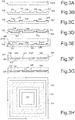
- figure 3A shows an auxiliary wafer 330 of semiconductor material, for example of monocrystalline silicon, having a bonding face 330A.
- the auxiliary wafer 330 is etched, starting from its bonding face 330A, by dry or wet silicon etching (for example, by TMAH - tetramethylammonium hydrate - or KOH - potassium hydroxide) for forming a bonding recess 331 and, in the embodiment shown, a functional recess 332, as represented in the top plan view of figure 3G .
- the bonding recess 331 here surrounds the functional recess 332 and has a closed shape, for example rectangular.
- the bonding recess 331 has a depth comprised between 1 ⁇ m and 20 ⁇ m and a width comprised between 10 ⁇ m and 1 mm;
- the functional recess 332 to be overlaid by a MEMS structure (as explained hereinafter) and having the function of enabling movement thereof, has dimensions linked to the overlying MEMS structure.
- the functional recess 332 may have the same depth as the bonding recess or a greater depth (obtained through a suitably designed further etch) or the same depth as the bonding recess 31.
- projecting portions 334 are formed at the sides of the bonding recess 331.
- an etch-stop layer 333 for example of silicon oxide, is deposited on the auxiliary wafer 330 and coats the entire top surface of the auxiliary wafer 330.
- a material forming a bonding mass 335 is deposited on the etch-stop layer 333.
- a bonding layer 338 for example of glass frit, polymeric material (e.g., a dry film of BCB - benzocyclobutene) or of an eutectic material (e.g., formed by alternating layers, such as Al-Ge, Au-Ge, Au-Sn, Cu-Sn) or a thermocompression metal, such as Au-Au or Cu-Cu, is deposited.
- the bonding layer 338 has a total height greater than that of the bonding recess 331, for example from 1-2 ⁇ m for eutectic material, to approximately 20 ⁇ m for glass frit, up to 50 ⁇ m, for dry film and 1-20 ⁇ m for thermocompression metal.
- the bonding layer 338 is then defined , figure 3D , to be removed on the outside of the bonding recess 331 and to have a width smaller than that of the bonding recess 331, for the reasons explained hereinafter (see also the dashed line in figure 3H . In this way, the bonding mass 335 has a greater height than the projecting portions 334 and projects from the bonding recess 331.
- the auxiliary wafer 330 is then fixed to a device wafer 340, of semiconductor material, for example monocrystalline silicon, having a bonding face 340A, figure 3E .
- the bonding face 340A of the device wafer 340 is brought in abutment with the projecting portions 334 of the auxiliary wafer 330.
- the wafers 330, 340 are then bonded together by applying appropriate pressure and heat, typically according to the materials, in a way known to the person skilled in the art. For instance, bonding is carried out at a temperature of around 280°C in case of eutectic material with an Au-Sn base, of around 420°C in case of a eutectic material with an Au-Ge base, at temperatures lower than 200°C in case of polymeric materials, at approximately 450°C in case of glass frit, and at approximately 400°C in case of thermocompression metal. In the latter case, bonding is carried out at high pressure, for example higher than 20 MPa. Consequently, the bonding mass 335 is compressed and may possibly expand laterally to form a bonding structure 336 that has a chemico-physical bond with the auxiliary wafer 330 and the device wafer 340.
- a composite wafer 341 is thus formed having a cavity 342 at the bonding recess 331 of the auxiliary wafer 330, figure 3F .
- the cavity 342 thus has a closed shape, for example rectangular, and accommodates the bonding structure 336, which is sealed from the adjacent projecting portions 334, in abutment with the bonding surface 340A of the device wafer 340.
- the bonding structure 336 does not contaminate the other areas of the device wafer 340, for example the functional areas where the MEMS structures are to be formed, since it is contained in the cavity 342.
- a chemico-physical bond may be obtained between the etch-stop layer 333 and the device wafer 340, contributing to bonding of the wafers 330 and 340 and further sealing the cavity 342.
- the composite wafer 341 is processed to provide the desired MEMS structures, removing, for example, portions of the device wafer 340 and forming, for example, a suspended platform 345 arranged above the functional recess 332.
- the bonding structure 336 is not exposed to the chemical substances used for defining the MEMS structures and/or for cleaning, since it is sealed inside the cavity 342. Consequently, a wet-etching process may also be used. Even if chemical substances seep into the cavity, the amount of these substances would be very low and would not jeopardize the overall integrity of the bonding structure 336.
- the MEMS structure comprises a platform 445.
- a functional recess 432 having a greater depth than the cavity 442, extends underneath the platform 445 to enable a sufficient mobility of the platform, in particular a sufficient angle of rotation.
- a reflecting layer 460 extends on the platform 445.
- contact pads 461 are formed on the auxiliary wafer 430, extend through the etch-stop layer 433 (operating also as an insulation) and are accessed through openings 463 in the device wafer 440.
- Figure 5 shows a different micromirror device 450, where the device wafer 340 is replaced by a double wafer 540, formed by two silicon layers 571-572 (for example, a monocrystalline-silicon substrate and a polycrystalline-silicon layer grown on top) for forming offset mobile/fixed electrodes on two different levels.
- An insulation layer 573 extends selectively between the two silicon layers.
- the bonding structures 436, 536 are accommodated in cavities 442, 542 enclosed between an auxiliary substrate 430, 530 and a device substrate 440, 540, having a single or double layer, due to the presence of a recess in the auxiliary substrate 430, 530 and to the presence of projecting regions 434, 534 of the auxiliary substrate 430, 530 in contact with the device substrate 440, 540, through an etch-stop layer 433, 533.
- the bonding structures 436, 536 bond the device substrate 440, 540 and the auxiliary substrate 430, 530 and extend along a line surrounding the microelectromechanical structure 445, 545, preferably along a closed line, such as the perimeter of a rectangle.
- Figures 6A and 6B show an embodiment wherein the bonding recesses are formed in a hard-stop layer.
- the manufacturing process comprises depositing and patterning a hard-stop layer to form projecting regions 634 above a first wafer 630, for example the auxiliary wafer.
- the hard-stop layer, and thus the projecting regions 634 are made of a material that is mechanically resistant to pressure (or in any case less compliant than the bonding mass 635), such as polycrystalline silicon, for example deposited epitaxially and patterned via silicon etching.
- a dielectric material may be used, such as PECVD (Plasma-Enhanced Chemical Vapor Deposition) or LPCVD (Low-Pressure Chemical Vapor Deposition) deposited oxide or thermally grown oxide, patterned by dry-etching or wet-etching; a metal, such as Au, Al, deposited by PVD (Physical Vapor Deposition) and patterned by dry or wet etching; or a metal, such as gold, selectively deposited by electrochemical deposition; or a photosensitive polyimide layer.
- PECVD Plasma-Enhanced Chemical Vapor Deposition
- LPCVD Low-Pressure Chemical Vapor Deposition
- the projecting regions 634 delimit at least one bonding recess 631 having a similar shape to the bonding recess 331 of figure 3G .
- a bonding mass 635 is deposited, similarly to what above described for the bonding mass 335 of figures 3C-3G . Also here, the bonding mass 635 has a height greater than the projecting regions 634.
- a second wafer 640 for example the device wafer, is fixed to the first wafer 630, causing it to adhere to the projecting portions 634 of the first wafer 630 and thus compressing the bonding mass 635, which also couples to the second wafer 640, bonding it to the first wafer 630.
- the second wafer 640 thus closes the bonding recess 631 at the top, forming a cavity 642 sealed to the outside.
- figure 7 , the bonding recess 731 and the bonding mass 735 are formed in the device wafer 740.
- the auxiliary wafer 730 has a functional recess 732.
- the auxiliary wafer 830 forms the functional recess 832, whereas the bonding recess 831 is formed in the device wafer 840. Furthermore, here, the bonding regions 836 are formed on the auxiliary wafer 830, in a position such as to be arranged inside the bonding recess 831 during coupling of the wafers 830, 840.
- Figures 9A and 9B show two process steps of an embodiment useful when the bonding material risks contaminating other portions of the device.
- one of the two wafers here the auxiliary wafer 930, has containment trenches 990A, 990B extending from the bonding recess 931 towards the inside of the auxiliary wafer 930.
- two containment trenches 990A, 990B are formed near the external and internal perimeter, respectively, of the bonding recess 931, so as to extend on the sides of the bonding mass 935 prior to bonding the wafers 930, 940 , figure 9A ).
- the bonding mass 935 melted by the high temperature and compressed when the two wafers 930, 940 are brought near and into abutment to each other, may flow inside the containment trenches 990A, 990B, as represented in figure 9B .
- the containment trenches 990A, 990B may prevent overflow of the material from of the cavity 942. This is useful in particular when the bonding regions 936 are made of glass frit or eutectic material.
- the bonding regions are arranged inside a closed cavity, within the device. In this way, the bonding regions are protected from chemical materials used in the process steps after bonding the wafers, preventing them from being damaged and, in the case of partial etching, preventing contamination of the "useful" area of the device.
- the bonding regions are protected from the external environment also during operation of the device, which thus may have a longer service life.
- micromachined devices of a different type comprising bonding of two wafers, as in the case of bulk micromachining of microelectromechanical devices, such as pressure sensors.
- all the embodiments represented may have an etch-stop layer, similar to layer 333 of figures 3C-3F .
- the embodiment of figures 3A-3G may be without the etch-stop layer, if the etching processes so allow.
- the etch-stop layer may extend also on the sensor wafer and/or only in the silicon etching areas.
- containment trenches similar to the trenches 990A, 990B of figures 9A and 9B may be provided also in the embodiments of figures 4-8 .
- the bonding structure may have a non-continuous shape, and may comprise two or more portions arranged along and inside the bonding recess, provided that they define as a whole a sufficient bonding area.
- the bonding recess may have a non-continuous shape, and comprise two or more portions arranged in succession along a closed line or a spiral.
- the bonding structure may comprise a number of bonding portions, with one or more bonding portions arranged in the recess portions, provided that also in this case as a whole a sufficient bonding area is obtained.
- the bonding structure may be obtained by depositing non-continuous bonding material in the bonding cavity, which, during compression due to bonding, expands also in a longitudinal direction of the cavity (in a direction perpendicular to the plane of the drawing) and forms an approximately continuous bonding structure.
- a microelectromechanical device comprises:
- the first and second substrates are of semiconductor material
- the projecting portions comprise contrast regions of a first material
- the bonding structure is of a second material, for example not a semiconductor, and is more compliant than the first material.
- a process for manufacturing a microelectromechanical device comprises:
Landscapes
- Engineering & Computer Science (AREA)
- Microelectronics & Electronic Packaging (AREA)
- Manufacturing & Machinery (AREA)
- Computer Hardware Design (AREA)
- Micromachines (AREA)
- Pressure Sensors (AREA)
Abstract
A microelectromechanical device having a first substrate (330) of semiconductor material and a second substrate (340) of semiconductor material having a bonding recess (331) delimited by projecting portions (334), monolithic therewith. The bonding recess forms a closed cavity (324) with the first substrate. A bonding structure (336) is arranged within the closed cavity and is bonded to the first and second substrates. A microelectromechanical structure (345) is formed in a substrate chosen between the first and second substrates. The device is manufactured by forming the bonding recess in a first wafer; depositing a bonding mass in the bonding recess, the bonding mass having a greater depth than the bonding recess; and bonding the two wafers.


Description
- The present invention relates to a MEMS device formed by at least two bonded structural layers and to the manufacturing process thereof.
- As is known, micromachining techniques, based upon manufacturing technologies typical of microelectronics, enable obtainment of microsystems, such as microsensors, microactuators, and special micromechanisms, which exploit the excellent mechanical properties of monocrystalline silicon and may be manufactured using the knowledge and advantages typical of microelectronic processes.
- In particular, the bulk-micromachining technique generally comprises bonding the wafer where the MEMS device is to be provided (hereinafter also referred to as device wafer or substrate) to one or more wafers or substrates (for example, handling wafers or substrates, cap wafers or substrates, etc., also referred to hereinafter as auxiliary wafers).
- Typically, the manufacturing process comprises processing the device wafer for defining the desired microelectromechanical structures, for example via dry silicon-etching processes and bonding the device wafer to the auxiliary wafer, for example via adhesive, such as glass frit or polymer, or by a metal bond, for example via a eutectic bond such as Al-Ge, Au-Ge, Au-Sn, Cu-Sn, etc., and subsequent dicing the composite wafer to obtain a plurality of devices.
- The device wafer may even be composite and be obtained by bonding two wafers, for example when a MEMS device has offset comb-fingered driving/sensing electrodes. In this case, two wafers are bonded together, to form the composite wafer, which is bonded to the auxiliary wafer.
- For instance,
figures 1A-1D show typical process steps for manufacturing a MEMS micromirror. - In detail,
figure 1A shows two starting wafers including adevice wafer 1 and anauxiliary wafer 2. Here, an etch-stop layer 3, for example of silicon oxide, extends on the auxiliary wafer, and bondingregions 4, for example of glass frit, polymer or metal, extend over the etch-stop layer 3. - In
figure 1B , the device wafer 1 and theauxiliary wafer 2 are brought into contact and bonded by thebonding regions 4, by exerting a slight pressure and at a preset temperature, to obtain abonded wafer 5. - In
figure 1C , thedevice wafer 1 is processed for defining suspended masses of the desired micromechanical structures. For instance, for forming a micromirror, the micromirror structure, supporting arms, actuation electrodes (for example, of a comb-fingered type), and elastic springs are defined. In particular, definition comprises removing the semiconductor material throughout the thickness of the device wafer, and forming throughtrenches 7. In this step, theauxiliary wafer 2 is not etched, being protected by the etch-stop layer 3 and by a possible peripheral protective layer. - In
figure 1D , a reflectingsurface 8 is formed, by depositing and patterning a metal layer. -
figures 2A-2D show a different manufacturing process, for example for manufacturing an inertial sensor, wherein adevice wafer 11 has an etch-stop layer 13, and anauxiliary wafer 12 has bondingregions 14 ,figure 2A ). Similarly tofigures 1A-1D , the process comprises bringing the wafers 11-12 into contact,figure 2B ), defining micromechanical structures 15 (in particular, a sensing mass, actuation/sensing electrodes (for example, of a comb-fingered type) and elastic springs, by etching the semiconductor material of thedevice wafer 11 ,figure 2C ); and selectively removing the etch-stop layer 13, for example by HF etching. - In a way not shown, the
auxiliary wafer 12 may comprises cavities enabling a sufficient movement of the suspended masses. - With the manufacturing processes described with reference to
figures 1 and2 , it is possible to form MEMS scanning micromirrors, inertial sensors, and other sensors, such as gyroscopes, resonators, and electromagnetically actuated scanning micromirrors. - Furthermore, with these manufacturing processes, the problem exists that the bonding regions may be damaged or even partially removed when defining the structures and/or removing the etch-stop layers. In fact, to carry out wet etching, for example for removing the photoresist layer and for cleaning the polymers from the walls of the operating regions, and for carrying out vapour etching, for example for HF cleaning or releasing structures, chemical substances are used that may damage the bonding regions.
- Consequently the choice of the material of the bonding regions is limited to materials capable of withstanding the above processes.
- This imposes, however, design limitations and does not always enable optimal materials to be used.
- The aim of the present invention is to provide a device and a manufacturing process overcoming the drawbacks of the prior art.
- According to the present invention a micromachined semiconductor device and a corresponding manufacturing process are provided, as defined in the attached claims.
- In practice, the bonding layer between two wafers is accommodated inside a cavity formed on the surface of one of the two wafers. The bonding layer is deposited with a thickness slightly greater than the depth of the cavity and is compressed during bonding. In this way, after bonding the two wafers, the bonding layer is completely housed in a cavity, and the latter is completely surrounded by abutting portions of the wafers, which form a sort of seal for the cavity. Consequently, the bonding layer is protected inside the cavity and is not exposed to chemical substances in the subsequent steps.
- For a better understanding of the present invention, preferred embodiments thereof are now described, purely by way of non-limiting example, with reference to the attached drawings, wherein:
-
figures 1A-1D are cross-sections of semiconductor material wafers in successive steps of a known manufacturing process; -
figures 2A-2D are cross-sections of semiconductor material wafers in successive steps of another known manufacturing process; -
figures 3A-3G are cross-sections of semiconductor material wafers in successive steps of an embodiment of the present manufacturing process; -
figure 3H is a top plan view of a part of the structure offigure 3B ; -
figure 4 is a cross-section of a MEMS device obtained with the process offigures 3A-3H ; -
figure 5 is a cross-section of another MEMS device obtained with the process offigures 3A-3H ; -
figures 6A-6B are cross-sections of semiconductor material wafers in successive steps of a different embodiment of the present manufacturing process; -
figures 7 and 8 are cross-sections of different embodiments of the present process; and -
figures 9A-9B are cross-sections of semiconductor material wafers in successive steps of yet another embodiment of the present manufacturing process. - In the attached figures, similar elements are designated in the various figures starting from the numbering used for the embodiment of
figures 3A-3G , adding each time 100, so that, in each figure, the first digit (the hundreds) indicates the number of that figure, and the other two digits (the tens and the units) designate elements that are similar in all the figures. -
figure 3A shows anauxiliary wafer 330 of semiconductor material, for example of monocrystalline silicon, having abonding face 330A. - In
figure 3B , theauxiliary wafer 330 is etched, starting from itsbonding face 330A, by dry or wet silicon etching (for example, by TMAH - tetramethylammonium hydrate - or KOH - potassium hydroxide) for forming abonding recess 331 and, in the embodiment shown, afunctional recess 332, as represented in the top plan view offigure 3G . Thebonding recess 331 here surrounds thefunctional recess 332 and has a closed shape, for example rectangular. For instance, thebonding recess 331 has a depth comprised between 1 µm and 20 µm and a width comprised between 10 µm and 1 mm; thefunctional recess 332, to be overlaid by a MEMS structure (as explained hereinafter) and having the function of enabling movement thereof, has dimensions linked to the overlying MEMS structure. In particular, thefunctional recess 332 may have the same depth as the bonding recess or a greater depth (obtained through a suitably designed further etch) or the same depth as the bonding recess 31. In this step, projectingportions 334 are formed at the sides of thebonding recess 331. - Next,
figure 3C , an etch-stop layer 333, for example of silicon oxide, is deposited on theauxiliary wafer 330 and coats the entire top surface of theauxiliary wafer 330. - Then,
figures 3D, 3E , within thebonding recess 331, a material forming abonding mass 335 is deposited on the etch-stop layer 333. To this end,figure 3D , abonding layer 338, for example of glass frit, polymeric material (e.g., a dry film of BCB - benzocyclobutene) or of an eutectic material (e.g., formed by alternating layers, such as Al-Ge, Au-Ge, Au-Sn, Cu-Sn) or a thermocompression metal, such as Au-Au or Cu-Cu, is deposited. Thebonding layer 338 has a total height greater than that of thebonding recess 331, for example from 1-2 µm for eutectic material, to approximately 20 µm for glass frit, up to 50 µm, for dry film and 1-20 µm for thermocompression metal. Thebonding layer 338 is then defined ,figure 3D , to be removed on the outside of thebonding recess 331 and to have a width smaller than that of thebonding recess 331, for the reasons explained hereinafter (see also the dashed line infigure 3H . In this way, thebonding mass 335 has a greater height than the projectingportions 334 and projects from thebonding recess 331. - The
auxiliary wafer 330 is then fixed to adevice wafer 340, of semiconductor material, for example monocrystalline silicon, having abonding face 340A,figure 3E . In particular, thebonding face 340A of thedevice wafer 340 is brought in abutment with the projectingportions 334 of theauxiliary wafer 330. - The
wafers bonding mass 335 is compressed and may possibly expand laterally to form abonding structure 336 that has a chemico-physical bond with theauxiliary wafer 330 and thedevice wafer 340. - A
composite wafer 341 is thus formed having acavity 342 at thebonding recess 331 of theauxiliary wafer 330,figure 3F . Thecavity 342 thus has a closed shape, for example rectangular, and accommodates thebonding structure 336, which is sealed from the adjacent projectingportions 334, in abutment with thebonding surface 340A of thedevice wafer 340. Furthermore, thebonding structure 336 does not contaminate the other areas of thedevice wafer 340, for example the functional areas where the MEMS structures are to be formed, since it is contained in thecavity 342. - In this step, also a chemico-physical bond may be obtained between the etch-
stop layer 333 and thedevice wafer 340, contributing to bonding of thewafers cavity 342. - Next,
figure 3G , thecomposite wafer 341 is processed to provide the desired MEMS structures, removing, for example, portions of thedevice wafer 340 and forming, for example, a suspendedplatform 345 arranged above thefunctional recess 332. In this step, thebonding structure 336 is not exposed to the chemical substances used for defining the MEMS structures and/or for cleaning, since it is sealed inside thecavity 342. Consequently, a wet-etching process may also be used. Even if chemical substances seep into the cavity, the amount of these substances would be very low and would not jeopardize the overall integrity of thebonding structure 336. - In this way, it is possible, for example, to form a
micromirror device 450, as represented infigure 4 . In this figure, the MEMS structure comprises aplatform 445. Here, afunctional recess 432, having a greater depth than thecavity 442, extends underneath theplatform 445 to enable a sufficient mobility of the platform, in particular a sufficient angle of rotation. A reflectinglayer 460 extends on theplatform 445. Furthermore,contact pads 461 are formed on theauxiliary wafer 430, extend through the etch-stop layer 433 (operating also as an insulation) and are accessed through openings 463 in thedevice wafer 440. -
Figure 5 shows adifferent micromirror device 450, where thedevice wafer 340 is replaced by adouble wafer 540, formed by two silicon layers 571-572 (for example, a monocrystalline-silicon substrate and a polycrystalline-silicon layer grown on top) for forming offset mobile/fixed electrodes on two different levels. Aninsulation layer 573 extends selectively between the two silicon layers. - In both cases, the
bonding structures cavities auxiliary substrate device substrate auxiliary substrate regions auxiliary substrate device substrate stop layer - The
bonding structures device substrate auxiliary substrate microelectromechanical structure -
Figures 6A and 6B show an embodiment wherein the bonding recesses are formed in a hard-stop layer. - Here,
figure 6A , the manufacturing process comprises depositing and patterning a hard-stop layer to form projectingregions 634 above afirst wafer 630, for example the auxiliary wafer. The hard-stop layer, and thus the projectingregions 634, are made of a material that is mechanically resistant to pressure (or in any case less compliant than the bonding mass 635), such as polycrystalline silicon, for example deposited epitaxially and patterned via silicon etching. Alternatively, a dielectric material may be used, such as PECVD (Plasma-Enhanced Chemical Vapor Deposition) or LPCVD (Low-Pressure Chemical Vapor Deposition) deposited oxide or thermally grown oxide, patterned by dry-etching or wet-etching; a metal, such as Au, Al, deposited by PVD (Physical Vapor Deposition) and patterned by dry or wet etching; or a metal, such as gold, selectively deposited by electrochemical deposition; or a photosensitive polyimide layer. - The projecting
regions 634 delimit at least onebonding recess 631 having a similar shape to thebonding recess 331 offigure 3G . In thebonding recess 631, abonding mass 635 is deposited, similarly to what above described for thebonding mass 335 offigures 3C-3G . Also here, thebonding mass 635 has a height greater than the projectingregions 634. - Next,
figure 6B , asecond wafer 640, for example the device wafer, is fixed to thefirst wafer 630, causing it to adhere to the projectingportions 634 of thefirst wafer 630 and thus compressing thebonding mass 635, which also couples to thesecond wafer 640, bonding it to thefirst wafer 630. Thesecond wafer 640 thus closes thebonding recess 631 at the top, forming acavity 642 sealed to the outside. - In yet another embodiment,
figure 7 , thebonding recess 731 and thebonding mass 735 are formed in thedevice wafer 740. Theauxiliary wafer 730 has afunctional recess 732. - In
figure 8 , theauxiliary wafer 830 forms thefunctional recess 832, whereas thebonding recess 831 is formed in thedevice wafer 840. Furthermore, here, the bonding regions 836 are formed on theauxiliary wafer 830, in a position such as to be arranged inside thebonding recess 831 during coupling of thewafers -
Figures 9A and 9B show two process steps of an embodiment useful when the bonding material risks contaminating other portions of the device. To prevent this, one of the two wafers, here theauxiliary wafer 930, hascontainment trenches bonding recess 931 towards the inside of theauxiliary wafer 930. For instance, here, twocontainment trenches bonding recess 931, so as to extend on the sides of thebonding mass 935 prior to bonding thewafers figure 9A ). - During coupling of the
wafers bonding mass 935, melted by the high temperature and compressed when the twowafers containment trenches figure 9B . In this way, thecontainment trenches cavity 942. This is useful in particular when thebonding regions 936 are made of glass frit or eutectic material. - With the solution described, as explained above, the bonding regions are arranged inside a closed cavity, within the device. In this way, the bonding regions are protected from chemical materials used in the process steps after bonding the wafers, preventing them from being damaged and, in the case of partial etching, preventing contamination of the "useful" area of the device.
- Furthermore, the bonding regions are protected from the external environment also during operation of the device, which thus may have a longer service life.
- The described solution may be applied to micromachined devices of a different type comprising bonding of two wafers, as in the case of bulk micromachining of microelectromechanical devices, such as pressure sensors.
- Finally, it is clear that modifications and variations may be made to the device and the manufacturing process described and illustrated herein, without thereby departing from the scope of the present invention, as defined in the attached claims.
- For instance, the various described embodiments may be combined for providing further solutions.
- In particular, all the embodiments represented may have an etch-stop layer, similar to
layer 333 offigures 3C-3F . Alternatively, also the embodiment offigures 3A-3G may be without the etch-stop layer, if the etching processes so allow. Where present, the etch-stop layer may extend also on the sensor wafer and/or only in the silicon etching areas. Furthermore, containment trenches similar to thetrenches figures 9A and 9B may be provided also in the embodiments offigures 4-8 . - The bonding structure may have a non-continuous shape, and may comprise two or more portions arranged along and inside the bonding recess, provided that they define as a whole a sufficient bonding area.
- Also the bonding recess, and the corresponding cavity, may have a non-continuous shape, and comprise two or more portions arranged in succession along a closed line or a spiral. In this case, also the bonding structure may comprise a number of bonding portions, with one or more bonding portions arranged in the recess portions, provided that also in this case as a whole a sufficient bonding area is obtained.
- As an alternative or in addition to the containment trenches, the bonding structure may be obtained by depositing non-continuous bonding material in the bonding cavity, which, during compression due to bonding, expands also in a longitudinal direction of the cavity (in a direction perpendicular to the plane of the drawing) and forms an approximately continuous bonding structure.
- According to one aspect of the present description, a microelectromechanical device comprises:
- a first substrate;
- a second substrate;
- a microelectromechanical structure formed in the first substrate;
- projecting portions formed between the first and second substrates;
- a closed cavity, delimited between the projecting portions, the first and second substrates; and
- a bonding structure inside the closed cavity, the bonding structure bonding the first and second substrates to each other.
- According to another aspect of the present invention, the first and second substrates are of semiconductor material, the projecting portions comprise contrast regions of a first material, and the bonding structure is of a second material, for example not a semiconductor, and is more compliant than the first material.
- According to yet another aspect of the present invention, a process for manufacturing a microelectromechanical device comprises:
- forming a microelectromechanical structure in a first substrate or in a second substrate;
- in the first substrate, forming projecting portions delimiting a bonding recess;
- depositing bonding material on the first substrate or on a second substrate, at the bonding recess; and
- bringing the second substrate into contact with the projecting portions, the bonding recess forming a closed cavity delimited between the projecting portions and the first and second substrates; and
- bonding the first and second substrates, causing the bonding material to bond to the first and second wafers and forming a bonding structure inside the closed cavity.
Claims (15)
- A microelectromechanical device comprising:a first substrate (330; 430; 530; 740; 840; 930) of semiconductor material, having a first face (330A);a second substrate (340; 440; 540; 730; 830; 940) of semiconductor material, having a second face (430A) looking toward the first face of the first substrate, the second substrate having a bonding recess (331; 731; 831; 931) delimited by projecting portions (334; 734; 834; 934) of the second substrate, monolithic therewith, the bonding recess forming a closed cavity (324; 442; 542; 742; 842; 942) with the first face of the first substrate;a bonding structure (336; 436; 536; 736; 836; 936) inside the closed cavity, the bonding structure being bonded to the first and second substrates; anda microelectromechanical structure (35; 445; 545) formed in a substrate chosen between the first and second substrates.
- A device according to claim 1, wherein the closed cavity (324; 442; 542; 742; 842; 942) is arranged along a line surrounding the microelectromechanical structure (35; 445; 545), the line preferably being a closed line.
- A device according to claim 1 or 2, further comprising a functional recess (332; 432; 532; 732; 832; 932) extending in the first substrate (330; 430; 530; 740; 840; 930) or in the second substrate (340; 440; 540; 730; 830; 940) starting from the first face (330A) or from the second face (340A), respectively, in front of the microelectromechanical structure (35; 445; 545).
- A device according to any of the preceding claims, wherein the bonding structure (336; 436; 536; 736; 836; 936) is of a material chosen from glass frit, polymer, eutectic metal, and thermocompression metal.
- A device according to any of the preceding claims, comprising an etch-stop layer (333; 433; 533) extending on the first face (330A) or on the second face (340A).
- A device according to any of the preceding claims, further comprising at least one containment trench (990) extending in the first substrate or in the second substrate (930) at the cavity (942).
- A device according to any of the preceding claims, forming a device chosen from a micromirror, an inertial sensor, and a pressure sensor.
- A process for manufacturing a microelectromechanical device comprising:forming a microelectromechanical structure in a first or in a second substrate of semiconductor material, the first substrate having a first face, and the second substrate having a second face;forming, in the second substrate, starting from the second face, a bonding recess delimited by projecting portions monolithic with the second substrate;depositing, on the first or on the second substrate, a bonding mass in an area corresponding to the bonding recess; andbonding the first and second substrates through the bonding material, bringing the projecting portions of the second substrate into contact with the first surface of the first substrate and forming a closed cavity, delimited between the projecting portions and the first and second substrates and surrounding the bonding mass.
- A process according to claim 8, wherein the bonding mass, prior to the bonding, has a greater height than a depth of the bonding recess, and the bonding step comprises compressing the bonding mass to form a bonding structure.
- A process according to claim 8 or 9, wherein the bonding mass is of a material chosen from glass frit, polymer, eutectic metal, and thermocompression metal.
- A process according to any of claims 8-10, wherein the bonding step is carried out at a temperature comprised between 150°C and 450°C.
- A process according to any of claims 8-11, wherein the cavity is arranged along a line surrounding the microelectromechanical structure on the outside.
- A process according to any of claims 8-12, further comprising forming an etch-stop layer on the first or on the second face.
- A process according to any of claims 8-13, further comprising forming, in the first or in the second substrate, a functional recess extending from the first face or from the second face, respectively, in front of the microelectromechanical structure.
- A process according to any of claims 8-14, further comprising forming at least one containment trench in the first or in the second substrate in an area corresponding to the cavity, and the bonding step comprises compressing the bonding mass and causing the bonding mass to flow into the containment trench.
Applications Claiming Priority (1)
| Application Number | Priority Date | Filing Date | Title |
|---|---|---|---|
| ITUA2016A004673A ITUA20164673A1 (en) | 2016-06-27 | 2016-06-27 | MEMS DEVICE FORMED BY AT LEAST TWO MULTI-PURPOSED STRUCTURAL LAYERS AND RELATIVE PROCESS OF MANUFACTURE |
Publications (1)
| Publication Number | Publication Date |
|---|---|
| EP3263517A1 true EP3263517A1 (en) | 2018-01-03 |
Family
ID=57184729
Family Applications (1)
| Application Number | Title | Priority Date | Filing Date |
|---|---|---|---|
| EP16206887.8A Withdrawn EP3263517A1 (en) | 2016-06-27 | 2016-12-23 | Mems device formed by at least two bonded structural layers and manufacturing process thereof |
Country Status (4)
| Country | Link |
|---|---|
| US (3) | US10227233B2 (en) |
| EP (1) | EP3263517A1 (en) |
| CN (2) | CN206635022U (en) |
| IT (1) | ITUA20164673A1 (en) |
Cited By (1)
| Publication number | Priority date | Publication date | Assignee | Title |
|---|---|---|---|---|
| US12002812B2 (en) | 2021-03-08 | 2024-06-04 | Infineon Technologies Dresden GmbH & Co. KG | Method of producing a semiconductor component and semiconductor component |
Families Citing this family (12)
| Publication number | Priority date | Publication date | Assignee | Title |
|---|---|---|---|---|
| US11078075B2 (en) | 2015-12-31 | 2021-08-03 | Taiwan Semiconductor Manufacturing Company Ltd. | Packaging method and associated packaging structure |
| ITUA20164673A1 (en) * | 2016-06-27 | 2017-12-27 | St Microelectronics Srl | MEMS DEVICE FORMED BY AT LEAST TWO MULTI-PURPOSED STRUCTURAL LAYERS AND RELATIVE PROCESS OF MANUFACTURE |
| US10800649B2 (en) | 2016-11-28 | 2020-10-13 | Analog Devices International Unlimited Company | Planar processing of suspended microelectromechanical systems (MEMS) devices |
| US10266389B2 (en) * | 2017-07-31 | 2019-04-23 | Infineon Technologies Dresden Gmbh | Forming an offset in an interdigitated capacitor of a microelectromechanical systems (MEMS) device |
| CN108324201B (en) * | 2018-05-08 | 2023-11-17 | 杨勇 | Mop with a handle |
| CN108609574B (en) * | 2018-05-31 | 2019-12-31 | 中国科学院微电子研究所 | Enclosed structure, its manufacturing method and device |
| IT201900000917A1 (en) * | 2019-01-22 | 2020-07-22 | St Microelectronics Srl | MANUFACTURING METHOD OF AN INTEGRATED COMPONENT WITH IMPROVED SPACE EMPLOYMENT, AND INTEGRATED COMPONENT |
| US10843920B2 (en) * | 2019-03-08 | 2020-11-24 | Analog Devices International Unlimited Company | Suspended microelectromechanical system (MEMS) devices |
| IT202000003862A1 (en) | 2020-02-25 | 2021-08-25 | St Microelectronics Srl | SEMICONDUCTOR DEVICE FOR ENVIRONMENTAL DETECTION INCLUDING A CAVITY THAT CAN BE COUPLED TO THE EXTERNAL WORLD AND A MECHANICAL FILTRATION STRUCTURE AND CORRESPONDING MANUFACTURING PROCESS |
| CN112897454B (en) * | 2021-01-20 | 2024-02-23 | 杭州士兰集成电路有限公司 | MEMS device and method of manufacturing the same |
| CN114459666B (en) * | 2022-02-14 | 2023-03-17 | 北京航空航天大学 | A capacitive differential pressure sensor, manufacturing method and application thereof |
| CN119461235B (en) * | 2025-01-15 | 2025-03-21 | 苏州芯镁信电子科技有限公司 | A bonding structure and forming method for MEMS micromirror |
Citations (3)
| Publication number | Priority date | Publication date | Assignee | Title |
|---|---|---|---|---|
| EP2259018A1 (en) * | 2009-05-29 | 2010-12-08 | Infineon Technologies AG | Gap control for die or layer bonding using intermediate layers |
| US20120217638A1 (en) * | 2009-09-01 | 2012-08-30 | Tohoku University | Wiring connection method and functional device |
| DE112012005288T5 (en) * | 2011-12-15 | 2014-09-04 | Omron Corporation | Structure of a binding site and its bonding method as well as electrical component |
Family Cites Families (7)
| Publication number | Priority date | Publication date | Assignee | Title |
|---|---|---|---|---|
| US7121402B2 (en) * | 2003-04-09 | 2006-10-17 | Reactive Nano Technologies, Inc | Container hermetically sealed with crushable material and reactive multilayer material |
| ITTO20010086A1 (en) | 2001-01-30 | 2002-07-30 | St Microelectronics Srl | PROCEDURE FOR SEALING AND CONNECTING PARTS OF ELECTROMECHANICAL, FLUID, OPTICAL MICROSYSTEMS AND DEVICE SO OBTAINED. |
| DE102007044806A1 (en) * | 2007-09-20 | 2009-04-02 | Robert Bosch Gmbh | Micromechanical component and method for producing a micromechanical component |
| EP2269946B1 (en) * | 2009-06-29 | 2018-10-03 | STMicroelectronics Srl | Capped integrated device with protective cap, composite wafer incorporating integrated devices and process for bonding integrated devices with respective protective caps |
| DE102010029709B4 (en) * | 2010-06-04 | 2020-08-06 | Robert Bosch Gmbh | Micromechanical component and method for producing a micromechanical component |
| US9617150B2 (en) * | 2013-10-09 | 2017-04-11 | Taiwan Semiconductor Manufacturing Co., Ltd. | Micro-electro mechanical system (MEMS) device having a blocking layer formed between closed chamber and a dielectric layer of a CMOS substrate |
| ITUA20164673A1 (en) * | 2016-06-27 | 2017-12-27 | St Microelectronics Srl | MEMS DEVICE FORMED BY AT LEAST TWO MULTI-PURPOSED STRUCTURAL LAYERS AND RELATIVE PROCESS OF MANUFACTURE |
-
2016
- 2016-06-27 IT ITUA2016A004673A patent/ITUA20164673A1/en unknown
- 2016-12-14 US US15/379,091 patent/US10227233B2/en active Active
- 2016-12-23 EP EP16206887.8A patent/EP3263517A1/en not_active Withdrawn
- 2016-12-30 CN CN201621483563.1U patent/CN206635022U/en active Active
- 2016-12-30 CN CN201611259550.0A patent/CN107539941B/en active Active
-
2019
- 2019-02-22 US US16/283,254 patent/US10570009B2/en active Active
- 2019-12-09 US US16/708,271 patent/US10954121B2/en active Active
Patent Citations (3)
| Publication number | Priority date | Publication date | Assignee | Title |
|---|---|---|---|---|
| EP2259018A1 (en) * | 2009-05-29 | 2010-12-08 | Infineon Technologies AG | Gap control for die or layer bonding using intermediate layers |
| US20120217638A1 (en) * | 2009-09-01 | 2012-08-30 | Tohoku University | Wiring connection method and functional device |
| DE112012005288T5 (en) * | 2011-12-15 | 2014-09-04 | Omron Corporation | Structure of a binding site and its bonding method as well as electrical component |
Cited By (2)
| Publication number | Priority date | Publication date | Assignee | Title |
|---|---|---|---|---|
| US12002812B2 (en) | 2021-03-08 | 2024-06-04 | Infineon Technologies Dresden GmbH & Co. KG | Method of producing a semiconductor component and semiconductor component |
| US12477823B2 (en) | 2021-03-08 | 2025-11-18 | Infineon Technologies Dresden GmbH & Co. KG | Semiconductor component including an electronic component based on polycrystalline silicon |
Also Published As
| Publication number | Publication date |
|---|---|
| CN107539941A (en) | 2018-01-05 |
| CN206635022U (en) | 2017-11-14 |
| ITUA20164673A1 (en) | 2017-12-27 |
| US20170369309A1 (en) | 2017-12-28 |
| US10227233B2 (en) | 2019-03-12 |
| US10954121B2 (en) | 2021-03-23 |
| US20190185318A1 (en) | 2019-06-20 |
| CN107539941B (en) | 2019-08-13 |
| US10570009B2 (en) | 2020-02-25 |
| US20200123004A1 (en) | 2020-04-23 |
Similar Documents
| Publication | Publication Date | Title |
|---|---|---|
| US10954121B2 (en) | MEMS device formed by at least two bonded structural layers and manufacturing process thereof | |
| US7952189B2 (en) | Hermetic packaging and method of manufacture and use therefore | |
| EP2860532B1 (en) | Mems sensor device with multi-stimulus sensing and method of fabrication | |
| US9035451B2 (en) | Wafer level sealing methods with different vacuum levels for MEMS sensors | |
| KR100833508B1 (en) | MEMs package and its method | |
| US9174836B2 (en) | Integrated bondline spacers for wafer level packaged circuit devices | |
| EP2460763A2 (en) | Wafer level packaging process for MEMS devices | |
| JP2003294451A (en) | Micro inertia sensor and manufacturing method thereof | |
| EP1908727A1 (en) | Wafer-level MEMS package and manufacturing method thereof | |
| JP4708366B2 (en) | Wafer packaging and singulation method | |
| US8704317B2 (en) | Microstructure device with an improved anchor | |
| CN103771332A (en) | Electronic device and manufacturing method thereof | |
| US20080145976A1 (en) | Packaging of Micro Devices | |
| US11267697B2 (en) | Use of an uncoupling structure for assembling a component having a casing | |
| EP2402284A1 (en) | MEMS manufacturing method | |
| CN107032292A (en) | packaging method and related packaging structure | |
| Monajemi et al. | A low cost wafer-level MEMS packaging technology | |
| US9637372B2 (en) | Bonded wafer structure having cavities with low pressure and method for forming | |
| US20050079684A1 (en) | Method of manufacturing an accelerometer | |
| US9505612B2 (en) | Method for thin film encapsulation (TFE) of a microelectromechanical system (MEMS) device and the MEMS device encapsulated thereof | |
| US7531424B1 (en) | Vacuum wafer-level packaging for SOI-MEMS devices | |
| EP3009793A1 (en) | Method of fabricating piezoelectric mems device | |
| CN118929559A (en) | MEMS device and manufacturing process with reduced Z-axis static friction | |
| CN106687407A (en) | Microelectronic package and method of manufacturing a microelectronic package | |
| Jin et al. | A 3-D wafer level hermetical packaging for MEMS |
Legal Events
| Date | Code | Title | Description |
|---|---|---|---|
| PUAI | Public reference made under article 153(3) epc to a published international application that has entered the european phase |
Free format text: ORIGINAL CODE: 0009012 |
|
| AK | Designated contracting states |
Kind code of ref document: A1 Designated state(s): AL AT BE BG CH CY CZ DE DK EE ES FI FR GB GR HR HU IE IS IT LI LT LU LV MC MK MT NL NO PL PT RO RS SE SI SK SM TR |
|
| AX | Request for extension of the european patent |
Extension state: BA ME |
|
| STAA | Information on the status of an ep patent application or granted ep patent |
Free format text: STATUS: THE APPLICATION IS DEEMED TO BE WITHDRAWN |
|
| 18D | Application deemed to be withdrawn |
Effective date: 20180704 |