EP3263516A1 - Micro-electro-mechanical device having a tiltable structure, with detection of the position of the tiltable structure - Google Patents
Micro-electro-mechanical device having a tiltable structure, with detection of the position of the tiltable structure Download PDFInfo
- Publication number
- EP3263516A1 EP3263516A1 EP16206894.4A EP16206894A EP3263516A1 EP 3263516 A1 EP3263516 A1 EP 3263516A1 EP 16206894 A EP16206894 A EP 16206894A EP 3263516 A1 EP3263516 A1 EP 3263516A1
- Authority
- EP
- European Patent Office
- Prior art keywords
- platform
- photodetectors
- light
- slit
- photodetector
- Prior art date
- Legal status (The legal status is an assumption and is not a legal conclusion. Google has not performed a legal analysis and makes no representation as to the accuracy of the status listed.)
- Withdrawn
Links
Images




Classifications
-
- G—PHYSICS
- G02—OPTICS
- G02B—OPTICAL ELEMENTS, SYSTEMS OR APPARATUS
- G02B26/00—Optical devices or arrangements for the control of light using movable or deformable optical elements
- G02B26/08—Optical devices or arrangements for the control of light using movable or deformable optical elements for controlling the direction of light
- G02B26/0816—Optical devices or arrangements for the control of light using movable or deformable optical elements for controlling the direction of light by means of one or more reflecting elements
- G02B26/0833—Optical devices or arrangements for the control of light using movable or deformable optical elements for controlling the direction of light by means of one or more reflecting elements the reflecting element being a micromechanical device, e.g. a MEMS mirror, DMD
-
- B—PERFORMING OPERATIONS; TRANSPORTING
- B81—MICROSTRUCTURAL TECHNOLOGY
- B81B—MICROSTRUCTURAL DEVICES OR SYSTEMS, e.g. MICROMECHANICAL DEVICES
- B81B3/00—Devices comprising flexible or deformable elements, e.g. comprising elastic tongues or membranes
- B81B3/0035—Constitution or structural means for controlling the movement of the flexible or deformable elements
- B81B3/004—Angular deflection
- B81B3/0045—Improve properties related to angular swinging, e.g. control resonance frequency
-
- B—PERFORMING OPERATIONS; TRANSPORTING
- B81—MICROSTRUCTURAL TECHNOLOGY
- B81B—MICROSTRUCTURAL DEVICES OR SYSTEMS, e.g. MICROMECHANICAL DEVICES
- B81B7/00—Microstructural systems ; Auxiliary parts of microstructural devices or systems
- B81B7/008—MEMS characterised by an electronic circuit specially adapted for controlling or driving the same
-
- G—PHYSICS
- G02—OPTICS
- G02B—OPTICAL ELEMENTS, SYSTEMS OR APPARATUS
- G02B26/00—Optical devices or arrangements for the control of light using movable or deformable optical elements
- G02B26/08—Optical devices or arrangements for the control of light using movable or deformable optical elements for controlling the direction of light
- G02B26/0816—Optical devices or arrangements for the control of light using movable or deformable optical elements for controlling the direction of light by means of one or more reflecting elements
- G02B26/0833—Optical devices or arrangements for the control of light using movable or deformable optical elements for controlling the direction of light by means of one or more reflecting elements the reflecting element being a micromechanical device, e.g. a MEMS mirror, DMD
- G02B26/0841—Optical devices or arrangements for the control of light using movable or deformable optical elements for controlling the direction of light by means of one or more reflecting elements the reflecting element being a micromechanical device, e.g. a MEMS mirror, DMD the reflecting element being moved or deformed by electrostatic means
-
- G—PHYSICS
- G02—OPTICS
- G02B—OPTICAL ELEMENTS, SYSTEMS OR APPARATUS
- G02B26/00—Optical devices or arrangements for the control of light using movable or deformable optical elements
- G02B26/08—Optical devices or arrangements for the control of light using movable or deformable optical elements for controlling the direction of light
- G02B26/10—Scanning systems
- G02B26/101—Scanning systems with both horizontal and vertical deflecting means, e.g. raster or XY scanners
-
- G—PHYSICS
- G05—CONTROLLING; REGULATING
- G05F—SYSTEMS FOR REGULATING ELECTRIC OR MAGNETIC VARIABLES
- G05F3/00—Non-retroactive systems for regulating electric variables by using an uncontrolled element, or an uncontrolled combination of elements, such element or such combination having self-regulating properties
- G05F3/02—Regulating voltage or current
- G05F3/08—Regulating voltage or current wherein the variable is DC
- G05F3/10—Regulating voltage or current wherein the variable is DC using uncontrolled devices with non-linear characteristics
- G05F3/16—Regulating voltage or current wherein the variable is DC using uncontrolled devices with non-linear characteristics being semiconductor devices
- G05F3/20—Regulating voltage or current wherein the variable is DC using uncontrolled devices with non-linear characteristics being semiconductor devices using diode- transistor combinations
- G05F3/26—Current mirrors
-
- H—ELECTRICITY
- H02—GENERATION; CONVERSION OR DISTRIBUTION OF ELECTRIC POWER
- H02M—APPARATUS FOR CONVERSION BETWEEN AC AND AC, BETWEEN AC AND DC, OR BETWEEN DC AND DC, AND FOR USE WITH MAINS OR SIMILAR POWER SUPPLY SYSTEMS; CONVERSION OF DC OR AC INPUT POWER INTO SURGE OUTPUT POWER; CONTROL OR REGULATION THEREOF
- H02M1/00—Details of apparatus for conversion
- H02M1/12—Arrangements for reducing harmonics from AC input or output
-
- H—ELECTRICITY
- H02—GENERATION; CONVERSION OR DISTRIBUTION OF ELECTRIC POWER
- H02M—APPARATUS FOR CONVERSION BETWEEN AC AND AC, BETWEEN AC AND DC, OR BETWEEN DC AND DC, AND FOR USE WITH MAINS OR SIMILAR POWER SUPPLY SYSTEMS; CONVERSION OF DC OR AC INPUT POWER INTO SURGE OUTPUT POWER; CONTROL OR REGULATION THEREOF
- H02M1/00—Details of apparatus for conversion
- H02M1/14—Arrangements for reducing ripples from DC input or output
- H02M1/15—Arrangements for reducing ripples from DC input or output using active elements
-
- H—ELECTRICITY
- H02—GENERATION; CONVERSION OR DISTRIBUTION OF ELECTRIC POWER
- H02M—APPARATUS FOR CONVERSION BETWEEN AC AND AC, BETWEEN AC AND DC, OR BETWEEN DC AND DC, AND FOR USE WITH MAINS OR SIMILAR POWER SUPPLY SYSTEMS; CONVERSION OF DC OR AC INPUT POWER INTO SURGE OUTPUT POWER; CONTROL OR REGULATION THEREOF
- H02M1/00—Details of apparatus for conversion
- H02M1/42—Circuits or arrangements for compensating for or adjusting power factor in converters or inverters
-
- H—ELECTRICITY
- H02—GENERATION; CONVERSION OR DISTRIBUTION OF ELECTRIC POWER
- H02M—APPARATUS FOR CONVERSION BETWEEN AC AND AC, BETWEEN AC AND DC, OR BETWEEN DC AND DC, AND FOR USE WITH MAINS OR SIMILAR POWER SUPPLY SYSTEMS; CONVERSION OF DC OR AC INPUT POWER INTO SURGE OUTPUT POWER; CONTROL OR REGULATION THEREOF
- H02M3/00—Conversion of DC power input into DC power output
- H02M3/22—Conversion of DC power input into DC power output with intermediate conversion into AC
- H02M3/24—Conversion of DC power input into DC power output with intermediate conversion into AC by static converters
- H02M3/28—Conversion of DC power input into DC power output with intermediate conversion into AC by static converters using discharge tubes with control electrode or semiconductor devices with control electrode to produce the intermediate AC
- H02M3/325—Conversion of DC power input into DC power output with intermediate conversion into AC by static converters using discharge tubes with control electrode or semiconductor devices with control electrode to produce the intermediate AC using devices of a triode or a transistor type requiring continuous application of a control signal
- H02M3/335—Conversion of DC power input into DC power output with intermediate conversion into AC by static converters using discharge tubes with control electrode or semiconductor devices with control electrode to produce the intermediate AC using devices of a triode or a transistor type requiring continuous application of a control signal using semiconductor devices only
- H02M3/33507—Conversion of DC power input into DC power output with intermediate conversion into AC by static converters using discharge tubes with control electrode or semiconductor devices with control electrode to produce the intermediate AC using devices of a triode or a transistor type requiring continuous application of a control signal using semiconductor devices only with automatic control of the output voltage or current, e.g. flyback converters
-
- H—ELECTRICITY
- H04—ELECTRIC COMMUNICATION TECHNIQUE
- H04N—PICTORIAL COMMUNICATION, e.g. TELEVISION
- H04N9/00—Details of colour television systems
- H04N9/12—Picture reproducers
- H04N9/31—Projection devices for colour picture display, e.g. using electronic spatial light modulators [ESLM]
- H04N9/3141—Constructional details thereof
- H04N9/315—Modulator illumination systems
- H04N9/3155—Modulator illumination systems for controlling the light source
-
- H—ELECTRICITY
- H04—ELECTRIC COMMUNICATION TECHNIQUE
- H04N—PICTORIAL COMMUNICATION, e.g. TELEVISION
- H04N9/00—Details of colour television systems
- H04N9/12—Picture reproducers
- H04N9/31—Projection devices for colour picture display, e.g. using electronic spatial light modulators [ESLM]
- H04N9/3141—Constructional details thereof
- H04N9/3173—Constructional details thereof wherein the projection device is specially adapted for enhanced portability
-
- B—PERFORMING OPERATIONS; TRANSPORTING
- B81—MICROSTRUCTURAL TECHNOLOGY
- B81B—MICROSTRUCTURAL DEVICES OR SYSTEMS, e.g. MICROMECHANICAL DEVICES
- B81B2201/00—Specific applications of microelectromechanical systems
- B81B2201/04—Optical MEMS
- B81B2201/042—Micromirrors, not used as optical switches
-
- B—PERFORMING OPERATIONS; TRANSPORTING
- B81—MICROSTRUCTURAL TECHNOLOGY
- B81B—MICROSTRUCTURAL DEVICES OR SYSTEMS, e.g. MICROMECHANICAL DEVICES
- B81B2203/00—Basic microelectromechanical structures
- B81B2203/03—Static structures
- B81B2203/0315—Cavities
-
- B—PERFORMING OPERATIONS; TRANSPORTING
- B81—MICROSTRUCTURAL TECHNOLOGY
- B81B—MICROSTRUCTURAL DEVICES OR SYSTEMS, e.g. MICROMECHANICAL DEVICES
- B81B2203/00—Basic microelectromechanical structures
- B81B2203/05—Type of movement
- B81B2203/056—Rotation in a plane parallel to the substrate
-
- H—ELECTRICITY
- H02—GENERATION; CONVERSION OR DISTRIBUTION OF ELECTRIC POWER
- H02M—APPARATUS FOR CONVERSION BETWEEN AC AND AC, BETWEEN AC AND DC, OR BETWEEN DC AND DC, AND FOR USE WITH MAINS OR SIMILAR POWER SUPPLY SYSTEMS; CONVERSION OF DC OR AC INPUT POWER INTO SURGE OUTPUT POWER; CONTROL OR REGULATION THEREOF
- H02M1/00—Details of apparatus for conversion
- H02M1/0003—Details of control, feedback or regulation circuits
- H02M1/0025—Arrangements for modifying reference values, feedback values or error values in the control loop of a converter
-
- H—ELECTRICITY
- H02—GENERATION; CONVERSION OR DISTRIBUTION OF ELECTRIC POWER
- H02M—APPARATUS FOR CONVERSION BETWEEN AC AND AC, BETWEEN AC AND DC, OR BETWEEN DC AND DC, AND FOR USE WITH MAINS OR SIMILAR POWER SUPPLY SYSTEMS; CONVERSION OF DC OR AC INPUT POWER INTO SURGE OUTPUT POWER; CONTROL OR REGULATION THEREOF
- H02M1/00—Details of apparatus for conversion
- H02M1/0003—Details of control, feedback or regulation circuits
- H02M1/0032—Control circuits allowing low power mode operation, e.g. in standby mode
-
- H—ELECTRICITY
- H02—GENERATION; CONVERSION OR DISTRIBUTION OF ELECTRIC POWER
- H02M—APPARATUS FOR CONVERSION BETWEEN AC AND AC, BETWEEN AC AND DC, OR BETWEEN DC AND DC, AND FOR USE WITH MAINS OR SIMILAR POWER SUPPLY SYSTEMS; CONVERSION OF DC OR AC INPUT POWER INTO SURGE OUTPUT POWER; CONTROL OR REGULATION THEREOF
- H02M1/00—Details of apparatus for conversion
- H02M1/42—Circuits or arrangements for compensating for or adjusting power factor in converters or inverters
- H02M1/4208—Arrangements for improving power factor of AC input
- H02M1/4225—Arrangements for improving power factor of AC input using a non-isolated boost converter
-
- H—ELECTRICITY
- H02—GENERATION; CONVERSION OR DISTRIBUTION OF ELECTRIC POWER
- H02M—APPARATUS FOR CONVERSION BETWEEN AC AND AC, BETWEEN AC AND DC, OR BETWEEN DC AND DC, AND FOR USE WITH MAINS OR SIMILAR POWER SUPPLY SYSTEMS; CONVERSION OF DC OR AC INPUT POWER INTO SURGE OUTPUT POWER; CONTROL OR REGULATION THEREOF
- H02M1/00—Details of apparatus for conversion
- H02M1/42—Circuits or arrangements for compensating for or adjusting power factor in converters or inverters
- H02M1/4208—Arrangements for improving power factor of AC input
- H02M1/4258—Arrangements for improving power factor of AC input using a single converter stage both for correction of AC input power factor and generation of a regulated and galvanically isolated DC output voltage
-
- Y—GENERAL TAGGING OF NEW TECHNOLOGICAL DEVELOPMENTS; GENERAL TAGGING OF CROSS-SECTIONAL TECHNOLOGIES SPANNING OVER SEVERAL SECTIONS OF THE IPC; TECHNICAL SUBJECTS COVERED BY FORMER USPC CROSS-REFERENCE ART COLLECTIONS [XRACs] AND DIGESTS
- Y02—TECHNOLOGIES OR APPLICATIONS FOR MITIGATION OR ADAPTATION AGAINST CLIMATE CHANGE
- Y02B—CLIMATE CHANGE MITIGATION TECHNOLOGIES RELATED TO BUILDINGS, e.g. HOUSING, HOUSE APPLIANCES OR RELATED END-USER APPLICATIONS
- Y02B70/00—Technologies for an efficient end-user side electric power management and consumption
- Y02B70/10—Technologies improving the efficiency by using switched-mode power supplies [SMPS], i.e. efficient power electronics conversion e.g. power factor correction or reduction of losses in power supplies or efficient standby modes
Definitions
- the present invention relates to a micro-electro-mechanical device having a tiltable structure.
- a micromirror obtained through the MEMS (Micro-Electro-Mechanical Systems) technology, without any loss of generality.
- Micro-electro-mechanical devices having a mirror structure using the technology of semiconductor materials.
- micro-electro-mechanical devices are, for example, used in portable apparatuses, such as portable computers, laptops, notebooks (including ultra-thin notebooks), PDAs, tablets, cellphones, smartphones, etc., for optical applications, in particular for directing light beams generated by a light source according to desired modalities.
- the above devices enable stringent requirements to be met as regards space occupation, both as to area and thickness.
- micro-electro-mechanical mirror devices are used in miniaturized projector modules (so-called picoprojectors), which are able to project images at a distance or to generate desired patterns of light.
- picoprojectors miniaturized projector modules
- Micro-electro-mechanical mirror devices generally include a mirror element suspended over a cavity and formed starting from a body of semiconductor material so as to be mobile, typically with movements of tilting or rotation, for directing the incident light beam as desired.
- Figure 1 is a schematic representation of a picoprojector 9 comprising a light source 1, typically a laser source, generating a light beam 2 formed by three monochromatic beams, one for each base colour, which, through an optical system 3 represented only schematically, is deflected by a mirror element 5 towards a screen 6.
- the mirror element 5 is of a two-dimensional type, controlled so as rotate about a vertical axis A and a horizontal axis B. Rotation of the mirror element 5 about the vertical axis A generates a fast horizontal scan, as shown in Figure 2 . Rotation of the mirror element 5 about the horizontal axis B, perpendicular to the vertical axis A, generates a slow vertical scan, typically of a sawtooth type.
- the picoprojector comprises two micromirrors, arranged in sequence along the path of the light beam 2 and each rotatable about an own axis, and precisely one rotatable about the horizontal axis B and the other rotatable about the vertical axis A, for generating the same scanning scheme as in Figure 2 .
- micromirror systems are in 3D gesture-recognition systems. These normally use a picoprojector and an image-acquisition device, such as a photographic camera.
- the light beam here may be in the range of visible light, of invisible light, or at any useful frequency.
- the picoprojector may be similar to the picoprojector 9 of Figure 1 , and the light beam 2 deflected by the micromirror 5 is used for scanning an object in two directions.
- the picoprojector may project small stripes or bands on the object. Any possible projecting or recessed areas of the object (due to the depth thereof) create deformations in the light rays detected by the photographic camera, which may be processed by suitable electronics for detecting the third dimension.
- the picoprojector comprises a mirror element, rotation whereof is generally controlled via an actuation system, currently of an electrostatic, magnetic, or piezoelectric type.
- FIG. 3 shows a mirror element 5 with purely electrostatic actuation.
- a chip 10 comprises a region 11 suspended over a substrate (not visible), having a reflecting surface (not shown) and supported by a suspended frame 13 by a first pair of arms 12 (first torsion springs).
- the first arms 12 extend from opposite sides of the suspended region 11 and form the rotation axis A of the mirror element 5.
- the suspended frame 13 is connected to a fixed peripheral portion 15 of the chip 10 via a second pair of arms 16 (second torsion springs), which enable rotation of the suspended frame 13 and of the suspended region 11 about the horizontal axis B.
- the first and second arms 12, 16 are coupled to respective actuation assemblies 18A, 18B of an electrostatic type.
- Each actuation assembly 18 A, 18B here comprises first electrodes 19 facing respective second electrodes 20.
- the first electrodes 19 are fixed with respect to the respective arms 12, 16 and are comb-fingered with respect to the second electrodes 20 for generating a capacitive coupling. Due to the arrangement of the electrodes 19, 20 of each actuation assembly 18A, 18B, the driving structure is also defined as "comb drive structure”.
- Rotation of the mirror element 5 about the vertical axis A that produces the horizontal scan occurs generally through an angle of ⁇ 12°, and rotation of the mirror element 5 about the horizontal axis B that produces the vertical scan occurs generally through an angle of ⁇ 8°.
- the angular position of the mirror element to be controlled precisely.
- minor deviations of the physical or electrical characteristics of the structures due to the variability in the production lots, to assembly imprecision, or to variable operating conditions, such as temperature or ageing, may lead to even considerable errors in the direction of the light beam emitted by the mirror element.
- solutions of a capacitive type are markedly non-linear with the angle, so that signal processing is in general complex and burdensome for the processing electronics.
- Solutions of a piezoelectric type require, on the other hand, temperature compensation, which adds complexity to the system and in turn introduces a source of error.
- the aim of the present invention is to provide a detection solution that overcomes the drawbacks of the prior art.
- a micro-electro-mechanical device and a method for detecting rotation are provided, as defined in the attached claims.
- micromirror is rotatable only about one axis.
- it may be modified in a simple way for detection of rotations about two axes, as explained hereinafter.
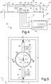
- FIGS 4 and 5 are schematic illustrations of a microelectronic device 50 having a tiltable structure (platform 52), which is able to turn about a rotation axis A.
- the platform 52 is suspended over a cavity 53, formed in a carrying structure 51 and surrounded by a through trench 55.
- the microelectronic device 50 is formed in a first substrate 60 and in a second substrate 61, here bonded to each other by an adhesive layer 63, for example of silicon oxide, glass frit, or other bonding material normally used in MEMS.
- the substrates 60 and 61 may be obtained starting from two wafers of semiconductor material, for example silicon, using known semiconductor manufacture techniques, such as trenching, growing, selective depositing and/or removing, and sawing, in a per known manner.
- the second substrate 61 may be formed from an SOI (Silicon-On-Insulator) substrate, and comprises two semiconductor layers (and precisely a bottom semiconductor layer 57 and a top semiconductor layer 58) separated by an insulating layer 59.
- the bottom semiconductor layer 57 is partially removed to form the cavity 53, and the top semiconductor layer 58 is defined to form the trench 55 surrounding the platform 52.
- the carrying structure 51 is thus formed by the first substrate 60, which delimits the cavity 53 at the bottom, and by walls 54, which delimit the cavity 53 and the through trench 55 laterally and are formed by the second substrate 61.
- the cavity 53 thus has a bottom surface 53A, lying in the same plane as the top surface 60A of the first substrate 60.
- the second substrate 61 has a top surface 61A parallel to the top surface 60A of the first substrate 60.
- the platform 52 has a first side 52a facing the cavity 53 and a top surface (second side 52B) which is the same, in the rest position, with the top surface of the second substrate 61 and carries a reflecting layer 65, for example a metal layer.
- the platform 52 is supported by the carrying structure 51 through a supporting and actuation structure, which is also formed in the top semiconductor layer 58 of the second substrate 61 and comprises (see in particular Figure 5 ) arms 66, torsion springs 67, represented only schematically, and an actuation structure 68, also represented only schematically and formed in any known way, for example of an electrostatic, piezoelectric, or magnetic type.
- the platform 52 and the reflecting layer 65 have a circular shape. They could, however, have any other shape, for example quadrangular, hexagonal, etc., and have their centre of mass B along the rotation axis A.
- the platform 52 and the reflecting layer 65 have a slit 70, preferably arranged in a central position (for example centred on the centre of mass B), extending completely through them.
- the slit 70 has relatively small dimensions so as to intercept a small portion of the light beam impinging upon the reflecting surface 65.
- the slit 70 may have a roughly rectangular shape with major side parallel to the rotation axis A, as visible in particular in Figure 5 . Other shapes or directions are, however, possible.
- the slit 70 may have dimensions comprised between 1 ⁇ m x 10 ⁇ m and 5 ⁇ m x 50 ⁇ m, for example, 3 ⁇ m x 20 ⁇ m.
- the slit 70 has a bottom output edge 70A facing the bottom surface 53A of the cavity 53.
- the second substrate 60 carries an array of photodetectors 71, for example photodiodes, preferably integrated in the semiconductor material of the second substrate 60 and facing the cavity 53.
- the photodetectors 71 may be aligned to each other in a direction perpendicular to the rotation axis A and parallel to the direction of the long side of the slit 70 (direction Y), or arranged in different configurations, as discussed in detail hereinafter with reference to Figures 9-12 .
- the array of photodetectors 71 comprises a central photodetector 71A arranged along the vertical line through the centre of the slit 70 and a plurality of lateral photodetectors 71B arranged at an increasing distance from the central photodetector 71A.
- the photodetectors 71 are connected, through conductive paths 72 represented only schematically, and appropriate interfaces (not shown), to a processing unit 75, which is, for example, arranged in a separate read interface, for instance an ASIC (Application Specific Integrated Circuit).
- the processing unit 75 may be formed in the first substrate 60.
- the processing unit 75 receives the electrical signals generated by the photodetectors 71 and processes them to obtain the rotation angle of the platform 52, as explained hereinafter. To this end, the processing unit 75 comprises a subtractor 76 and a computing unit 77, represented schematically.
- the micro-electro-mechanical device 50 exploits the known phenomenon of diffraction whereby the width of the spot generated on a wall in front of a slit passed by a wave is inversely proportional to the amplitude of the slit, and to very small slits there correspond very wide diffraction fringes.
- FIGS 6A and 6B are schematic illustrations of the microelectronic device 50 in two rotation positions, in the operating hypothesis that the platform 52 is impinged upon by light beam directed perpendicular to the top surface 60A, 60B of the first and second substrates 60, 61.
- the light beam represented schematically and designated by 78, is, for example, generated by a light source, such as the light source 1 of Figure 1 .
- Figure 6A shows the microelectronic device 50 with the platform 52 in the rest position (i.e., not tilted).
- the top surface 52B of the platform 52 and the reflecting layer 65 are arranged parallel to the top surface 53A of the cavity 53 (angle 0°).
- the light beam 78 is perpendicular also to the platform 52 and thus passes through the slit 70 over its entire area (area of the slit 70 visible from above, in Figure 5 ).
- the width of the light beam 80 that reaches the array of photodetectors 71 here has a first width, which is roughly the same as the area of the slit 70, but for diffraction and reflection phenomena, here substantially negligible.
- the small area of the slit 70 is such that only a very small portion of the light beam passes through the slit 70 and is thus "lost" for the operation of the micro-electro-mechanical device 50 as a micromirror (in other words, practically all the light beam 78 is reflected by the reflecting surface 65). In this way, there is no marked reduction of the efficiency of the micro-electro-mechanical device 50.
- the "useful" area of the slit 70 i.e., the projection of the area of the slit 70 in a plane parallel to the top surface 61A of the first substrate 61
- Figure 6B the "useful" area of the slit 70
- a part of the light entering the slit 70 is reflected on the walls of the slit 70 and is scattered in various directions due to the roughness of the walls so that the width of the light beam 81 leaving the slit 70 is further reduced as compared to that of the incoming light beam.
- the width of the light beam 81 decreases at the bottom output edge 70A of the slit 70. It follows that the light beam 81 exiting from the slit 70 widens and, in Figure 6B , reaches an area, on the bottom surface 53A of the cavity 53, much greater than the width for a zero rotation angle of the platform 52 ( Figure 6A ).
- the light intensity I is maximum at the central photodiode 70A (on the graph, normalized to 1) and drops very rapidly as the distance from the central photodetector 71A increases.
- the light intensity I drops practically to zero in the lateral photodetectors 70B arranged at a distance of almost 30 ⁇ m from the central photodiode 70A and then increases slightly again as a result of the side bands due to diffraction.
- the light intensity I detected by the central photodetector 71A decreases to 70% of the maximum value, but the light intensity I detected by the lateral photodetectors 71B decreases more slowly as their distance from the central photodetector 71A increases, as compared to the curve 100.
- a larger number of lateral photodetectors 71B detects a light intensity I of non-zero amplitude.
- the light intensity I detected by the central photodetector 71A is very low (approximately 30% of the maximum value), but the width of the light beam 78 is much greater than for the curves 100 and 120, and the light intensity I detected by the lateral photodetectors 71B decreases very slowly with the distance, so that a still larger number of lateral photodiodes 70B is reached by a light intensity I of a measurable value.
- the value of the light intensity I detected by the photodetectors 71 and its reduction rate in the lateral photodetectors 71B may thus be used as a measure of the rotation angle ⁇ of the platform 52.
- the signals supplied by the photodetectors 71 may provide a direct and unique indication of the rotation angle ⁇ of the platform 52.
- an optimal position of the photodetectors 71 exists where the measured light intensity signal is uniquely linked to the value of the rotation angle ⁇ of the platform 52.
- a position X exists where the difference between the light intensity signal Ic(0, ⁇ ) supplied by the central photodetector 71A, and the light intensity signal I L (x, ⁇ ), supplied by the lateral photodetector 71B arranged at a distance X from the central photodetector 71A, is directly proportional to the rotation angle ⁇ of the platform 52, as discussed hereinafter.
- the array of photodiodes 70 comprises M elements, and the signal of light intensity I generated by them is acquired at K discrete angles ⁇ i .
- M x K values are acquired corresponding to the measured light intensity I.
- the curve of the linearity L 2 shows that there least one point exists (at a distance XM, in the graph approximately 52 ⁇ m) where the curve has the value 1 and thus a linear correlation exists between the light intensity difference DI and the angle ⁇ .
- the test machine controls the microelectronic device 50 so as to measure the light intensity detected by the array of photodetectors 71 for a plurality of angles ⁇ of the platform 52 and calculates the distance XM at which the difference between the light intensity detected by the lateral photodetectors 71B and the light intensity detected by the central photodetector 71A depends directly upon the rotation angle ⁇ .
- the parameters m, q of the specific linear function [2] that links the difference of intensity to the angle ⁇ are obtained.
- the distance XM and the parameters m, q are saved to a suitable memory area of the processing unit 75.
- the processing unit 75 may acquire just the brightness values measured by the central photodetector 71A and by one lateral photodetector 71B arranged at distance XM, compute their difference via the subtractor 76 of Figure 4 and, on the basis of the previously calculated parameters, obtain the instantaneous angle ⁇ . This instantaneous angle value ⁇ may then be processed by the processing unit 75 or supplied to other units for precise feedback control of the angular position of the platform 52.
- the distance XM may be calculated statistically on a production lot, for example on a test device, and this value be used for all the devices of the lot, without searching distance XM for each device.
- the distance XM may be calculated statistically on test structures during the design stage, and the device may comprise an array of photodiodes formed only by the central photodetector 71A and one or more photodetectors 71B arranged stastistically at optimal distance XM or at a short distance therefrom.
- the array of photodiodes may comprise just three photodiodes, arranged as shown in Figure 9 , or the lateral photodetectors 71B may be arranged within an annular area of the top surface 53A of the cavity 53, centred on the central photodetector 71A, as shown schematically in Figure 10 . In this case, according to the dimension of the annular area, during testing it is possible to look for the precise distance XM for each specific device or not.
- the arrangement of the photodetectors 71 may be chosen on the basis of various considerations, such as the fact that the platform 52 is rotatable about one or two axes.
- the photodetectors 71 may be arranged according to a two-dimensional configuration, for example according to a rectangular, square or circular array, as shown schematically in Figures 11 and 12 , or according to any other suitable shape, for example an oval, a polygon, annular sectors, etc.
- a two-dimensional (quadrangular, circular, or annular) configuration may be chosen also when the platform is rotatable about a single axis.
- the processing unit 75 may comprise a logic for calculating the distance XM and, in use, verifying, periodically or upon command, whether the optimal distance XM has been modified due to structural deformations, and using the new distance value XM.
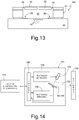
- Figure 13 shows a micro-electro-mechanical device 150 in which the top surface 53A of the cavity 53 has an anti-reflecting structure 90.
- the anti-reflecting structure is formed outside the area of the photodetectors 71, near the periphery of the top surface 53A, underneath the trench 55.
- the anti-reflecting structure 90 may be formed by depositing a stack of different dielectric layers or by forming a roughness of the top surface 53A, for example by silicon etch, in a known manner.
- any possible light filtering within the cavity 53 through the trench 55 is randomly scattered and absorbed in a practically uniform way, without creating any possible reflections focused on specific photodetectors 71, such as to generate spurious signals.
- the micro-electro-mechanical devices 50, 150 may be manufactured by wafer-to-wafer bonding at the front-end level, and subsequent sawing into single devices. Alternatively, they may be manufactured as SoC (System-on-Chip), by assembling a MEMS structure on a chip of photodetectors.
- SoC System-on-Chip
- the slit 70 may be formed by DRIE (Deep Reactive Ion Etching), for example in the same step as, or in a step separate from, definition of the platform 52 and of the actuation structures, or in general of the micro-electro-mechanical structure.
- DRIE Deep Reactive Ion Etching
- the micro-electro-mechanical device 150 may thus be manufactured using micromachining techniques that are standard in the semiconductors industry, with costs that are not high and with a good reliability.
- the micro-electro-mechanical device 50, 150 may be used in a picoprojector 101 designed to be functionally coupled to a portable electronic apparatus 100, as illustrated hereinafter with reference to Figures 14-16 .
- the picoprojector 101 of Figure 14 comprises a light source 102, for example of a laser type, designed to generate a light beam 103; the micro-electro-mechanical device 50, 150, designed to receive the light beam 103 and direct it towards a screen or display surface 105 (external and arranged at a distance from the picoprojector 101); a first driving circuit 106, designed to supply appropriate control signals to the light source 102, for generating the light beam 103 according to an image to be projected; a second driving circuit 108, designed to supply driving signals for rotating the platform 52 ( Figures 4 and 13 ) of the micro-electro-mechanical device 50, 150; and a communication interface 109, designed to receive, from an external control unit 110, for example included in the portable apparatus 100 ( Figures 9, 10 ), light information on the image to be generated, for example in the form of an array of pixels. The light information is inputted for driving the light source 102.
- a first driving circuit 106 designed to supply appropriate control signals to the light source
- control unit 100 may comprise a unit for controlling the angular position of the mirror of the micro-electro-mechanical device 50, 150. To this end, the control unit 100 may receive the signals generated by the photodetectors 71 (not represented in Figure 14 ) through the interface 109 and accordingly control the second driving circuit 108.
- the picoprojector 101 may be formed as separate stand-alone accessory with respect to an associated portable electronic apparatus 100, for example a cellphone or smartphone, as shown in Figure 15 .
- the picoprojector 101 is coupled to the portable electronic apparatus 100 by suitable electrical and mechanical connection elements (not illustrated in detail).
- the picoprojector 101 has an own housing 141, which has at least one portion 141' transparent to the light beam 103 coming from the microelectronic device 50.
- the housing 141 of the picoprojector 1 is releasably coupled to a respective housing 142 of the portable electronic apparatus 100.
- the picoprojector 101 may be integrated within the portable electronic apparatus 100 and be arranged within the housing 142 of the portable electronic apparatus 100.
- the portable electronic apparatus 100 has a respective portion 142' transparent to the light beam 103 coming from the micro-electro-mechanical device 50, 150.
- the picoprojector 101 is, in this case, for example coupled to a PCB (Printed-Circuit Board) inside the housing 142 of the portable electronic apparatus 100.
- PCB Print-Circuit Board
- the slit 70 could be arranged in a non-central position. For example, it could be arranged in another point of the platform 52, arranging the photodetectors 71 accordingly.
- a further slit could be arranged for detecting a further degree of freedom.
- a further slit could be made in the frame 13. In this case, underneath the further slit photodetectors may be arranged with very high sensitivity so that the little light intercepted by the further slit would enable detection of the movement of the micromirror according to a second degree of freedom.
- the antireflecting portion could be arranged on the side wall of the cavity 53.
- the substrate 60 could be made of a different material, for example not a semiconductor material, such as a PCB, carrying a chip integrating the array of photodetectors, thus using an assembly technology.
Landscapes
- Engineering & Computer Science (AREA)
- Physics & Mathematics (AREA)
- General Physics & Mathematics (AREA)
- Power Engineering (AREA)
- Optics & Photonics (AREA)
- Microelectronics & Electronic Packaging (AREA)
- Computer Hardware Design (AREA)
- Multimedia (AREA)
- Signal Processing (AREA)
- Automation & Control Theory (AREA)
- Radar, Positioning & Navigation (AREA)
- Electromagnetism (AREA)
- Nonlinear Science (AREA)
- Mechanical Light Control Or Optical Switches (AREA)
- Micromachines (AREA)
- Length Measuring Devices By Optical Means (AREA)
Abstract
A micro-electro-mechanical device (50), wherein a platform (52) is formed in a top substrate and is configured to turn through a rotation angle (θ). The platform has a slit (70) and faces a cavity (53). A plurality of integrated photodetectors (70) is formed in a bottom substrate so as to detect the light through the slit and generate signals correlated to the light through the slit. The area of the slit varies with the rotation angle of the platform and causes diffraction, more or less marked as a function of the angle. The difference between the signals of two photodetectors arranged at different positions with respect to the slit yields the angle.
Description
- The present invention relates to a micro-electro-mechanical device having a tiltable structure. In particular, hereinafter reference will be made to a micromirror obtained through the MEMS (Micro-Electro-Mechanical Systems) technology, without any loss of generality.
- Micro-electro-mechanical devices are known having a mirror structure using the technology of semiconductor materials.
- These micro-electro-mechanical devices are, for example, used in portable apparatuses, such as portable computers, laptops, notebooks (including ultra-thin notebooks), PDAs, tablets, cellphones, smartphones, etc., for optical applications, in particular for directing light beams generated by a light source according to desired modalities.
- Thanks to the small dimensions, the above devices enable stringent requirements to be met as regards space occupation, both as to area and thickness.
- For example, micro-electro-mechanical mirror devices are used in miniaturized projector modules (so-called picoprojectors), which are able to project images at a distance or to generate desired patterns of light.
- Micro-electro-mechanical mirror devices generally include a mirror element suspended over a cavity and formed starting from a body of semiconductor material so as to be mobile, typically with movements of tilting or rotation, for directing the incident light beam as desired.
- For example,
Figure 1 is a schematic representation of apicoprojector 9 comprising alight source 1, typically a laser source, generating alight beam 2 formed by three monochromatic beams, one for each base colour, which, through anoptical system 3 represented only schematically, is deflected by amirror element 5 towards ascreen 6. In the example shown, themirror element 5 is of a two-dimensional type, controlled so as rotate about a vertical axis A and a horizontal axis B. Rotation of themirror element 5 about the vertical axis A generates a fast horizontal scan, as shown inFigure 2 . Rotation of themirror element 5 about the horizontal axis B, perpendicular to the vertical axis A, generates a slow vertical scan, typically of a sawtooth type. - The obtained scanning scheme is shown in
Figure 2 and designated by 7. - In a variant of the system of
Figure 1 , the picoprojector comprises two micromirrors, arranged in sequence along the path of thelight beam 2 and each rotatable about an own axis, and precisely one rotatable about the horizontal axis B and the other rotatable about the vertical axis A, for generating the same scanning scheme as inFigure 2 . - Another application of micromirror systems is in 3D gesture-recognition systems. These normally use a picoprojector and an image-acquisition device, such as a photographic camera. The light beam here may be in the range of visible light, of invisible light, or at any useful frequency. The picoprojector may be similar to the
picoprojector 9 ofFigure 1 , and thelight beam 2 deflected by themicromirror 5 is used for scanning an object in two directions. For example, the picoprojector may project small stripes or bands on the object. Any possible projecting or recessed areas of the object (due to the depth thereof) create deformations in the light rays detected by the photographic camera, which may be processed by suitable electronics for detecting the third dimension. - In both cases, with the considered technology, the picoprojector comprises a mirror element, rotation whereof is generally controlled via an actuation system, currently of an electrostatic, magnetic, or piezoelectric type.
- For example,
Figure 3 shows amirror element 5 with purely electrostatic actuation. Here, achip 10 comprises aregion 11 suspended over a substrate (not visible), having a reflecting surface (not shown) and supported by a suspendedframe 13 by a first pair of arms 12 (first torsion springs). Thefirst arms 12 extend from opposite sides of the suspendedregion 11 and form the rotation axis A of themirror element 5. The suspendedframe 13 is connected to a fixedperipheral portion 15 of thechip 10 via a second pair of arms 16 (second torsion springs), which enable rotation of the suspendedframe 13 and of the suspendedregion 11 about the horizontal axis B. The first andsecond arms respective actuation assemblies actuation assembly first electrodes 19 facing respectivesecond electrodes 20. - In detail, the
first electrodes 19 are fixed with respect to therespective arms second electrodes 20 for generating a capacitive coupling. Due to the arrangement of theelectrodes actuation assembly - By applying appropriate voltages between the
first electrodes 19 and thesecond electrodes 20, it is possible to generate attraction/repulsion forces between them and thus cause rotation of thefirst electrodes 19 with respect to thesecond electrodes 20 and torsion of thearms region 11 with respect to axes A, B, and thus scanning in a horizontal direction and in a vertical direction, are obtained. - Rotation of the
mirror element 5 about the vertical axis A that produces the horizontal scan occurs generally through an angle of ±12°, and rotation of themirror element 5 about the horizontal axis B that produces the vertical scan occurs generally through an angle of ±8°. - To function properly, it is desirable for the angular position of the mirror element to be controlled precisely. In fact, minor deviations of the physical or electrical characteristics of the structures, due to the variability in the production lots, to assembly imprecision, or to variable operating conditions, such as temperature or ageing, may lead to even considerable errors in the direction of the light beam emitted by the mirror element.
- To this end, systems for detecting the position of the micromirror element are known in the art, based upon capacitive or piezoelectric principles.
- However, known solutions are not completely satisfactory. In particular, solutions of a capacitive type are markedly non-linear with the angle, so that signal processing is in general complex and burdensome for the processing electronics. Solutions of a piezoelectric type require, on the other hand, temperature compensation, which adds complexity to the system and in turn introduces a source of error.
- The aim of the present invention is to provide a detection solution that overcomes the drawbacks of the prior art.
- According to the present invention, a micro-electro-mechanical device and a method for detecting rotation are provided, as defined in the attached claims.
- For a better understanding of the present invention, preferred embodiments thereof are now described, purely by way of non-limiting example, with reference to the attached drawings, wherein:
-
Figure 1 is a schematic representation of a picoprojector; -
Figure 2 shows the projection scheme of an image generated by the picoprojector ofFigure 1 on a screen; -
Figure 3 is a top plan view of a microelectronic micromirror device with electrostatic actuation; -
Figure 4 is a cross-section of a micro-electro-mechanical micromirror device having a system for detecting the angular position of a platform of the device; -
Figure 5 is a top plan view of a part of the micro-electro-mechanical device ofFigure 4 ; -
Figures 6A and 6B show the structure ofFigure 4 in a simplified way and in two different operating positions; -
Figures 7 and 8 are plots of electrical signals of the device ofFigure 4 ; -
Figures 9-12 show different configurations of arrays of photodetector elements of the device ofFigure 4 ; -
Figure 13 is a cross-section of a different embodiment of the present MEMS device; -
Figure 14 is a block diagram of a picoprojector using the present MEMS device; and -
Figures 15 and 16 show coupling variants between the picoprojector ofFigure 10 and a portable electronic apparatus. - In the following description, for simplicity, embodiments will be described where the micromirror is rotatable only about one axis. However, it may be modified in a simple way for detection of rotations about two axes, as explained hereinafter.
-
Figures 4 and 5 are schematic illustrations of amicroelectronic device 50 having a tiltable structure (platform 52), which is able to turn about a rotation axis A. Theplatform 52 is suspended over acavity 53, formed in acarrying structure 51 and surrounded by a throughtrench 55. - The
microelectronic device 50 is formed in afirst substrate 60 and in asecond substrate 61, here bonded to each other by anadhesive layer 63, for example of silicon oxide, glass frit, or other bonding material normally used in MEMS. Thesubstrates second substrate 61 may be formed from an SOI (Silicon-On-Insulator) substrate, and comprises two semiconductor layers (and precisely abottom semiconductor layer 57 and a top semiconductor layer 58) separated by aninsulating layer 59. Thebottom semiconductor layer 57 is partially removed to form thecavity 53, and thetop semiconductor layer 58 is defined to form thetrench 55 surrounding theplatform 52. - The
carrying structure 51 is thus formed by thefirst substrate 60, which delimits thecavity 53 at the bottom, and bywalls 54, which delimit thecavity 53 and the throughtrench 55 laterally and are formed by thesecond substrate 61. Thecavity 53 thus has abottom surface 53A, lying in the same plane as thetop surface 60A of thefirst substrate 60. Further, thesecond substrate 61 has atop surface 61A parallel to thetop surface 60A of thefirst substrate 60. - The
platform 52 has a first side 52a facing thecavity 53 and a top surface (second side 52B) which is the same, in the rest position, with the top surface of thesecond substrate 61 and carries a reflectinglayer 65, for example a metal layer. Theplatform 52 is supported by thecarrying structure 51 through a supporting and actuation structure, which is also formed in thetop semiconductor layer 58 of thesecond substrate 61 and comprises (see in particularFigure 5 )arms 66,torsion springs 67, represented only schematically, and anactuation structure 68, also represented only schematically and formed in any known way, for example of an electrostatic, piezoelectric, or magnetic type. - In the embodiment shown, the
platform 52 and the reflectinglayer 65 have a circular shape. They could, however, have any other shape, for example quadrangular, hexagonal, etc., and have their centre of mass B along the rotation axis A. - The
platform 52 and the reflectinglayer 65 have aslit 70, preferably arranged in a central position (for example centred on the centre of mass B), extending completely through them. Theslit 70 has relatively small dimensions so as to intercept a small portion of the light beam impinging upon the reflectingsurface 65. For example, theslit 70 may have a roughly rectangular shape with major side parallel to the rotation axis A, as visible in particular inFigure 5 . Other shapes or directions are, however, possible. For instance, theslit 70 may have dimensions comprised between 1 µm x 10 µm and 5 µm x 50 µm, for example, 3µm x 20 µm. Theslit 70 has a bottom output edge 70A facing thebottom surface 53A of thecavity 53. - The
second substrate 60 carries an array ofphotodetectors 71, for example photodiodes, preferably integrated in the semiconductor material of thesecond substrate 60 and facing thecavity 53. Thephotodetectors 71 are manufactured in any known way (see, for example: http://citeseerx.ist.psu.edu/viewdoc/download?doi=10.1.1.30.8072&rep=rep1&type=pd f) and are arranged underneath theslit 70, for example so that the centre of the array is vertically aligned with the centre of theslit 70 and the centre of mass B. As shown schematically inFigure 5 , thephotodetectors 71 may be aligned to each other in a direction perpendicular to the rotation axis A and parallel to the direction of the long side of the slit 70 (direction Y), or arranged in different configurations, as discussed in detail hereinafter with reference toFigures 9-12 . - In particular, in
Figures 4 and 5 , the array ofphotodetectors 71 comprises acentral photodetector 71A arranged along the vertical line through the centre of theslit 70 and a plurality oflateral photodetectors 71B arranged at an increasing distance from thecentral photodetector 71A. - The
photodetectors 71 are connected, throughconductive paths 72 represented only schematically, and appropriate interfaces (not shown), to aprocessing unit 75, which is, for example, arranged in a separate read interface, for instance an ASIC (Application Specific Integrated Circuit). Alternatively, theprocessing unit 75 may be formed in thefirst substrate 60. - The
processing unit 75 receives the electrical signals generated by thephotodetectors 71 and processes them to obtain the rotation angle of theplatform 52, as explained hereinafter. To this end, theprocessing unit 75 comprises asubtractor 76 and acomputing unit 77, represented schematically. - The micro-electro-
mechanical device 50 exploits the known phenomenon of diffraction whereby the width of the spot generated on a wall in front of a slit passed by a wave is inversely proportional to the amplitude of the slit, and to very small slits there correspond very wide diffraction fringes. - This phenomenon is represented in a simplified way in
Figures 6A and 6B (where the secondary peaks are ignored), which are schematic illustrations of themicroelectronic device 50 in two rotation positions, in the operating hypothesis that theplatform 52 is impinged upon by light beam directed perpendicular to thetop surface 60A, 60B of the first andsecond substrates light source 1 ofFigure 1 . - In detail,
Figure 6A shows themicroelectronic device 50 with theplatform 52 in the rest position (i.e., not tilted). Thus, the top surface 52B of theplatform 52 and the reflectinglayer 65 are arranged parallel to thetop surface 53A of the cavity 53 (angle 0°). - In this position, the
light beam 78 is perpendicular also to theplatform 52 and thus passes through theslit 70 over its entire area (area of theslit 70 visible from above, inFigure 5 ). The width of thelight beam 80 that reaches the array of photodetectors 71 (arranged in this case as shown inFigure 5 ) here has a first width, which is roughly the same as the area of theslit 70, but for diffraction and reflection phenomena, here substantially negligible. As mentioned, in any case, the small area of theslit 70 is such that only a very small portion of the light beam passes through theslit 70 and is thus "lost" for the operation of the micro-electro-mechanical device 50 as a micromirror (in other words, practically all thelight beam 78 is reflected by the reflecting surface 65). In this way, there is no marked reduction of the efficiency of the micro-electro-mechanical device 50. - During rotation of the
platform 52, as the angle θ of rotation increases, the "useful" area of the slit 70 (i.e., the projection of the area of theslit 70 in a plane parallel to thetop surface 61A of the first substrate 61) decreases, as shown inFigure 6B for a rotation of approximately 10°. Further, a part of the light entering theslit 70 is reflected on the walls of theslit 70 and is scattered in various directions due to the roughness of the walls so that the width of thelight beam 81 leaving theslit 70 is further reduced as compared to that of the incoming light beam. Consequently, as the rotation angle θ of theplatform 52 increases, the width of thelight beam 81 decreases at the bottom output edge 70A of theslit 70. It follows that thelight beam 81 exiting from theslit 70 widens and, inFigure 6B , reaches an area, on thebottom surface 53A of thecavity 53, much greater than the width for a zero rotation angle of the platform 52 (Figure 6A ). - Thus, as the rotation angle θ increases, a larger number of
photodetectors 71B of the array is reached by thelight beam 81, but the intensity of the light detected by these decreases. - The above behaviour is visible also from the plots of
Figure 7 , showing the normalized light intensity I, detected by thephotodetectors platform 52, as a function of the distance X of thelateral photodetectors 71B from thecentral photodetector 71A. - As may be noted, in non-tilted position of the platform 52 (angle θ = 0°, dotted curve 100) the light intensity I is maximum at the central photodiode 70A (on the graph, normalized to 1) and drops very rapidly as the distance from the
central photodetector 71A increases. The light intensity I drops practically to zero in the lateral photodetectors 70B arranged at a distance of almost 30 µm from the central photodiode 70A and then increases slightly again as a result of the side bands due to diffraction. - For a rotation angle θ = 10° (dashed and dotted curve 110), the light intensity I detected by the
central photodetector 71A decreases to 70% of the maximum value, but the light intensity I detected by thelateral photodetectors 71B decreases more slowly as their distance from thecentral photodetector 71A increases, as compared to thecurve 100. Thus, a larger number oflateral photodetectors 71B detects a light intensity I of non-zero amplitude. - For a rotation angle θ = 20° (solid curve 120), the light intensity I detected by the
central photodetector 71A is very low (approximately 30% of the maximum value), but the width of thelight beam 78 is much greater than for thecurves lateral photodetectors 71B decreases very slowly with the distance, so that a still larger number of lateral photodiodes 70B is reached by a light intensity I of a measurable value. - The value of the light intensity I detected by the
photodetectors 71 and its reduction rate in thelateral photodetectors 71B may thus be used as a measure of the rotation angle θ of theplatform 52. - Studies conducted by the applicant have further shown that the signals supplied by the
photodetectors 71 may provide a direct and unique indication of the rotation angle θ of theplatform 52. In particular, it has been shown that an optimal position of thephotodetectors 71 exists where the measured light intensity signal is uniquely linked to the value of the rotation angle θ of theplatform 52. In particular, it has been shown that a position X exists where the difference between the light intensity signal Ic(0,θ) supplied by thecentral photodetector 71A, and the light intensity signal IL(x,θ), supplied by thelateral photodetector 71B arranged at a distance X from thecentral photodetector 71A, is directly proportional to the rotation angle θ of theplatform 52, as discussed hereinafter. - To this end, let us assume that the array of
photodiodes 70 comprises M elements, and the signal of light intensity I generated by them is acquired at K discrete angles θi. In this way, M x K values are acquired corresponding to the measured light intensity I. - In particular, if ICi(0,θi) is the value of the signal of light intensity supplied by the
central photodetector 71A at a generic angle θi and ILji(xj,θi) the value of the light intensity signal supplied by the generic lateral photodetector 70Bj arranged at a distance xj for the generic angle θi, M x K values are obtained. From these, it is possible to calculate N = (M-1) x K values of a difference function:
- In order to evaluate the linearity of this function, the square of the correlation coefficient r is used, which may be computed for a set of data (zi, yi) as:

- In the specific case, the angle θi represents the variable zi and the difference function DIji(xj, θi) represents the variable yi. Eq. [1] may thus be rewritten as:

- The value of the parameter L2 as a function of the position x of the lateral photodetectors 70B is represented in
Figure 8 on the basis of simulations conducted by the present applicant. - As may be noted, the curve of the linearity L2 shows that there least one point exists (at a distance XM, in the graph approximately 52 µm) where the curve has the
value 1 and thus a linear correlation exists between the light intensity difference DI and the angle θ. Consequently, the difference between the light intensity measured in thelateral photodetector 71B at a distance XM from thecentral photodetector 71A and the light intensity measured in thecentral photodetector 71A is directly proportional to the angle θ, according to the equation:
microelectronic device 50, including the geometry of theslit 70, the physical characteristics and efficiency of thephotodiodes 71, as well as the intensity of the incident light beam, so that the proportionality parameters m, q vary from one device to another. - Consequently, according to an implementation of the
microelectronic device 50, during testing of the device, the test machine controls themicroelectronic device 50 so as to measure the light intensity detected by the array ofphotodetectors 71 for a plurality of angles θ of theplatform 52 and calculates the distance XM at which the difference between the light intensity detected by thelateral photodetectors 71B and the light intensity detected by thecentral photodetector 71A depends directly upon the rotation angle θ. In this step, also the parameters m, q of the specific linear function [2] that links the difference of intensity to the angle θ are obtained. The distance XM and the parameters m, q are saved to a suitable memory area of theprocessing unit 75. - Thus, in use, the
processing unit 75 may acquire just the brightness values measured by thecentral photodetector 71A and by onelateral photodetector 71B arranged at distance XM, compute their difference via thesubtractor 76 ofFigure 4 and, on the basis of the previously calculated parameters, obtain the instantaneous angle θ. This instantaneous angle value θ may then be processed by theprocessing unit 75 or supplied to other units for precise feedback control of the angular position of theplatform 52. - Since, with the array of
photodetectors 71 ofFigure 5 at least twolateral photodetectors 71B are arranged at distance XM, it is possible to use both signals supplied by them and compute an average thereof that is used for the subtraction, or use the signal supplied by just one of them. - According to a different simplified implementation, the distance XM may be calculated statistically on a production lot, for example on a test device, and this value be used for all the devices of the lot, without searching distance XM for each device.
- According to a different implementation, the distance XM may be calculated statistically on test structures during the design stage, and the device may comprise an array of photodiodes formed only by the
central photodetector 71A and one ormore photodetectors 71B arranged stastistically at optimal distance XM or at a short distance therefrom. For example, the array of photodiodes may comprise just three photodiodes, arranged as shown inFigure 9 , or thelateral photodetectors 71B may be arranged within an annular area of thetop surface 53A of thecavity 53, centred on thecentral photodetector 71A, as shown schematically inFigure 10 . In this case, according to the dimension of the annular area, during testing it is possible to look for the precise distance XM for each specific device or not. - In general, the arrangement of the
photodetectors 71 may be chosen on the basis of various considerations, such as the fact that theplatform 52 is rotatable about one or two axes. In the latter case, for example, thephotodetectors 71 may be arranged according to a two-dimensional configuration, for example according to a rectangular, square or circular array, as shown schematically inFigures 11 and 12 , or according to any other suitable shape, for example an oval, a polygon, annular sectors, etc. In any case, a two-dimensional (quadrangular, circular, or annular) configuration may be chosen also when the platform is rotatable about a single axis. - In a further embodiment, the
processing unit 75 may comprise a logic for calculating the distance XM and, in use, verifying, periodically or upon command, whether the optimal distance XM has been modified due to structural deformations, and using the new distance value XM. -
Figure 13 shows a micro-electro-mechanical device 150 in which thetop surface 53A of thecavity 53 has ananti-reflecting structure 90. Here, the anti-reflecting structure is formed outside the area of thephotodetectors 71, near the periphery of thetop surface 53A, underneath thetrench 55. - The
anti-reflecting structure 90 may be formed by depositing a stack of different dielectric layers or by forming a roughness of thetop surface 53A, for example by silicon etch, in a known manner. - In this way, any possible light filtering within the
cavity 53 through thetrench 55 is randomly scattered and absorbed in a practically uniform way, without creating any possible reflections focused onspecific photodetectors 71, such as to generate spurious signals. - The micro-electro-
mechanical devices - The
slit 70 may be formed by DRIE (Deep Reactive Ion Etching), for example in the same step as, or in a step separate from, definition of theplatform 52 and of the actuation structures, or in general of the micro-electro-mechanical structure. - The micro-electro-
mechanical device 150 may thus be manufactured using micromachining techniques that are standard in the semiconductors industry, with costs that are not high and with a good reliability. - The micro-electro-
mechanical device picoprojector 101 designed to be functionally coupled to a portableelectronic apparatus 100, as illustrated hereinafter with reference toFigures 14-16 . - In detail, the
picoprojector 101 ofFigure 14 comprises alight source 102, for example of a laser type, designed to generate alight beam 103; the micro-electro-mechanical device light beam 103 and direct it towards a screen or display surface 105 (external and arranged at a distance from the picoprojector 101); afirst driving circuit 106, designed to supply appropriate control signals to thelight source 102, for generating thelight beam 103 according to an image to be projected; asecond driving circuit 108, designed to supply driving signals for rotating the platform 52 (Figures 4 and13 ) of the micro-electro-mechanical device communication interface 109, designed to receive, from anexternal control unit 110, for example included in the portable apparatus 100 (Figures 9, 10 ), light information on the image to be generated, for example in the form of an array of pixels. The light information is inputted for driving thelight source 102. - Further, the
control unit 100 may comprise a unit for controlling the angular position of the mirror of the micro-electro-mechanical device control unit 100 may receive the signals generated by the photodetectors 71 (not represented inFigure 14 ) through theinterface 109 and accordingly control thesecond driving circuit 108. - The
picoprojector 101 may be formed as separate stand-alone accessory with respect to an associated portableelectronic apparatus 100, for example a cellphone or smartphone, as shown inFigure 15 . In this case, thepicoprojector 101 is coupled to the portableelectronic apparatus 100 by suitable electrical and mechanical connection elements (not illustrated in detail). Here, thepicoprojector 101 has anown housing 141, which has at least one portion 141' transparent to thelight beam 103 coming from themicroelectronic device 50. Thehousing 141 of thepicoprojector 1 is releasably coupled to arespective housing 142 of the portableelectronic apparatus 100. - Alternatively, as illustrated in
Figure 16 , thepicoprojector 101 may be integrated within the portableelectronic apparatus 100 and be arranged within thehousing 142 of the portableelectronic apparatus 100. In this case, the portableelectronic apparatus 100 has a respective portion 142' transparent to thelight beam 103 coming from the micro-electro-mechanical device picoprojector 101 is, in this case, for example coupled to a PCB (Printed-Circuit Board) inside thehousing 142 of the portableelectronic apparatus 100. - Finally, it is clear that modifications and variations may be made to the device and to the control method described and illustrated herein, without thereby departing from the scope of the present invention, as defined in the attached claims. For example, the various described embodiments may be combined for providing further solutions. The photodetectors may be manufactured in any suitable way.
- Further, the
slit 70 could be arranged in a non-central position. For example, it could be arranged in another point of theplatform 52, arranging thephotodetectors 71 accordingly. A further slit could be arranged for detecting a further degree of freedom. For example, for a micromirror with two degrees of freedom and a structure similar to the one represented inFigure 3 , a further slit could be made in theframe 13. In this case, underneath the further slit photodetectors may be arranged with very high sensitivity so that the little light intercepted by the further slit would enable detection of the movement of the micromirror according to a second degree of freedom. - The antireflecting portion could be arranged on the side wall of the
cavity 53. - The
substrate 60 could be made of a different material, for example not a semiconductor material, such as a PCB, carrying a chip integrating the array of photodetectors, thus using an assembly technology.
Claims (17)
- A micro-electro-mechanical device (50, 150), comprising:a platform (52) configured to rotate by a rotation angle (θ) ;a slit (70) in the platform;a support structure (51) supporting the platform and including cavity (53) facing a first side (52A) of the platform; anda plurality of integrated photodetectors (70), facing the cavity (53) and the first side of the platform.
- A device according to claim 1, wherein the slit (70) has a centre (B), and the plurality of photodetectors (71) comprises at least one first photodetector (71A) and one second photodetector (71B) arranged adjacent to a bottom wall (53A) of the cavity (53) facing the platform (52), the first and second photodetectors being arranged at different distances from a vertical line passing through the centre of the slit (70) and perpendicular to the bottom wall (53A).
- A device according to claim 2, wherein said first photodetector (71A) is arranged along the vertical line, and said second photodetector (71B) is arranged at a distance from the vertical line.
- A device according to any of the preceding claims, wherein the plurality of photodetectors (70) comprises an array of photodetectors arranged in a configuration chosen from a straight line, a quadrangle, a circle, a polygon, an oval, an annular shape, and an annular sector.
- A device according to any of the preceding claims, wherein the support (51) includes a first substrate (60) and a second substrate (61) bonded together, wherein the first substrate (60) has a top surface (60A) facing the second substrate (61) and forms a bottom wall (53A) of the cavity (53), the plurality of photodetectors (70) being integrated in or on the first substrate (60); the first or the second substrate (61) forms carrying walls (54) laterally delimiting the cavity (53) and comprises semiconductor material.
- A device according to claim 5, comprising an anti-reflecting structure (90) within the cavity (53) on the bottom wall (53A) and/or on the carrying walls.
- A device according to any of the preceding claims, wherein the slit (70) has dimensions comprised between 1 µm x 10 µm and 5 µm x 50 µm.
- A device according to any of the preceding claims, wherein the slit (70) is arranged at the centre with respect to the platform (52), along the rotation axis (A).
- A device according to claim 2 or any of claims 3-8 when depending upon claim 2, further comprising a processing unit (75), receiving a first light-intensity signal and a second light-intensity signal generated by the first photodetector (71A) and the second photodetector (71B), respectively, the processing unit comprising a subtractor (76) configured to generate a difference signal between the first light-intensity signal and the second light-intensity signal and a computing unit (77) for calculating the rotation angle of the platform (52) on the basis of the difference signal.
- A device according to claim 9, wherein the computing unit (77) calculates the rotation angle (θ) of the platform (52) on the basis of the equation:

- A device according to any of claims 1-10, forming a micromirror and including a reflective surface on the platform.
- A picoprojector (101), for use in a portable electronic apparatus (100), comprising:the micro-electro-mechanical device (50; 150) according to any of claims 1-8;a light source (102), arranged on a second side of the platform and actuatable to generate a light beam (103); anda processing unit (75) configured to receive light-intensity signals from the plurality of photodetectors (70) and calculate the rotation angle (θ) of the platform (52) based on the light-intensity signals.
- A picoprojector according to claim 12, wherein:the slit (70) has a centre;the plurality of photodetectors comprises at least one first photodetector (71A) and one second photodetector (71B) arranged on a bottom wall (53A) of the cavity (53), facing the platform (52), the first and second photodetectors being arranged at a different distance from a vertical line through the centre of the slit (70) and being configured to generate a first light-intensity signal and a second light-intensity signal; andthe processing unit (75) is configured to receive the first and second light-intensity signals and generate a difference signal from the first and second light-intensity signals and calculate the rotation angle of the platform on the basis of the difference signal.
- A method for detecting rotation of a rotatable platform of a micro-electro-mechanical device (50, 150) according to any of claims 1-11, the method comprising:sending a light beam on a second side of a platform that is rotatable about an axis;detecting light beam passing through a slit in the platform by photodetectors arranged facing a first side of the platform;acquiring electrical signals having an amplitude correlated to the light intensity detected by the photodetectors; andprocessing the electrical signals to obtain a rotation angle of the platform.
- A method according to claim 14, wherein acquiring electrical signals comprises acquiring a first light-intensity signal and a second light-intensity signal generated, respectively, by a first measure photodetector and by a second measure photodetector and processing the electrical signals comprises generating a difference signal from the first and second light-intensity signals and calculating the rotation angle of the platform on the basis of the difference signal.
- A method according to claim 15, wherein processing the electrical signals comprises calculating the rotation angle of the platform on the basis of the equation

- A method according to any of claims 14-16, comprising a setting step including:sending a plurality of setting light beams onto the second side of the platform, each setting light beam being sent at a different respective rotation angle of the platform;detecting light beams passing through the slit by the photodetectors;generating a plurality of sets of electrical signals by the photodetectors, each set of electrical signals being associated with a different respective rotation angle of the platform and each set of electrical signals comprising at least three electrical setting signals generated by respective photodetectors that are aligned and at different distances from the platform;calculating linearity indices as squares of the amplitude differences of the electrical setting signals; andselecting a pair of photodetectors supplying maximum linearity indices as first measure and second measurement photodetector.
Applications Claiming Priority (1)
| Application Number | Priority Date | Filing Date | Title |
|---|---|---|---|
| ITUA2016A004785A ITUA20164785A1 (en) | 2016-06-30 | 2016-06-30 | MICRO-ELECTRO-MECHANICAL DEVICE EQUIPPED WITH A ADJUSTABLE STRUCTURE, WITH DETECTION OF THE POSITION OF THE ADJUSTABLE STRUCTURE |
Publications (2)
| Publication Number | Publication Date |
|---|---|
| EP3263516A1 true EP3263516A1 (en) | 2018-01-03 |
| EP3263516A9 EP3263516A9 (en) | 2018-04-11 |
Family
ID=57184735
Family Applications (1)
| Application Number | Title | Priority Date | Filing Date |
|---|---|---|---|
| EP16206894.4A Withdrawn EP3263516A1 (en) | 2016-06-30 | 2016-12-23 | Micro-electro-mechanical device having a tiltable structure, with detection of the position of the tiltable structure |
Country Status (4)
| Country | Link |
|---|---|
| US (2) | US10101578B2 (en) |
| EP (1) | EP3263516A1 (en) |
| CN (2) | CN206767638U (en) |
| IT (1) | ITUA20164785A1 (en) |
Families Citing this family (5)
| Publication number | Priority date | Publication date | Assignee | Title |
|---|---|---|---|---|
| ITUA20164785A1 (en) * | 2016-06-30 | 2017-12-30 | St Microelectronics Srl | MICRO-ELECTRO-MECHANICAL DEVICE EQUIPPED WITH A ADJUSTABLE STRUCTURE, WITH DETECTION OF THE POSITION OF THE ADJUSTABLE STRUCTURE |
| US11092721B2 (en) * | 2018-01-25 | 2021-08-17 | Tdk Taiwan Corp. | Optical system |
| CN210243982U (en) * | 2019-03-19 | 2020-04-03 | 苏州溢博伦光电仪器有限公司 | One-dimensional scanner |
| JP7287864B2 (en) * | 2019-08-09 | 2023-06-06 | スタンレー電気株式会社 | optical scanner |
| JP7669826B2 (en) * | 2021-06-28 | 2025-04-30 | 株式会社リコー | Semiconductor device and method for manufacturing the same |
Citations (4)
| Publication number | Priority date | Publication date | Assignee | Title |
|---|---|---|---|---|
| WO2001056919A2 (en) * | 2000-02-01 | 2001-08-09 | Calient Networks, Inc. | Micro-electro-mechanical-system (mems) mirror device and methods for fabricating the same |
| JP2003043382A (en) * | 2001-08-03 | 2003-02-13 | Hitachi Ltd | Optical matrix switch |
| US20140063484A1 (en) * | 2012-08-31 | 2014-03-06 | Dantec Dynamics A/S | Optical Velocimetry Systems and Methods for Determining the Velocity of a Body Using Fringes Generated by a Spatial Light Modulator |
| JP2015184337A (en) * | 2014-03-20 | 2015-10-22 | パイオニア株式会社 | Projection device |
Family Cites Families (3)
| Publication number | Priority date | Publication date | Assignee | Title |
|---|---|---|---|---|
| US6249346B1 (en) * | 1998-12-21 | 2001-06-19 | Xerox Corporation | Monolithic spectrophotometer |
| US7924441B1 (en) * | 2008-08-08 | 2011-04-12 | Mirrorcle Technologies, Inc. | Fast and high-precision 3D tracking and position measurement with MEMS micromirrors |
| ITUA20164785A1 (en) * | 2016-06-30 | 2017-12-30 | St Microelectronics Srl | MICRO-ELECTRO-MECHANICAL DEVICE EQUIPPED WITH A ADJUSTABLE STRUCTURE, WITH DETECTION OF THE POSITION OF THE ADJUSTABLE STRUCTURE |
-
2016
- 2016-06-30 IT ITUA2016A004785A patent/ITUA20164785A1/en unknown
- 2016-12-02 US US15/368,184 patent/US10101578B2/en active Active
- 2016-12-23 EP EP16206894.4A patent/EP3263516A1/en not_active Withdrawn
- 2016-12-29 CN CN201621467872.XU patent/CN206767638U/en active Active
- 2016-12-29 CN CN201611249770.5A patent/CN107555394B/en active Active
-
2018
- 2018-09-13 US US16/130,765 patent/US10725286B2/en active Active
Patent Citations (4)
| Publication number | Priority date | Publication date | Assignee | Title |
|---|---|---|---|---|
| WO2001056919A2 (en) * | 2000-02-01 | 2001-08-09 | Calient Networks, Inc. | Micro-electro-mechanical-system (mems) mirror device and methods for fabricating the same |
| JP2003043382A (en) * | 2001-08-03 | 2003-02-13 | Hitachi Ltd | Optical matrix switch |
| US20140063484A1 (en) * | 2012-08-31 | 2014-03-06 | Dantec Dynamics A/S | Optical Velocimetry Systems and Methods for Determining the Velocity of a Body Using Fringes Generated by a Spatial Light Modulator |
| JP2015184337A (en) * | 2014-03-20 | 2015-10-22 | パイオニア株式会社 | Projection device |
Also Published As
| Publication number | Publication date |
|---|---|
| US20190011694A1 (en) | 2019-01-10 |
| CN107555394A (en) | 2018-01-09 |
| CN107555394B (en) | 2019-08-27 |
| ITUA20164785A1 (en) | 2017-12-30 |
| US10725286B2 (en) | 2020-07-28 |
| CN206767638U (en) | 2017-12-19 |
| US10101578B2 (en) | 2018-10-16 |
| EP3263516A9 (en) | 2018-04-11 |
| US20180003950A1 (en) | 2018-01-04 |
Similar Documents
| Publication | Publication Date | Title |
|---|---|---|
| US10725286B2 (en) | Micro-electro-mechanical device having tiltable structure, with detection of the position of the tiltable structure | |
| US11294168B2 (en) | Process for manufacturing a MEMS micromirror device, and associated device | |
| US11327295B2 (en) | Resonant MEMS device having a tiltable, piezoelectrically controlled structure, in particular a micromirror | |
| KR101704160B1 (en) | Gimbaled scanning mirror array | |
| KR101709844B1 (en) | Apparatus and method for mapping | |
| US10175474B2 (en) | Micromechanical device having a structure tiltable by a quasi-static piezoelectric actuation | |
| US11448871B2 (en) | Micromechanical device having a structure tiltable by a quasi-static piezoelectric actuation and having stiffening elements | |
| WO2020131130A1 (en) | Micromachined mirror assembly having micro mirror array and hybrid driving method thereof | |
| CN104520750A (en) | Biaxial Scanning Mirror | |
| JP2007183264A (en) | Scanner driving characteristic evaluation apparatus and method | |
| US10133165B2 (en) | Optical device | |
| JP2016099567A (en) | Optical deflector, optical scanning device, image forming apparatus, and image projecting apparatus | |
| US20170090184A1 (en) | Asymmetric mems mirror assembly | |
| JP2023026334A (en) | Lidar module and method thereof | |
| US12146993B2 (en) | Wavefront correction for beam shaping | |
| JP2011179969A (en) | Light scanning device and laser radar device | |
| JP2007310386A (en) | Calibration apparatus for optical modulator | |
| US20220204338A1 (en) | Backside coating of suspended mems mirror actuators for stress matching and thermal stability | |
| US20250355239A1 (en) | Vibration module and optical deflector | |
| JP2021043253A (en) | Focus adjustment method for reflective liquid crystal display and reflective liquid crystal display | |
| JP2021043254A (en) | Reflective type liquid crystal display device and focus adjustment method for reflective type liquid crystal display device | |
| JP2021043255A (en) | Reflective type liquid crystal display device and focus adjustment method for reflective type liquid crystal display device | |
| JP2013186063A (en) | Apparatus and method for measuring potential distribution of charged object |
Legal Events
| Date | Code | Title | Description |
|---|---|---|---|
| PUAI | Public reference made under article 153(3) epc to a published international application that has entered the european phase |
Free format text: ORIGINAL CODE: 0009012 |
|
| AK | Designated contracting states |
Kind code of ref document: A1 Designated state(s): AL AT BE BG CH CY CZ DE DK EE ES FI FR GB GR HR HU IE IS IT LI LT LU LV MC MK MT NL NO PL PT RO RS SE SI SK SM TR |
|
| AX | Request for extension of the european patent |
Extension state: BA ME |
|
| STAA | Information on the status of an ep patent application or granted ep patent |
Free format text: STATUS: THE APPLICATION IS DEEMED TO BE WITHDRAWN |
|
| 18D | Application deemed to be withdrawn |
Effective date: 20180704 |