EP3260959A1 - Electronic device preventing malfunction of touch panel and malfunction prevention method - Google Patents
Electronic device preventing malfunction of touch panel and malfunction prevention method Download PDFInfo
- Publication number
- EP3260959A1 EP3260959A1 EP17176016.8A EP17176016A EP3260959A1 EP 3260959 A1 EP3260959 A1 EP 3260959A1 EP 17176016 A EP17176016 A EP 17176016A EP 3260959 A1 EP3260959 A1 EP 3260959A1
- Authority
- EP
- European Patent Office
- Prior art keywords
- touchpad
- nfc
- alternating magnetic
- electronic device
- coil
- Prior art date
- Legal status (The legal status is an assumption and is not a legal conclusion. Google has not performed a legal analysis and makes no representation as to the accuracy of the status listed.)
- Granted
Links
Images




Classifications
-
- G—PHYSICS
- G06—COMPUTING OR CALCULATING; COUNTING
- G06F—ELECTRIC DIGITAL DATA PROCESSING
- G06F3/00—Input arrangements for transferring data to be processed into a form capable of being handled by the computer; Output arrangements for transferring data from processing unit to output unit, e.g. interface arrangements
- G06F3/01—Input arrangements or combined input and output arrangements for interaction between user and computer
- G06F3/03—Arrangements for converting the position or the displacement of a member into a coded form
- G06F3/041—Digitisers, e.g. for touch screens or touch pads, characterised by the transducing means
- G06F3/0416—Control or interface arrangements specially adapted for digitisers
-
- G—PHYSICS
- G06—COMPUTING OR CALCULATING; COUNTING
- G06F—ELECTRIC DIGITAL DATA PROCESSING
- G06F3/00—Input arrangements for transferring data to be processed into a form capable of being handled by the computer; Output arrangements for transferring data from processing unit to output unit, e.g. interface arrangements
- G06F3/01—Input arrangements or combined input and output arrangements for interaction between user and computer
- G06F3/03—Arrangements for converting the position or the displacement of a member into a coded form
- G06F3/041—Digitisers, e.g. for touch screens or touch pads, characterised by the transducing means
- G06F3/0416—Control or interface arrangements specially adapted for digitisers
- G06F3/0418—Control or interface arrangements specially adapted for digitisers for error correction or compensation, e.g. based on parallax, calibration or alignment
-
- G—PHYSICS
- G06—COMPUTING OR CALCULATING; COUNTING
- G06F—ELECTRIC DIGITAL DATA PROCESSING
- G06F3/00—Input arrangements for transferring data to be processed into a form capable of being handled by the computer; Output arrangements for transferring data from processing unit to output unit, e.g. interface arrangements
- G06F3/01—Input arrangements or combined input and output arrangements for interaction between user and computer
- G06F3/03—Arrangements for converting the position or the displacement of a member into a coded form
- G06F3/033—Pointing devices displaced or positioned by the user, e.g. mice, trackballs, pens or joysticks; Accessories therefor
- G06F3/0354—Pointing devices displaced or positioned by the user, e.g. mice, trackballs, pens or joysticks; Accessories therefor with detection of two-dimensional [2D] relative movements between the device, or an operating part thereof, and a plane or surface, e.g. 2D mice, trackballs, pens or pucks
- G06F3/03547—Touch pads, in which fingers can move on a surface
-
- G—PHYSICS
- G06—COMPUTING OR CALCULATING; COUNTING
- G06F—ELECTRIC DIGITAL DATA PROCESSING
- G06F3/00—Input arrangements for transferring data to be processed into a form capable of being handled by the computer; Output arrangements for transferring data from processing unit to output unit, e.g. interface arrangements
- G06F3/01—Input arrangements or combined input and output arrangements for interaction between user and computer
- G06F3/03—Arrangements for converting the position or the displacement of a member into a coded form
- G06F3/041—Digitisers, e.g. for touch screens or touch pads, characterised by the transducing means
-
- G—PHYSICS
- G06—COMPUTING OR CALCULATING; COUNTING
- G06F—ELECTRIC DIGITAL DATA PROCESSING
- G06F3/00—Input arrangements for transferring data to be processed into a form capable of being handled by the computer; Output arrangements for transferring data from processing unit to output unit, e.g. interface arrangements
- G06F3/01—Input arrangements or combined input and output arrangements for interaction between user and computer
- G06F3/03—Arrangements for converting the position or the displacement of a member into a coded form
- G06F3/041—Digitisers, e.g. for touch screens or touch pads, characterised by the transducing means
- G06F3/0416—Control or interface arrangements specially adapted for digitisers
- G06F3/04166—Details of scanning methods, e.g. sampling time, grouping of sub areas or time sharing with display driving
-
- H—ELECTRICITY
- H04—ELECTRIC COMMUNICATION TECHNIQUE
- H04B—TRANSMISSION
- H04B5/00—Near-field transmission systems, e.g. inductive or capacitive transmission systems
- H04B5/70—Near-field transmission systems, e.g. inductive or capacitive transmission systems specially adapted for specific purposes
Definitions
- the present invention relates to a technique of preventing a malfunction of a touch panel disposed near an antenna.
- NFC Near Field Communication
- a communication standard the technical specification of which has been formulated by a standardization organization of NFC Forum, and has been specified as ISO/IEC14443 and ISO/IEC18092
- communication can be performed in a state where NFC coils are brought close to each other so that the distance between the NFC coils is about 2 cm to about 4 cm or less.
- Some recent laptop type portable computers (laptop) support the NFC.
- Patent Document 1 discloses the invention that an electronic device having a touchpad and an antenna device prevents a wrong operation of the touchpad.
- Patent Document 1 describes that, when the antenna device is disposed directly under the touchpad, magnetic fluxes pass through a detection region of the touchpad in communication of the antenna device, so that the touchpad causes a malfunctions.
- Patent Document 2 discloses the invention of preventing a malfunction resulting from erroneous detection of a touchpad of a laptop personal computer in a closed state.
- Patent Document 2 describes that the operating system into which a predetermined code corresponding to the closed state is input disables a touchpad driver.
- Patent Document 3 discloses the invention that, in a liquid crystal display having an electrostatic capacity type touch panel, the influence of a noise from a liquid crystal driving device to an electrostatic capacity touch sensor is avoided. Patent Document 3 describes changing the frequency for scanning the touch sensor when a drive signal driving a liquid crystal panel varies.
- Patent Document 4 discloses the invention which enables the continuation of an input of a touch panel even when a noise from an LCD enters.
- Patent Document 4 describes that, when a touch panel detects an input equal to or larger than the permitted number of inputs, a voltage control program changes the ⁇ correction curve to reduce the level of a noise generated by the LCD.
- a portion directly under a touchpad is suitable for a mounting position of an NFC coil in physical aspects, such as a reduction of influence on a chassis and a measure against interference with other devices.
- the NFC coil emits magnetic fluxes
- the touchpad malfunctions due to a noise.
- various measures for preventing the malfunction have been taken.
- the position of the NFC coil is devised or a method of interposing a ground mesh layer between the touchpad and the NFC coil is mentioned.
- the devise and the method have an effect of weakening the magnetic fluxes passing through the touchpad to lower the noise level.
- the magnetic fluxes emitted to space are also weakened, and therefore a trouble occurs in the NFC.
- a method in which an NFC module emits weak magnetic fluxes also similarly causes a trouble in the NFC.
- a method of confirming the noise detection level and the finger detection level to appropriately set a detection threshold value is mentioned.
- an electronic device having a wireless module and a touch panel prevents a malfunction of the touch panel. It is another object of the present invention to prevent a malfunction while causing no troubles in the use of a touch panel. It is a still another object of the present invention to prevent a malfunction while causing no troubles in wireless communication.
- An aspect of the present invention provides an electronic device having an electromagnetic coupling wireless module, a coil connected to the wireless module, a touch panel, and a touch controller detecting coordinates of the touch panel with predetermined detection sensitivity and reducing the detection sensitivity only while the coil is emitting magnetic fluxes.
- the wireless module may be one conforming to the near field communication (NFC) standard.
- Another aspect of the present invention provides an electronic device having a wireless module, an emitting element connected to the wireless module, a touch panel, and a touch controller detecting an operation to the touch panel with predetermined detection sensitivity and reducing the detection sensitivity only while the emitting element forms an electromagnetic field.
- a still another aspect of the present invention provides a method in which an electronic device having a wireless module and a touch panel prevents a malfunction of the touch panel.
- the touch panel detects the physical quantity which changes due to the approach of a finger with predetermined detection sensitivity and reduces the detection sensitivity in response to the emission of alternating magnetic fluxes by the wireless module. In response to the stop of the emission of the alternating magnetic fluxes, the detection sensitivity returns to the predetermined detection sensitivity.
- the electronic device having the wireless module and the touch panel has been able to prevent a malfunction of the touch panel. Furthermore, according to any one or all of the aspects of the present invention, a malfunction has been able to be prevented while causing no troubles in the use of the touch panel. Furthermore, according to any one or all of the aspects of the present invention, a malfunction has been able to be prevented while causing no troubles in wireless communication.
- the energy emitted by a transmitting antenna propagates through space in the form of electromagnetic waves, and then a receiving antenna absorbs the energy from the electromagnetic waves in the space.
- a transmitting antenna When an alternating voltage is applied to the transmitting antenna, a high frequency current flows, so that an electric field and a magnetic field (electromagnetic field) are generated around the antenna.
- the electromagnetic waves for use in the wireless communication are generated so that the electric field and the magnetic field are mutually chained to propagate a long distance.
- Data can be transmitted while modulating the electromagnetic waves serving as carrier waves with a baseband signal.
- an alternating current when an alternating current is caused to flow through the transmitting coil, an alternating magnetic field is generated in space close thereto.
- the alternating magnetic field generates alternating magnetic fluxes of a size according to the magnetic permeability of the space, and a voltage is induced due to electromagnetic induction in a receiving coil interlinked to the alternating magnetic fluxes.
- This phenomenon is referred to as electromagnetic induction or electromagnetic coupling and is usable for the wireless communication.
- the transmitting coil When an alternating current flows through the transmitting coil, the transmitting coil also emits electromagnetic waves.
- electromagnetic coupling wireless communication a system of performing communication using the electromagnetic coupling of approaching coils is referred to as electromagnetic coupling wireless communication in distinction from a communication system using the electromagnetic waves.
- the electromagnetic coupling wireless communication is employed in RFID, Felica (Registered Trademark), and the like other than the NFC.
- the electromagnetic coupling wireless communication is also employed in wireless electric power transmission.
- carrier waves serve as alternating magnetic fluxes and the communication distance falls in the range of a near magnetic field in which electromagnetic coupling can be achieved, and therefore the communication distance is short.
- the electromagnetic coupling wireless communication a large amount of alternating magnetic fluxes are generated near the transmitting coil. Therefore, when a wireless module is mounted in an electronic device, the wireless module is likely to be a noise source.
- passive communication in which communication is performed with a noncontact IC card in which a reader/writer does not have a power supply and active communication in which two devices each having a power supply alternately serve as an initiator and a target to perform communication are defined.
- a polling device operating as an initiator emits strong alternating magnetic fluxes in order to supply energy to a listening device serving as a target.
- FIG. 1 is a perspective view for explaining the outline of the laptop 10 supporting the NFC.
- a display chassis 11 having a display 13 and a system chassis 15 having a keyboard 17 and a touchpad 19 on the surface and storing a circuit board mounting a system device therein are openably/closably coupled to each other.
- an NFC coil 21 is disposed under the touchpad 19, an NFC coil 21 is disposed.
- the touchpad 19 operates a mouse cursor displayed by the display 13 using a touch panel which detects a finger contacting the same to specify indicating coordinates.
- a projection type electrostatic capacity type can be used as an example and other detection principles, such as an electromagnetic induction type or a resistive film type, may be employed.
- a plurality of electrodes for detecting the position of a finger is arranged in the X direction and in the Y direction.
- the operation surface of the touchpad 19 also serves an access surface of the NFC card 53.
- the NFC card 53 has an NFC coil 51 and an IC chip 55.
- a user When the laptop 10 performs reading/writing on the NFC card 53, a user brings the NFC card 53 close to the touchpad 19 regarded as the operation surface.
- a palm rest 23 containing a metal material is provided around the touchpad 19 and the keyboard 17, a palm rest 23 containing a metal material is provided.
- a magnetic field is weakened when a metal is present between the NFC coil 21 and the NFC card 53.
- a portion directly under the touchpad 19 is suitable as the position of the NFC coil 21 in the laptop 10, in which the chassis conditions are restricted, in terms of the fact that a good magnetic path with the NFC card 53 can be built.
- FIG. 2 is a view for explaining the state when the NFC coil 21 mounted in the laptop 10 and the NFC coil 51 mounted in the NFC card 53 are electromagnetically coupled to each other.
- the NFC uses a 13.56 MHz frequency band.
- a high frequency current of the use frequency band flows into the NFC coil 21, an alternating magnetic field is generated therearound, so that 13.56 MHz alternating magnetic fluxes 31 flow in the form of carrier waves from one side to the other side of the opening of the coil.
- the NFC coil 51 approaches a position where the NFC coil 51 is interlinked to the alternating magnetic fluxes 31, an induction voltage is generated.
- the alternating magnetic fluxes 31 induce a voltage also in the metal present near the NFC coil 21, which causes a noise for each device.
- the alternating magnetic fluxes 31 flow while passing through the touchpad 19, and therefore a noise is generated also in the electrodes.
- FIGS. 3A and 3B are a cross-sectional view and a bottom view, respectively, for explaining the mounting position of the NFC coil 21.
- FIG. 3A is a partial cross-sectional view containing the touchpad 19 and FIG. 3B is a bottom view illustrating a state where a ferrite sheet 105 is removed.
- a touch controller 205 FIG. 4
- PCB printed circuit board
- FPC flexible printed circuit board
- the NFC coil 21 is connected to an NFC module 203 ( FIG. 4 ) with a connector 107 mounted on the PCB 101.
- the ferrite sheet 105 for strengthening magnetic fluxes emitted by the NFC coil 21 is disposed on the lower side of the FPC 103.
- the NFC coil 21 may be formed as a circuit pattern in the PCB 101.
- the NFC coil 21 is disposed directly under the touchpad 19 so that the outline is overlapped with the inner side of the projection of the outline of the touchpad 19 or the projection, and therefore the NFC coil 21 can emit magnetic fluxes required for the NFC to the outside from the surface of the touchpad 19.
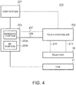
- FIG. 4 is a functional block diagram illustrating an example of the configuration of the malfunction prevention system 200.
- the malfunction prevention system 200 contains a host system 201, the electromagnetic coupling NFC module 203, the touch controller 205, the touchpad 19, and the NFC coil 21.
- the host system 201 contains hardware, such as a CPU, a system memory, a chip set, and a secondary memory, and software, such as a device driver, an OS, and an application program.
- the host system 201 can operate based on the coordinates of the touch controller 205 as an input.
- the host system 201 can exchange digital data with the NFC module 203 to communicate with the NFC card 53.
- the NFC module 203 contains a baseband portion 203a and an RF portion 203b.
- the baseband portion 203a processes a baseband signal before modulation received from the host system and a baseband signal after demodulation received from the RF portion 203b.
- the RF portion modulates carrier waves with a baseband signal in transmission and demodulates subcarrier waves to a baseband signal in reception.
- the NFC module 203 serves as an initiator to enable passive communication with the NFC card 53 having no built-in power supply.
- the NFC module 203 emits the alternating magnetic fluxes 31 from the NFC coil 21 only at specific timing when a power supply is turned on. The timing of the emission of the alternating magnetic fluxes 31 is described with reference to FIG. 6 .
- the NFC module 203 directly outputs a transmission signal to the touch controller 205 through a hardware line 207 while emitting the alternating magnetic fluxes 31 from the NFC coil 21.
- the transmission signal is used in order to change a threshold value at which the touch controller 205 detects a finger synchronously with the time when the NFC module 203 is emitting the alternating magnetic fluxes 31. Therefore, the transmission signal needs to be free from delay. Since the hardware line 207 can transmit a signal without the involvement of a device driver and a firmware executed by the CPU, the transmission signal can be transmitted without being affected by the operation of the CPU even in a pre-polling mode (see the explanation of FIG. 6 ) in which the cycle of emitting the alternating magnetic fluxes is short.
- the NFC module 203 directly outputs a disable signal showing that the NFC module 203 enters a communication mode to the touch controller 205 through the same hardware line 209.
- the disable signal is used in order for the touch controller 205 to stop the detection of a finger or to stop the output of detected coordinates.
- the hardware line 209 can also be used with the hardware line 207. The usage of the transmission signal and the disable signal is described with reference to the flow chart of FIG. 5 .
- the touchpad 19 has the plurality of electrodes arranged in the X direction and in the Y direction in order to detect the approach of a finger.
- the parasitic capacitance of a human body is added to the electrodes which the finger approaches.
- the touchpad 19 detects the approach of a finger either as changes in the self-capacitance of the electrodes or changes in the mutual capacitance between adjacent electrodes.
- the touchpad 19 may support multi-touch in which the touch of a finger is detected simultaneously at a plurality of places.
- the touch controller 205 is connected to the electrodes of the touchpad 19 by a drive circuit 211 and a sense circuit 213.
- the principle that the touch controller 205 detects the coordinates of a finger does not need to be particularly limited.
- the touch controller 205 can detect the approach of a finger from the size of the physical quantity of the sense circuit 213 responding to an alternating voltage or a pulse voltage applied to the touchpad 19 through the drive circuit 211.
- the physical quantity (detected physical quantity) for use in the detection of a finger can be any one of the charge time, the voltage, the current, or those substituting the size of the parasitic capacitance, such as the size of the capacitance, of a capacitor.
- the touch controller 205 recognizes a finger and specifies the coordinates, for example.
- An induced voltage is induced in the electrodes of the touchpad 19 due to the alternating magnetic fluxes 31 emitted by the NFC coil 21.
- the induced voltage contains various frequency components and enters, as a noise, the touch controller 205 from the sense circuit 213.
- the touch controller 205 recognizes the noise as the detected physical quantity.
- the touch controller 205 recognizes the noise as a finger.
- the level of the detected physical quantity generated by the noise is smaller than the level of the detected physical quantity generated by the finger. Therefore, when the threshold value is increased, the probability of recognizing the noise as a finger decreases but the probability of recognizing a finger simultaneously also decreases. It takes time and effort to specify the level of the detected physical quantity of the noise and the level of the detected physical quantity which causes no troubles in the detection of a finger, and then set a threshold value therebetween because the conditions vary in each laptop.
- the threshold value to the detected physical quantity is equivalent to a value determining whether the level (high or low) of the detection sensitivity of a finger is high or low. Depending on a system, the detection sensitivity decreases as the threshold value is lower but any case may be acceptable.
- the touch controller 205 changes the threshold value so as to reduce the detection sensitivity only when receiving a transmission signal through the hardware line 207. Due to the reduction in the detection sensitivity, the detection performance of a finger temporarily decreases but the noise resistance increases.
- FIG. 5 is a flow chart illustrating an operation of the malfunction prevention system 200.
- FIG. 6 is a view for explaining a state where the NFC coil 21 emits the alternating magnetic fluxes 31.
- the NFC module 203 and the touch controller 205 operate.
- the touch controller 205 sets the threshold value to the detected physical quantity as the reference threshold value at which a finger is detected without considering the influence of the NFC.
- the NFC module 203 operates as a polling device and waits the approach of the NFC card 53 operating as a listening device.
- the NFC card 53 does not transmit a signal to the NFC module 203 as an initiator when the NFC card 53 approaches the touchpad 19, and therefore the NFC module 203 needs to detect the approach of the NFC card 53 at arbitrary timing.
- the NFC module 203 may be configured so as to always emit the alternating magnetic fluxes 31 for use in communication and wait the response from the NFC card 53. However, in order to reduce the power consumption of the laptop 10 until the NFC card 53 approaches, alternating magnetic fluxes for searching are emitted from the NFC coil 21.
- Alternating magnetic fluxes 31a are equivalent to carrier waves or magnetic fluxes of the other frequencies emitted from the NFC coil 21 at a short time interval only for a short period of time. Since the NFC module 203 may operate the RF portion 203b only when emitting magnetic fluxes, the standby power can be reduced. The NFC module 203 outputs a transmission signal through the hardware line 207 at the timing of starting the emission of the alternating magnetic fluxes 31a and stops the transmission signal at the timing of stopping the emission.
- a hand holding the NFC card 53 sometimes approaches the touchpad 19 in order to perform the NFC or a hand holding a metal pen sometimes approaches the touchpad 19 in order to operate the touchpad 19.
- the alternating magnetic fluxes 31a are interlinked to the NFC coil 51 or the metal pen, an eddy current flows into the metal, and then the eddy current emits alternating magnetic fluxes.
- the NFC module 203 detects the fact that a metal approaches the vicinity of the NFC coil 21 from the frequency, the amplitude, the phase, and the like of a voltage of the NFC coil 21 interlinked to the alternating magnetic fluxes emitted from the eddy current, while emitting the alternating magnetic fluxes 31a.
- Such an operation of the NFC module 203 is referred to as a pre-polling mode.
- the touch controller 205 increases the detection threshold value at the timing of receiving a transmission signal and returns the detection threshold value to a reference threshold value at the timing when the transmission signal is stopped. Therefore, even when a noise enters a sense detection circuit 213 due to the alternating magnetic fluxes 31a emitted from the NFC coil 21, the probability of recognizing the noise as a finger decreases in the touch controller 205 and the touch controller 205 can detect a finger actually contacting the same. Moreover, the alternating magnetic fluxes 31a do not need to be weakened, and therefore, with respect to the NFC module 203, the mounting position of the NFC coil 21 can be secured directly under the touchpad 19 while not affecting the NFC.
- the pre-polling is performed even in the time zone when the NFC card 53 does not approach.
- a user needs to use the touchpad 19 during the pre-polling mode.
- the touchpad 19 cannot be used.
- the threshold value is merely increased, and therefore both the prevention of a malfunction and the detection of a finger by a noise can be achieved.
- the NFC module 203 cannot distinguish between the NFC coil 51 and the metal pen in the pre-polling but can presume the approach of the NFC coil 51.
- the NFC module 203 detecting a metal in Block 307 emits alternating magnetic fluxes 31b for a longer period of time than that of the alternating magnetic fluxes 31a from the NFC coil 21 to recognize the NFC coil 51.
- the NFC card 53 does not need to operate with the electric power received from the NFC coil 51.
- the NFC module 203 judges the approach of the NFC card 53 from the magnetic fluxes emitted from a current flowing through the NFC coil 51. Such an operation of the NFC module 203 is referred to as full-polling mode.
- the touch controller 205 increases the detection threshold value at the timing of receiving a transmission signal and returns the detection threshold value to the reference threshold value at the timing when the transmission signal is stopped.
- Block 311 when the NFC module 203 presumes the approach of the NFC card 53, the process shifts to Block 313. Unless the NFC module 203 can presume the approach of the NFC card 53 in predetermined period of time, the process returns to Block 305.
- the NFC module 203 operates as an initiator to emit alternating magnetic fluxes 31c and the NFC card 53 receives electric power from the alternating magnetic fluxes 31c to operate as a target.
- the NFC card 53 acquires electric power from a voltage induced in the NFC coil 51 to operate an IC chip 55.
- the NFC module 203 modulates carrier waves to transmit request data and the NFC card 53 load-modulate subcarrier waves to return response data from the NFC coil 51.
- the NFC module 203 acquires the response data from changes in the amplitude and the phase of the voltage of the NFC coil 21.
- Such an operation of the NFC module 203 is referred to as a communication mode.
- the NFC card 53 approaches or contacts the surface of the touchpad 19. Moreover, a finger holding the NFC card 53 approaches or contacts the touchpad 19. Also in the communication mode, there is a possibility that unintended finger coordinates are detected only by increasing the threshold value as with the pre-polling mode or the full-polling mode. In the communication mode, it is not necessary to assume that a user uses the touchpad 19.
- a disable signal is output through the hardware line 209.
- the touch controller 205 receiving the disable signal stops the coordinate detection operation to the touchpad 19.
- the touch controller 205 may be configured so as not to output detected coordinates to the host system 201.
- Block 317 when the communication mode ends, the NFC module 203 stops the disable signal, and then the process returns to Block 303.
- the full-polling mode may be omitted.
- the order from Block 301 to Block 305 varies depending on systems, and therefore is not particularly limited.
- a disable signal is transmitted through the hardware line 209 in the communication mode, a configuration may be acceptable in which the NFC module 203 transmits a disable signal to the host system 201, and the host system 201 cancels received coordinates also in the communication mode.
- the description is given taking the electromagnetic coupling wireless communication as an example, the present invention is also applicable to wireless communication using electromagnetic waves.
- FIG. 7 is a perspective view of a dual screen type electronic device 400 according to another embodiment.
- a top chassis 401 and a bottom chassis 405 are bonded by a hinge mechanism.
- the top chassis 401 contains a touch screen 403 and the bottom chassis 405 contains a touch screen 407.
- the electronic device 400 can be used in a plurality of use modes by changing the relative attitude of the top chassis 401 and the bottom chassis 405 and the attitude to the desk upper surface, as necessary, by the hinge mechanism.
- a software keyboard is displayed on the touch screen 407, whereby the electronic device 400 can be used as a laptop.
- an NFC coil 411 for communicating with the NFC card 53 is disposed under the corner of the touch screen 407.
- the touch screen 407 contains a touch panel or a touch panel function and a liquid crystal panel.
- an external type and a built-in type are mentioned.
- the touch panel is disposed on the upper surface of the liquid crystal panel.
- the built-in type an on-cell type and an in-cell type are mentioned.
- an indium tin oxide (ITO) electrode pattern is formed between a color filter substrate and a polarizing plate of the liquid crystal panel to incorporate a touch panel function therein.
- ITO indium tin oxide
- a touch panel function formed with an ITO is incorporated in pixels of a TFT array substrate of the liquid crystal panel.
- the NFC coil 411 can be disposed on these kinds of touch screen 407 by various methods. In order to emit magnetic fluxes required for the NFC to space, it is desirable to dispose the NFC coil 411 near the surface of the touch screen 407. In the external type touch screen 407, the NFC coil 411 formed with an ITO film can be disposed between the touch panel and a liquid crystal module.
- the NFC coil 411 can be formed with an ITO on a color filter substrate or in a TFT array substrate.
- a malfunction sometimes arises in the touch screen 407 due to alternating magnetic fluxes emitted by the NFC coil 411 but the malfunction can be overcome by the application of the method described with reference to FIG. 4 and FIG. 5 .
Landscapes
- Engineering & Computer Science (AREA)
- General Engineering & Computer Science (AREA)
- Theoretical Computer Science (AREA)
- Human Computer Interaction (AREA)
- Physics & Mathematics (AREA)
- General Physics & Mathematics (AREA)
- Computer Networks & Wireless Communication (AREA)
- Signal Processing (AREA)
- Near-Field Transmission Systems (AREA)
- Position Input By Displaying (AREA)
- Telephone Function (AREA)
- User Interface Of Digital Computer (AREA)
Abstract
Description
- The present invention relates to a technique of preventing a malfunction of a touch panel disposed near an antenna.
- In NFC (Near Field Communication) of a communication standard, the technical specification of which has been formulated by a standardization organization of NFC Forum, and has been specified as ISO/IEC14443 and ISO/IEC18092, communication can be performed in a state where NFC coils are brought close to each other so that the distance between the NFC coils is about 2 cm to about 4 cm or less. Some recent laptop type portable computers (laptop) support the NFC.
- Patent Document 1 discloses the invention that an electronic device having a touchpad and an antenna device prevents a wrong operation of the touchpad. Patent Document 1 describes that, when the antenna device is disposed directly under the touchpad, magnetic fluxes pass through a detection region of the touchpad in communication of the antenna device, so that the touchpad causes a malfunctions. Patent Document 2 discloses the invention of preventing a malfunction resulting from erroneous detection of a touchpad of a laptop personal computer in a closed state.
- Patent Document 2 describes that the operating system into which a predetermined code corresponding to the closed state is input disables a touchpad driver. Patent Document 3 discloses the invention that, in a liquid crystal display having an electrostatic capacity type touch panel, the influence of a noise from a liquid crystal driving device to an electrostatic capacity touch sensor is avoided. Patent Document 3 describes changing the frequency for scanning the touch sensor when a drive signal driving a liquid crystal panel varies.
- Patent Document 4 discloses the invention which enables the continuation of an input of a touch panel even when a noise from an LCD enters. Patent Document 4 describes that, when a touch panel detects an input equal to or larger than the permitted number of inputs, a voltage control program changes the γ correction curve to reduce the level of a noise generated by the LCD.
- [Patent Document 1] Japanese Patent Application Lain-Open No.
2015-32113 - [Patent Document 2] Japanese Patent Application Lain-Open No.
2014-10707 - [Patent Document 3] International Publication
WO2012/096259 - [Patent Document 4] Japanese Patent Application Lain-Open No.
2011-158936 - In the laptop, a portion directly under a touchpad is suitable for a mounting position of an NFC coil in physical aspects, such as a reduction of influence on a chassis and a measure against interference with other devices. On the other hand, it is confirmed that, when the NFC coil emits magnetic fluxes, the touchpad malfunctions due to a noise. Heretofore, various measures for preventing the malfunction have been taken. For example, the position of the NFC coil is devised or a method of interposing a ground mesh layer between the touchpad and the NFC coil is mentioned.
- The devise and the method have an effect of weakening the magnetic fluxes passing through the touchpad to lower the noise level. However, the magnetic fluxes emitted to space are also weakened, and therefore a trouble occurs in the NFC. A method in which an NFC module emits weak magnetic fluxes also similarly causes a trouble in the NFC. A method of confirming the noise detection level and the finger detection level to appropriately set a detection threshold value is mentioned. However, there is an individual difference in the mounting environment, and therefore the adjustment needs to be individually performed, which takes time and effort.
- Then, it is an object of the present invention that an electronic device having a wireless module and a touch panel prevents a malfunction of the touch panel. It is another object of the present invention to prevent a malfunction while causing no troubles in the use of a touch panel. It is a still another object of the present invention to prevent a malfunction while causing no troubles in wireless communication.
- An aspect of the present invention provides an electronic device having an electromagnetic coupling wireless module, a coil connected to the wireless module, a touch panel, and a touch controller detecting coordinates of the touch panel with predetermined detection sensitivity and reducing the detection sensitivity only while the coil is emitting magnetic fluxes. The wireless module may be one conforming to the near field communication (NFC) standard.
- Another aspect of the present invention provides an electronic device having a wireless module, an emitting element connected to the wireless module, a touch panel, and a touch controller detecting an operation to the touch panel with predetermined detection sensitivity and reducing the detection sensitivity only while the emitting element forms an electromagnetic field.
- A still another aspect of the present invention provides a method in which an electronic device having a wireless module and a touch panel prevents a malfunction of the touch panel. The touch panel detects the physical quantity which changes due to the approach of a finger with predetermined detection sensitivity and reduces the detection sensitivity in response to the emission of alternating magnetic fluxes by the wireless module. In response to the stop of the emission of the alternating magnetic fluxes, the detection sensitivity returns to the predetermined detection sensitivity.
- According to any one or all of the aspects of the present invention, the electronic device having the wireless module and the touch panel has been able to prevent a malfunction of the touch panel. Furthermore, according to any one or all of the aspects of the present invention, a malfunction has been able to be prevented while causing no troubles in the use of the touch panel. Furthermore, according to any one or all of the aspects of the present invention, a malfunction has been able to be prevented while causing no troubles in wireless communication.
-
-
FIG. 1 is a perspective view for explaining the outline of alaptop 10 supporting NFC. -
FIG. 2 is a view for explaining a state when anNFC coil 21 of thelaptop 10 and anNFC coil 51 of anNFC card 53 are electromagnetically coupled to each other. -
FIGS. 3A and 3B are a cross-sectional view and a bottom view, respectively, for explaining the mounting position of theNFC coil 21. -
FIG. 4 is a functional block diagram illustrating an example of the configuration of amalfunction prevention system 200. -
FIG. 5 is a flow chart illustrating an operation of themalfunction prevention system 200. -
FIG. 6 is a view for explaining a state where anNFC module 203 emits alternating magnetic fluxes. -
FIG. 7 is a perspective view of a dual screen typeelectronic device 400 according to another embodiment. - In most wireless communication, the energy emitted by a transmitting antenna propagates through space in the form of electromagnetic waves, and then a receiving antenna absorbs the energy from the electromagnetic waves in the space. When an alternating voltage is applied to the transmitting antenna, a high frequency current flows, so that an electric field and a magnetic field (electromagnetic field) are generated around the antenna. The electromagnetic waves for use in the wireless communication are generated so that the electric field and the magnetic field are mutually chained to propagate a long distance. Data can be transmitted while modulating the electromagnetic waves serving as carrier waves with a baseband signal.
- On the other hand, when an alternating current is caused to flow through the transmitting coil, an alternating magnetic field is generated in space close thereto. The alternating magnetic field generates alternating magnetic fluxes of a size according to the magnetic permeability of the space, and a voltage is induced due to electromagnetic induction in a receiving coil interlinked to the alternating magnetic fluxes. This phenomenon is referred to as electromagnetic induction or electromagnetic coupling and is usable for the wireless communication. When an alternating current flows through the transmitting coil, the transmitting coil also emits electromagnetic waves. However, a system of performing communication using the electromagnetic coupling of approaching coils is referred to as electromagnetic coupling wireless communication in distinction from a communication system using the electromagnetic waves.
- The electromagnetic coupling wireless communication is employed in RFID, Felica (Registered Trademark), and the like other than the NFC. The electromagnetic coupling wireless communication is also employed in wireless electric power transmission. In the electromagnetic coupling wireless communication, carrier waves serve as alternating magnetic fluxes and the communication distance falls in the range of a near magnetic field in which electromagnetic coupling can be achieved, and therefore the communication distance is short. In the electromagnetic coupling wireless communication, a large amount of alternating magnetic fluxes are generated near the transmitting coil. Therefore, when a wireless module is mounted in an electronic device, the wireless module is likely to be a noise source.
- As the NFC, passive communication in which communication is performed with a noncontact IC card in which a reader/writer does not have a power supply and active communication in which two devices each having a power supply alternately serve as an initiator and a target to perform communication are defined. In the passive communication, a polling device operating as an initiator emits strong alternating magnetic fluxes in order to supply energy to a listening device serving as a target.
-
FIG. 1 is a perspective view for explaining the outline of thelaptop 10 supporting the NFC. In thelaptop 10, adisplay chassis 11 having adisplay 13 and asystem chassis 15 having akeyboard 17 and atouchpad 19 on the surface and storing a circuit board mounting a system device therein are openably/closably coupled to each other. Under thetouchpad 19, anNFC coil 21 is disposed. - The
touchpad 19 operates a mouse cursor displayed by thedisplay 13 using a touch panel which detects a finger contacting the same to specify indicating coordinates. As thetouchpad 19, a projection type electrostatic capacity type can be used as an example and other detection principles, such as an electromagnetic induction type or a resistive film type, may be employed. In thetouchpad 19, a plurality of electrodes for detecting the position of a finger is arranged in the X direction and in the Y direction. The operation surface of thetouchpad 19 also serves an access surface of theNFC card 53. TheNFC card 53 has anNFC coil 51 and anIC chip 55. - When the
laptop 10 performs reading/writing on theNFC card 53, a user brings theNFC card 53 close to thetouchpad 19 regarded as the operation surface. Around thetouchpad 19 and thekeyboard 17, apalm rest 23 containing a metal material is provided. In theNFC coil 21, a magnetic field is weakened when a metal is present between theNFC coil 21 and theNFC card 53. A portion directly under thetouchpad 19 is suitable as the position of theNFC coil 21 in thelaptop 10, in which the chassis conditions are restricted, in terms of the fact that a good magnetic path with theNFC card 53 can be built. -
FIG. 2 is a view for explaining the state when theNFC coil 21 mounted in thelaptop 10 and theNFC coil 51 mounted in theNFC card 53 are electromagnetically coupled to each other. The NFC uses a 13.56 MHz frequency band. When a high frequency current of the use frequency band flows into theNFC coil 21, an alternating magnetic field is generated therearound, so that 13.56 MHz alternatingmagnetic fluxes 31 flow in the form of carrier waves from one side to the other side of the opening of the coil. When theNFC coil 51 approaches a position where theNFC coil 51 is interlinked to the alternatingmagnetic fluxes 31, an induction voltage is generated. The alternatingmagnetic fluxes 31 induce a voltage also in the metal present near theNFC coil 21, which causes a noise for each device. The alternatingmagnetic fluxes 31 flow while passing through thetouchpad 19, and therefore a noise is generated also in the electrodes. -
FIGS. 3A and 3B are a cross-sectional view and a bottom view, respectively, for explaining the mounting position of theNFC coil 21.FIG. 3A is a partial cross-sectional view containing thetouchpad 19 andFIG. 3B is a bottom view illustrating a state where aferrite sheet 105 is removed. On the bottom surface of thetouchpad 19, a touch controller 205 (FIG. 4 ) which detects the coordinates of the operatedtouchpad 19 and a printed circuit board (PCB) 101 on which a circuit pattern is mounted are disposed. On the lower side thePCB 101, a flexible printed circuit board (FPC) 103 on which the pattern of theNFC coil 21 is formed is disposed. TheNFC coil 21 is connected to an NFC module 203 (FIG. 4 ) with aconnector 107 mounted on thePCB 101. - On the lower side of the
FPC 103, theferrite sheet 105 for strengthening magnetic fluxes emitted by theNFC coil 21 is disposed. TheNFC coil 21 may be formed as a circuit pattern in thePCB 101. TheNFC coil 21 is disposed directly under thetouchpad 19 so that the outline is overlapped with the inner side of the projection of the outline of thetouchpad 19 or the projection, and therefore theNFC coil 21 can emit magnetic fluxes required for the NFC to the outside from the surface of thetouchpad 19. -
FIG. 4 is a functional block diagram illustrating an example of the configuration of themalfunction prevention system 200. Themalfunction prevention system 200 contains ahost system 201, the electromagneticcoupling NFC module 203, thetouch controller 205, thetouchpad 19, and theNFC coil 21. Thehost system 201 contains hardware, such as a CPU, a system memory, a chip set, and a secondary memory, and software, such as a device driver, an OS, and an application program. - The
host system 201 can operate based on the coordinates of thetouch controller 205 as an input. Thehost system 201 can exchange digital data with theNFC module 203 to communicate with theNFC card 53. TheNFC module 203 contains abaseband portion 203a and anRF portion 203b. Thebaseband portion 203a processes a baseband signal before modulation received from the host system and a baseband signal after demodulation received from theRF portion 203b. The RF portion modulates carrier waves with a baseband signal in transmission and demodulates subcarrier waves to a baseband signal in reception. - The
NFC module 203 serves as an initiator to enable passive communication with theNFC card 53 having no built-in power supply. TheNFC module 203 emits the alternatingmagnetic fluxes 31 from theNFC coil 21 only at specific timing when a power supply is turned on. The timing of the emission of the alternatingmagnetic fluxes 31 is described with reference toFIG. 6 . TheNFC module 203 directly outputs a transmission signal to thetouch controller 205 through ahardware line 207 while emitting the alternatingmagnetic fluxes 31 from theNFC coil 21. - The transmission signal is used in order to change a threshold value at which the
touch controller 205 detects a finger synchronously with the time when theNFC module 203 is emitting the alternatingmagnetic fluxes 31. Therefore, the transmission signal needs to be free from delay. Since thehardware line 207 can transmit a signal without the involvement of a device driver and a firmware executed by the CPU, the transmission signal can be transmitted without being affected by the operation of the CPU even in a pre-polling mode (see the explanation ofFIG. 6 ) in which the cycle of emitting the alternating magnetic fluxes is short. - The
NFC module 203 directly outputs a disable signal showing that theNFC module 203 enters a communication mode to thetouch controller 205 through thesame hardware line 209. The disable signal is used in order for thetouch controller 205 to stop the detection of a finger or to stop the output of detected coordinates. Thehardware line 209 can also be used with thehardware line 207. The usage of the transmission signal and the disable signal is described with reference to the flow chart ofFIG. 5 . - The
touchpad 19 has the plurality of electrodes arranged in the X direction and in the Y direction in order to detect the approach of a finger. The parasitic capacitance of a human body is added to the electrodes which the finger approaches. Thetouchpad 19 detects the approach of a finger either as changes in the self-capacitance of the electrodes or changes in the mutual capacitance between adjacent electrodes. Thetouchpad 19 may support multi-touch in which the touch of a finger is detected simultaneously at a plurality of places. - The
touch controller 205 is connected to the electrodes of thetouchpad 19 by adrive circuit 211 and asense circuit 213. In the present invention, the principle that thetouch controller 205 detects the coordinates of a finger does not need to be particularly limited. Thetouch controller 205 can detect the approach of a finger from the size of the physical quantity of thesense circuit 213 responding to an alternating voltage or a pulse voltage applied to thetouchpad 19 through thedrive circuit 211. - Herein, the physical quantity (detected physical quantity) for use in the detection of a finger can be any one of the charge time, the voltage, the current, or those substituting the size of the parasitic capacitance, such as the size of the capacitance, of a capacitor. When a threshold value is set to the detected physical quantity and the detected physical quantity exceeds the threshold value, the
touch controller 205 recognizes a finger and specifies the coordinates, for example. An induced voltage is induced in the electrodes of thetouchpad 19 due to the alternatingmagnetic fluxes 31 emitted by theNFC coil 21. The induced voltage contains various frequency components and enters, as a noise, thetouch controller 205 from thesense circuit 213. - The
touch controller 205 recognizes the noise as the detected physical quantity. When the detected physical quantity generated by the noise exceeds the threshold value, thetouch controller 205 recognizes the noise as a finger. The level of the detected physical quantity generated by the noise is smaller than the level of the detected physical quantity generated by the finger. Therefore, when the threshold value is increased, the probability of recognizing the noise as a finger decreases but the probability of recognizing a finger simultaneously also decreases. It takes time and effort to specify the level of the detected physical quantity of the noise and the level of the detected physical quantity which causes no troubles in the detection of a finger, and then set a threshold value therebetween because the conditions vary in each laptop. - The threshold value to the detected physical quantity is equivalent to a value determining whether the level (high or low) of the detection sensitivity of a finger is high or low. Depending on a system, the detection sensitivity decreases as the threshold value is lower but any case may be acceptable. The
touch controller 205 changes the threshold value so as to reduce the detection sensitivity only when receiving a transmission signal through thehardware line 207. Due to the reduction in the detection sensitivity, the detection performance of a finger temporarily decreases but the noise resistance increases. -
FIG. 5 is a flow chart illustrating an operation of themalfunction prevention system 200.FIG. 6 is a view for explaining a state where theNFC coil 21 emits the alternatingmagnetic fluxes 31. InBlock 301, theNFC module 203 and thetouch controller 205 operate. InBlock 303, thetouch controller 205 sets the threshold value to the detected physical quantity as the reference threshold value at which a finger is detected without considering the influence of the NFC. InBlock 305, theNFC module 203 operates as a polling device and waits the approach of theNFC card 53 operating as a listening device. - The
NFC card 53 does not transmit a signal to theNFC module 203 as an initiator when theNFC card 53 approaches thetouchpad 19, and therefore theNFC module 203 needs to detect the approach of theNFC card 53 at arbitrary timing. TheNFC module 203 may be configured so as to always emit the alternatingmagnetic fluxes 31 for use in communication and wait the response from theNFC card 53. However, in order to reduce the power consumption of thelaptop 10 until theNFC card 53 approaches, alternating magnetic fluxes for searching are emitted from theNFC coil 21. - Alternating
magnetic fluxes 31a (FIG. 6 ) for searching are equivalent to carrier waves or magnetic fluxes of the other frequencies emitted from theNFC coil 21 at a short time interval only for a short period of time. Since theNFC module 203 may operate theRF portion 203b only when emitting magnetic fluxes, the standby power can be reduced. TheNFC module 203 outputs a transmission signal through thehardware line 207 at the timing of starting the emission of the alternatingmagnetic fluxes 31a and stops the transmission signal at the timing of stopping the emission. - A hand holding the
NFC card 53 sometimes approaches thetouchpad 19 in order to perform the NFC or a hand holding a metal pen sometimes approaches thetouchpad 19 in order to operate thetouchpad 19. When the alternatingmagnetic fluxes 31a are interlinked to theNFC coil 51 or the metal pen, an eddy current flows into the metal, and then the eddy current emits alternating magnetic fluxes. TheNFC module 203 detects the fact that a metal approaches the vicinity of theNFC coil 21 from the frequency, the amplitude, the phase, and the like of a voltage of theNFC coil 21 interlinked to the alternating magnetic fluxes emitted from the eddy current, while emitting the alternatingmagnetic fluxes 31a. Such an operation of theNFC module 203 is referred to as a pre-polling mode. - During the pre-polling mode, the
touch controller 205 increases the detection threshold value at the timing of receiving a transmission signal and returns the detection threshold value to a reference threshold value at the timing when the transmission signal is stopped. Therefore, even when a noise enters asense detection circuit 213 due to the alternatingmagnetic fluxes 31a emitted from theNFC coil 21, the probability of recognizing the noise as a finger decreases in thetouch controller 205 and thetouch controller 205 can detect a finger actually contacting the same. Moreover, the alternatingmagnetic fluxes 31a do not need to be weakened, and therefore, with respect to theNFC module 203, the mounting position of theNFC coil 21 can be secured directly under thetouchpad 19 while not affecting the NFC. - The pre-polling is performed even in the time zone when the
NFC card 53 does not approach. A user needs to use thetouchpad 19 during the pre-polling mode. When the operation of thetouch controller 205 is stopped while theNFC module 203 is emitting the alternatingmagnetic fluxes 31a, thetouchpad 19 cannot be used. However, in this embodiment, the threshold value is merely increased, and therefore both the prevention of a malfunction and the detection of a finger by a noise can be achieved. - The
NFC module 203 cannot distinguish between theNFC coil 51 and the metal pen in the pre-polling but can presume the approach of theNFC coil 51. InBlock 309, theNFC module 203 detecting a metal inBlock 307 emits alternatingmagnetic fluxes 31b for a longer period of time than that of the alternatingmagnetic fluxes 31a from theNFC coil 21 to recognize theNFC coil 51. At this time, theNFC card 53 does not need to operate with the electric power received from theNFC coil 51. TheNFC module 203 judges the approach of theNFC card 53 from the magnetic fluxes emitted from a current flowing through theNFC coil 51. Such an operation of theNFC module 203 is referred to as full-polling mode. - During the full-polling mode, the
touch controller 205 increases the detection threshold value at the timing of receiving a transmission signal and returns the detection threshold value to the reference threshold value at the timing when the transmission signal is stopped. InBlock 311, when theNFC module 203 presumes the approach of theNFC card 53, the process shifts to Block 313. Unless theNFC module 203 can presume the approach of theNFC card 53 in predetermined period of time, the process returns to Block 305. - In
Block 313, theNFC module 203 operates as an initiator to emit alternatingmagnetic fluxes 31c and theNFC card 53 receives electric power from the alternatingmagnetic fluxes 31c to operate as a target. TheNFC card 53 acquires electric power from a voltage induced in theNFC coil 51 to operate anIC chip 55. TheNFC module 203 modulates carrier waves to transmit request data and theNFC card 53 load-modulate subcarrier waves to return response data from theNFC coil 51. TheNFC module 203 acquires the response data from changes in the amplitude and the phase of the voltage of theNFC coil 21. Such an operation of theNFC module 203 is referred to as a communication mode. - In the communication mode, the
NFC card 53 approaches or contacts the surface of thetouchpad 19. Moreover, a finger holding theNFC card 53 approaches or contacts thetouchpad 19. Also in the communication mode, there is a possibility that unintended finger coordinates are detected only by increasing the threshold value as with the pre-polling mode or the full-polling mode. In the communication mode, it is not necessary to assume that a user uses thetouchpad 19. - When the
NFC module 203 enters the communication mode, a disable signal is output through thehardware line 209. Thetouch controller 205 receiving the disable signal stops the coordinate detection operation to thetouchpad 19. Thetouch controller 205 may be configured so as not to output detected coordinates to thehost system 201. InBlock 317, when the communication mode ends, theNFC module 203 stops the disable signal, and then the process returns to Block 303. - As the configuration and the operation procedure of the
malfunction prevention system 200, one embodiment of the present invention is described and the scope of the present invention is as described in Claims. For example, the full-polling mode may be omitted. Moreover, the order fromBlock 301 toBlock 305 varies depending on systems, and therefore is not particularly limited. Although a disable signal is transmitted through thehardware line 209 in the communication mode, a configuration may be acceptable in which theNFC module 203 transmits a disable signal to thehost system 201, and thehost system 201 cancels received coordinates also in the communication mode. Moreover, although the description is given taking the electromagnetic coupling wireless communication as an example, the present invention is also applicable to wireless communication using electromagnetic waves. - The present invention is also applicable not only to malfunction prevention of a touchpad but malfunction prevention of a touch screen.
FIG. 7 is a perspective view of a dual screen typeelectronic device 400 according to another embodiment. In theelectronic device 400, atop chassis 401 and abottom chassis 405 are bonded by a hinge mechanism. Thetop chassis 401 contains atouch screen 403 and thebottom chassis 405 contains atouch screen 407. - The
electronic device 400 can be used in a plurality of use modes by changing the relative attitude of thetop chassis 401 and thebottom chassis 405 and the attitude to the desk upper surface, as necessary, by the hinge mechanism. In an example of the use mode, a software keyboard is displayed on thetouch screen 407, whereby theelectronic device 400 can be used as a laptop. Under the corner of thetouch screen 407, anNFC coil 411 for communicating with theNFC card 53 is disposed. - The
touch screen 407 contains a touch panel or a touch panel function and a liquid crystal panel. As a method for incorporating the touch panel in thetouch screen 407, an external type and a built-in type are mentioned. In the external type, the touch panel is disposed on the upper surface of the liquid crystal panel. As the built-in type, an on-cell type and an in-cell type are mentioned. In the on-cell type, an indium tin oxide (ITO) electrode pattern is formed between a color filter substrate and a polarizing plate of the liquid crystal panel to incorporate a touch panel function therein. In the in-cell type, a touch panel function formed with an ITO is incorporated in pixels of a TFT array substrate of the liquid crystal panel. - The
NFC coil 411 can be disposed on these kinds oftouch screen 407 by various methods. In order to emit magnetic fluxes required for the NFC to space, it is desirable to dispose theNFC coil 411 near the surface of thetouch screen 407. In the externaltype touch screen 407, theNFC coil 411 formed with an ITO film can be disposed between the touch panel and a liquid crystal module. - In the built-in
type touch screen 407, theNFC coil 411 can be formed with an ITO on a color filter substrate or in a TFT array substrate. In such atouch screen 407, a malfunction sometimes arises in thetouch screen 407 due to alternating magnetic fluxes emitted by theNFC coil 411 but the malfunction can be overcome by the application of the method described with reference toFIG. 4 andFIG. 5 . - The present invention is described above with reference to specific embodiments illustrated in the drawings. However, it is a matter of course that the present invention is not limited to the embodiments illustrated in the drawings and any configuration known before can be employed insofar as the effects of the present invention are demonstrated.
-
- 10
- laptop
- 19
- touchpad
- 21, 411
- NFC coil
- 31, 31a, 31b, 31c
- alternating magnetic flux
- 51
- NFC Coil
- 53
- NFC Card
- 200
- malfunction prevention system
Claims (13)
- An electronic device comprising:an electromagnetic coupling wireless module;a coil connected to the wireless module;a touch panel; anda touch controller detecting an operation to the touch panel with predetermined detection sensitivity and reducing the detection sensitivity only while the coil is emitting an alternating magnetic flux.
- The electronic device according to Claim 1, wherein the wireless module conforms to a near field communication (NFC) standard.
- The electronic device according to Claim 1, wherein the touch controller receives a transmission signal showing that the coil is emitting an alternating magnetic flux through a hardware transmission path from the wireless module.
- The electronic device according to Claim 1, wherein the touch controller reduces the detection sensitivity while the wireless module is emitting an alternating magnetic flux for searching approach of a communication target device.
- The electronic device according to Claim 4, wherein the touch controller disables an input from the touch panel while the wireless module is emitting an alternating magnetic flux for communicating with the communication target device.
- The electronic device according to Claim 1, wherein the touch panel is a touchpad operating a mouse cursor.
- The electronic device according to Claim 6, wherein the coil is disposed on a back surface of the touchpad so as to be adjacent to the touchpad.
- The electronic device according to Claim 7, wherein a projection of an outline of the touchpad is overlapped with an outline of the coil.
- The electronic device according to Claim 6, wherein the coil is formed with a pattern on a circuit board of the touchpad disposed on the back surface of the touchpad.
- The electronic device according to Claim 1, wherein the coil is incorporated in a touch screen containing a display.
- An electronic device comprising:a wireless module;an emitting element connected to the wireless module;a touch panel; anda touch controller detecting an operation to the touch panel with predetermined detection sensitivity and reducing the detection sensitivity only while the emitting element forms an electromagnetic field.
- A method in which an electronic device having a wireless module and a touchpad prevents a malfunction of the touchpad, the method comprising:detecting a physical quantity which changes due to approach of a finger with predetermined detection sensitivity by the touchpad;reducing the detection sensitivity in response to emission of an alternating magnetic flux by the wireless module; andreturning the detection sensitivity to the predetermined detection sensitivity in response to a stop of the emission of the alternating magnetic flux.
- The method according to Claim 12 comprising:emitting a first alternating magnetic flux for detecting a partner device approaching the touchpad;reducing the detection sensitivity in response to the emission of the first alternating magnetic flux;emitting a second alternating magnetic flux for communicating with the partner device; andstopping a detection function of the touchpad while the second alternating magnetic flux is being emitted.
Applications Claiming Priority (1)
| Application Number | Priority Date | Filing Date | Title |
|---|---|---|---|
| JP2016125031A JP6193450B1 (en) | 2016-06-24 | 2016-06-24 | Electronic device for preventing malfunction of touch panel and method for preventing malfunction |
Publications (2)
| Publication Number | Publication Date |
|---|---|
| EP3260959A1 true EP3260959A1 (en) | 2017-12-27 |
| EP3260959B1 EP3260959B1 (en) | 2019-03-20 |
Family
ID=59061913
Family Applications (1)
| Application Number | Title | Priority Date | Filing Date |
|---|---|---|---|
| EP17176016.8A Active EP3260959B1 (en) | 2016-06-24 | 2017-06-14 | Electronic device preventing malfunction of touch panel and malfunction prevention method |
Country Status (6)
| Country | Link |
|---|---|
| US (1) | US10394380B2 (en) |
| EP (1) | EP3260959B1 (en) |
| JP (1) | JP6193450B1 (en) |
| CN (1) | CN107544689B (en) |
| DE (1) | DE102017111383A1 (en) |
| GB (1) | GB2551903B (en) |
Families Citing this family (13)
| Publication number | Priority date | Publication date | Assignee | Title |
|---|---|---|---|---|
| CN105224136B (en) * | 2015-10-13 | 2018-02-23 | 京东方科技集团股份有限公司 | A kind of touch-control display panel and preparation method thereof, driving method, display device |
| CN108768491B (en) * | 2018-07-03 | 2021-07-27 | 成都博士信智能科技发展有限公司 | Submersible communication system and method |
| KR102260916B1 (en) * | 2018-07-17 | 2021-06-04 | 주식회사 아하정보통신 | Touch sensor using PCAP and EMR method using copper mesh |
| CN110737343B (en) * | 2018-07-18 | 2024-07-26 | 北京小米移动软件有限公司 | Anti-false touch method and device of electronic equipment, electronic equipment and storage medium |
| JP2020017787A (en) * | 2018-07-23 | 2020-01-30 | レノボ・シンガポール・プライベート・リミテッド | Electronic device, electronic component, control method, and program |
| US11409972B2 (en) * | 2018-09-14 | 2022-08-09 | Apple Inc. | Coexistence of wireless technologies on an antenna |
| EP3859526A1 (en) * | 2020-01-30 | 2021-08-04 | Hewlett-Packard Development Company, L.P. | Error information storage |
| CN217426089U (en) * | 2021-12-10 | 2022-09-13 | 敦泰电子(深圳)有限公司 | Notebook computer and near field communication system |
| JP7122709B1 (en) | 2022-02-02 | 2022-08-22 | パナソニックIpマネジメント株式会社 | ELECTRONIC DEVICE AND METHOD OF CONTROLLING ELECTRONIC DEVICE |
| JP7434413B2 (en) | 2022-05-23 | 2024-02-20 | レノボ・シンガポール・プライベート・リミテッド | Electronic equipment and control methods |
| JP7417883B1 (en) | 2023-04-12 | 2024-01-19 | パナソニックIpマネジメント株式会社 | Electronic devices and control methods for electronic devices |
| CN120917413A (en) | 2023-04-13 | 2025-11-07 | 三星电子株式会社 | Electronic device for controlling touch sensitivity based on radar and operating method thereof |
| CN119493492A (en) * | 2024-09-20 | 2025-02-21 | 深圳市新国都支付技术有限公司 | A method, system and device for adjusting field intensity of touch screen in touch state |
Citations (8)
| Publication number | Priority date | Publication date | Assignee | Title |
|---|---|---|---|---|
| JP2011158936A (en) | 2010-01-29 | 2011-08-18 | Lenovo Singapore Pte Ltd | Touch panel system aiming at reduction of electromagnetic noise |
| WO2012096259A1 (en) | 2011-01-14 | 2012-07-19 | シャープ株式会社 | Liquid crystal display device and drive method therefor |
| JP2014010707A (en) | 2012-06-29 | 2014-01-20 | Nec Personal Computers Ltd | Information processing apparatus |
| US20140078094A1 (en) * | 2012-09-14 | 2014-03-20 | Songnan Yang | Co-existence of touch sensor and nfc antenna |
| US20140253963A1 (en) * | 2013-03-05 | 2014-09-11 | Brother Kogyo Kabushiki Kaisha | Communication device and non-transitory computer-readable storage medium storing program for controlling the communication device |
| WO2014189824A1 (en) * | 2013-05-20 | 2014-11-27 | Google Inc. | Touch scanning and wireless scanning in a portable computing device |
| JP2015032113A (en) | 2013-08-01 | 2015-02-16 | Necトーキン株式会社 | Electronic device |
| JP2016024746A (en) * | 2014-07-24 | 2016-02-08 | レノボ・シンガポール・プライベート・リミテッド | Method, electronic apparatus, and computer program that make touch operation for radio communication easy |
Family Cites Families (8)
| Publication number | Priority date | Publication date | Assignee | Title |
|---|---|---|---|---|
| JPH11353432A (en) * | 1998-06-04 | 1999-12-24 | Nippon Electric Ind Co Ltd | Ic card reader and writer |
| US6380930B1 (en) * | 1999-03-09 | 2002-04-30 | K-Tech Devices Corporation | Laptop touchpad with integrated antenna |
| JP2006195925A (en) * | 2005-01-17 | 2006-07-27 | Nippon Signal Co Ltd:The | Touch panel device |
| JP2012178091A (en) * | 2011-02-28 | 2012-09-13 | Nec Casio Mobile Communications Ltd | Input device, input control method and program |
| US9030421B2 (en) * | 2011-04-01 | 2015-05-12 | Qualcomm Incorporated | Touchscreen controller with adjustable parameters |
| CN104123041B (en) * | 2014-07-23 | 2017-06-16 | 上海天马微电子有限公司 | Display device and driving method thereof |
| JP6378037B2 (en) * | 2014-10-17 | 2018-08-22 | マクセルホールディングス株式会社 | Portable device, contactless charging support method, and contactless charging support program |
| WO2016118901A1 (en) * | 2015-01-22 | 2016-07-28 | Texas Tech University System | System and method for non-contact interaction with mobile devices |
-
2016
- 2016-06-24 JP JP2016125031A patent/JP6193450B1/en active Active
-
2017
- 2017-03-30 CN CN201710202245.6A patent/CN107544689B/en active Active
- 2017-05-24 DE DE102017111383.5A patent/DE102017111383A1/en active Pending
- 2017-05-24 GB GB1708286.8A patent/GB2551903B/en active Active
- 2017-06-14 EP EP17176016.8A patent/EP3260959B1/en active Active
- 2017-06-23 US US15/631,719 patent/US10394380B2/en active Active
Patent Citations (8)
| Publication number | Priority date | Publication date | Assignee | Title |
|---|---|---|---|---|
| JP2011158936A (en) | 2010-01-29 | 2011-08-18 | Lenovo Singapore Pte Ltd | Touch panel system aiming at reduction of electromagnetic noise |
| WO2012096259A1 (en) | 2011-01-14 | 2012-07-19 | シャープ株式会社 | Liquid crystal display device and drive method therefor |
| JP2014010707A (en) | 2012-06-29 | 2014-01-20 | Nec Personal Computers Ltd | Information processing apparatus |
| US20140078094A1 (en) * | 2012-09-14 | 2014-03-20 | Songnan Yang | Co-existence of touch sensor and nfc antenna |
| US20140253963A1 (en) * | 2013-03-05 | 2014-09-11 | Brother Kogyo Kabushiki Kaisha | Communication device and non-transitory computer-readable storage medium storing program for controlling the communication device |
| WO2014189824A1 (en) * | 2013-05-20 | 2014-11-27 | Google Inc. | Touch scanning and wireless scanning in a portable computing device |
| JP2015032113A (en) | 2013-08-01 | 2015-02-16 | Necトーキン株式会社 | Electronic device |
| JP2016024746A (en) * | 2014-07-24 | 2016-02-08 | レノボ・シンガポール・プライベート・リミテッド | Method, electronic apparatus, and computer program that make touch operation for radio communication easy |
Also Published As
| Publication number | Publication date |
|---|---|
| CN107544689A (en) | 2018-01-05 |
| JP2017228173A (en) | 2017-12-28 |
| GB201708286D0 (en) | 2017-07-05 |
| JP6193450B1 (en) | 2017-09-06 |
| US20170371491A1 (en) | 2017-12-28 |
| US10394380B2 (en) | 2019-08-27 |
| GB2551903A (en) | 2018-01-03 |
| GB2551903B (en) | 2019-10-30 |
| DE102017111383A1 (en) | 2017-12-28 |
| EP3260959B1 (en) | 2019-03-20 |
| CN107544689B (en) | 2021-01-15 |
Similar Documents
| Publication | Publication Date | Title |
|---|---|---|
| EP3260959B1 (en) | Electronic device preventing malfunction of touch panel and malfunction prevention method | |
| US12346517B2 (en) | Electronic device and control method therefor | |
| RU2609095C2 (en) | Hybrid touch screen device and method for operating same | |
| US8564553B2 (en) | Electronic stylus, capacitive touchpad module, and apparatus for touch input | |
| US8922525B2 (en) | Touch-controlled electronic device and method for reducing wireless signal interference to touch sensing function | |
| US20150355708A1 (en) | Touch communications device for detecting relative movement status of object close to, or in contact with, touch panel and related movement detection method | |
| CN103389804B (en) | Coordinate instruction equipment and the coordinate measurment instrument for measuring its input position | |
| CN104485983A (en) | Touch screen and terminal integrated with NFC (Near Filed Communication) antenna and near filed communication method thereof | |
| US11941199B2 (en) | Electronic apparatus and method of controlling electronic apparatus | |
| US20200026379A1 (en) | Near field communication management | |
| US20150213783A1 (en) | Touch electronic device and touch link method | |
| US11687188B2 (en) | Input device with near-field communication | |
| JP7372403B1 (en) | Electronic equipment and control method | |
| CN112860098A (en) | Electronic device | |
| JP3904939B2 (en) | Card status detection device | |
| US9939947B2 (en) | Touch communications device with multiple partial firmwares and related method | |
| US11995276B2 (en) | Touch sensitive structure and touch sensitive processing apparatus, method and electronic system thereof | |
| EP2899895A1 (en) | Electronic devices, near field communication methods and near field communication systems |
Legal Events
| Date | Code | Title | Description |
|---|---|---|---|
| STAA | Information on the status of an ep patent application or granted ep patent |
Free format text: STATUS: EXAMINATION IS IN PROGRESS |
|
| PUAI | Public reference made under article 153(3) epc to a published international application that has entered the european phase |
Free format text: ORIGINAL CODE: 0009012 |
|
| 17P | Request for examination filed |
Effective date: 20170614 |
|
| AK | Designated contracting states |
Kind code of ref document: A1 Designated state(s): AL AT BE BG CH CY CZ DE DK EE ES FI FR GB GR HR HU IE IS IT LI LT LU LV MC MK MT NL NO PL PT RO RS SE SI SK SM TR |
|
| AX | Request for extension of the european patent |
Extension state: BA ME |
|
| RIN1 | Information on inventor provided before grant (corrected) |
Inventor name: KITAMURA, MASAHIRO Inventor name: HORIKOSHI, HIDETO Inventor name: HORIUCHI, MITSUO Inventor name: CHUJO, HIDEKAZU |
|
| REG | Reference to a national code |
Ref country code: DE Ref legal event code: R079 Ref document number: 602017002786 Country of ref document: DE Free format text: PREVIOUS MAIN CLASS: G06F0003041000 Ipc: H04B0005000000 |
|
| GRAP | Despatch of communication of intention to grant a patent |
Free format text: ORIGINAL CODE: EPIDOSNIGR1 |
|
| STAA | Information on the status of an ep patent application or granted ep patent |
Free format text: STATUS: GRANT OF PATENT IS INTENDED |
|
| RIC1 | Information provided on ipc code assigned before grant |
Ipc: G06F 3/041 20060101ALI20181031BHEP Ipc: H04B 5/00 20060101AFI20181031BHEP Ipc: G06F 3/0354 20130101ALI20181031BHEP |
|
| INTG | Intention to grant announced |
Effective date: 20181204 |
|
| RIN1 | Information on inventor provided before grant (corrected) |
Inventor name: HORIKOSHI, HIDETO Inventor name: CHUJO, HIDEKAZU Inventor name: KITAMURA, MASAHIRO Inventor name: HORIUCHI, MITSUO |
|
| GRAS | Grant fee paid |
Free format text: ORIGINAL CODE: EPIDOSNIGR3 |
|
| GRAA | (expected) grant |
Free format text: ORIGINAL CODE: 0009210 |
|
| STAA | Information on the status of an ep patent application or granted ep patent |
Free format text: STATUS: THE PATENT HAS BEEN GRANTED |
|
| AK | Designated contracting states |
Kind code of ref document: B1 Designated state(s): AL AT BE BG CH CY CZ DE DK EE ES FI FR GB GR HR HU IE IS IT LI LT LU LV MC MK MT NL NO PL PT RO RS SE SI SK SM TR |
|
| REG | Reference to a national code |
Ref country code: GB Ref legal event code: FG4D |
|
| REG | Reference to a national code |
Ref country code: CH Ref legal event code: EP |
|
| REG | Reference to a national code |
Ref country code: DE Ref legal event code: R096 Ref document number: 602017002786 Country of ref document: DE |
|
| REG | Reference to a national code |
Ref country code: AT Ref legal event code: REF Ref document number: 1111573 Country of ref document: AT Kind code of ref document: T Effective date: 20190415 |
|
| REG | Reference to a national code |
Ref country code: IE Ref legal event code: FG4D |
|
| REG | Reference to a national code |
Ref country code: NL Ref legal event code: FP |
|
| PG25 | Lapsed in a contracting state [announced via postgrant information from national office to epo] |
Ref country code: SE Free format text: LAPSE BECAUSE OF FAILURE TO SUBMIT A TRANSLATION OF THE DESCRIPTION OR TO PAY THE FEE WITHIN THE PRESCRIBED TIME-LIMIT Effective date: 20190320 Ref country code: LT Free format text: LAPSE BECAUSE OF FAILURE TO SUBMIT A TRANSLATION OF THE DESCRIPTION OR TO PAY THE FEE WITHIN THE PRESCRIBED TIME-LIMIT Effective date: 20190320 Ref country code: NO Free format text: LAPSE BECAUSE OF FAILURE TO SUBMIT A TRANSLATION OF THE DESCRIPTION OR TO PAY THE FEE WITHIN THE PRESCRIBED TIME-LIMIT Effective date: 20190620 Ref country code: FI Free format text: LAPSE BECAUSE OF FAILURE TO SUBMIT A TRANSLATION OF THE DESCRIPTION OR TO PAY THE FEE WITHIN THE PRESCRIBED TIME-LIMIT Effective date: 20190320 |
|
| REG | Reference to a national code |
Ref country code: LT Ref legal event code: MG4D |
|
| PG25 | Lapsed in a contracting state [announced via postgrant information from national office to epo] |
Ref country code: BG Free format text: LAPSE BECAUSE OF FAILURE TO SUBMIT A TRANSLATION OF THE DESCRIPTION OR TO PAY THE FEE WITHIN THE PRESCRIBED TIME-LIMIT Effective date: 20190620 Ref country code: RS Free format text: LAPSE BECAUSE OF FAILURE TO SUBMIT A TRANSLATION OF THE DESCRIPTION OR TO PAY THE FEE WITHIN THE PRESCRIBED TIME-LIMIT Effective date: 20190320 Ref country code: LV Free format text: LAPSE BECAUSE OF FAILURE TO SUBMIT A TRANSLATION OF THE DESCRIPTION OR TO PAY THE FEE WITHIN THE PRESCRIBED TIME-LIMIT Effective date: 20190320 Ref country code: GR Free format text: LAPSE BECAUSE OF FAILURE TO SUBMIT A TRANSLATION OF THE DESCRIPTION OR TO PAY THE FEE WITHIN THE PRESCRIBED TIME-LIMIT Effective date: 20190621 Ref country code: HR Free format text: LAPSE BECAUSE OF FAILURE TO SUBMIT A TRANSLATION OF THE DESCRIPTION OR TO PAY THE FEE WITHIN THE PRESCRIBED TIME-LIMIT Effective date: 20190320 |
|
| REG | Reference to a national code |
Ref country code: AT Ref legal event code: MK05 Ref document number: 1111573 Country of ref document: AT Kind code of ref document: T Effective date: 20190320 |
|
| PG25 | Lapsed in a contracting state [announced via postgrant information from national office to epo] |
Ref country code: IT Free format text: LAPSE BECAUSE OF FAILURE TO SUBMIT A TRANSLATION OF THE DESCRIPTION OR TO PAY THE FEE WITHIN THE PRESCRIBED TIME-LIMIT Effective date: 20190320 Ref country code: SK Free format text: LAPSE BECAUSE OF FAILURE TO SUBMIT A TRANSLATION OF THE DESCRIPTION OR TO PAY THE FEE WITHIN THE PRESCRIBED TIME-LIMIT Effective date: 20190320 Ref country code: AL Free format text: LAPSE BECAUSE OF FAILURE TO SUBMIT A TRANSLATION OF THE DESCRIPTION OR TO PAY THE FEE WITHIN THE PRESCRIBED TIME-LIMIT Effective date: 20190320 Ref country code: PT Free format text: LAPSE BECAUSE OF FAILURE TO SUBMIT A TRANSLATION OF THE DESCRIPTION OR TO PAY THE FEE WITHIN THE PRESCRIBED TIME-LIMIT Effective date: 20190720 Ref country code: EE Free format text: LAPSE BECAUSE OF FAILURE TO SUBMIT A TRANSLATION OF THE DESCRIPTION OR TO PAY THE FEE WITHIN THE PRESCRIBED TIME-LIMIT Effective date: 20190320 Ref country code: ES Free format text: LAPSE BECAUSE OF FAILURE TO SUBMIT A TRANSLATION OF THE DESCRIPTION OR TO PAY THE FEE WITHIN THE PRESCRIBED TIME-LIMIT Effective date: 20190320 Ref country code: CZ Free format text: LAPSE BECAUSE OF FAILURE TO SUBMIT A TRANSLATION OF THE DESCRIPTION OR TO PAY THE FEE WITHIN THE PRESCRIBED TIME-LIMIT Effective date: 20190320 Ref country code: RO Free format text: LAPSE BECAUSE OF FAILURE TO SUBMIT A TRANSLATION OF THE DESCRIPTION OR TO PAY THE FEE WITHIN THE PRESCRIBED TIME-LIMIT Effective date: 20190320 |
|
| PG25 | Lapsed in a contracting state [announced via postgrant information from national office to epo] |
Ref country code: SM Free format text: LAPSE BECAUSE OF FAILURE TO SUBMIT A TRANSLATION OF THE DESCRIPTION OR TO PAY THE FEE WITHIN THE PRESCRIBED TIME-LIMIT Effective date: 20190320 Ref country code: PL Free format text: LAPSE BECAUSE OF FAILURE TO SUBMIT A TRANSLATION OF THE DESCRIPTION OR TO PAY THE FEE WITHIN THE PRESCRIBED TIME-LIMIT Effective date: 20190320 |
|
| PG25 | Lapsed in a contracting state [announced via postgrant information from national office to epo] |
Ref country code: IS Free format text: LAPSE BECAUSE OF FAILURE TO SUBMIT A TRANSLATION OF THE DESCRIPTION OR TO PAY THE FEE WITHIN THE PRESCRIBED TIME-LIMIT Effective date: 20190720 Ref country code: AT Free format text: LAPSE BECAUSE OF FAILURE TO SUBMIT A TRANSLATION OF THE DESCRIPTION OR TO PAY THE FEE WITHIN THE PRESCRIBED TIME-LIMIT Effective date: 20190320 |
|
| REG | Reference to a national code |
Ref country code: DE Ref legal event code: R097 Ref document number: 602017002786 Country of ref document: DE |
|
| PLBE | No opposition filed within time limit |
Free format text: ORIGINAL CODE: 0009261 |
|
| STAA | Information on the status of an ep patent application or granted ep patent |
Free format text: STATUS: NO OPPOSITION FILED WITHIN TIME LIMIT |
|
| REG | Reference to a national code |
Ref country code: DE Ref legal event code: R082 Ref document number: 602017002786 Country of ref document: DE Representative=s name: SCHWEIGER & PARTNERS, DE Ref country code: DE Ref legal event code: R081 Ref document number: 602017002786 Country of ref document: DE Owner name: LENOVO PC INTERNATIONAL LIMITED, HK Free format text: FORMER OWNER: LENOVO (SINGAPORE) PTE. LTD., SINGAPORE, SG |
|
| PG25 | Lapsed in a contracting state [announced via postgrant information from national office to epo] |
Ref country code: MC Free format text: LAPSE BECAUSE OF FAILURE TO SUBMIT A TRANSLATION OF THE DESCRIPTION OR TO PAY THE FEE WITHIN THE PRESCRIBED TIME-LIMIT Effective date: 20190320 Ref country code: DK Free format text: LAPSE BECAUSE OF FAILURE TO SUBMIT A TRANSLATION OF THE DESCRIPTION OR TO PAY THE FEE WITHIN THE PRESCRIBED TIME-LIMIT Effective date: 20190320 |
|
| 26N | No opposition filed |
Effective date: 20200102 |
|
| PG25 | Lapsed in a contracting state [announced via postgrant information from national office to epo] |
Ref country code: SI Free format text: LAPSE BECAUSE OF FAILURE TO SUBMIT A TRANSLATION OF THE DESCRIPTION OR TO PAY THE FEE WITHIN THE PRESCRIBED TIME-LIMIT Effective date: 20190320 |
|
| REG | Reference to a national code |
Ref country code: BE Ref legal event code: PD Owner name: LENOVO PC INTERNATIONAL LIMITED; HK Free format text: DETAILS ASSIGNMENT: CHANGE OF OWNER(S), CESSION; FORMER OWNER NAME: LENOVO (SINGAPORE) PTE. LTD. Effective date: 20191205 |
|
| PG25 | Lapsed in a contracting state [announced via postgrant information from national office to epo] |
Ref country code: TR Free format text: LAPSE BECAUSE OF FAILURE TO SUBMIT A TRANSLATION OF THE DESCRIPTION OR TO PAY THE FEE WITHIN THE PRESCRIBED TIME-LIMIT Effective date: 20190320 |
|
| PG25 | Lapsed in a contracting state [announced via postgrant information from national office to epo] |
Ref country code: IE Free format text: LAPSE BECAUSE OF NON-PAYMENT OF DUE FEES Effective date: 20190614 |
|
| REG | Reference to a national code |
Ref country code: GB Ref legal event code: 732E Free format text: REGISTERED BETWEEN 20200416 AND 20200422 |
|
| PG25 | Lapsed in a contracting state [announced via postgrant information from national office to epo] |
Ref country code: LU Free format text: LAPSE BECAUSE OF NON-PAYMENT OF DUE FEES Effective date: 20190614 |
|
| PG25 | Lapsed in a contracting state [announced via postgrant information from national office to epo] |
Ref country code: FR Free format text: LAPSE BECAUSE OF NON-PAYMENT OF DUE FEES Effective date: 20190630 |
|
| REG | Reference to a national code |
Ref country code: CH Ref legal event code: PL |
|
| PG25 | Lapsed in a contracting state [announced via postgrant information from national office to epo] |
Ref country code: CH Free format text: LAPSE BECAUSE OF NON-PAYMENT OF DUE FEES Effective date: 20200630 Ref country code: LI Free format text: LAPSE BECAUSE OF NON-PAYMENT OF DUE FEES Effective date: 20200630 |
|
| PG25 | Lapsed in a contracting state [announced via postgrant information from national office to epo] |
Ref country code: CY Free format text: LAPSE BECAUSE OF FAILURE TO SUBMIT A TRANSLATION OF THE DESCRIPTION OR TO PAY THE FEE WITHIN THE PRESCRIBED TIME-LIMIT Effective date: 20190320 |
|
| PG25 | Lapsed in a contracting state [announced via postgrant information from national office to epo] |
Ref country code: MT Free format text: LAPSE BECAUSE OF FAILURE TO SUBMIT A TRANSLATION OF THE DESCRIPTION OR TO PAY THE FEE WITHIN THE PRESCRIBED TIME-LIMIT Effective date: 20190320 Ref country code: HU Free format text: LAPSE BECAUSE OF FAILURE TO SUBMIT A TRANSLATION OF THE DESCRIPTION OR TO PAY THE FEE WITHIN THE PRESCRIBED TIME-LIMIT; INVALID AB INITIO Effective date: 20170614 |
|
| PG25 | Lapsed in a contracting state [announced via postgrant information from national office to epo] |
Ref country code: MK Free format text: LAPSE BECAUSE OF FAILURE TO SUBMIT A TRANSLATION OF THE DESCRIPTION OR TO PAY THE FEE WITHIN THE PRESCRIBED TIME-LIMIT Effective date: 20190320 |
|
| REG | Reference to a national code |
Ref country code: DE Ref legal event code: R082 Ref document number: 602017002786 Country of ref document: DE Representative=s name: SCHWEIGER, MARTIN, DIPL.-ING. UNIV., DE |
|
| P01 | Opt-out of the competence of the unified patent court (upc) registered |
Effective date: 20230627 |
|
| REG | Reference to a national code |
Ref country code: GB Ref legal event code: 732E Free format text: REGISTERED BETWEEN 20250508 AND 20250514 |
|
| REG | Reference to a national code |
Ref country code: DE Ref legal event code: R081 Ref document number: 602017002786 Country of ref document: DE Owner name: LENOVO SWITZERLAND INTERNATIONAL GMBH, CH Free format text: FORMER OWNER: LENOVO PC INTERNATIONAL LIMITED, QUARRY BAY, HK |
|
| PGFP | Annual fee paid to national office [announced via postgrant information from national office to epo] |
Ref country code: DE Payment date: 20250626 Year of fee payment: 9 |
|
| REG | Reference to a national code |
Ref country code: NL Ref legal event code: PD Owner name: LENOVO SWITZERLAND INTERNATIONAL GMBH; CH Free format text: DETAILS ASSIGNMENT: CHANGE OF OWNER(S), ASSIGNMENT; FORMER OWNER NAME: LENOVO (SINGAPORE) PTE. LTD. Effective date: 20250630 |
|
| PGFP | Annual fee paid to national office [announced via postgrant information from national office to epo] |
Ref country code: GB Payment date: 20250618 Year of fee payment: 9 |
|
| PGFP | Annual fee paid to national office [announced via postgrant information from national office to epo] |
Ref country code: NL Payment date: 20250624 Year of fee payment: 9 Ref country code: BE Payment date: 20250624 Year of fee payment: 9 |
|
| REG | Reference to a national code |
Ref country code: BE Ref legal event code: PD Owner name: LENOVO SWITZERLAND INTERNATIONAL GMBH; CH Free format text: DETAILS ASSIGNMENT: CHANGE OF OWNER(S), ASSIGNMENT; FORMER OWNER NAME: LENOVO PC INTERNATIONAL LIMITED Effective date: 20250612 |